JP4480728B2 - Method for manufacturing MEMS microphone - Google Patents
Method for manufacturing MEMS microphone Download PDFInfo
- Publication number
- JP4480728B2 JP4480728B2 JP2007001227A JP2007001227A JP4480728B2 JP 4480728 B2 JP4480728 B2 JP 4480728B2 JP 2007001227 A JP2007001227 A JP 2007001227A JP 2007001227 A JP2007001227 A JP 2007001227A JP 4480728 B2 JP4480728 B2 JP 4480728B2
- Authority
- JP
- Japan
- Prior art keywords
- film
- manufacturing
- semiconductor wafer
- mems microphone
- chip
- Prior art date
- Legal status (The legal status is an assumption and is not a legal conclusion. Google has not performed a legal analysis and makes no representation as to the accuracy of the status listed.)
- Active
Links
Images


Classifications
-
- B—PERFORMING OPERATIONS; TRANSPORTING
- B81—MICROSTRUCTURAL TECHNOLOGY
- B81C—PROCESSES OR APPARATUS SPECIALLY ADAPTED FOR THE MANUFACTURE OR TREATMENT OF MICROSTRUCTURAL DEVICES OR SYSTEMS
- B81C1/00—Manufacture or treatment of devices or systems in or on a substrate
- B81C1/00865—Multistep processes for the separation of wafers into individual elements
- B81C1/00896—Temporary protection during separation into individual elements
-
- B—PERFORMING OPERATIONS; TRANSPORTING
- B23—MACHINE TOOLS; METAL-WORKING NOT OTHERWISE PROVIDED FOR
- B23K—SOLDERING OR UNSOLDERING; WELDING; CLADDING OR PLATING BY SOLDERING OR WELDING; CUTTING BY APPLYING HEAT LOCALLY, e.g. FLAME CUTTING; WORKING BY LASER BEAM
- B23K26/00—Working by laser beam, e.g. welding, cutting or boring
- B23K26/36—Removing material
- B23K26/40—Removing material taking account of the properties of the material involved
-
- B—PERFORMING OPERATIONS; TRANSPORTING
- B23—MACHINE TOOLS; METAL-WORKING NOT OTHERWISE PROVIDED FOR
- B23K—SOLDERING OR UNSOLDERING; WELDING; CLADDING OR PLATING BY SOLDERING OR WELDING; CUTTING BY APPLYING HEAT LOCALLY, e.g. FLAME CUTTING; WORKING BY LASER BEAM
- B23K2101/00—Articles made by soldering, welding or cutting
- B23K2101/36—Electric or electronic devices
- B23K2101/40—Semiconductor devices
-
- B—PERFORMING OPERATIONS; TRANSPORTING
- B23—MACHINE TOOLS; METAL-WORKING NOT OTHERWISE PROVIDED FOR
- B23K—SOLDERING OR UNSOLDERING; WELDING; CLADDING OR PLATING BY SOLDERING OR WELDING; CUTTING BY APPLYING HEAT LOCALLY, e.g. FLAME CUTTING; WORKING BY LASER BEAM
- B23K2103/00—Materials to be soldered, welded or cut
- B23K2103/50—Inorganic material, e.g. metals, not provided for in B23K2103/02 – B23K2103/26
-
- B—PERFORMING OPERATIONS; TRANSPORTING
- B81—MICROSTRUCTURAL TECHNOLOGY
- B81B—MICROSTRUCTURAL DEVICES OR SYSTEMS, e.g. MICROMECHANICAL DEVICES
- B81B2201/00—Specific applications of microelectromechanical systems
- B81B2201/02—Sensors
- B81B2201/0257—Microphones or microspeakers
Landscapes
- Engineering & Computer Science (AREA)
- Physics & Mathematics (AREA)
- Optics & Photonics (AREA)
- Plasma & Fusion (AREA)
- Mechanical Engineering (AREA)
- Manufacturing & Machinery (AREA)
- Microelectronics & Electronic Packaging (AREA)
- Micromachines (AREA)
- Dicing (AREA)
Description
本発明は、半導体装置の製造方法に関し、特に、ダイシングの方法に関する。 The present invention relates to a method for manufacturing a semiconductor device, and more particularly to a dicing method.
通常、半導体装置を製造するには、ウェーハ上にトランジスタ等の各種の素子を有する多数のチップを形成した後、チップとして個片化するためにダイシングを行なう。このようにダイシングを行なうとき、ウェーハ又は素子が破損し、半導体装置製造の歩留りが低下する原因となることがある。例えば、ブレードダイシングを行なうと、チップの端の部分において欠け(チッピング)が生じる場合がある。これが半導体装置におけるトランジスタ等の各種素子が形成された領域に達すると、半導体装置の機能が破壊されることになる。 Usually, in order to manufacture a semiconductor device, a large number of chips having various elements such as transistors are formed on a wafer, and then dicing is performed to separate the chips. When dicing is performed in this manner, the wafer or element may be damaged, which may cause a decrease in the yield of semiconductor device manufacturing. For example, when blade dicing is performed, chipping may occur at the end portion of the chip. When this reaches a region where various elements such as transistors in the semiconductor device are formed, the function of the semiconductor device is destroyed.
そこで、このようなダイシングに際する破損を避けるための技術が今までにも検討されてきた。 Therefore, techniques for avoiding such damage during dicing have been studied.
一例として、特許文献1に開示されている半導体ウェーハの切断方法を、図13(a)及び(b)を参照して説明する。 As an example, a semiconductor wafer cutting method disclosed in Patent Document 1 will be described with reference to FIGS.
図13(a)は、半導体ウェーハ11の一部の断面を示している。特に図示はしていないが半導体ウェーハ11には各種の素子を有するチップが形成されており、スクライブ領域R中の切断線Lにおいて切断(ダイシング)されることにより個片化される。スクライブ領域Rは、チップ同士の間に設けられたダイシングのための領域である。ここで、半導体ウェーハ11上のスクライブ領域Rにおいて、切断線Lの両側には絶縁膜12が設けられている。
FIG. 13A shows a partial cross section of the
図13(b)には、半導体ウェーハ11をブレード13によりダイシングした際の様子が示されている。ダイシングは、二つの絶縁膜12の間に位置する切断線Lに沿って行なわれる。このとき、ウェーハ11の表面が欠けた(チッピング形状14が生じた)場合にも、チッピングは絶縁膜12によってストップされる。つまり、絶縁膜12よりも先に進むことは抑えられる。これにより、チッピングによる半導体装置製造の歩留り低下を抑制することができる。
しかしながら、一般的なダイシングの工程において、半導体ウェーハに形成した構造が脆弱であった場合、その部分が破壊されてしまい、その結果として製造歩留りが極めて悪くなることがある。 However, in a general dicing process, if the structure formed on the semiconductor wafer is fragile, the portion is destroyed, and as a result, the manufacturing yield may be extremely deteriorated.
一般に、ブレードを用いるダイシングは、切断クズの除去等を目的として洗浄液(例えば水)を供給しながら行なわれる。このため、ダイシングの際に半導体ウェーハには水による圧力が加わる。この結果、半導体ウェーハに形成された構造に脆弱な部分が存在すると、そのような部分は水圧によって損傷を受けやすい。 In general, dicing using a blade is performed while supplying a cleaning liquid (for example, water) for the purpose of removing cutting waste. Therefore, water pressure is applied to the semiconductor wafer during dicing. As a result, when a weak part exists in the structure formed in the semiconductor wafer, such a part is easily damaged by water pressure.
特に、半導体装置が中空部分を有する場合、該中空部分を覆うような薄膜は水圧によって容易に破壊されることが考えられる。そこで、このような破壊を回避して、脆弱な部分を有する構造の半導体を実現することが課題となっている。 In particular, when the semiconductor device has a hollow portion, it is conceivable that the thin film covering the hollow portion is easily broken by water pressure. Therefore, it is an issue to realize a semiconductor having a fragile portion by avoiding such destruction.
以上に鑑みて、本発明の目的は、中空部分を覆う薄膜のような脆弱な構造を有する半導体装置の確実な製造方法を提供することである。 In view of the above, an object of the present invention is to provide a reliable method for manufacturing a semiconductor device having a fragile structure such as a thin film covering a hollow portion.
前記の目的を達成するため、本発明の第1の半導体装置の製造方法は、複数のチップを有する半導体ウェーハにおける各チップの所定の領域上に、振動膜を形成する工程(a)と、各チップの振動膜上に位置する犠牲層を含む中間膜を半導体ウェーハ上に形成する工程(b)と、中間膜上に固定膜を形成する工程(c)と、半導体ウェーハをブレードダイシングすることにより、各チップを分離する工程(d)と、各チップに対するエッチングにより、犠牲層を除去して振動膜と固定膜との間に空隙を設ける工程(e)とを備える。 In order to achieve the above object, a first method of manufacturing a semiconductor device according to the present invention includes a step (a) of forming a vibration film on a predetermined region of each chip in a semiconductor wafer having a plurality of chips, A step (b) of forming an intermediate film including a sacrificial layer located on the vibration film of the chip on the semiconductor wafer; a step (c) of forming a fixed film on the intermediate film; and blade dicing the semiconductor wafer. The step (d) for separating each chip and the step (e) for removing the sacrificial layer by etching the respective chips and providing a gap between the vibration film and the fixed film are provided.
本発明の半導体装置の製造方法によると、固定膜が犠牲層上に積層された状態でダイシング行なった後に犠牲層を除去するため、ダイシングの際に固定膜が破壊されるのを抑制することができる。このため、例えば振動膜と固定膜とが空隙を挟んで設けられたMEMS(Micro Electro Mechanical Systems)マイクの構造を有する半導体装置を歩留り良く製造することができる。 According to the method for manufacturing a semiconductor device of the present invention, since the sacrificial layer is removed after dicing in a state where the fixed film is stacked on the sacrificial layer, it is possible to suppress the destruction of the fixed film during dicing. it can. For this reason, for example, a semiconductor device having a structure of a MEMS (Micro Electro Mechanical Systems) microphone in which a vibration film and a fixed film are provided with a gap therebetween can be manufactured with high yield.
尚、工程(d)の前に、固定膜上に保護膜を設ける工程を更に備えることが好ましい。これにより、ダイシングの際の固定膜の破壊を更に確実に抑え、半導体装置製造の歩留りを向上することができる。 In addition, it is preferable to further provide the process of providing a protective film on a fixed film before a process (d). Thereby, destruction of the fixed film during dicing can be further reliably suppressed, and the yield of semiconductor device manufacturing can be improved.
また、保護膜は、工程(e)において犠牲層と共に除去されることが好ましい。このようにすると、保護膜を除去するための独立した工程を設けることは不要であり、工程数の増加を抑えて半導体装置を製造することができる。 The protective film is preferably removed together with the sacrificial layer in the step (e). In this way, it is not necessary to provide an independent process for removing the protective film, and a semiconductor device can be manufactured while suppressing an increase in the number of processes.
次に、本発明の第2の発明の半導体装置の製造方法は、複数のチップを有する半導体ウェーハにおける各チップの所定の領域上に、振動膜を形成する工程(a)と、各チップの振動膜上に位置する犠牲層を含む中間膜を半導体ウェーハ上に形成する工程(b)と、中間膜上に固定膜を形成する工程(c)と、半導体ウェーハに対するエッチングにより、犠牲層を除去して振動膜と固定膜との間に空隙を設ける工程(d)と、半導体ウェーハをレーザダイシングすることにより、各チップを分離する工程(e)とを備える。 Next, in the method for manufacturing a semiconductor device according to the second aspect of the present invention, a step (a) of forming a vibration film on a predetermined region of each chip in a semiconductor wafer having a plurality of chips, and vibration of each chip The step (b) of forming an intermediate film including a sacrificial layer located on the film on the semiconductor wafer, the step (c) of forming a fixed film on the intermediate film, and etching the semiconductor wafer remove the sacrificial layer. A step (d) of providing a gap between the vibrating membrane and the fixed membrane, and a step (e) of separating each chip by laser dicing the semiconductor wafer.
このようにすると、レーザダイシングは洗浄液の供給無しに行なうダイシング方法であるため、犠牲層が除かれた後に空隙上に設けられている固定膜についてもダイシングの際に破壊されることはない。この結果、振動膜と固定膜とが空隙を挟んで設けられたMEMSマイクの構造を確実に製造することができる。 In this case, since laser dicing is a dicing method that is performed without supplying the cleaning liquid, the fixed film provided on the gap after the sacrifice layer is removed is not destroyed during dicing. As a result, the structure of the MEMS microphone in which the vibration film and the fixed film are provided with the gap interposed therebetween can be reliably manufactured.
尚、第2の半導体装置の製造方法に関し、工程(e)において、半導体ウェーハの固定膜が形成された面に表面保護テープを貼り付けた後、半導体ウェーハの他方の面からレーザダイシングを行なうことが好ましい。 In addition, regarding the manufacturing method of the second semiconductor device, laser dicing is performed from the other surface of the semiconductor wafer after attaching a surface protection tape to the surface of the semiconductor wafer on which the fixed film is formed in the step (e). Is preferred.
このようにすると、表面保護テープにより固定膜を保護してダイシングを行なうことができるため、より確実に固定膜の破壊を抑制することができる。 If it does in this way, since a fixed film can be protected and dicing can be performed with a surface protection tape, destruction of a fixed film can be controlled more certainly.
また、工程(e)において、半導体ウェーハの固定膜が形成された面とは反対の面にダイシングテープを貼り付けた後、固定膜が形成された面からレーザダイシングを行なうことも好ましい。この場合にも、表面保護テープにより固定膜を保護してダイシングを行なうことができる。 In the step (e), it is also preferable that laser dicing is performed from the surface on which the fixed film is formed after a dicing tape is attached to the surface opposite to the surface on which the fixed film is formed on the semiconductor wafer. Also in this case, dicing can be performed by protecting the fixing film with the surface protective tape.
以上のように、レーザダイシングは半導体ウェーハのどちらの面から行なうことも可能である。半導体ウェーハのダイシングが行なわれる領域(スクライブレーン)において、半導体ウェーハのいずれかの面に金属膜、拡散層又は酸化膜等が存在するためにレーザが反射され、レーザダイシングが不可能になっている場合がある。しかし、半導体ウェーハのいずれの面の側からレーザを照射してダイシングを行なっても良いため、都合に合わせてレーザを照射する面を選択することができる。 As described above, laser dicing can be performed from either side of the semiconductor wafer. In a region (scribe lane) where semiconductor wafer dicing is performed, the laser is reflected because there is a metal film, diffusion layer, oxide film, or the like on any surface of the semiconductor wafer, making laser dicing impossible. There is a case. However, since dicing may be performed by irradiating a laser from any side of the semiconductor wafer, a surface to be irradiated with laser can be selected according to convenience.
また、第2の半導体装置の製造方法に関し、工程(c)の後で且つ工程(d)の前に、半導体ウェーハの固定膜が形成された面に表面保護テープを貼り付けた後、半導体ウェーハの他方の面を研磨する工程を更に備え、工程(d)において、半導体ウェーハの前記他方の面からレーザダイシングを行なうことが好ましい。 Further, regarding the second method for manufacturing a semiconductor device, after the step (c) and before the step (d), a surface protective tape is attached to the surface of the semiconductor wafer on which the fixed film is formed, and then the semiconductor wafer It is preferable to further include a step of polishing the other surface of the semiconductor wafer, and in step (d), laser dicing is performed from the other surface of the semiconductor wafer.
このようにすると、半導体ウェーハの固定膜が形成された面とは反対側の面の研磨(バックグラインド)及びダイシングの両方の工程において、表面保護テープにより固定膜を保護することができる。この結果、バックグラインド及びダイシングのために個別にテープを貼り付ける必要が無くなり、工程数を減らすことができる。 In this way, the fixed film can be protected by the surface protection tape in both the polishing (back grinding) and dicing processes on the surface opposite to the surface on which the fixed film of the semiconductor wafer is formed. As a result, it is not necessary to apply a tape separately for back grinding and dicing, and the number of processes can be reduced.
また、工程(e)は、各チップの周囲にレーザ照射を行なうことにより、各チップを囲む変質層を形成する工程と、半導体ウェーハに力を加えることにより変質層に沿って各チップを分離する工程とを備えていることが好ましい。 In step (e), laser irradiation is performed around each chip to form an altered layer surrounding each chip, and each chip is separated along the altered layer by applying a force to the semiconductor wafer. It is preferable to provide a process.
レーザが照射された部分の半導体ウェーハ、中間層及び固定膜において、それぞれの材料が変質して変質層が生じる。変質層は変質する前に比べて物理的強度が低下しており、半導体ウェーハに力を加えると該変質層に沿って切断される。よって、各チップを囲むようにレーザ照射を行なって変質層を設けた後に半導体ウェーハに力を加えることにより、各チップを分離することができる。レーザダイシングは、このようにして行なうことができる。 In the semiconductor wafer, the intermediate layer, and the fixed film of the portion irradiated with the laser, the respective materials are altered to generate altered layers. The altered layer has a lower physical strength than before the alteration, and when a force is applied to the semiconductor wafer, it is cut along the altered layer. Therefore, each chip can be separated by applying a force to the semiconductor wafer after laser irradiation is performed so as to surround each chip and a deteriorated layer is provided. Laser dicing can be performed in this way.
次に、本発明の第3の半導体装置の製造方法は、複数のチップを有する半導体ウェーハにおける各チップの所定の領域上に、振動膜を形成する工程(a)と、各チップの振動膜上に位置する犠牲層を含む中間膜を半導体ウェーハ上に形成する工程(b)と、中間膜上に固定膜を形成する工程(c)と、半導体ウェーハに対するエッチングにより、犠牲層を除去して振動膜と固定膜との間に空隙を設ける工程(d)と、工程(d)の後に、固定膜上に保護膜を設けると共に、半導体ウェーハをブレードダイシングすることにより各チップを分離する工程(e)とを備える。 Next, the third method for manufacturing a semiconductor device of the present invention includes a step (a) of forming a vibration film on a predetermined region of each chip in a semiconductor wafer having a plurality of chips, and a vibration film on each chip. A step (b) of forming an intermediate film including a sacrificial layer on the semiconductor wafer, a step (c) of forming a fixed film on the intermediate film, and etching the semiconductor wafer to remove the sacrificial layer and vibrate A step (d) of providing a gap between the film and the fixed film, and a step of separating each chip by providing a protective film on the fixed film and blade dicing the semiconductor wafer after the step (d) (e ).
本発明の第3の半導体装置の製造方法によると、保護膜によって固定膜の破壊を抑制しながら半導体ウェーハをダイシングし、振動膜と固定膜とが空隙を挟んで設けられた構造を有する半導体装置を確実に製造することができる。 According to the third method of manufacturing a semiconductor device of the present invention, the semiconductor device has a structure in which the semiconductor wafer is diced while suppressing the destruction of the fixed film by the protective film, and the vibration film and the fixed film are provided with the gap interposed therebetween. Can be reliably manufactured.
尚、第3の半導体装置の製造方法において、工程(e)の後に、各チップをチップホルダーに保持して保護膜を除去する工程を更に備えることが好ましい。このようにすると、保護膜を確実に除去することができる。 In the third method for manufacturing a semiconductor device, it is preferable to further include a step of removing the protective film by holding each chip on the chip holder after the step (e). If it does in this way, a protective film can be removed reliably.
また、第3の半導体装置の製造方法において、工程(e)において、半導体ウェーハの固定膜が形成された面とは反対の面にダイシングテープを貼り付けてブレードダイシングを行ない、工程(e)の後に、ダイシングテープに貼り付けられた状態のチップから表面保護膜を除去する工程を更に供えることが好ましい。 In the third method for manufacturing a semiconductor device, in step (e), dicing tape is applied to the surface opposite to the surface of the semiconductor wafer on which the fixed film is formed, and blade dicing is performed. It is preferable to further provide a step of removing the surface protective film from the chip attached to the dicing tape later.
このようにすると、保護膜を確実に除去することができると共に、各チップをチップホルダーに移す作業は不要となる。 In this way, the protective film can be removed reliably, and the operation of transferring each chip to the chip holder is not necessary.
次に、本発明の第4の半導体装置の製造方法は、複数のチップを有する半導体ウェーハにおける各チップの所定の領域上に、振動膜を形成する工程(a)と、各チップの振動膜上に位置する犠牲層を含む中間膜を半導体ウェーハ上に形成する工程(b)と、中間膜上に固定膜を形成する工程(c)と、固定膜、中間膜及び半導体ウェーハに、各チップを囲む溝を固定膜の側から形成する工程(d)と、溝が形成された半導体ウェーハに対するエッチングにより、犠牲層を除去して振動膜と固定膜との間に空隙を設ける工程(e)と、工程(e)の後に、半導体ウェーハにおける溝を形成した面とは反対側の面を、溝に達するまで研磨することにより前記各チップを分離する工程(f)とを備える。 Next, a fourth method of manufacturing a semiconductor device according to the present invention includes a step (a) of forming a vibration film on a predetermined region of each chip in a semiconductor wafer having a plurality of chips, and a vibration film on each chip. (B) forming an intermediate film including a sacrificial layer located on the semiconductor wafer, (c) forming a fixed film on the intermediate film, and forming each chip on the fixed film, the intermediate film, and the semiconductor wafer. A step (d) of forming an enclosing groove from the fixed film side, a step (e) of removing a sacrificial layer by etching the semiconductor wafer on which the groove is formed, and providing a gap between the vibration film and the fixed film; After the step (e), a step (f) of separating each chip by polishing a surface of the semiconductor wafer opposite to the surface on which the groove is formed until reaching the groove is provided.
第4の半導体装置の製造方法によると、まず、固定膜が犠牲層上に積層された状態において、半導体ウェーハの固定膜が形成された面から各チップを囲む溝を形成する。このとき、半導体ウェーハの他の面には達しない溝とする(ハーフカットする)ことにより、それぞれ振動膜等を含むチップが他の面の近傍においてのみ繋がった状態の半導体ウェーハを得る。犠牲層が残った状態でダイシングを行なうのであるから、この工程における固定膜の破壊は抑えられている。 According to the fourth method for manufacturing a semiconductor device, first, in a state where the fixed film is laminated on the sacrificial layer, a groove surrounding each chip is formed from the surface of the semiconductor wafer on which the fixed film is formed. At this time, a groove that does not reach the other surface of the semiconductor wafer is formed (half-cut), thereby obtaining a semiconductor wafer in which chips each including a vibration film or the like are connected only in the vicinity of the other surface. Since the dicing is performed with the sacrificial layer remaining, the destruction of the fixed film in this step is suppressed.
次に、このような状態の半導体ウェーハに対してエッチングを行なって犠牲層を除去した後、半導体ウェーハの他の面を研磨(バックグラインド)する。固定膜が形成された面から設けられてる溝に達するまでこのような研磨を行なうことにより、半導体ウェーハの各チップを接続していた部分が除去される。この結果、各チップが切り離され、チップ化される。このようにして、固定膜等の破壊を避けて半導体装置を製造することができる。 Next, after etching the semiconductor wafer in such a state to remove the sacrificial layer, the other surface of the semiconductor wafer is polished (back grind). By performing such polishing until reaching the groove provided from the surface on which the fixed film is formed, the portion of the semiconductor wafer where the chips are connected is removed. As a result, each chip is separated into chips. In this way, it is possible to manufacture a semiconductor device while avoiding breakage of the fixed film or the like.
また、工程(c)において、溝は、各チップの振動膜から所定の距離を離して形成されることが好ましい。 In the step (c), the groove is preferably formed at a predetermined distance from the vibration film of each chip.
犠牲層を除去するためのエッチングの際、溝の側面から半導体ウェーハがエッチングされ、製造する半導体装置の機能に影響することが考えられる。そこで、このような溝の側面のエッチングを考慮したマージンを含む所定の距離を離すように、溝を振動膜に対して配置する。これにより、溝の側面がエッチングされることによる影響を避けて半導体装置を確実に製造することができる。 During the etching for removing the sacrificial layer, it is considered that the semiconductor wafer is etched from the side surface of the groove, which affects the function of the semiconductor device to be manufactured. Therefore, the groove is arranged with respect to the vibration film so that a predetermined distance including a margin considering the etching of the side surface of the groove is separated. Thereby, it is possible to reliably manufacture the semiconductor device while avoiding the influence due to the etching of the side surface of the groove.
本発明の半導体装置の製造方法によると、犠牲層上に固定膜を形成した後に犠牲層を除去することにより、空隙上に固定膜が形成された構造を有する半導体装置を製造することができる。ここで、ダイシング後に犠牲層を除去する、ダイシングをレーザにより行なう、固定膜上に保護膜を設ける、又は、ハーフカットの後にバックグラインドを行なうことにより、ダイシングの際に洗浄液の圧力によって固定膜が破壊されるのを抑え、確実に半導体装置を製造することができる。 According to the method for manufacturing a semiconductor device of the present invention, it is possible to manufacture a semiconductor device having a structure in which a fixed film is formed on a void by removing the sacrifice layer after forming the fixed film on the sacrifice layer. Here, by removing the sacrificial layer after dicing, performing dicing with a laser, providing a protective film on the fixed film, or performing back grinding after half-cutting, the fixed film is formed by the pressure of the cleaning liquid during dicing. The semiconductor device can be reliably manufactured while being prevented from being destroyed.
以下、MEMSマイクチップの製造を例として、本発明の実施形態を説明する。まず、MEMSマイクチップとは、図1に示す構造を有する半導体装置である。 Hereinafter, an embodiment of the present invention will be described by taking the manufacture of a MEMS microphone chip as an example. First, the MEMS microphone chip is a semiconductor device having the structure shown in FIG.
図1に示すように、MEMSマイクチップ100は、半導体基板101を用いて形成されている。半導体基板101は貫通孔101aを有すると共に、半導体基板101上には、貫通孔101a上に位置する空隙102aを有する中間膜102が設けられている。また、貫通孔101a上には該貫通孔101aを塞ぐように振動膜103が設けられている。更に、中間膜102上及び空隙102aを覆うように、固定膜104が設けられている。
As shown in FIG. 1, the
このように、空隙102aは、振動膜103と固定膜104とに挟まれている。また、空隙102a上の部分の固定膜104には音孔104aが設けられていると共に、振動膜103には孔103bが設けられている。つまり、固定膜104における音孔104aは、MEMSマイクチップ100外からの音響をMEMSマイクチップ100内に取り入れる機能を有する。また、振動膜103における孔103bは、貫通孔101a側と気圧を一致させる機能を有する。
As described above, the
このような構造を有するMEMSマイクチップ100において、音孔104aを通じて導入される音波により、振動膜103が振動する。この結果、固定膜104と振動膜103との距離が変化するため、上部電極となる固定膜104と、下部電極となる振動膜103との間の容量の変化を電気信号として取り出すことができる。このようにして、音波を電気信号に変換することができる。
In the
以下に説明する個々の実施形態においては、MEMSマイクチップ100の製造方法を説明する(但し、本発明がMEMSマイクチップの製造のみに限定されるわけではない)。特に、極めて薄く且つ独立した(他の膜と積層されて補強された構造とはなっていない)部分を有するために脆弱な振動膜103及び固定膜104を形成する方法について詳しく述べる。
In each of the embodiments described below, a method for manufacturing the
尚、製造されたMEMSマイクチップ100において、空隙102a内にコンタミネーションが発生している場合がある。
In the manufactured
ここで、コンタミネーションとは、例えばMEMSマイクチップ100の製造工程において生じる半導体ウェーハ101のクズ、ダイシングテープのクズ、ダイシングに用いるブレードの破片等を言う。このようなコンタミネーション201が孔103b又は音孔104aよりも小さい場合、図14に示すように、MEMSマイクチップ100の製造工程中に孔103b又は音孔104aから空隙102a内に入り込み、製造工程が完了した後にも空隙102a内に残ることがある。図14では振動膜103に付着したコンタミネーション201が示されているが、固定膜104、中間膜102の側面又は半導体ウェーハ101の側面に付着することも考えられる。
Here, contamination refers to, for example,
このようなコンタミネーション201が発生すると、MEMSマイクチップ100の性能が劣化する。特に、マイクとしての周波数特性が劣化して必要な品質を得ることができにくくなり、MEMSマイクチップ100製造の歩留りが低下する原因となる。
When
尚、振動膜103及び固定膜104が脆弱であること等から、一旦発生したコンタミネーション201を取り除くのは容易ではなく、その発生を防ぐことが望ましい。
In addition, since the
(第1の実施形態)
以下、本発明の第1の実施形態に係る半導体装置の製造方法について、図面を参照して説明する。
(First embodiment)
A method for manufacturing a semiconductor device according to the first embodiment of the present invention will be described below with reference to the drawings.
図2(a)〜(g)には、本実施形態によるMEMSマイクチップ100の製造方法を示している。
2A to 2G show a method for manufacturing the
まず、図2(a)に示すように、半導体ウェーハ101の一方の面(以下、表面と記す)上に、振動膜103に加工するための積層材料膜103aを形成する。積層材料膜103aは、例えば、SiN膜、PS(Poly Silicon)膜TEOS(Tetraetylorthosilicate)膜及びSiN膜が下からこの順に積層した構造であってもよい。
First, as shown in FIG. 2A, a
次に、積層材料膜103aを覆うように、振動膜103の加工形状に対応したパターンを有し、例えばSiO2 膜であるエッチングストッパー膜111を形成する。
Next, an
尚、積層材料膜103aを形成する際、半導体ウェーハ101における積層材料膜103aを形成したのとは反対側の面(以下、裏面と記す)において、例えば酸化膜112が形成される場合もある。
When forming the
また、図2(a)において、後の工程でダイシングされる位置である切断線Lを示しており、積層材料膜103a一つを含む範囲が切断線Lにおけるダイシングにより一つのチップとなる。図2(a)には一つだけ示しているが、半導体ウェーハ101にはこのような各チップとなる構造を複数同時に形成する。
2A shows a cutting line L that is a position to be diced in a later step, and a range including one
この後、エッチングストッパー膜111をマスクとして用いてエッチングを行ない、積層材料膜103aを加工して、図2(b)に示す形状を有する振動膜103を得る。この際、例えば、SiN膜についてフッ素系ガスを用いたドライエッチングを行ない、PS膜についてはフッ酸系溶剤を用いたウェットエッチングを行なえばよい。
Thereafter, etching is performed using the
次に、図2(b)に示すように、振動膜103上に犠牲層113を有する中間膜102を、半導体ウェーハ101上に形成する。更に、犠牲層113及び中間膜102の上覆うように固定膜104を形成する。
Next, as shown in FIG. 2B, the
ここで、犠牲層113は及び中間膜102は例えばBPSG(Boron Phosphorous Silicate Glass)により形成し、また、固定膜104は振動膜103と同一の構成を有する積層膜として形成する。つまり、本実施形態の固定膜104は、SiN膜、PS膜、TEOS膜及びSiN膜が下からこの順に積層した構造である。
Here, the
尚、本実施形態のMEMSマイクチップ100において、中間膜102と犠牲層113とは1つの層として一度に形成し、その後、振動膜103上の部分のみを犠牲層113として除去することにより形成している。但し、これに限るものではなく、中間膜102と犠牲層113とを別々に形成することも考えられる。この場合、材料についても異なっていても良い。
In the
次に、図2(c)に示すように、半導体ウェーハ101に対してバックグラインドを行なう。つまり、半導体ウェーハ101の裏面(振動膜103が形成されている面と反対側の面)を研磨し、半導体ウェーハ101の厚さを薄くする。これは、固定膜104上にBG(バックグラインド)テープ114を貼り付けて行なう。BGテープ114としては、例えば、ポリエチレン製テープにアクリル系接着剤を塗布したものを用いても良い。
Next, as shown in FIG. 2C, back grinding is performed on the
次に、図2(d)に示すように、半導体ウェーハ101の裏面に、例えばシリコン酸化膜からなるマスク115を形成し、これを用いて半導体ウェーハ101に対するエッチングを行なう。これにより、半導体ウェーハ101に裏面から貫通孔101aが形成され、振動膜103が貫通孔101aに向かって露出することになる。
Next, as shown in FIG. 2D, a
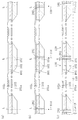
次に、半導体ウェーハ101を切断線Lに沿ってダイシングして各チップを分離し、チップ100aを形成する。このためには、半導体ウェーハ101の裏面にダイシングテープ116を貼り付け、ブレードを用いてダイシングする。図2(e)には、チップ100a二つ程度の範囲について、ダイシングした状態が示されている。尚、ダイシングテープ116としては、例えばポリオレフィン製テープにアクリル系接着剤を塗布したものを用いても良い。
Next, the
このようなダイシングは、切断クズの除去を目的として例えば洗浄用の水を供給しながら行なう。固定膜104は薄い膜であるが、犠牲層113上に積層されているため、供給される水の圧力を受けても容易に破壊されることはない。
Such dicing is performed while supplying cleaning water, for example, for the purpose of removing cutting waste. Although the fixed
この後、ダイシングテープ116を剥離してチップ100aの状態でエッチング処理を行ない、犠牲層113を除去することにより空隙102aとする。これにより、図1に示すMEMSマイクチップ100の構造を得ることができる。尚、このエッチングの際、エッチング液としてはHFを用いることができる。
Thereafter, the dicing
以上のように、チップ化のためのダイシングを犠牲層113の除去の前に行なうことにより、固定膜104の破壊を抑えることができる。その後、ダイシングの後に犠牲層113を除去すると、振動膜103と固定膜104とが空隙102aを挟んで形成された構造を有する半導体装置(MEMSマイクチップ100)を歩留り良く製造することができる。
As described above, by performing dicing for chip formation before the removal of the
また、ダイシング工程において生じる切断クズが図14に示したようなコンタミネーション201として空隙102a内に残ることは防がれている。
Further, it is possible to prevent cutting waste generated in the dicing process from remaining in the
つまり、ダイシングの際、半導体ウェーハ101、中間膜102、ダイシングテープ116等のクズが生じ、また、ダイシングブレードの破片がクズとして生じることもある。このようなクズは、孔103b又は音孔104aよりも小さい場合もあり、仮に犠牲層113が無かったとすると空隙102a内に入り込むことも考えられる。このようにして、図14のようにMEMSマイクチップ100の完成品においてコンタミネーション201が発生すると、装置の品質を劣化させる。
That is, during dicing, the
しかし、本実施形態の方法によると、ダイシングの際には犠牲層113が残されている。よって、図14に示すコンタミネーション201の発生は防がれている。結果として、MEMSマイクチップ100の品質及びその製造歩留りが向上する。
However, according to the method of the present embodiment, the
尚、以上に説明した工程においては、固定膜104の形成の後で且つ貫通孔101aの形成の前に、半導体ウェーハ101のバックグラインドを行なっている。しかし、バックグラインドは、図2(a)に示す振動膜103形成の前に行なっておくことも可能である。この場合は、既に厚さの薄くなった半導体ウェーハ101を用いて図2(a)と同様に振動膜103の形成を行なうことになる。
In the process described above, the back grinding of the
更に、固定膜104の形成の後、先に貫通孔101aの形成を行ない、その後にバックグラインドを行なってもよい。
Furthermore, after forming the fixed
このように、図2(a)〜(e)に示したものとは異なる工程順によりMEMSマイクチップ100を製造することもできる。
As described above, the
(第1の実施形態の変形例)
次に、第1の実施形態の変形例に係る半導体装置の製造方法を説明する。本変形例では、第1の実施形態の半導体装置の製造方法と比較すると、固定膜104上に保護膜を設けることを特徴とする。これについて、図面を参照して以下に説明する。図3(a)及び(b)は、本変形例における特徴的な工程を示す図である。
(Modification of the first embodiment)
Next, a method for manufacturing a semiconductor device according to a modification of the first embodiment will be described. The present modification is characterized in that a protective film is provided on the fixed
まず、第1の実施形態と同様に、図2(a)〜(d)に説明した工程を行なう。次に、図3(a)に示すように、固定膜104上に保護膜117を形成する。また、半導体ウェーハ101の裏面にダイシングテープ116を貼り付ける。この後、保護膜117と共に半導体ウェーハ101を切断線Lに沿ってブレードダイシングすることにより、図3(b)に示すようにチップ100aを得る。このようにすると、保護膜117により固定膜104の破壊を更に確実に抑制し、MEMSマイクチップ100の製造歩留りを向上することができる。尚、保護膜117は、アクリル等を材料として形成することができる。
First, similarly to the first embodiment, the steps described in FIGS. 2A to 2D are performed. Next, as shown in FIG. 3A, a
この後、保護膜117を除去する。これは、ダイシングの後、保護膜117除去のための独立した工程として行なうことも可能である。この場合には、保護膜117の除去の後、エッチングにより犠牲層113を除去することにより図1に示す半導体装置を得ることができる。
Thereafter, the
また、独立した工程として保護膜117を除去するのに代えて、犠牲層113を除去するためのエッチングの際に、保護膜117を同時に除去するようにすることも可能である。このようにすると、工程数の増加を抑えて図1に示す半導体装置を得ることができる。
Further, instead of removing the
(第2の実施形態)
次に、本発明の第2の実施形態に係る半導体装置の製造方法について図面を参照して説明する。本実施形態でも、図1に示すMEMSマイクチップ100を例として説明する。また、犠牲層113の除去及びチップ化の工程以外については第1の実施形態と同様であるため、本実施形態におけるチップ化の工程について主に説明する。尚、図4(a)及び(b)と、図5(a)及び(b)とは、本実施形態における半導体装置の製造工程を説明する図である。
(Second Embodiment)
Next, a method for manufacturing a semiconductor device according to the second embodiment of the present invention will be described with reference to the drawings. In this embodiment, the
具体的には、まず、第1の実施形態と同様に、図2(a)〜(d)の工程を行なう。これにより、図2(d)に示したように、各チップとなる構造を複数有する半導体ウェーハ101を得ることができる。
Specifically, first, similarly to the first embodiment, the steps of FIGS. 2A to 2D are performed. As a result, as shown in FIG. 2D, a
次に、図4(a)に示すように、半導体ウェーハ101に対してエッチング処理を行なうことにより、ウェーハ状態のまま犠牲層113を除去して空隙102aとする。尚、図4(a)においても、後にダイシングされる位置である切断線Lを示しており、切断線Lに挟まれた範囲が後にダイシングにより一つのチップとなる。このため、図4(a)には、半導体ウェーハ101のうち、チップ二つ程度の範囲を示していることになる。
Next, as shown in FIG. 4A, by performing an etching process on the
次に、図4(b)に示すように、半導体ウェーハ101の裏面側から切断線Lに沿ってダイシング用のレーザ118を照射する。これにより、レーザ118を照射された部分(切断線Lの近傍)の半導体ウェーハ101、中間膜102及び固定膜104は変質し、物理的強度の低下した変質層202となる。
Next, as shown in FIG. 4B, a dicing
このため、続いて図4(c)に示すように半導体ウェーハ101の裏面にダイシング用テープを貼り付け、エキスパンドを行なうと、半導体ウェーハ101等がレーザ118を照射された位置において切断され、チップ化される。ここで、エキスパンドとは、レーザ118照射後の半導体ウェーハ101に対して面に沿った方向の力を加えるため、ダイシングテープ116を広げるように引くことである。図4(c)では、矢印Fのようにダイシングテープ116を引くことを示している。
Therefore, as shown in FIG. 4 (c), when a dicing tape is applied to the back surface of the
以上のようにして、図1に示すようなMEMSマイクチップ100を製造することができる。
As described above, the
尚、分割された個々のチップについて、周囲に変質層202が残されている。照射したレーザの出力が1〜10Wである場合、残されている変質層202の幅Kは、1〜5μm程度となる。
Note that the altered
図4(b)及び(c)において、レーザが照射された切断腺Lの部分の半導体ウェーハ101、中間膜102及び固定膜104が全て変質層202となっているように示されている。しかし、より限られた範囲だけが変質層202となり、変質されることなく残っている部分があっても良い。図4(c)のエキスパンドによりチップ100が分離される程度に変質層202が形成されていればよい。
4B and 4C, it is shown that the
また、変質層202とは、代表的には多結晶質層である。つまり、本実施形態の半導体ウェーハ101として単結晶のシリコンからなるウェーハを用いることができ、この場合、レーザ照射を行なった部分の結晶構造が変化して多結晶質層である変質層202となる。
The altered
単結晶のシリコンにおいては、理想的には、全ての原子が規則正しく配列してダイヤモンド格子構造を取っている。これに対して多結晶質層の場合、部分的には原子配列が規則的に配列した結晶構造が見られるが、このような部分的な結晶構造が多数集まった構造となっており、広い領域に亘る規則正しい配列は有していない。このように、レーザ照射により、原子配列が規則的な配列を有する領域が小さくなる。 In single crystal silicon, ideally, all atoms are regularly arranged to form a diamond lattice structure. In contrast, in the case of a polycrystalline layer, a crystal structure in which atomic arrangements are regularly arranged is partially observed. However, a large number of such partial crystal structures are gathered. Does not have a regular array of Thus, the region where the atomic arrangement has a regular arrangement is reduced by laser irradiation.
このような単結晶及び多結晶の違いは、例えば、ラマン分光法等を用いて確認することができる。 Such a difference between single crystal and polycrystal can be confirmed using, for example, Raman spectroscopy.
このようなレーザ照射及びエキスパンドによるレーザダイシングは、洗浄水を供給することなく行なわれる。このため、空隙102a上に位置している固定膜104が、洗浄水の圧力等によって破壊されることはない。
Laser dicing by such laser irradiation and expansion is performed without supplying cleaning water. For this reason, the fixed
このように、ダイシング前にウェーハ状態で犠牲層113を除去する場合であっても、ダイシングをレーザダイシングとすることにより、洗浄水の圧力によって固定膜104が破壊されることを避けてダイシングを行なうことができる。このため、MEMSマイクチップ100を製造する際の歩留りを向上することができる。
Thus, even when the
尚、レーザ照射の前に、図5(a)のように、固定膜104上に表面保護テープ119を貼り付けても良い。この後、半導体ウェーハ101の裏面からレーザ118を照射する。更に、半導体ウェーハ101の裏面にダイシングテープ116を貼り付け、表面保護テープ119を剥離すると、図4(c)と同様にエキスパンドを行なうことができる。このように表面保護テープ119を用いると、ダイシングの際に固定膜104等が損傷を受けることを防ぎ、更に確実にMEMSマイクチップ100を製造することができる。更に、表面保護テープ119により、空隙102a内へのコンタミネーション201の侵入(図14を参照)を防ぐことができる。
Before the laser irradiation, a surface
また、半導体ウェーハ101に対するエッチング処理により犠牲層113を除去した後、図5(b)に示すように、半導体ウェーハ101の裏面にダイシングテープ116を貼り付けるようにしても良い。この場合、半導体ウェーハ101の表面側からレーザ118を照射する。この後、やはり図4(c)に示すようなエキスパンドを行ない、半導体ウェーハ101をレーザ照射による変質部分において切断し、チップ化することが可能である。
Alternatively, after removing the
このように、レーザ照射については、半導体ウェーハ101の表面側及び裏面側のどちらから行なっても良い。図5(a)及び(b)の場合にもレーザ照射により変質層が生じるが、その図示は省略する。
As described above, the laser irradiation may be performed from either the front surface side or the back surface side of the
レーザ118を照射する切断線Lにおいて、レーザを入射する面に酸化膜又は金属膜等が存在すると、レーザ118が反射されることがある。このようにレーザの反射が起こる場合、レーザダイシングは困難である。しかし、前記の通り、レーザ照射は半導体ウェーハ101のどちらの面から行なうことも可能である。そのため表面及び裏面のどちらか一方について、酸化膜又は金属膜等の無い面になっていれば、レーザダイシングによるチップ化が可能である。
If an oxide film or a metal film is present on the laser incident surface in the cutting line L to which the
尚、本実施形態におけるそれぞれの構成要素について、いずれも第1の実施形態と同様の材料を用いることができる。エッチングに使用する薬液等についても、第1の実施形態と同様である。 For each component in the present embodiment, the same material as in the first embodiment can be used. The chemical solution used for etching is the same as in the first embodiment.
(第2の実施形態の変形例)
以下に、第2の実施形態の変形例を説明する。図6(a)〜(c)は、本変形例に係る半導体装置の製造工程を説明する図である。本変形例では、始めに、第1の実施形態と同様に固定膜104の形成までを行ない、図2(b)に示す構造を得る。
(Modification of the second embodiment)
Below, the modification of 2nd Embodiment is demonstrated. 6A to 6C are diagrams for explaining a manufacturing process of the semiconductor device according to the present modification. In this modification, first, the formation of the fixed
次に、半導体ウェーハ101の裏面にマスク115を形成し、半導体ウェーハ101に対して裏面からエッチングを行なう。これにより、貫通孔101bが形成され、振動膜103の裏面が貫通孔101bの側に露出する。この様子を図6(a)に示す。
Next, a
次に、図6(b)に示すように、エッチングにより犠牲層113を除去して空隙102aとする。続いて、図6(c)に示すように表面保護テープ119を固定膜104上に貼り付けた後、半導体ウェーハ101の裏面を研磨する(バックグラインドを行なう)。これにより、半導体ウェーハ101の厚さが薄くなる。つまり、本変形例を第2の実施形態と比較すると、犠牲層113を除去する工程と、バックグラインドを行なう工程とについて、順序が逆になっている。
Next, as shown in FIG. 6B, the
続いて、図5(a)に示すのと同様のレーザ照射を行なう。これにより、レーザ118を照射された部分が変質して物理的に脆弱になる。更に、図4(c)と同様にダイシングテープ116を貼り付けると共に表面保護テープ119を剥離した後、エキスパンドを行なう。これにより、レーザ118を照射部分において半導体ウェーハ101、中間膜102及び固定膜104が切断され、振動膜103上に空隙102aを挟んで固定膜104が形成された構造を含む個々のチップを得ることができる。
Subsequently, laser irradiation similar to that shown in FIG. As a result, the portion irradiated with the
本変形例によると、表面保護テープ119を用いてバックグラインド及びレーザ照射の二つの工程を行なうことができる。つまり、第2の実施形態の場合のようにバックグラインドに用いたBGテープ114を剥がした後、表面保護テープ119を用いてレーザ照射を行なう場合に比べ、使用するテープの数を減らすことができる。また、テープの貼り付け及び剥離の工程についても減らすことができる。この結果、製造工程の簡略化及びコスト低減が可能である。
According to this modification, two processes of back grinding and laser irradiation can be performed using the
(第3の実施形態)
次に、本発明の第3の実施形態に係る半導体装置の製造方法について図面を参照して説明する。本実施形態でも、図1に示すMEMSマイクチップ100を例として説明する。また、犠牲層113の除去及びチップ化の工程以外については第1の実施形態と同様であるため、主として本実施形態におけるチップ化の工程について説明する。尚、図7(a)〜(c)と、図8(a)及び(b)とは、本実施形態に係る半導体装置の製造方法を説明する図である。
(Third embodiment)
Next, a method for manufacturing a semiconductor device according to the third embodiment of the present invention will be described with reference to the drawings. In this embodiment, the
具体的には、まず、第1の実施形態と同様に、図2(a)〜(d)の工程を行なう。これにより、図2(d)に示したように、振動膜103上に犠牲層113を介して固定膜104が形成された構造を複数有する半導体ウェーハ101を得ることができる。
Specifically, first, similarly to the first embodiment, the steps of FIGS. 2A to 2D are performed. Thereby, as shown in FIG. 2D, the
次に、図7(a)に示すように、半導体ウェーハ101に対してエッチング処理を行なうことにより、ウェーハ状態のまま犠牲層113を除去して空隙102aとする。尚、図7(a)においても、後にダイシングされる位置である切断線Lを示している。ここでも、ダイシングによりチップとなる範囲が二つ程度示されている。
Next, as shown in FIG. 7A, the
次に、図7(b)に示すように、固定膜104上に、保護膜117を形成する。これは、例えば、アクリル等を材料として形成すればよい。更に、半導体ウェーハ101の裏面に、ダイシングテープ116を貼り付ける。
Next, as shown in FIG. 7B, a
続いて、図7(c)に示すように、保護膜117と共に半導体ウェーハ101をブレードダイシングする。このとき、固定膜104上に保護膜117が形成されていることにより、ダイシングに伴う洗浄水の圧力によって固定膜104が破壊されることは抑えられている。
Subsequently, as shown in FIG. 7C, the
このようにして、洗浄水の供給を伴うブレードダイシングを用いる場合であっても、保護膜117により固定膜104が破壊されることを抑制しながらダイシングを行ない、チップを得ることができる。
In this way, even when blade dicing with cleaning water supply is used, dicing is performed while suppressing destruction of the fixed
このようなダイシングの際、保護膜117が形成されていることにより、図14に示すような空隙102a内におけるコンタミネーション201の発生は防がれている。
In such dicing, the formation of the
この後、保護膜117を除去すると、図1と同様のMEMSマイクチップ100を得ることができる。保護膜117の除去のためには、例えば、図8(a)のようにダイシングされたチップをダイシングテープ116から外してチップホルダー120に移し、その後IPA(イソプロピルアルコール)等による洗浄等を行なえばよい。このようにすると、より確実な洗浄を行なうことができる。
Thereafter, when the
また、保護膜117を除去するための別の方法としては、図8(b)のように、ダイシングテープ116に貼り付けられた状態のままのチップに対してIPA洗浄を行なうこともできる。この場合、チップをチップホルダーに移す作業が不要であるため、より簡便な工程となる利点がある。
As another method for removing the
以上のようにして、振動膜103上に空隙102aを介して固定膜104が形成された構造を有する半導体装置、具体的にはMEMSマイクチップ100を歩留り良く製造することができる。更に、コンタミネーションの発生が防止されていることによる品質及び歩留りの向上も実現する。
As described above, a semiconductor device having a structure in which the fixed
尚、以上に説明した工程では、固定膜104を形成した後にバックグラインド、その次に貫通孔101aの形成という順序となっている。しかし、第1の実施形態の場合と同様、バックグラインドは、振動膜103を形成する前に行なっても良い。
In the steps described above, the order is the back grind after the fixing
また、バックグラインドは、保護膜117の形成後で且つダイシングの前に行なうこともできる。図9(a)〜(c)は、このような場合の工程を説明する図である。
Further, the back grinding can be performed after the formation of the
つまり、図2(b)の構造を形成した後、図9(a)に示すように、半導体ウェーハ101の裏面にマスク115を設けた後、これをマスクとするエッチングにより貫通孔101bを形成する。
That is, after the structure of FIG. 2B is formed, as shown in FIG. 9A, a
次に、図9(b)に示すように、固定膜104上に保護膜117を形成する。続いて、保護膜117上にBGテープ114を貼り付け、半導体ウェーハ101のバックグラインドを行なう。これにより、図9(c)に示すように、半導体ウェーハ101の厚さを裏面から薄くする。続いて、BGテープ114を剥がした後、図7(b)及び(c)と同様に、ダイシングテープ116を貼り付けてブレードダイシングを行なう。保護膜117の除去についても、先に説明した場合と同様である。
Next, as shown in FIG. 9B, a
(第4の実施形態)
次に、本発明の第4の実施形態に係る半導体装置の製造方法について、図面を参照して説明する。図10(a)及び(b)と、図11(a)〜(c)とは、本実施形態における半導体装置の製造方法を説明する図である。
(Fourth embodiment)
Next, a method for manufacturing a semiconductor device according to the fourth embodiment of the present invention will be described with reference to the drawings. FIGS. 10A and 10B and FIGS. 11A to 11C are views for explaining a method of manufacturing a semiconductor device according to this embodiment.
本実施形態でも、図1に示すMEMSマイクチップ100を例として説明する。また、犠牲層113の除去及びチップ化の工程以外については第1の実施形態と同様であるため、本実施形態におけるチップ化の工程について主に説明する。
In this embodiment, the
まず、第1の実施形態と同様にして固定膜104の形成までを行ない、図2(b)に示す構造を得る。つまり、半導体ウェーハ101上に振動膜103が形成され、その上に犠牲層113を介して固定膜104が形成された構造である。この時点では、バックグラインドは行なわれていない。
First, similarly to the first embodiment, the formation up to the fixed
次に、図10(a)に示すように、半導体ウェーハ101の裏面(振動膜103が形成されているのと反対側の面)にマスク115を形成し、半導体ウェーハ101に対して裏面からエッチングを行なう。これにより、貫通孔101bが形成され、振動膜103の裏面が貫通孔101bの側に露出する。
Next, as shown in FIG. 10A, a
次に、半導体ウェーハ101の表面からブレードダイシングを行なう。但し、図10(b)に示すように、半導体ウェーハ101の裏面付近において、半導体ウェーハ101の一部を薄い接続部121として残し、表面から溝122を設けるようにブレードダイシングを行なう。この結果、半導体ウェーハ101における各チップとなるべき領域が、半導体ウェーハ101を薄く残した部分である接続部121によって繋がった状態となる。
Next, blade dicing is performed from the surface of the
このようなブレードダイシングの際、固定膜104は犠牲層113上に積層されているため、洗浄水の圧力によって破壊されることは避けられている。また、犠牲層113が存在するため、ダイシングの際に発生するクズにより図14に示すようなコンタミネーション201が残ることは防がれている。
During such blade dicing, since the fixed
次に、図11(a)に示すように、溝122の形成された半導体ウェーハ101に対するエッチング処理により、犠牲層113を除去して空隙102aとする。
Next, as shown in FIG. 11A, the
続いて、図11(b)に示すように、固定膜104上にBGテープ114を貼り付けた後、半導体ウェーハ101の裏面を研磨する。このようなバックグラインドは、少なくとも、接続部121を削り取って溝122に達するまで行なう。これにより、接続部121によって互いに接続されていた個々のチップとなる領域が切り離され、図1に示すのと同じMEMSマイクチップ100を形成することができる。
Subsequently, as shown in FIG. 11B, after the
この後、図11(c)に示すように、個々のチップの裏面に接するようにダイシングテープ116を貼り付ける。更に、BGテープ114を剥離すると、ダイシングテープ116に対する転写を行なうことができる。
Thereafter, as shown in FIG. 11C, a dicing
以上のように、それぞれ振動膜103及び固定膜104を含むチップとなる領域を囲むように、ダイシングによって溝122を半導体ウェーハ101の表面から形成した後、犠牲層113を除去し、更にその後、半導体ウェーハ101の裏面からバックグラインドを行なう。このような方法によると、固定膜104が破壊されるのを抑制しながら、MEMSマイクチップ100のような半導体装置を製造することができる。また、ダイシング工程におけるコンタミネーションの発生を防ぐことにより、品質と製造歩留りの向上とを実現している。
As described above, the
尚、犠牲層113を除去するためのエッチングを行なう際、溝122の側面についてもエッチングされ、溝122の幅が広くなることがある。例えば、図12に示すように、切断線Lから側面侵食位置Eまでエッチングされることがある。このようなことが起こると、製造される半導体装置(MEMSマイクチップ100)の機能に影響するおそれがある。
Note that when etching for removing the
そこで、例えば図12に示すように、切断線Lから後に空隙102aとなる犠牲層113までの距離Mについて、エッチング処理により溝122の側面の側面がエッチングされる量を予め考慮してマージンを含めた距離としておく。これにより、例えば側面侵食位置Eまで溝122の側面がエッチングされた場合にも、製造される半導体装置の機能に影響が及ぶのを避けることができる。
Therefore, for example, as shown in FIG. 12, with respect to the distance M from the cutting line L to the
尚、以上のいずれの実施形態においても、記載した各構成要素の材料等はいずれも例示するものであり、特に限定されない。 In any of the above-described embodiments, the materials and the like of the constituent elements described are merely examples and are not particularly limited.
本発明に係る半導体装置の製造方法によると、脆弱な構造である部分がダイシングの際に破壊されるのを避けると共に、コンタミネーションを避けて半導体ウェーハのチップ化を行なうことができ、特に、MEMSマイクチップ等の製造に有用である。 According to the method for manufacturing a semiconductor device according to the present invention, a portion having a fragile structure can be prevented from being destroyed during dicing, and a semiconductor wafer can be formed into chips by avoiding contamination. This is useful for manufacturing microphone chips and the like.
100 MEMSマイクチップ
100a チップ
101 半導体ウェーハ
102 中間膜
102a 空隙
102b 貫通孔
103 振動膜
103a 積層材料膜
104 固定膜
104b 孔
111 エッチングストッパー膜
112 酸化膜
113 犠牲層
114 BGテープ
115 マスク
116 ダイシングテープ
117 保護膜
118 レーザ
119 表面保護テープ
120 チップホルダー
121 接続部
122 溝
201 コンタミネーション
202 変質層
100
Claims (15)
前記各チップの前記振動膜上に位置する犠牲層を含む中間膜を前記半導体ウェーハ上に形成する工程(b)と、
前記中間膜上に固定膜を形成する工程(c)と、
前記各チップに貫通孔を形成する工程(d)と、
前記犠牲層を除去して前記振動膜と前記固定膜との間に空隙を設ける工程(e)と、
前記半導体ウェーハの前記固定膜が形成された面とは反対の面にダイシングテープを貼り付けた後、酸化膜又は金属膜が形成されていないスクライブレーンの切断線に沿って、前記固定膜が形成された面側から、前記固定膜が露出した状態で、前記各チップの周囲にレーザ照射を行なうことにより、前記各チップを囲む変質層を形成し、前記半導体ウェーハに外力を加えることにより前記変質層に沿って前記各チップを分離する工程(f)とを備え、
前記犠牲膜を除去して空隙を設ける工程(e)の後に、前記チップを分離する工程(f)が行なわれることを特徴とするMEMSマイクの製造方法。 A step (a) of forming a vibration film on a predetermined region of each chip in a semiconductor wafer having a plurality of chips;
Forming an intermediate film including a sacrificial layer located on the vibration film of each chip on the semiconductor wafer (b);
Forming a fixed film on the intermediate film (c);
Forming a through hole in each of the chips (d);
Removing the sacrificial layer and providing a gap between the vibrating membrane and the fixed membrane;
After fixing a dicing tape on the surface of the semiconductor wafer opposite to the surface on which the fixed film is formed, the fixed film is formed along a cutting line of a scribe lane in which no oxide film or metal film is formed. In the state where the fixed film is exposed from the formed surface side, laser irradiation is performed around each of the chips to form an altered layer surrounding each of the chips, and the altered wafer is applied by applying an external force to the semiconductor wafer. Separating each chip along the layer (f),
A method of manufacturing a MEMS microphone, wherein the step (f) of separating the chip is performed after the step (e) of removing the sacrificial film and providing a gap.
Priority Applications (6)
| Application Number | Priority Date | Filing Date | Title |
|---|---|---|---|
| JP2007001227A JP4480728B2 (en) | 2006-06-09 | 2007-01-09 | Method for manufacturing MEMS microphone |
| US11/798,676 US20070287215A1 (en) | 2006-06-09 | 2007-05-16 | Method for fabricating semiconductor device |
| CN2011100600350A CN102161471A (en) | 2006-06-09 | 2007-05-29 | Method for fabricating semiconductor device |
| CN2007101064301A CN101086956B (en) | 2006-06-09 | 2007-05-29 | Method for fabricating semiconductor device |
| US12/578,040 US7838323B2 (en) | 2006-06-09 | 2009-10-13 | Method for fabricating semiconductor device |
| US12/913,340 US20110039365A1 (en) | 2006-06-09 | 2010-10-27 | Method for fabricating semiconductor device |
Applications Claiming Priority (2)
| Application Number | Priority Date | Filing Date | Title |
|---|---|---|---|
| JP2006160927 | 2006-06-09 | ||
| JP2007001227A JP4480728B2 (en) | 2006-06-09 | 2007-01-09 | Method for manufacturing MEMS microphone |
Related Child Applications (1)
| Application Number | Title | Priority Date | Filing Date |
|---|---|---|---|
| JP2009162884A Division JP2009226582A (en) | 2006-06-09 | 2009-07-09 | Method for fabricating semiconductor device |
Publications (3)
| Publication Number | Publication Date |
|---|---|
| JP2008012654A JP2008012654A (en) | 2008-01-24 |
| JP2008012654A5 JP2008012654A5 (en) | 2009-07-02 |
| JP4480728B2 true JP4480728B2 (en) | 2010-06-16 |
Family
ID=38822452
Family Applications (1)
| Application Number | Title | Priority Date | Filing Date |
|---|---|---|---|
| JP2007001227A Active JP4480728B2 (en) | 2006-06-09 | 2007-01-09 | Method for manufacturing MEMS microphone |
Country Status (3)
| Country | Link |
|---|---|
| US (3) | US20070287215A1 (en) |
| JP (1) | JP4480728B2 (en) |
| CN (1) | CN102161471A (en) |
Cited By (1)
| Publication number | Priority date | Publication date | Assignee | Title |
|---|---|---|---|---|
| TWI498272B (en) * | 2012-10-09 | 2015-09-01 | Univ Feng Chia | Microelectromechanical system device and manufacturing method thereof |
Families Citing this family (105)
| Publication number | Priority date | Publication date | Assignee | Title |
|---|---|---|---|---|
| US8103027B2 (en) * | 2007-06-06 | 2012-01-24 | Analog Devices, Inc. | Microphone with reduced parasitic capacitance |
| JP2009113165A (en) * | 2007-11-07 | 2009-05-28 | Tokyo Electron Ltd | Method of manufacturing microstructure device |
| KR100921390B1 (en) | 2008-03-03 | 2009-10-14 | 씨 선 엠에프지 리미티드 | Wafer membrane cutter |
| US7863063B2 (en) * | 2008-03-04 | 2011-01-04 | Memsmart Semiconductor Corp. | Method for fabricating a sealed cavity microstructure |
| JP5207800B2 (en) * | 2008-03-31 | 2013-06-12 | 三菱電機株式会社 | Deposition method |
| JP5127669B2 (en) * | 2008-10-31 | 2013-01-23 | パナソニック株式会社 | Semiconductor wafer |
| JP2010162629A (en) * | 2009-01-14 | 2010-07-29 | Seiko Epson Corp | Method of manufacturing mems device |
| US8012785B2 (en) * | 2009-04-24 | 2011-09-06 | Taiwan Semiconductor Manufacturing Company, Ltd. | Method of fabricating an integrated CMOS-MEMS device |
| US8642448B2 (en) | 2010-06-22 | 2014-02-04 | Applied Materials, Inc. | Wafer dicing using femtosecond-based laser and plasma etch |
| US8507358B2 (en) * | 2010-08-27 | 2013-08-13 | Taiwan Semiconductor Manufacturing Company, Ltd. | Composite wafer semiconductor |
| US9029242B2 (en) | 2011-06-15 | 2015-05-12 | Applied Materials, Inc. | Damage isolation by shaped beam delivery in laser scribing process |
| US8759197B2 (en) | 2011-06-15 | 2014-06-24 | Applied Materials, Inc. | Multi-step and asymmetrically shaped laser beam scribing |
| US8507363B2 (en) | 2011-06-15 | 2013-08-13 | Applied Materials, Inc. | Laser and plasma etch wafer dicing using water-soluble die attach film |
| US9129904B2 (en) | 2011-06-15 | 2015-09-08 | Applied Materials, Inc. | Wafer dicing using pulse train laser with multiple-pulse bursts and plasma etch |
| US8703581B2 (en) | 2011-06-15 | 2014-04-22 | Applied Materials, Inc. | Water soluble mask for substrate dicing by laser and plasma etch |
| US8598016B2 (en) | 2011-06-15 | 2013-12-03 | Applied Materials, Inc. | In-situ deposited mask layer for device singulation by laser scribing and plasma etch |
| US8557683B2 (en) | 2011-06-15 | 2013-10-15 | Applied Materials, Inc. | Multi-step and asymmetrically shaped laser beam scribing |
| US9126285B2 (en) | 2011-06-15 | 2015-09-08 | Applied Materials, Inc. | Laser and plasma etch wafer dicing using physically-removable mask |
| US8557682B2 (en) | 2011-06-15 | 2013-10-15 | Applied Materials, Inc. | Multi-layer mask for substrate dicing by laser and plasma etch |
| US8912077B2 (en) | 2011-06-15 | 2014-12-16 | Applied Materials, Inc. | Hybrid laser and plasma etch wafer dicing using substrate carrier |
| US8951819B2 (en) | 2011-07-11 | 2015-02-10 | Applied Materials, Inc. | Wafer dicing using hybrid split-beam laser scribing process with plasma etch |
| TWI488231B (en) * | 2012-01-18 | 2015-06-11 | Xintec Inc | Semiconductor package and manufacturing method thereof and system for manufacturing the same |
| JP5914010B2 (en) | 2012-01-30 | 2016-05-11 | ルネサスエレクトロニクス株式会社 | Manufacturing method of semiconductor integrated circuit device |
| US8652940B2 (en) | 2012-04-10 | 2014-02-18 | Applied Materials, Inc. | Wafer dicing used hybrid multi-step laser scribing process with plasma etch |
| DE102012205921A1 (en) * | 2012-04-12 | 2013-10-17 | Robert Bosch Gmbh | Membrane assembly for a micro-electro-mechanical transmitter and method of making a diaphragm assembly |
| US8946057B2 (en) | 2012-04-24 | 2015-02-03 | Applied Materials, Inc. | Laser and plasma etch wafer dicing using UV-curable adhesive film |
| US8969177B2 (en) | 2012-06-29 | 2015-03-03 | Applied Materials, Inc. | Laser and plasma etch wafer dicing with a double sided UV-curable adhesive film |
| US9048309B2 (en) | 2012-07-10 | 2015-06-02 | Applied Materials, Inc. | Uniform masking for wafer dicing using laser and plasma etch |
| US8993414B2 (en) | 2012-07-13 | 2015-03-31 | Applied Materials, Inc. | Laser scribing and plasma etch for high die break strength and clean sidewall |
| US8859397B2 (en) | 2012-07-13 | 2014-10-14 | Applied Materials, Inc. | Method of coating water soluble mask for laser scribing and plasma etch |
| US8940619B2 (en) | 2012-07-13 | 2015-01-27 | Applied Materials, Inc. | Method of diced wafer transportation |
| US8845854B2 (en) | 2012-07-13 | 2014-09-30 | Applied Materials, Inc. | Laser, plasma etch, and backside grind process for wafer dicing |
| US9159574B2 (en) | 2012-08-27 | 2015-10-13 | Applied Materials, Inc. | Method of silicon etch for trench sidewall smoothing |
| US9252057B2 (en) | 2012-10-17 | 2016-02-02 | Applied Materials, Inc. | Laser and plasma etch wafer dicing with partial pre-curing of UV release dicing tape for film frame wafer application |
| JP2014086447A (en) | 2012-10-19 | 2014-05-12 | Seiko Epson Corp | Electronic apparatus and manufacturing method of the same |
| US8975162B2 (en) | 2012-12-20 | 2015-03-10 | Applied Materials, Inc. | Wafer dicing from wafer backside |
| US9236305B2 (en) | 2013-01-25 | 2016-01-12 | Applied Materials, Inc. | Wafer dicing with etch chamber shield ring for film frame wafer applications |
| US8980726B2 (en) | 2013-01-25 | 2015-03-17 | Applied Materials, Inc. | Substrate dicing by laser ablation and plasma etch damage removal for ultra-thin wafers |
| WO2014159464A1 (en) | 2013-03-14 | 2014-10-02 | Applied Materials, Inc. | Multi-layer mask including non-photodefinable laser energy absorbing layer for substrate dicing by laser and plasma etch |
| US8883614B1 (en) | 2013-05-22 | 2014-11-11 | Applied Materials, Inc. | Wafer dicing with wide kerf by laser scribing and plasma etching hybrid approach |
| US9105710B2 (en) | 2013-08-30 | 2015-08-11 | Applied Materials, Inc. | Wafer dicing method for improving die packaging quality |
| US9224650B2 (en) | 2013-09-19 | 2015-12-29 | Applied Materials, Inc. | Wafer dicing from wafer backside and front side |
| US9460966B2 (en) | 2013-10-10 | 2016-10-04 | Applied Materials, Inc. | Method and apparatus for dicing wafers having thick passivation polymer layer |
| US9041198B2 (en) | 2013-10-22 | 2015-05-26 | Applied Materials, Inc. | Maskless hybrid laser scribing and plasma etching wafer dicing process |
| US9312177B2 (en) | 2013-12-06 | 2016-04-12 | Applied Materials, Inc. | Screen print mask for laser scribe and plasma etch wafer dicing process |
| US9299614B2 (en) | 2013-12-10 | 2016-03-29 | Applied Materials, Inc. | Method and carrier for dicing a wafer |
| US9293304B2 (en) | 2013-12-17 | 2016-03-22 | Applied Materials, Inc. | Plasma thermal shield for heat dissipation in plasma chamber |
| US9018079B1 (en) | 2014-01-29 | 2015-04-28 | Applied Materials, Inc. | Wafer dicing using hybrid laser scribing and plasma etch approach with intermediate reactive post mask-opening clean |
| US9012305B1 (en) | 2014-01-29 | 2015-04-21 | Applied Materials, Inc. | Wafer dicing using hybrid laser scribing and plasma etch approach with intermediate non-reactive post mask-opening clean |
| US9299611B2 (en) | 2014-01-29 | 2016-03-29 | Applied Materials, Inc. | Method of wafer dicing using hybrid laser scribing and plasma etch approach with mask plasma treatment for improved mask etch resistance |
| US8927393B1 (en) | 2014-01-29 | 2015-01-06 | Applied Materials, Inc. | Water soluble mask formation by dry film vacuum lamination for laser and plasma dicing |
| US9236284B2 (en) | 2014-01-31 | 2016-01-12 | Applied Materials, Inc. | Cooled tape frame lift and low contact shadow ring for plasma heat isolation |
| US8991329B1 (en) | 2014-01-31 | 2015-03-31 | Applied Materials, Inc. | Wafer coating |
| US20150255349A1 (en) | 2014-03-07 | 2015-09-10 | JAMES Matthew HOLDEN | Approaches for cleaning a wafer during hybrid laser scribing and plasma etching wafer dicing processes |
| US9130030B1 (en) | 2014-03-07 | 2015-09-08 | Applied Materials, Inc. | Baking tool for improved wafer coating process |
| US9275902B2 (en) | 2014-03-26 | 2016-03-01 | Applied Materials, Inc. | Dicing processes for thin wafers with bumps on wafer backside |
| US9076860B1 (en) | 2014-04-04 | 2015-07-07 | Applied Materials, Inc. | Residue removal from singulated die sidewall |
| US8975163B1 (en) | 2014-04-10 | 2015-03-10 | Applied Materials, Inc. | Laser-dominated laser scribing and plasma etch hybrid wafer dicing |
| US8932939B1 (en) | 2014-04-14 | 2015-01-13 | Applied Materials, Inc. | Water soluble mask formation by dry film lamination |
| US8912078B1 (en) | 2014-04-16 | 2014-12-16 | Applied Materials, Inc. | Dicing wafers having solder bumps on wafer backside |
| US8999816B1 (en) | 2014-04-18 | 2015-04-07 | Applied Materials, Inc. | Pre-patterned dry laminate mask for wafer dicing processes |
| US9159621B1 (en) | 2014-04-29 | 2015-10-13 | Applied Materials, Inc. | Dicing tape protection for wafer dicing using laser scribe process |
| US8912075B1 (en) | 2014-04-29 | 2014-12-16 | Applied Materials, Inc. | Wafer edge warp supression for thin wafer supported by tape frame |
| US8980727B1 (en) | 2014-05-07 | 2015-03-17 | Applied Materials, Inc. | Substrate patterning using hybrid laser scribing and plasma etching processing schemes |
| US9112050B1 (en) | 2014-05-13 | 2015-08-18 | Applied Materials, Inc. | Dicing tape thermal management by wafer frame support ring cooling during plasma dicing |
| US9034771B1 (en) | 2014-05-23 | 2015-05-19 | Applied Materials, Inc. | Cooling pedestal for dicing tape thermal management during plasma dicing |
| US9142459B1 (en) | 2014-06-30 | 2015-09-22 | Applied Materials, Inc. | Wafer dicing using hybrid laser scribing and plasma etch approach with mask application by vacuum lamination |
| US9165832B1 (en) | 2014-06-30 | 2015-10-20 | Applied Materials, Inc. | Method of die singulation using laser ablation and induction of internal defects with a laser |
| US9130057B1 (en) | 2014-06-30 | 2015-09-08 | Applied Materials, Inc. | Hybrid dicing process using a blade and laser |
| US9093518B1 (en) | 2014-06-30 | 2015-07-28 | Applied Materials, Inc. | Singulation of wafers having wafer-level underfill |
| US9349648B2 (en) | 2014-07-22 | 2016-05-24 | Applied Materials, Inc. | Hybrid wafer dicing approach using a rectangular shaped two-dimensional top hat laser beam profile or a linear shaped one-dimensional top hat laser beam profile laser scribing process and plasma etch process |
| US9196498B1 (en) | 2014-08-12 | 2015-11-24 | Applied Materials, Inc. | Stationary actively-cooled shadow ring for heat dissipation in plasma chamber |
| US9117868B1 (en) | 2014-08-12 | 2015-08-25 | Applied Materials, Inc. | Bipolar electrostatic chuck for dicing tape thermal management during plasma dicing |
| US9281244B1 (en) | 2014-09-18 | 2016-03-08 | Applied Materials, Inc. | Hybrid wafer dicing approach using an adaptive optics-controlled laser scribing process and plasma etch process |
| US9177861B1 (en) | 2014-09-19 | 2015-11-03 | Applied Materials, Inc. | Hybrid wafer dicing approach using laser scribing process based on an elliptical laser beam profile or a spatio-temporal controlled laser beam profile |
| US11195756B2 (en) | 2014-09-19 | 2021-12-07 | Applied Materials, Inc. | Proximity contact cover ring for plasma dicing |
| US9196536B1 (en) | 2014-09-25 | 2015-11-24 | Applied Materials, Inc. | Hybrid wafer dicing approach using a phase modulated laser beam profile laser scribing process and plasma etch process |
| US9130056B1 (en) | 2014-10-03 | 2015-09-08 | Applied Materials, Inc. | Bi-layer wafer-level underfill mask for wafer dicing and approaches for performing wafer dicing |
| US9245803B1 (en) | 2014-10-17 | 2016-01-26 | Applied Materials, Inc. | Hybrid wafer dicing approach using a bessel beam shaper laser scribing process and plasma etch process |
| US10692765B2 (en) | 2014-11-07 | 2020-06-23 | Applied Materials, Inc. | Transfer arm for film frame substrate handling during plasma singulation of wafers |
| KR101619253B1 (en) * | 2014-11-26 | 2016-05-10 | 현대자동차 주식회사 | Microphone and method manufacturing the same |
| KR101610129B1 (en) * | 2014-11-26 | 2016-04-20 | 현대자동차 주식회사 | Microphone and method manufacturing the same |
| US9355907B1 (en) | 2015-01-05 | 2016-05-31 | Applied Materials, Inc. | Hybrid wafer dicing approach using a line shaped laser beam profile laser scribing process and plasma etch process |
| US9330977B1 (en) | 2015-01-05 | 2016-05-03 | Applied Materials, Inc. | Hybrid wafer dicing approach using a galvo scanner and linear stage hybrid motion laser scribing process and plasma etch process |
| US9159624B1 (en) | 2015-01-05 | 2015-10-13 | Applied Materials, Inc. | Vacuum lamination of polymeric dry films for wafer dicing using hybrid laser scribing and plasma etch approach |
| US9601375B2 (en) | 2015-04-27 | 2017-03-21 | Applied Materials, Inc. | UV-cure pre-treatment of carrier film for wafer dicing using hybrid laser scribing and plasma etch approach |
| US9721839B2 (en) | 2015-06-12 | 2017-08-01 | Applied Materials, Inc. | Etch-resistant water soluble mask for hybrid wafer dicing using laser scribing and plasma etch |
| US9478455B1 (en) | 2015-06-12 | 2016-10-25 | Applied Materials, Inc. | Thermal pyrolytic graphite shadow ring assembly for heat dissipation in plasma chamber |
| JP6469854B2 (en) * | 2015-11-09 | 2019-02-13 | 古河電気工業株式会社 | Semiconductor chip manufacturing method and mask-integrated surface protection tape used therefor |
| US9972575B2 (en) | 2016-03-03 | 2018-05-15 | Applied Materials, Inc. | Hybrid wafer dicing approach using a split beam laser scribing process and plasma etch process |
| US9852997B2 (en) | 2016-03-25 | 2017-12-26 | Applied Materials, Inc. | Hybrid wafer dicing approach using a rotating beam laser scribing process and plasma etch process |
| WO2017191365A1 (en) | 2016-05-02 | 2017-11-09 | Teknologian Tutkimuskeskus Vtt Oy | Mechanically decoupled surface micromechanical element and method for manufacturing the same |
| US9793132B1 (en) | 2016-05-13 | 2017-10-17 | Applied Materials, Inc. | Etch mask for hybrid laser scribing and plasma etch wafer singulation process |
| KR102212575B1 (en) * | 2017-02-02 | 2021-02-04 | 현대자동차 주식회사 | Microphone and manufacturing method thereof |
| US11158540B2 (en) | 2017-05-26 | 2021-10-26 | Applied Materials, Inc. | Light-absorbing mask for hybrid laser scribing and plasma etch wafer singulation process |
| US10363629B2 (en) | 2017-06-01 | 2019-07-30 | Applied Materials, Inc. | Mitigation of particle contamination for wafer dicing processes |
| US10535561B2 (en) | 2018-03-12 | 2020-01-14 | Applied Materials, Inc. | Hybrid wafer dicing approach using a multiple pass laser scribing process and plasma etch process |
| US11355394B2 (en) | 2018-09-13 | 2022-06-07 | Applied Materials, Inc. | Wafer dicing using hybrid laser scribing and plasma etch approach with intermediate breakthrough treatment |
| CN109987573B (en) * | 2019-04-02 | 2021-12-14 | 无锡韦感半导体有限公司 | Semiconductor structure and manufacturing method thereof |
| KR20210006565A (en) | 2019-07-08 | 2021-01-19 | 삼성전자주식회사 | Method for plasma dicing |
| US11011424B2 (en) | 2019-08-06 | 2021-05-18 | Applied Materials, Inc. | Hybrid wafer dicing approach using a spatially multi-focused laser beam laser scribing process and plasma etch process |
| US11342226B2 (en) | 2019-08-13 | 2022-05-24 | Applied Materials, Inc. | Hybrid wafer dicing approach using an actively-focused laser beam laser scribing process and plasma etch process |
| US10903121B1 (en) | 2019-08-14 | 2021-01-26 | Applied Materials, Inc. | Hybrid wafer dicing approach using a uniform rotating beam laser scribing process and plasma etch process |
| US11600492B2 (en) | 2019-12-10 | 2023-03-07 | Applied Materials, Inc. | Electrostatic chuck with reduced current leakage for hybrid laser scribing and plasma etch wafer singulation process |
| US11211247B2 (en) | 2020-01-30 | 2021-12-28 | Applied Materials, Inc. | Water soluble organic-inorganic hybrid mask formulations and their applications |
Family Cites Families (33)
| Publication number | Priority date | Publication date | Assignee | Title |
|---|---|---|---|---|
| FR2697022B1 (en) * | 1992-10-19 | 1994-12-16 | Pasteur Institut | Plasmodium falciparum antigens capable of inducing protective antibodies with broad spectrum - Application to vaccination. |
| US5452268A (en) * | 1994-08-12 | 1995-09-19 | The Charles Stark Draper Laboratory, Inc. | Acoustic transducer with improved low frequency response |
| JP3500813B2 (en) | 1995-11-08 | 2004-02-23 | 株式会社デンソー | Semiconductor wafer cutting method |
| JP2000340527A (en) | 1999-05-28 | 2000-12-08 | Horiba Ltd | Method for separating semiconductor elements |
| US6535460B2 (en) * | 2000-08-11 | 2003-03-18 | Knowles Electronics, Llc | Miniature broadband acoustic transducer |
| JP3408805B2 (en) | 2000-09-13 | 2003-05-19 | 浜松ホトニクス株式会社 | Cutting origin region forming method and workpiece cutting method |
| JP4659300B2 (en) * | 2000-09-13 | 2011-03-30 | 浜松ホトニクス株式会社 | Laser processing method and semiconductor chip manufacturing method |
| US6759273B2 (en) * | 2000-12-05 | 2004-07-06 | Analog Devices, Inc. | Method and device for protecting micro electromechanical systems structures during dicing of a wafer |
| WO2003047307A2 (en) * | 2001-11-27 | 2003-06-05 | Corporation For National Research Initiatives | A miniature condenser microphone and fabrication method therefor |
| EP2216128B1 (en) * | 2002-03-12 | 2016-01-27 | Hamamatsu Photonics K.K. | Method of cutting object to be processed |
| US7135070B2 (en) * | 2002-04-23 | 2006-11-14 | Sharp Laboratories Of America, Inc. | Monolithic stacked/layered crystal-structure-processed mechanical, and combined mechanical and electrical, devices and methods and systems for making |
| JP2004193399A (en) * | 2002-12-12 | 2004-07-08 | Denso Corp | Semiconductor device and its manufacturing method |
| JP2004335583A (en) | 2003-05-01 | 2004-11-25 | Nippon Hoso Kyokai <Nhk> | Wafer dicing method |
| JP2005020411A (en) | 2003-06-26 | 2005-01-20 | Nippon Hoso Kyokai <Nhk> | Manufacturing method of silicon microphone |
| WO2005013349A2 (en) * | 2003-07-31 | 2005-02-10 | Fsi International, Inc. | Controlled growth of highly uniform, oxide layers, especially ultrathin layers |
| JP2005116844A (en) | 2003-10-09 | 2005-04-28 | Matsushita Electric Ind Co Ltd | Method for manufacturing semiconductor device |
| JP2005129607A (en) * | 2003-10-22 | 2005-05-19 | Disco Abrasive Syst Ltd | Method of dividing wafer |
| JP4385746B2 (en) | 2003-11-28 | 2009-12-16 | 三菱化学株式会社 | Nitride semiconductor device manufacturing method |
| JP4419563B2 (en) | 2003-12-25 | 2010-02-24 | パナソニック株式会社 | Electret condenser |
| JP2005268752A (en) | 2004-02-19 | 2005-09-29 | Canon Inc | Method of laser cutting, workpiece and semiconductor-element chip |
| JP2005244094A (en) | 2004-02-27 | 2005-09-08 | Tokyo Electron Ltd | Semiconductor device and its manufacturing method |
| JP4264103B2 (en) | 2004-03-03 | 2009-05-13 | パナソニック株式会社 | Electret condenser microphone |
| JP3875240B2 (en) * | 2004-03-31 | 2007-01-31 | 株式会社東芝 | Manufacturing method of electronic parts |
| JP4769429B2 (en) | 2004-05-26 | 2011-09-07 | ルネサスエレクトロニクス株式会社 | Manufacturing method of semiconductor device |
| JP4732063B2 (en) | 2004-08-06 | 2011-07-27 | 浜松ホトニクス株式会社 | Laser processing method |
| JP2006062002A (en) | 2004-08-25 | 2006-03-09 | Oki Electric Ind Co Ltd | Method of segmenting substrate of semiconductor device |
| JP4426413B2 (en) | 2004-09-24 | 2010-03-03 | 日本電信電話株式会社 | Manufacturing method of semiconductor device |
| JP2006114691A (en) * | 2004-10-14 | 2006-04-27 | Disco Abrasive Syst Ltd | Division method of wafer |
| JP2006196588A (en) | 2005-01-12 | 2006-07-27 | Nippon Hoso Kyokai <Nhk> | Method of manufacturing micro-machine and electrostatic capacity type sensor |
| US7373835B2 (en) * | 2005-01-31 | 2008-05-20 | Sanyo Electric Industries, Ltd. | Semiconductor sensor |
| JP2006268752A (en) | 2005-03-25 | 2006-10-05 | Seiko Epson Corp | Activation of module corresponding to a plurality of versions |
| JP4975265B2 (en) | 2005-04-05 | 2012-07-11 | 日本放送協会 | Pressure sensor and manufacturing method thereof |
| GB0605576D0 (en) * | 2006-03-20 | 2006-04-26 | Oligon Ltd | MEMS device |
-
2007
- 2007-01-09 JP JP2007001227A patent/JP4480728B2/en active Active
- 2007-05-16 US US11/798,676 patent/US20070287215A1/en not_active Abandoned
- 2007-05-29 CN CN2011100600350A patent/CN102161471A/en active Pending
-
2009
- 2009-10-13 US US12/578,040 patent/US7838323B2/en active Active
-
2010
- 2010-10-27 US US12/913,340 patent/US20110039365A1/en not_active Abandoned
Cited By (1)
| Publication number | Priority date | Publication date | Assignee | Title |
|---|---|---|---|---|
| TWI498272B (en) * | 2012-10-09 | 2015-09-01 | Univ Feng Chia | Microelectromechanical system device and manufacturing method thereof |
Also Published As
| Publication number | Publication date |
|---|---|
| US7838323B2 (en) | 2010-11-23 |
| CN102161471A (en) | 2011-08-24 |
| US20100022046A1 (en) | 2010-01-28 |
| US20070287215A1 (en) | 2007-12-13 |
| JP2008012654A (en) | 2008-01-24 |
| US20110039365A1 (en) | 2011-02-17 |
Similar Documents
| Publication | Publication Date | Title |
|---|---|---|
| JP4480728B2 (en) | Method for manufacturing MEMS microphone | |
| JP2009226582A (en) | Method for fabricating semiconductor device | |
| US8148240B2 (en) | Method of manufacturing semiconductor chips | |
| CN112039461B (en) | Method for manufacturing bulk acoustic wave resonator | |
| JP2009111147A (en) | Semiconductor chip and method of manufacturing the same | |
| TWI689979B (en) | Method of processing a substrate | |
| JP2006344816A (en) | Method of manufacturing semiconductor chip | |
| JP5473879B2 (en) | Semiconductor wafer dicing line processing method and semiconductor chip manufacturing method | |
| JP2009124077A (en) | Semiconductor chip and its production process | |
| JP5509057B2 (en) | Manufacturing method of semiconductor chip | |
| US7112470B2 (en) | Chip dicing | |
| US11041755B2 (en) | Production method for Fabry-Perot interference filter | |
| US9490103B2 (en) | Separation of chips on a substrate | |
| CN107634032B (en) | Wafer and wafer manufacturing method | |
| US8030180B2 (en) | Method of manufacturing a semiconductor device | |
| TW201631199A (en) | Pellicle film, pellicle frame, and pellicle and method for producing same | |
| JP2005051007A (en) | Manufacturing method of semiconductor chip | |
| JP4967777B2 (en) | Inkjet head manufacturing method | |
| CN109052307B (en) | Wafer structure and wafer processing method | |
| US11939214B2 (en) | Method for manufacturing a device comprising a membrane extending over a cavity | |
| JP7368056B2 (en) | The process of transferring the surface layer to the cavity | |
| Cereno et al. | Stealth dicing challenges for MEMS wafer applications | |
| JP5509051B2 (en) | Manufacturing method of semiconductor chip | |
| JP6724566B2 (en) | Method of manufacturing semiconductor device | |
| JP2009208136A (en) | Method for manufacturing semiconductor chip |
Legal Events
| Date | Code | Title | Description |
|---|---|---|---|
| A521 | Written amendment |
Free format text: JAPANESE INTERMEDIATE CODE: A523 Effective date: 20090515 |
|
| A621 | Written request for application examination |
Free format text: JAPANESE INTERMEDIATE CODE: A621 Effective date: 20090515 |
|
| A871 | Explanation of circumstances concerning accelerated examination |
Free format text: JAPANESE INTERMEDIATE CODE: A871 Effective date: 20090515 |
|
| A975 | Report on accelerated examination |
Free format text: JAPANESE INTERMEDIATE CODE: A971005 Effective date: 20090601 |
|
| A131 | Notification of reasons for refusal |
Free format text: JAPANESE INTERMEDIATE CODE: A131 Effective date: 20090609 |
|
| A521 | Written amendment |
Free format text: JAPANESE INTERMEDIATE CODE: A523 Effective date: 20090709 |
|
| A131 | Notification of reasons for refusal |
Free format text: JAPANESE INTERMEDIATE CODE: A131 Effective date: 20090728 |
|
| A521 | Written amendment |
Free format text: JAPANESE INTERMEDIATE CODE: A523 Effective date: 20090827 |
|
| A02 | Decision of refusal |
Free format text: JAPANESE INTERMEDIATE CODE: A02 Effective date: 20090929 |
|
| A521 | Written amendment |
Free format text: JAPANESE INTERMEDIATE CODE: A523 Effective date: 20091216 |
|
| A911 | Transfer to examiner for re-examination before appeal (zenchi) |
Free format text: JAPANESE INTERMEDIATE CODE: A911 Effective date: 20100108 |
|
| TRDD | Decision of grant or rejection written | ||
| A01 | Written decision to grant a patent or to grant a registration (utility model) |
Free format text: JAPANESE INTERMEDIATE CODE: A01 Effective date: 20100216 |
|
| A01 | Written decision to grant a patent or to grant a registration (utility model) |
Free format text: JAPANESE INTERMEDIATE CODE: A01 |
|
| A61 | First payment of annual fees (during grant procedure) |
Free format text: JAPANESE INTERMEDIATE CODE: A61 Effective date: 20100316 |
|
| FPAY | Renewal fee payment (event date is renewal date of database) |
Free format text: PAYMENT UNTIL: 20130326 Year of fee payment: 3 |
|
| R150 | Certificate of patent or registration of utility model |
Ref document number: 4480728 Country of ref document: JP Free format text: JAPANESE INTERMEDIATE CODE: R150 Free format text: JAPANESE INTERMEDIATE CODE: R150 |
|
| FPAY | Renewal fee payment (event date is renewal date of database) |
Free format text: PAYMENT UNTIL: 20130326 Year of fee payment: 3 |
|
| FPAY | Renewal fee payment (event date is renewal date of database) |
Free format text: PAYMENT UNTIL: 20140326 Year of fee payment: 4 |
|
| S111 | Request for change of ownership or part of ownership |
Free format text: JAPANESE INTERMEDIATE CODE: R313113 |
|
| R350 | Written notification of registration of transfer |
Free format text: JAPANESE INTERMEDIATE CODE: R350 |
|
| R250 | Receipt of annual fees |
Free format text: JAPANESE INTERMEDIATE CODE: R250 |
|
| R250 | Receipt of annual fees |
Free format text: JAPANESE INTERMEDIATE CODE: R250 |
|
| R250 | Receipt of annual fees |
Free format text: JAPANESE INTERMEDIATE CODE: R250 |
|
| R250 | Receipt of annual fees |
Free format text: JAPANESE INTERMEDIATE CODE: R250 |
|
| S111 | Request for change of ownership or part of ownership |
Free format text: JAPANESE INTERMEDIATE CODE: R313113 |
|
| R350 | Written notification of registration of transfer |
Free format text: JAPANESE INTERMEDIATE CODE: R350 |