JP6469854B2 - Semiconductor chip manufacturing method and mask-integrated surface protection tape used therefor - Google Patents
Semiconductor chip manufacturing method and mask-integrated surface protection tape used therefor Download PDFInfo
- Publication number
- JP6469854B2 JP6469854B2 JP2017518586A JP2017518586A JP6469854B2 JP 6469854 B2 JP6469854 B2 JP 6469854B2 JP 2017518586 A JP2017518586 A JP 2017518586A JP 2017518586 A JP2017518586 A JP 2017518586A JP 6469854 B2 JP6469854 B2 JP 6469854B2
- Authority
- JP
- Japan
- Prior art keywords
- mask
- material layer
- mask material
- plasma
- tape
- Prior art date
- Legal status (The legal status is an assumption and is not a legal conclusion. Google has not performed a legal analysis and makes no representation as to the accuracy of the status listed.)
- Active
Links
Images


Classifications
-
- H—ELECTRICITY
- H01—ELECTRIC ELEMENTS
- H01L—SEMICONDUCTOR DEVICES NOT COVERED BY CLASS H10
- H01L21/00—Processes or apparatus adapted for the manufacture or treatment of semiconductor or solid state devices or of parts thereof
- H01L21/67—Apparatus specially adapted for handling semiconductor or electric solid state devices during manufacture or treatment thereof; Apparatus specially adapted for handling wafers during manufacture or treatment of semiconductor or electric solid state devices or components ; Apparatus not specifically provided for elsewhere
- H01L21/683—Apparatus specially adapted for handling semiconductor or electric solid state devices during manufacture or treatment thereof; Apparatus specially adapted for handling wafers during manufacture or treatment of semiconductor or electric solid state devices or components ; Apparatus not specifically provided for elsewhere for supporting or gripping
- H01L21/6835—Apparatus specially adapted for handling semiconductor or electric solid state devices during manufacture or treatment thereof; Apparatus specially adapted for handling wafers during manufacture or treatment of semiconductor or electric solid state devices or components ; Apparatus not specifically provided for elsewhere for supporting or gripping using temporarily an auxiliary support
- H01L21/6836—Wafer tapes, e.g. grinding or dicing support tapes
-
- B—PERFORMING OPERATIONS; TRANSPORTING
- B23—MACHINE TOOLS; METAL-WORKING NOT OTHERWISE PROVIDED FOR
- B23K—SOLDERING OR UNSOLDERING; WELDING; CLADDING OR PLATING BY SOLDERING OR WELDING; CUTTING BY APPLYING HEAT LOCALLY, e.g. FLAME CUTTING; WORKING BY LASER BEAM
- B23K26/00—Working by laser beam, e.g. welding, cutting or boring
- B23K26/351—Working by laser beam, e.g. welding, cutting or boring for trimming or tuning of electrical components
-
- B—PERFORMING OPERATIONS; TRANSPORTING
- B23—MACHINE TOOLS; METAL-WORKING NOT OTHERWISE PROVIDED FOR
- B23K—SOLDERING OR UNSOLDERING; WELDING; CLADDING OR PLATING BY SOLDERING OR WELDING; CUTTING BY APPLYING HEAT LOCALLY, e.g. FLAME CUTTING; WORKING BY LASER BEAM
- B23K26/00—Working by laser beam, e.g. welding, cutting or boring
- B23K26/36—Removing material
- B23K26/362—Laser etching
-
- C—CHEMISTRY; METALLURGY
- C09—DYES; PAINTS; POLISHES; NATURAL RESINS; ADHESIVES; COMPOSITIONS NOT OTHERWISE PROVIDED FOR; APPLICATIONS OF MATERIALS NOT OTHERWISE PROVIDED FOR
- C09J—ADHESIVES; NON-MECHANICAL ASPECTS OF ADHESIVE PROCESSES IN GENERAL; ADHESIVE PROCESSES NOT PROVIDED FOR ELSEWHERE; USE OF MATERIALS AS ADHESIVES
- C09J201/00—Adhesives based on unspecified macromolecular compounds
-
- C—CHEMISTRY; METALLURGY
- C09—DYES; PAINTS; POLISHES; NATURAL RESINS; ADHESIVES; COMPOSITIONS NOT OTHERWISE PROVIDED FOR; APPLICATIONS OF MATERIALS NOT OTHERWISE PROVIDED FOR
- C09J—ADHESIVES; NON-MECHANICAL ASPECTS OF ADHESIVE PROCESSES IN GENERAL; ADHESIVE PROCESSES NOT PROVIDED FOR ELSEWHERE; USE OF MATERIALS AS ADHESIVES
- C09J7/00—Adhesives in the form of films or foils
- C09J7/20—Adhesives in the form of films or foils characterised by their carriers
-
- H—ELECTRICITY
- H01—ELECTRIC ELEMENTS
- H01L—SEMICONDUCTOR DEVICES NOT COVERED BY CLASS H10
- H01L21/00—Processes or apparatus adapted for the manufacture or treatment of semiconductor or solid state devices or of parts thereof
- H01L21/02—Manufacture or treatment of semiconductor devices or of parts thereof
- H01L21/04—Manufacture or treatment of semiconductor devices or of parts thereof the devices having at least one potential-jump barrier or surface barrier, e.g. PN junction, depletion layer or carrier concentration layer
- H01L21/18—Manufacture or treatment of semiconductor devices or of parts thereof the devices having at least one potential-jump barrier or surface barrier, e.g. PN junction, depletion layer or carrier concentration layer the devices having semiconductor bodies comprising elements of Group IV of the Periodic System or AIIIBV compounds with or without impurities, e.g. doping materials
- H01L21/30—Treatment of semiconductor bodies using processes or apparatus not provided for in groups H01L21/20 - H01L21/26
- H01L21/302—Treatment of semiconductor bodies using processes or apparatus not provided for in groups H01L21/20 - H01L21/26 to change their surface-physical characteristics or shape, e.g. etching, polishing, cutting
- H01L21/304—Mechanical treatment, e.g. grinding, polishing, cutting
-
- H—ELECTRICITY
- H01—ELECTRIC ELEMENTS
- H01L—SEMICONDUCTOR DEVICES NOT COVERED BY CLASS H10
- H01L21/00—Processes or apparatus adapted for the manufacture or treatment of semiconductor or solid state devices or of parts thereof
- H01L21/02—Manufacture or treatment of semiconductor devices or of parts thereof
- H01L21/04—Manufacture or treatment of semiconductor devices or of parts thereof the devices having at least one potential-jump barrier or surface barrier, e.g. PN junction, depletion layer or carrier concentration layer
- H01L21/18—Manufacture or treatment of semiconductor devices or of parts thereof the devices having at least one potential-jump barrier or surface barrier, e.g. PN junction, depletion layer or carrier concentration layer the devices having semiconductor bodies comprising elements of Group IV of the Periodic System or AIIIBV compounds with or without impurities, e.g. doping materials
- H01L21/30—Treatment of semiconductor bodies using processes or apparatus not provided for in groups H01L21/20 - H01L21/26
- H01L21/302—Treatment of semiconductor bodies using processes or apparatus not provided for in groups H01L21/20 - H01L21/26 to change their surface-physical characteristics or shape, e.g. etching, polishing, cutting
- H01L21/306—Chemical or electrical treatment, e.g. electrolytic etching
- H01L21/308—Chemical or electrical treatment, e.g. electrolytic etching using masks
- H01L21/3081—Chemical or electrical treatment, e.g. electrolytic etching using masks characterised by their composition, e.g. multilayer masks, materials
-
- H—ELECTRICITY
- H01—ELECTRIC ELEMENTS
- H01L—SEMICONDUCTOR DEVICES NOT COVERED BY CLASS H10
- H01L21/00—Processes or apparatus adapted for the manufacture or treatment of semiconductor or solid state devices or of parts thereof
- H01L21/02—Manufacture or treatment of semiconductor devices or of parts thereof
- H01L21/04—Manufacture or treatment of semiconductor devices or of parts thereof the devices having at least one potential-jump barrier or surface barrier, e.g. PN junction, depletion layer or carrier concentration layer
- H01L21/50—Assembly of semiconductor devices using processes or apparatus not provided for in a single one of the subgroups H01L21/06 - H01L21/326, e.g. sealing of a cap to a base of a container
- H01L21/52—Mounting semiconductor bodies in containers
-
- H—ELECTRICITY
- H01—ELECTRIC ELEMENTS
- H01L—SEMICONDUCTOR DEVICES NOT COVERED BY CLASS H10
- H01L21/00—Processes or apparatus adapted for the manufacture or treatment of semiconductor or solid state devices or of parts thereof
- H01L21/67—Apparatus specially adapted for handling semiconductor or electric solid state devices during manufacture or treatment thereof; Apparatus specially adapted for handling wafers during manufacture or treatment of semiconductor or electric solid state devices or components ; Apparatus not specifically provided for elsewhere
- H01L21/67005—Apparatus not specifically provided for elsewhere
- H01L21/67011—Apparatus for manufacture or treatment
- H01L21/67132—Apparatus for placing on an insulating substrate, e.g. tape
-
- H—ELECTRICITY
- H01—ELECTRIC ELEMENTS
- H01L—SEMICONDUCTOR DEVICES NOT COVERED BY CLASS H10
- H01L21/00—Processes or apparatus adapted for the manufacture or treatment of semiconductor or solid state devices or of parts thereof
- H01L21/70—Manufacture or treatment of devices consisting of a plurality of solid state components formed in or on a common substrate or of parts thereof; Manufacture of integrated circuit devices or of parts thereof
- H01L21/71—Manufacture of specific parts of devices defined in group H01L21/70
- H01L21/76—Making of isolation regions between components
-
- H—ELECTRICITY
- H01—ELECTRIC ELEMENTS
- H01L—SEMICONDUCTOR DEVICES NOT COVERED BY CLASS H10
- H01L21/00—Processes or apparatus adapted for the manufacture or treatment of semiconductor or solid state devices or of parts thereof
- H01L21/70—Manufacture or treatment of devices consisting of a plurality of solid state components formed in or on a common substrate or of parts thereof; Manufacture of integrated circuit devices or of parts thereof
- H01L21/77—Manufacture or treatment of devices consisting of a plurality of solid state components or integrated circuits formed in, or on, a common substrate
- H01L21/78—Manufacture or treatment of devices consisting of a plurality of solid state components or integrated circuits formed in, or on, a common substrate with subsequent division of the substrate into plural individual devices
-
- H—ELECTRICITY
- H01—ELECTRIC ELEMENTS
- H01L—SEMICONDUCTOR DEVICES NOT COVERED BY CLASS H10
- H01L2221/00—Processes or apparatus adapted for the manufacture or treatment of semiconductor or solid state devices or of parts thereof covered by H01L21/00
- H01L2221/67—Apparatus for handling semiconductor or electric solid state devices during manufacture or treatment thereof; Apparatus for handling wafers during manufacture or treatment of semiconductor or electric solid state devices or components; Apparatus not specifically provided for elsewhere
- H01L2221/683—Apparatus for handling semiconductor or electric solid state devices during manufacture or treatment thereof; Apparatus for handling wafers during manufacture or treatment of semiconductor or electric solid state devices or components; Apparatus not specifically provided for elsewhere for supporting or gripping
- H01L2221/68304—Apparatus for handling semiconductor or electric solid state devices during manufacture or treatment thereof; Apparatus for handling wafers during manufacture or treatment of semiconductor or electric solid state devices or components; Apparatus not specifically provided for elsewhere for supporting or gripping using temporarily an auxiliary support
- H01L2221/68327—Apparatus for handling semiconductor or electric solid state devices during manufacture or treatment thereof; Apparatus for handling wafers during manufacture or treatment of semiconductor or electric solid state devices or components; Apparatus not specifically provided for elsewhere for supporting or gripping using temporarily an auxiliary support used during dicing or grinding
-
- H—ELECTRICITY
- H01—ELECTRIC ELEMENTS
- H01L—SEMICONDUCTOR DEVICES NOT COVERED BY CLASS H10
- H01L2221/00—Processes or apparatus adapted for the manufacture or treatment of semiconductor or solid state devices or of parts thereof covered by H01L21/00
- H01L2221/67—Apparatus for handling semiconductor or electric solid state devices during manufacture or treatment thereof; Apparatus for handling wafers during manufacture or treatment of semiconductor or electric solid state devices or components; Apparatus not specifically provided for elsewhere
- H01L2221/683—Apparatus for handling semiconductor or electric solid state devices during manufacture or treatment thereof; Apparatus for handling wafers during manufacture or treatment of semiconductor or electric solid state devices or components; Apparatus not specifically provided for elsewhere for supporting or gripping
- H01L2221/68304—Apparatus for handling semiconductor or electric solid state devices during manufacture or treatment thereof; Apparatus for handling wafers during manufacture or treatment of semiconductor or electric solid state devices or components; Apparatus not specifically provided for elsewhere for supporting or gripping using temporarily an auxiliary support
- H01L2221/6834—Apparatus for handling semiconductor or electric solid state devices during manufacture or treatment thereof; Apparatus for handling wafers during manufacture or treatment of semiconductor or electric solid state devices or components; Apparatus not specifically provided for elsewhere for supporting or gripping using temporarily an auxiliary support used to protect an active side of a device or wafer
-
- H—ELECTRICITY
- H01—ELECTRIC ELEMENTS
- H01L—SEMICONDUCTOR DEVICES NOT COVERED BY CLASS H10
- H01L2221/00—Processes or apparatus adapted for the manufacture or treatment of semiconductor or solid state devices or of parts thereof covered by H01L21/00
- H01L2221/67—Apparatus for handling semiconductor or electric solid state devices during manufacture or treatment thereof; Apparatus for handling wafers during manufacture or treatment of semiconductor or electric solid state devices or components; Apparatus not specifically provided for elsewhere
- H01L2221/683—Apparatus for handling semiconductor or electric solid state devices during manufacture or treatment thereof; Apparatus for handling wafers during manufacture or treatment of semiconductor or electric solid state devices or components; Apparatus not specifically provided for elsewhere for supporting or gripping
- H01L2221/68304—Apparatus for handling semiconductor or electric solid state devices during manufacture or treatment thereof; Apparatus for handling wafers during manufacture or treatment of semiconductor or electric solid state devices or components; Apparatus not specifically provided for elsewhere for supporting or gripping using temporarily an auxiliary support
- H01L2221/68381—Details of chemical or physical process used for separating the auxiliary support from a device or wafer
Landscapes
- Engineering & Computer Science (AREA)
- Physics & Mathematics (AREA)
- Condensed Matter Physics & Semiconductors (AREA)
- General Physics & Mathematics (AREA)
- Manufacturing & Machinery (AREA)
- Computer Hardware Design (AREA)
- Microelectronics & Electronic Packaging (AREA)
- Power Engineering (AREA)
- Optics & Photonics (AREA)
- Chemical & Material Sciences (AREA)
- Organic Chemistry (AREA)
- Plasma & Fusion (AREA)
- Mechanical Engineering (AREA)
- Dicing (AREA)
- Mechanical Treatment Of Semiconductor (AREA)
- Laser Beam Processing (AREA)
- Adhesive Tapes (AREA)
- Adhesives Or Adhesive Processes (AREA)
Description
本発明は、半導体チップの製造方法及びこれに用いるマスク一体型表面保護テープに関する。 The present invention relates to a method for manufacturing a semiconductor chip and a mask-integrated surface protection tape used therefor.
最近の半導体チップの薄膜化・小チップ化への進化はめざましく、特に、メモリカードやスマートカードの様な半導体ICチップが内蔵されたICカードでは薄膜化が要求され、また、LED・LCD駆動用デバイスなどでは小チップ化が要求されている。今後これらの需要が増えるにつれ半導体チップの薄膜化・小チップ化のニーズはより一層高まるものと考えられる。 The recent evolution of semiconductor chips to thinner and smaller chips is remarkable, especially for IC cards with built-in semiconductor IC chips such as memory cards and smart cards. There is a demand for smaller chips in devices and the like. As these demands increase in the future, the need for thinner and smaller semiconductor chips is expected to increase further.
これらの半導体チップは、半導体ウェハをバックグラインド工程やエッチング工程等において所定厚みに薄膜化した後、ダイシング工程を経て個々のチップに分割することにより得られる。このダイシング工程においては、ダイシングブレードにより切断されるブレードダイシング方式が用いられてきた。ブレードダイシング方式では切断時にブレードによる切削抵抗が半導体ウェハに直接かかる。そのため、この切削抵抗によって半導体チップに微小な欠け(チッピング)が発生することがある。チッピング発生は半導体チップの外観を損なうだけでなく、場合によっては抗折強度不足によるピックアップ時のチップ破損を招き、チップ上の回路パターンまで破損する可能性がある。また、ブレードによる物理的なダイシング工程では、チップ同士の間隔であるカーフ(スクライブライン、ストリートともいう)の幅を厚みのあるブレード幅よりも狭小化することができない。この結果、一枚のウェハから取ることができるチップの数(収率)は少なくなる。さらにウェハの加工時間が長いことも問題であった。 These semiconductor chips can be obtained by thinning a semiconductor wafer to a predetermined thickness in a back grinding process, an etching process, etc., and then dividing it into individual chips through a dicing process. In this dicing process, a blade dicing method in which cutting is performed by a dicing blade has been used. In the blade dicing method, cutting resistance by the blade is directly applied to the semiconductor wafer during cutting. Therefore, the chipping may occur in the semiconductor chip due to this cutting resistance. The occurrence of chipping not only impairs the appearance of the semiconductor chip, but also may cause chip damage during pick-up due to insufficient bending strength, possibly leading to damage to the circuit pattern on the chip. Further, in the physical dicing process using the blade, the width of the kerf (also referred to as a scribe line or street), which is the distance between the chips, cannot be made narrower than the blade width having a large thickness. As a result, the number (yield) of chips that can be taken from one wafer is reduced. In addition, the wafer processing time is also a problem.
ブレードダイシング方式以外にもダイシング工程には様々な方式が利用されている。例えば、ウェハを薄膜化した後にダイシングを行う難しさに鑑みて、先に所定の厚み分だけウェハに溝を形成しておき、その後に研削加工を行って薄膜化とチップへの個片化を同時に行うDBG(先ダイシング)方式がある。この方式によれば、カーフ幅はブレードダイシング工程と同様だが、チップの抗折強度がアップしチップの破損を抑えることができるというメリットがある。 In addition to the blade dicing method, various methods are used for the dicing process. For example, considering the difficulty of dicing after thinning the wafer, grooves are first formed in the wafer by a predetermined thickness, and then grinding is performed to reduce the thickness and divide into chips. There is a DBG (first dicing) method that is performed simultaneously. According to this method, the kerf width is the same as that of the blade dicing process, but there is an advantage that the chip bending strength is increased and the chip breakage can be suppressed.
また、ダイシングをレーザーで行うレーザーダイシング方式がある。レーザーダイシング方式によればカーフ幅を狭くでき、またドライプロセスとなるメリットもある。しかし、レーザーによる切断時の昇華物でウェハ表面が汚れるという不都合があり、所定の液状保護材でウェハ表面を保護する前処理を要する場合がある。また、ドライプロセスといっても完全なドライプロセスを実現するには至っていない。さらに、レーザーダイシング方式はブレードダイシング方式よりも処理速度を高速化できる。しかし、1ラインずつ加工することには変わりはなく、極小チップの製造にはそれなりに時間がかかる。 There is also a laser dicing method in which dicing is performed with a laser. According to the laser dicing method, the kerf width can be narrowed, and there is an advantage that a dry process is performed. However, there is an inconvenience that the wafer surface is soiled by the sublimation material at the time of cutting with a laser, and pretreatment for protecting the wafer surface with a predetermined liquid protective material may be required. In addition, a dry process has not been realized yet. Further, the laser dicing method can increase the processing speed as compared with the blade dicing method. However, there is no change in processing one line at a time, and it takes time to manufacture a very small chip.
また、ダイシングを水圧で行うウオータージェット方式などのウェットプロセスを用いる方式もある。この方式では、MEMSデバイスやCMOSセンサーなど表面汚染を高度に抑えることが必要な材料において問題が起きる可能性がある。またカーフ幅の狭小化には制約があり、得られるチップの収率も低いものとなる。 There is also a method using a wet process such as a water jet method in which dicing is performed by water pressure. This method can cause problems in materials that require a high degree of surface contamination, such as MEMS devices and CMOS sensors. In addition, there is a limitation on the narrowing of the kerf width, and the yield of the obtained chip is low.
また、ウェハの厚み方向にレーザーで改質層を形成し、エキスパンドして分断し個片化するステルスダイシング方式も知られている。この方式は、カーフ幅をゼロにでき、ドライで加工できるというメリットがある。しかしながら、改質層形成時の熱履歴によりチップ抗折強度が低下する傾向があり、また、エキスパンドして分断する際にシリコン屑が発生する場合がある。さらに、隣接チップとのぶつかりが抗折強度不足を引き起こす可能性がある。 There is also known a stealth dicing method in which a modified layer is formed with a laser in the thickness direction of a wafer, and is expanded and divided into pieces. This method has the merits that the kerf width can be made zero and processing can be performed dry. However, the chip bending strength tends to decrease due to the thermal history when the modified layer is formed, and silicon debris may be generated when expanding and dividing. Furthermore, collisions with adjacent chips can cause insufficient bending strength.
さらにステルスダイシングと先ダイシングを併せた方式として、薄膜化の前に先に所定の厚み分だけ改質層を形成しておき、その後に裏面から研削加工を行って薄膜化とチップへの個片化を同時に行う狭スクライブ幅対応チップ個片化方式がある。この技術は、上記プロセスのデメリットを改善したものであり、ウェハ裏面研削加工中に応力でシリコンの改質層が劈開し個片化するため、カーフ幅がゼロでありチップ収率は高く、抗折強度もアップするというメリットがある。しかし、裏面研削加工中に個片化されるため、チップ端面が隣接チップとぶつかってチップコーナーが欠ける現象が見られる場合がある。 Furthermore, as a method that combines stealth dicing and tip dicing, a modified layer is formed by a predetermined thickness before thinning, and after that, grinding is performed from the back surface to reduce the thickness and separate chips. There is a chip singulation method corresponding to a narrow scribe width, which is performed simultaneously. This technology improves the disadvantages of the above process, and the modified layer of silicon is cleaved and separated by stress during wafer back grinding, so the kerf width is zero, the chip yield is high, There is a merit that folding strength is improved. However, since it is divided into individual pieces during the back surface grinding process, there is a case where a chip end face collides with an adjacent chip and a chip corner is chipped.
また、プラズマダイシング方式によるダイシング技術も提案されている(例えば、特許文献1参照)。プラズマダイシング方式は、マスクで覆っていない箇所をプラズマで選択的にエッチングすることで、半導体ウェハを分割する方法である。このダイシング方法を用いると、選択的にチップの分断が可能であり、スクライブラインが曲がっていても問題なく分断できる。また、エッチングレートが非常に高いことから近年ではチップの分断に最適なプロセスの1つとされてきた。 A dicing technique using a plasma dicing method has also been proposed (see, for example, Patent Document 1). The plasma dicing method is a method of dividing a semiconductor wafer by selectively etching a portion not covered with a mask with plasma. When this dicing method is used, the chip can be selectively divided, and even if the scribe line is bent, it can be divided without any problem. In addition, since the etching rate is very high, it has been regarded as one of the most suitable processes for chip cutting in recent years.
プラズマダイシング方式では、六フッ化硫黄(SF6)や四フッ化炭素(CF4)など、ウェハとの反応性が非常に高いフッ素系のガスをプラズマ発生用ガスとして用いている。そのためエッチングレートが高く、エッチングしない面に対してはマスクによる保護が必須となる。In the plasma dicing method, a fluorine-based gas having a very high reactivity with the wafer, such as sulfur hexafluoride (SF 6 ) or carbon tetrafluoride (CF 4 ), is used as a plasma generating gas. For this reason, the etching rate is high, and it is essential to protect the non-etched surface with a mask.
このマスク形成には、特許文献1にも記載があるように、ウェハの表面にレジストを塗布した後、ストリートに相当する部分をフォトリソグラフィプロセスで除去してマスクとする技術が一般的に用いられる。そのため、プラズマダイシングを行うためには、プラズマダイシング設備以外のフォトリソ工程設備が必要で、チップコストが上昇するという問題がある。また、プラズマエッチング後にもレジスト膜が残留した状態にあるため、レジスト除去のために大量の溶剤を用いる必要がある。さらに、レジストを十分に除去できないとレジストが糊残りとなり不良チップが生じるおそれもあった。また、レジストによるマスキング工程を経るため、全体の処理プロセスが長くなるという不都合もあった。
For this mask formation, as described in
本発明は、プラズマダイシング方式を用いた半導体チップの製造方法であって、フォトリソグラフィプロセスを必要とせず、また、プラズマ照射によってウェハをチップへとより確実に分割(個別化)することができ、不良チップの発生を高度に抑えることができる半導体チップの製造方法を提供することを目的とする。
また本発明は、プラズマダイシング方式を用いた半導体チップの製造において、フォトリソグラフィプロセスによるマスク形成を不要とできるマスク一体型表面保護テープであって、このマスク一体型表面保護テープを用いて回路面に形成されたマスクは、プラズマダイシングの際に良好なマスク性を示し、かつアッシングによって、より確実に除去することができる、マスク一体型表面保護テープを提供することを課題とする。すなわち本発明は、プラズマダイシングによる半導体チップの製造プロセスの簡略化および短縮化を可能にし、且つ不良チップの発生を高度に抑えることができるマスク一体型表面保護テープを提供することを課題とする。The present invention is a method of manufacturing a semiconductor chip using a plasma dicing method, does not require a photolithography process, and can more reliably divide (individualize) a wafer into chips by plasma irradiation. An object of the present invention is to provide a method of manufacturing a semiconductor chip that can highly suppress the occurrence of defective chips.
The present invention also provides a mask-integrated surface protection tape that can eliminate the need for mask formation by a photolithography process in the manufacture of a semiconductor chip using a plasma dicing method. It is an object of the present invention to provide a mask-integrated surface protection tape that shows a good mask property during plasma dicing and can be more reliably removed by ashing. That is, an object of the present invention is to provide a mask-integrated surface protection tape capable of simplifying and shortening the manufacturing process of a semiconductor chip by plasma dicing and highly suppressing the occurrence of defective chips.
本発明の上記課題は以下の手段によって解決される。 The above-described problems of the present invention are solved by the following means.
〔1〕
下記工程(a)〜(d)を含む半導体チップの製造方法。
(a)基材フィルムと、該基材フィルム上に設けられた粘着剤層と、該粘着剤層上に設けられたマスク材層とを有するマスク一体型表面保護テープを半導体ウェハのパターン面側に貼り合せた状態で、該半導体ウェハの裏面を研削し、研削した半導体ウェハの裏面にウェハ固定テープを貼り合わせ、リングフレームで支持固定する工程、
(b)前記マスク一体型表面保護テープから前記基材フィルムと前記粘着剤層を一体に剥離してマスク材層を表面に露出させた後、該マスク材層のうち半導体ウェハのストリートに相当する部分をレーザーにより切断して半導体ウェハのストリートを開口する工程、
(c)プラズマ照射により半導体ウェハを前記ストリートで分断して半導体チップに個片化するプラズマダイシング工程、及び、
(d)プラズマ照射により前記マスク材層を除去するアッシング工程。
〔2〕
前記マスク一体型表面保護テープのうち少なくとも粘着剤層が放射線硬化型であり、前記工程(b)において、前記マスク一体型表面保護テープから前記基材フィルムと前記粘着剤層を一体に剥離してマスク材層を表面に露出させる前に、放射線を照射して、粘着剤層を硬化させる工程を含む、〔1〕記載の半導体チップの製造方法。
〔3〕
前記工程(c)において、プラズマ照射がフッ素化合物のプラズマ照射である、〔1〕又は〔2〕記載の半導体チップの製造方法。
〔4〕
前記工程(d)において、プラズマ照射が酸素プラズマ照射である、〔1〕〜〔3〕のいずれか1項記載の半導体チップの製造方法。
〔5〕
前記工程(d)の後、(e)ウェハ固定テープから半導体チップをピックアップする工程を含む、〔1〕〜〔4〕のいずれか1項記載の半導体チップの製造方法。
〔6〕
前記工程(e)の後、(f)ピックアップした半導体チップをダイボンディング工程に移行する工程を含む、〔5〕記載の半導体チップの製造方法。
〔7〕
下記工程(a)〜(d)を含む半導体チップの製造方法に用いられるマスク一体型表面保護テープであって、当該マスク一体型表面保護テープが、基材フィルム上に粘着剤層、マスク材層がこの順に形成されたマスク一体型表面保護テープであって、前記マスク材層の、SF6プラズマによるエッチングレートが、O2プラズマによるエッチングレートよりも低い、マスク一体型表面保護テープ:
(a)マスク一体型表面保護テープを半導体ウェハのパターン面側に貼り合せた状態で、該半導体ウェハの裏面を研削し、研削した半導体ウェハの裏面にウェハ固定テープを貼り合わせ、リングフレームで支持固定する工程、
(b)前記マスク一体型表面保護テープから前記基材フィルムと前記粘着剤層を一体に剥離してマスク材層を表面に露出させた後、該マスク材層のうち半導体ウェハのストリートに相当する部分をレーザーにより切断して半導体ウェハのストリートを開口する工程、
(c)プラズマ照射により半導体ウェハを前記ストリートで分断して半導体チップに個片化するプラズマダイシング工程、及び、
(d)プラズマ照射により前記マスク材層を除去するアッシング工程
〔8〕
前記マスク材層が、前記SF6プラズマによるエッチングレート(EF)に対する、前記O2プラズマによるエッチングレート(EO2)の比(EO2/EF)が、2.0以上である、〔7〕に記載のマスク一体型表面保護テープ。
〔9〕
前記マスク材層の、波長10μmでの光線透過率が80%以下であり、波長350〜700nmでの可視光線透過率が50%以上である、〔7〕または〔8〕に記載のマスク一体型表面保護テープ。
〔10〕
前記マスク材層が、分子内に1または2個の光重合性炭素−炭素二重結合を有するアクリレート化合物を含有し、前記アクリレート化合物の含有量が15質量%以上である、〔7〕〜〔9〕のいずれか1項に記載のマスク一体型表面保護テープ。[1]
A method for producing a semiconductor chip, comprising the following steps (a) to (d).
(A) A mask-integrated surface protection tape having a base film, a pressure-sensitive adhesive layer provided on the base film, and a mask material layer provided on the pressure-sensitive adhesive layer is provided on the pattern surface side of the semiconductor wafer. In the state of being bonded to, the back surface of the semiconductor wafer is ground, a wafer fixing tape is bonded to the back surface of the ground semiconductor wafer, and supported and fixed by a ring frame,
(B) After the base film and the pressure-sensitive adhesive layer are integrally peeled from the mask-integrated surface protection tape to expose the mask material layer on the surface, the mask material layer corresponds to the street of the semiconductor wafer. A process of opening a street of a semiconductor wafer by cutting a portion with a laser;
(C) a plasma dicing process in which a semiconductor wafer is divided at the streets by plasma irradiation and separated into semiconductor chips, and
(D) An ashing process for removing the mask material layer by plasma irradiation.
[2]
At least the pressure-sensitive adhesive layer of the mask-integrated surface protective tape is radiation-curable, and in the step (b), the base film and the pressure-sensitive adhesive layer are integrally peeled from the mask-integrated surface protective tape. The method for producing a semiconductor chip according to [1], including a step of curing the pressure-sensitive adhesive layer by irradiating radiation before exposing the mask material layer on the surface.
[3]
The method of manufacturing a semiconductor chip according to [1] or [2], wherein in the step (c), the plasma irradiation is a plasma irradiation of a fluorine compound.
[4]
The method for manufacturing a semiconductor chip according to any one of [1] to [3], wherein in the step (d), the plasma irradiation is an oxygen plasma irradiation.
[5]
The method for manufacturing a semiconductor chip according to any one of [1] to [4], further including a step (e) of picking up a semiconductor chip from a wafer fixing tape after the step (d).
[6]
[5] The method for manufacturing a semiconductor chip according to [5], further including a step of transferring the picked-up semiconductor chip to a die bonding step after the step (e).
[7]
A mask-integrated surface protective tape used in a semiconductor chip manufacturing method including the following steps (a) to (d), wherein the mask-integrated surface protective tape is an adhesive layer and a mask material layer on a base film Are mask-integrated surface protective tapes formed in this order, wherein the mask material layer has an etching rate by SF 6 plasma lower than the etching rate by O 2 plasma:
(A) With the mask-integrated surface protection tape bonded to the pattern surface side of the semiconductor wafer, the back surface of the semiconductor wafer is ground, and the wafer fixing tape is bonded to the back surface of the ground semiconductor wafer and supported by a ring frame. Fixing process,
(B) After the base film and the pressure-sensitive adhesive layer are integrally peeled from the mask-integrated surface protection tape to expose the mask material layer on the surface, the mask material layer corresponds to the street of the semiconductor wafer. A process of opening a street of a semiconductor wafer by cutting a portion with a laser;
(C) a plasma dicing process in which a semiconductor wafer is divided at the streets by plasma irradiation and separated into semiconductor chips, and
(D) Ashing step of removing the mask material layer by plasma irradiation [8]
In the mask material layer, a ratio (E O2 / E F ) of an etching rate (E O2 ) by the O 2 plasma to an etching rate (E F ) by the SF 6 plasma is 2.0 or more, [7 ] The mask-integrated type surface protection tape according to
[9]
The mask material layer according to [7] or [8], wherein the mask material layer has a light transmittance of 80% or less at a wavelength of 10 μm and a visible light transmittance of 50% or more at a wavelength of 350 to 700 nm. Surface protection tape.
[10]
[7] to [7], wherein the mask material layer contains an acrylate compound having one or two photopolymerizable carbon-carbon double bonds in the molecule, and the content of the acrylate compound is 15% by mass or more. 9] The mask-integrated surface protective tape according to any one of 9).
本発明の半導体チップの製造方法によれば、フォトリソグラフィプロセスを必要とせず、より簡易なプロセスでプラズマダイシングを実施することができる。また本発明の半導体チップの製造方法によれば、プラズマ照射によってウェハをチップへとより確実に分割することができ、不良チップの発生を高度に抑えることができる。
本発明のマスク一体型表面保護テープは、プラズマダイシング方式を用いた半導体チップの製造において、フォトリソグラフィプロセスによるマスク形成を不要とできる表面保護テープである。本発明のマスク一体型表面保護テープは、回路面へのマスク形成プロセスの簡略化を可能とし、また、回路面に形成されたマスクはプラズマダイシングの際に良好なマスク性を示し、かつ、アッシングによって、より確実に除去することができる。このため、本発明のマスク一体型表面保護テープは半導体チップの製造プロセスの簡略化および短縮化を可能とし、不良チップの発生も高度に抑えることができる。
本発明の上記及び他の特徴及び利点は、適宜添付の図面を参照して、下記の記載からより明らかになるであろう。According to the semiconductor chip manufacturing method of the present invention, plasma dicing can be performed by a simpler process without requiring a photolithography process. Also, according to the semiconductor chip manufacturing method of the present invention, the wafer can be more reliably divided into chips by plasma irradiation, and the generation of defective chips can be highly suppressed.
The mask-integrated surface protective tape of the present invention is a surface protective tape that can eliminate the need for mask formation by a photolithography process in the manufacture of a semiconductor chip using a plasma dicing method. The mask-integrated surface protective tape of the present invention enables simplification of the mask formation process on the circuit surface, and the mask formed on the circuit surface exhibits good masking properties during plasma dicing, and ashing is performed. Can be removed more reliably. For this reason, the mask-integrated surface protection tape of the present invention enables simplification and shortening of the manufacturing process of the semiconductor chip, and can highly suppress the occurrence of defective chips.
The above and other features and advantages of the present invention will become more apparent from the following description, with reference where appropriate to the accompanying drawings.
[本発明の半導体チップの製造方法]
本発明の半導体チップの製造方法(以下、単に「本発明の製造方法」という。)は、半導体ウェハをプラズマダイシングして半導体チップを得る方法である。以下に説明するように、本発明の製造方法はフォトリソグラフィプロセスが不要であり、半導体チップないし半導体製品の製造コストを大幅に抑えることができる。[Method of Manufacturing Semiconductor Chip of the Present Invention]
The semiconductor chip manufacturing method of the present invention (hereinafter simply referred to as “the manufacturing method of the present invention”) is a method of obtaining a semiconductor chip by plasma dicing a semiconductor wafer. As will be described below, the manufacturing method of the present invention does not require a photolithography process, and can greatly reduce the manufacturing cost of a semiconductor chip or semiconductor product.
本発明の製造方法は、少なくとも下記の(a)〜(d)の工程を含む。
(a)基材フィルムと、該基材フィルム上に設けられた粘着剤層と、該粘着剤層上に設けられたマスク材層とを有するマスク一体型表面保護テープを半導体ウェハのパターン面側に貼り合せた状態で、該半導体ウェハの裏面を研削し、研削した半導体ウェハの裏面にウェハ固定テープを貼り合わせ、リングフレームで支持固定する工程、
(b)前記マスク一体型表面保護テープから前記基材フィルムと前記粘着剤層を一体に剥離して(すなわちマスク一体型表面保護テープから表面保護テープを剥離して)マスク材層を表面に露出させた後、該マスク材層のうち半導体ウェハのストリートに相当する部分をレーザーにより切断して半導体ウェハのストリートを開口する工程、
(c)プラズマ照射により半導体ウェハを前記ストリートで分断して半導体チップに個片化するプラズマダイシング工程、及び、
(d)プラズマ照射により前記マスク材層を除去するアッシング工程。The production method of the present invention includes at least the following steps (a) to (d).
(A) A mask-integrated surface protection tape having a base film, a pressure-sensitive adhesive layer provided on the base film, and a mask material layer provided on the pressure-sensitive adhesive layer is provided on the pattern surface side of the semiconductor wafer. In the state of being bonded to, the back surface of the semiconductor wafer is ground, a wafer fixing tape is bonded to the back surface of the ground semiconductor wafer, and supported and fixed by a ring frame,
(B) The base film and the pressure-sensitive adhesive layer are integrally peeled off from the mask-integrated surface protective tape (that is, the surface protective tape is peeled off from the mask-integrated surface protective tape) to expose the mask material layer on the surface. A step of cutting a portion of the mask material layer corresponding to the street of the semiconductor wafer with a laser to open the street of the semiconductor wafer,
(C) a plasma dicing process in which a semiconductor wafer is divided at the streets by plasma irradiation and separated into semiconductor chips, and
(D) An ashing process for removing the mask material layer by plasma irradiation.
本発明の製造方法は、工程(d)の後、下記工程(e)を含むことが好ましい。また本発明の製造方法が下記工程(e)を含む場合、当該工程(e)の後、さらに下記工程(f)を含むことが好ましい。
(e)ウェハ固定テープから半導体チップをピックアップする工程
(f)ピックアップした半導体チップをダイボンディング工程に移行する工程The production method of the present invention preferably includes the following step (e) after step (d). Moreover, when the manufacturing method of this invention includes the following process (e), it is preferable that the following process (f) is further included after the said process (e).
(E) Step of picking up semiconductor chip from wafer fixing tape (f) Step of transferring picked-up semiconductor chip to die bonding step
本発明に用いるマスク一体型表面保護テープは、基材フィルムと、この基材フィルム上に設けられた粘着剤層と、この粘着剤層上に設けられたマスク材層とを有する。本明細書において、基材フィルムと、この基材フィルム上に設けられた粘着剤層とからなる積層体を「表面保護テープ」と呼ぶことがある。すなわち、本発明に用いるマスク一体型表面保護テープは、表面保護テープの粘着剤層上に、さらにマスク材層が設けられた積層構造のテープである。本発明に用いるマスク一体型表面保護テープにおいて、基材フィルム、粘着剤層、マスク材層は単層構造でも2層以上の複層構造でもよい。粘着剤層及びマスク材層は好ましくは単層構造である。 The mask-integrated surface protective tape used in the present invention has a base film, an adhesive layer provided on the base film, and a mask material layer provided on the adhesive layer. In this specification, the laminated body which consists of a base film and the adhesive layer provided on this base film may be called "surface protection tape." That is, the mask-integrated surface protective tape used in the present invention is a tape having a laminated structure in which a mask material layer is further provided on the adhesive layer of the surface protective tape. In the mask-integrated surface protective tape used in the present invention, the base film, the pressure-sensitive adhesive layer, and the mask material layer may have a single layer structure or a multilayer structure of two or more layers. The pressure-sensitive adhesive layer and the mask material layer preferably have a single layer structure.
本発明に用いるマスク一体型表面保護テープは、少なくとも粘着剤層が放射線硬化型であること(すなわち、放射線照射により硬化する特性を有すること)が好ましく、粘着剤層のみが放射線硬化型であることがより好ましい。また、マスク材層は感圧型であることが好ましい。
粘着剤層が放射線硬化型である場合、上記工程(b)において、上記マスク一体型表面保護テープから上記基材フィルムと上記粘着剤層を一体に剥離してマスク材層を表面に露出させる前に、放射線を照射して、粘着剤層を硬化させる工程を含むことが好ましい。粘着剤層を硬化させることにより、マスク材層と粘着剤層との層間剥離性が向上し、マスク一体型表面保護テープから表面保護テープを剥離しやすくなる。In the mask-integrated surface protective tape used in the present invention, at least the pressure-sensitive adhesive layer is preferably radiation-curable (that is, has a property of being cured by radiation irradiation), and only the pressure-sensitive adhesive layer is radiation-curable. Is more preferable. The mask material layer is preferably a pressure sensitive type.
When the pressure-sensitive adhesive layer is radiation curable, in the step (b), before the mask material layer is exposed to the surface by peeling off the base film and the pressure-sensitive adhesive layer integrally from the mask-integrated surface protective tape. In addition, it is preferable to include a step of curing the pressure-sensitive adhesive layer by irradiating radiation. By curing the pressure-sensitive adhesive layer, delamination between the mask material layer and the pressure-sensitive adhesive layer is improved, and the surface protective tape can be easily peeled from the mask-integrated surface protective tape.
本発明の製造方法の好ましい実施形態について、図面を参照して以下に説明するが、本発明は、本発明で規定されること以外は下記実施形態に限定されるものではない。また、各図面に示される形態は、本発明の理解を容易にするための模式図であり、各部材のサイズ、厚み、ないしは相対的な大小関係等は説明の便宜上大小を変えている場合があり、実際の関係をそのまま示すものではない。また、本発明で規定する事項以外はこれらの図面に示された外形、形状に限定されるものでもない。 Preferred embodiments of the production method of the present invention will be described below with reference to the drawings. However, the present invention is not limited to the following embodiments other than those defined in the present invention. The form shown in each drawing is a schematic diagram for facilitating the understanding of the present invention, and the size, thickness, or relative size relationship of each member may be changed for convenience of explanation. Yes, it does not show the actual relationship as it is. Moreover, it is not limited to the external shape and shape shown by these drawings except the matter prescribed | regulated by this invention.
本発明の半導体チップの製造方法の好ましい実施形態は、下記に示す第1及び第2の実施形態に分類することができる。
なお、下記の実施形態に用いる装置及び材料等は、特に断りのない限り、従来から半導体ウェハの加工に用いられている通常の装置及び材料等を使用することができ、その使用条件も通常の使用方法の範囲内で目的に応じて適宜に設定、好適化することができる。また、各実施形態で共通する材質、構造、方法、効果などについては重複記載を省略する。Preferred embodiments of the semiconductor chip manufacturing method of the present invention can be classified into the following first and second embodiments.
In addition, as long as there is no notice, the apparatus, material, etc. which are conventionally used for the processing of a semiconductor wafer can be used for the apparatus, material, etc. which are used for the following embodiment, The use conditions are also normal. It can be appropriately set and optimized according to the purpose within the range of the method of use. In addition, duplicate descriptions of materials, structures, methods, effects, and the like common to the embodiments are omitted.
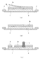
<第1実施形態[図1〜図5]>
本発明の製造方法の第1の実施形態を図1〜図5を参照して説明する。
半導体ウェハ1は、その表面Sに半導体素子の回路などが形成されたパターン面2を有している(図1(a)参照)。このパターン面2には、基材フィルム3aaに粘着剤層3abを設けた表面保護テープ3aの粘着剤層3ab上に、さらにマスク材層3bを設けたマスク一体型表面保護テープ3を貼合し(図1(b)参照)、パターン面2がマスク一体型表面保護テープ3で被覆された半導体ウェハ1を得る(図1(c)参照)。<First Embodiment [FIGS. 1 to 5]>
A first embodiment of the manufacturing method of the present invention will be described with reference to FIGS.
The
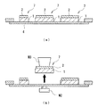
次に、半導体ウェハ1の裏面Bをウェハ研削装置M1で研削し、半導体ウェハ1の厚みを薄くする(図2(a)参照)。その研削した裏面Bにはウェハ固定テープ4を貼り合わせて(図2(b)参照)、リングフレームFに支持固定する(図2(c)参照)。
Next, the back surface B of the
半導体ウェハ1からマスク一体型表面保護テープ3の表面保護テープ3aを剥離するとともにそのマスク材層3bは半導体ウェハ1に残して(図3(a)参照)、マスク材層3bを剥き出しにする(図3(b)参照)。そして、表面Sの側からパターン面2に格子状等に適宜形成された複数のストリート(図示せず)に対してCO2レーザーLを照射して、マスク材層3bのストリートに相当する部分を除去し、半導体ウェハのストリートを開口する(図3(c)参照)。The surface
次に、表面S側からSF6ガスのプラズマP1による処理を行いストリート部分で剥き出しになった半導体ウェハ1をエッチングし(図4(a)参照)、個々のチップ7に分割して個片化する(図4(b)参照)、次いでO2ガスのプラズマP2によってアッシングを行い(図4(c)参照)、表面Sに残ったマスク材層3bを取り除く(図5(a)参照)。そして最後に個片化されたチップ7をピンM2により突き上げコレットM3により吸着してピックアップする(図5(b)参照)。Next, the
ここで、SF6ガスを用いた半導体ウェハのSiのエッチングプロセスはBOSCHプロセスとも呼ばれ、露出したSiと、SF6をプラズマ化して生成したF原子とを反応させ、四フッ化ケイ素(SiF4)として除去するものであり、リアクティブイオンエッチング(RIE)とも呼ばれる。一方、O2プラズマによる除去は、半導体製造プロセス中ではプラズマクリーナーとしても用いられる方法でアッシング(灰化)とも呼ばれ、対有機物除去の手法の一つである。半導体デバイス表面に残った有機物残渣をクリーニングするために行われる。Here, the Si etching process of the semiconductor wafer using SF 6 gas is also referred to as a BOSCH process, and the exposed Si reacts with F atoms generated by converting SF 6 into plasma to produce silicon tetrafluoride (SiF 4 ) And is also called reactive ion etching (RIE). On the other hand, the removal by O 2 plasma is also used as a plasma cleaner in the semiconductor manufacturing process and is called ashing (ashing), and is one of the methods for removing organic matter. This is performed in order to clean the organic residue remaining on the surface of the semiconductor device.
続いて第2実施形態の説明の前に、本発明の製造方法で用いる材料について説明する。これらの材料は、後述する第2実施形態においても好適に用いることができる。
半導体ウェハ1は、片面に半導体素子の回路などが形成されたパターン面2を有するシリコンウェハなどであり、パターン面2は、半導体素子の回路などが形成された面であって、平面視においてストリートを有する。Subsequently, materials used in the manufacturing method of the present invention will be described before the description of the second embodiment. These materials can also be suitably used in the second embodiment described later.
The
マスク一体型表面保護テープ3は、基材フィルム3aa上に粘着剤層3abが設けられ、さらに粘着剤層3ab上にマスク材層が設けられた構成を有し、パターン面2に形成された半導体素子を保護する機能を有する。即ち、後工程のウェハ薄膜化工程ではパターン面2で半導体ウェハ1を支持してウェハの裏面が研削されるために、この研削時の負荷に耐える必要がある。そのため、マスク一体型表面保護テープ3は単なるレジスト膜等とは異なり、パターン面に形成される素子を被覆するだけの厚みがあって、その押圧抵抗は低く、また研削時のダストや研削水などの浸入が起こらないように素子を密着できるだけの密着性が高いものである。
The mask-integrated
マスク一体型表面保護テープ3のうち基材フィルム3aaはプラスチックやゴム等からなり、例えばポリエチレン、ポリプロピレン、エチレン−プロピレン共重合体、ポリブテン−1、ポリ−4−メチルペンテン−1、エチレン−酢酸ビニル共重合体、エチレン−アクリル酸共重合体、アイオノマー等のα−オレフィンの単独重合体または共重合体、あるいはこれらの混合物、ポリエチレンテレフタレート、ポリエチレンナフタレート、ポリフェニレンサルファイド、ポリエーテルイミド、ポリイミド、ポリカーボネート、ポリメチルメタクリレート、ポリウレタン、スチレン−エチレン−ブテン−もしくはペンテン系共重合体等の単体もしくは2種以上を混合させたもの、さらにこれらにこれら以外の樹脂や充填材、添加剤等が配合された樹脂組成物をその材質として挙げることができ、要求特性に応じて適宜に選ぶことができる。低密度ポリエチレンとエチレン酢酸ビニル共重合体の積層体や、ポリプロピレンとポリエチレンテレフタレートの積層体、ポリエチレンテレフタレート、ポリエチレンナフタレートは好適な材質の一つである。
Of the mask-integrated surface
これらの基材フィルム3aaは、一般的な押出し法を用いて製造できる。基材フィルム3aaを種々の樹脂を積層して得る場合には、共押出し法、ラミネート法などで製造される。この際、通常のラミネートフィルムの製法に於いて普通に行われている様に、樹脂と樹脂の間に接着層を設けても良い。この様な基材フィルム3aaの厚さは、強度、伸度等の特性、放射線透過性の観点から20〜200μmが好ましい。 These base film 3aa can be manufactured using a general extrusion method. When the base film 3aa is obtained by laminating various resins, it is manufactured by a coextrusion method, a lamination method, or the like. At this time, an adhesive layer may be provided between the resins, as is usually done in the ordinary laminate film manufacturing method. The thickness of such a base film 3aa is preferably 20 to 200 μm from the viewpoints of properties such as strength and elongation, and radiation transparency.
粘着剤層3abは、マスク材と共に、パターン面に形成される素子の凹凸を吸収してパターン面との密着性を高め、パターン面を保護する役割を担う。マスク一体型表面保護テープをウェハ薄膜化工程(裏面研削工程)の負荷に耐えるものとするために、粘着剤層3abは、ウェハ薄膜化工程においてはマスク材層3bないし基材フィルム3aaとの密着性が高いことが好ましい。一方、ウェハ薄膜化工程後においては、基材フィルム3aaと一体となってマスク材層と剥離されるために、マスク材層との密着性は低いことが好ましい(剥離性が高いことが好ましい)。かかる特性をより高いレベルで実現するために、粘着剤層3abには放射線硬化型の粘着剤を採用することが好ましい。粘着剤層3abを放射線硬化型粘着剤層とすることにより、放射線照射によって粘着剤層が三次元網状化して粘着力が低下するため、ウェハ薄膜化工程後に放射線を照射することによりマスク材層との強固な密着性が解かれてマスク材層から簡単に剥離することが可能となる(この具体的実施形態は後述する)。粘着剤層3abを放射線硬化型粘着剤層とする場合、本発明の製造方法は後述する第2実施形態とすることが好ましい。なお、本発明において粘着剤層3abは放射線硬化型粘着剤に限られず、所望の特性を有する範囲で非放射線硬化型の粘着剤(感圧型粘着剤)を用いてもよく、この場合、本発明の製造方法は上述した第1実施形態とすることが好ましい。
本明細書において「放射線」とは紫外線のような光線や電子線のような電離性放射線の双方を含む意味に用いる、本発明に用いる放射線は紫外線が好ましい。The pressure-sensitive adhesive layer 3ab plays a role of protecting the pattern surface together with the mask material by absorbing the irregularities of the elements formed on the pattern surface to improve the adhesion with the pattern surface. In order to withstand the load of the wafer thinning process (back grinding process) on the mask-integrated surface protection tape, the adhesive layer 3ab is in close contact with the
In the present specification, “radiation” is used to mean both light rays such as ultraviolet rays and ionizing radiations such as electron beams. The radiation used in the present invention is preferably ultraviolet rays.
粘着剤層3abが放射線硬化型粘着剤で構成される場合、アクリル系粘着剤と放射線重合性化合物とを含有してなる粘着剤を好適に用いることができる。
アクリル系粘着剤は、(メタ)アクリル系共重合体、あるいは(メタ)アクリル系共重合体と硬化剤との混合物である。(メタ)アクリル系共重合体は、例えば(メタ)アクリル酸エステルを構成成分として有する共重合体、あるいは(メタ)アクリル酸エステルを構成成分として有する2種以上の共重合体の混合物等が挙げられる。これらの共重合体の重量平均分子量は、通常は30万〜100万程度である。(メタ)アクリル系共重合体の全モノマー成分中、(メタ)アクリル酸エステル成分の割合は70モル%以上が好ましく、80モル%以上がより好ましく、90モル%以上がさらに好ましい。また、(メタ)アクリル系共重合体のモノマー成分中、(メタ)アクリル酸エステル成分の割合が100モル%でない場合、残部のモノマー成分は(メタ)アクリロイル基を重合性基として重合した形態で存在するモノマー成分((メタ)アクリル酸由来の構成成分等)であることが好ましい。また、(メタ)アクリル系共重合体の全モノマー成分中、後述する硬化剤と反応する官能基(例えばヒドロキシ基)を有する(メタ)アクリル酸エステル成分の割合は、1モル%以上が好ましく、2モル%以上がより好ましく、5モル%以上がより好ましく、10モル%以上がより好ましい。また当該(メタ)アクリル酸エステル成分の割合は35モル%以下が好ましく、25モル%以下がより好ましい。また、(メタ)アクリル系共重合体の全モノマー成分中、後述する硬化剤と反応する官能基(例えばヒドロキシ基)を有する構成成分(モノマー成分)の割合は、5モル%以上が好ましく、10モル%以上がより好ましい。当該割合の上限値は35モル%以下が好ましく、25モル%以下がより好ましい。
上記(メタ)アクリル酸エステル成分は、(メタ)アクリル酸アルキルエステル(アルキル(メタ)アクリレートともいう)であることが好ましい。この(メタ)アクリル酸アルキルエステルを構成するアルキル基の炭素数は、1〜20が好ましく、1〜15がより好ましく、1〜12がさらに好ましい。When the pressure-sensitive adhesive layer 3ab is composed of a radiation-curable pressure-sensitive adhesive, a pressure-sensitive adhesive containing an acrylic pressure-sensitive adhesive and a radiation polymerizable compound can be suitably used.
The acrylic pressure-sensitive adhesive is a (meth) acrylic copolymer or a mixture of a (meth) acrylic copolymer and a curing agent. Examples of the (meth) acrylic copolymer include a copolymer having a (meth) acrylic acid ester as a constituent component, or a mixture of two or more kinds of copolymers having a (meth) acrylic acid ester as a constituent component. It is done. The weight average molecular weight of these copolymers is usually about 300,000 to 1,000,000. In all monomer components of the (meth) acrylic copolymer, the proportion of the (meth) acrylic acid ester component is preferably 70 mol% or more, more preferably 80 mol% or more, and further preferably 90 mol% or more. Moreover, in the monomer component of the (meth) acrylic copolymer, when the proportion of the (meth) acrylic acid ester component is not 100 mol%, the remaining monomer component is in a form in which the (meth) acryloyl group is polymerized as a polymerizable group. It is preferable that the monomer component is present (a component derived from (meth) acrylic acid or the like). In addition, in all monomer components of the (meth) acrylic copolymer, the proportion of the (meth) acrylic acid ester component having a functional group (for example, a hydroxy group) that reacts with the curing agent described later is preferably 1 mol% or more. 2 mol% or more is more preferable, 5 mol% or more is more preferable, and 10 mol% or more is more preferable. Further, the proportion of the (meth) acrylic acid ester component is preferably 35 mol% or less, and more preferably 25 mol% or less. In addition, the ratio of the constituent component (monomer component) having a functional group (for example, a hydroxy group) that reacts with the curing agent described later in all monomer components of the (meth) acrylic copolymer is preferably 5 mol% or more. Mole% or more is more preferable. The upper limit of the ratio is preferably 35 mol% or less, and more preferably 25 mol% or less.
The (meth) acrylic acid ester component is preferably a (meth) acrylic acid alkyl ester (also referred to as an alkyl (meth) acrylate). 1-20 are preferable, as for carbon number of the alkyl group which comprises this (meth) acrylic-acid alkylester, 1-15 are more preferable, and 1-12 are more preferable.
硬化剤は、(メタ)アクリル系共重合体が有する官能基と反応させて粘着力及び凝集力を調整するために用いられるものである。例えば、1,3−ビス(N,N−ジグリシジルアミノメチル)シクロヘキサン、1,3−ビス(N,N−ジグリシジルアミノメチル)トルエン、1,3−ビス(N,N−ジグリシジルアミノメチル)ベンゼン、N,N,N,N’−テトラグリシジル−m−キシレンジアミンなどの分子中に2個以上のエポキシ基を有するエポキシ化合物、2,4−トリレンジイソシアネート、2,6−トリレンジイソシアネート、1,3−キシリレンジイソシアネート、1,4−キシレンジイソシアネート、ジフェニルメタン−4,4’−ジイソシアネートなどの分子中に2個以上のイソシアネート基を有するイソシアネート系化合物、テトラメチロール−トリ−β−アジリジニルプロピオネート、トリメチロール−トリ−β−アジリジニルプロピオネート、トリメチロールプロパン−トリ−β−アジリジニルプロピオネート、トリメチロールプロパン−トリ−β−(2−メチルアジリジン)プロピオネートなどの分子中に2個以上のアジリジニル基を有するアジリジン系化合物等が挙げられる。硬化剤の添加量は、所望の粘着力に応じて調整すればよく、(メタ)アクリル系共重合体100質量部に対して0.1〜5.0質量部が適当である。本発明に用いるマスク一体型表面保護テープの粘着剤層において、硬化剤は(メタ)アクリル系共重合体と反応した状態にある。 A hardening | curing agent is used in order to make it react with the functional group which a (meth) acrylic-type copolymer has, and to adjust adhesive force and cohesion force. For example, 1,3-bis (N, N-diglycidylaminomethyl) cyclohexane, 1,3-bis (N, N-diglycidylaminomethyl) toluene, 1,3-bis (N, N-diglycidylaminomethyl) ) Epoxy compounds having two or more epoxy groups in the molecule such as benzene, N, N, N, N′-tetraglycidyl-m-xylenediamine, 2,4-tolylene diisocyanate, 2,6-tolylene diisocyanate , 1,3-xylylene diisocyanate, 1,4-xylene diisocyanate, diphenylmethane-4,4′-diisocyanate and the like, an isocyanate compound having two or more isocyanate groups in the molecule, tetramethylol-tri-β-aziridini Lupropionate, trimethylol-tri-β-aziridinylpropionate, Examples thereof include aziridine compounds having two or more aziridinyl groups in the molecule, such as dimethylolpropane-tri-β-aziridinylpropionate and trimethylolpropane-tri-β- (2-methylaziridine) propionate. . What is necessary is just to adjust the addition amount of a hardening | curing agent according to desired adhesive force, and 0.1-5.0 mass parts is suitable with respect to 100 mass parts of (meth) acrylic-type copolymers. In the pressure-sensitive adhesive layer of the mask-integrated surface protective tape used in the present invention, the curing agent is in a state of reacting with the (meth) acrylic copolymer.
上記放射線重合性化合物としては、放射線の照射によって三次元網状化しうる、分子内に光重合性炭素−炭素二重結合を少なくとも2個以上有する低分量化合物が広く用いられる。具体的には、トリメチロールプロパントリアクリレート、テトラメチロールメタンテトラアクリレート、ペンタエリスリトールトリアクリレート、ペンタエリスリトールテトラアクリレート、ジペンタエリスリトールモノヒドロキシペンタアクリレート、ジペンタエリスリトールヘキサアクリレート、1,4−ブチレングリコールジアクリレート、1,6−ヘキサンジオールジアクリレート、ポリエチレングリコールジアクリレートや、オリゴエステルアクリレート等のアクリレート系化合物を広く適用可能である。 As the radiation-polymerizable compound, low-volume compounds having at least two photopolymerizable carbon-carbon double bonds in the molecule that can be three-dimensionally reticulated by irradiation with radiation are widely used. Specifically, trimethylolpropane triacrylate, tetramethylolmethane tetraacrylate, pentaerythritol triacrylate, pentaerythritol tetraacrylate, dipentaerythritol monohydroxypentaacrylate, dipentaerythritol hexaacrylate, 1,4-butylene glycol diacrylate, Acrylate compounds such as 1,6-hexanediol diacrylate, polyethylene glycol diacrylate, and oligoester acrylate are widely applicable.
また、上記アクリレート系化合物のほかに、ウレタンアクリレート系オリゴマーを用いる事も出来る。ウレタンアクリレート系オリゴマーは、ポリエステル型またはポリエーテル型などのポリオール化合物と、多価イソシアナート化合物(例えば、2,4−トリレンジイソシアナート、2,6−トリレンジイソシアナート、1,3−キシリレンジイソシアナート、1,4−キシリレンジイソシアナート、ジフェニルメタン4,4−ジイソシアナートなど)を反応させて得られる末端イソシアナートウレタンプレポリマーに、ヒドロキシ基を有するアクリレートあるいはメタクリレート(例えば、2−ヒドロキシエチルアクリレート、2−ヒドロキシエチルメタクリレート、2−ヒドロキシプロピルアクリレート、2−ヒドロキシプロピルメタクリレート、ポリエチレングリコールアクリレート、ポリエチレングリコールメタクリレートなど)を反応させて得られる。
In addition to the above acrylate compounds, urethane acrylate oligomers can also be used. The urethane acrylate oligomer includes a polyol compound such as a polyester type or a polyether type, and a polyvalent isocyanate compound (for example, 2,4-tolylene diisocyanate, 2,6-tolylene diisocyanate, 1,3-xylylene diene). A terminal isocyanate urethane prepolymer obtained by reacting isocyanate, 1,4-xylylene diisocyanate,
放射線硬化型粘着剤中のアクリル系粘着剤と放射線重合性化合物との配合比としては、アクリル系粘着剤100質量部に対して放射線重合性化合物を50〜200質量部、好ましくは50〜150質量部の範囲で配合されるのが望ましい。この配合比の範囲である場合、放射線照射後に粘着剤層の粘着力を大きく低下させることが可能となる。 As a compounding ratio of the acrylic pressure-sensitive adhesive and the radiation-polymerizable compound in the radiation-curable pressure-sensitive adhesive, the radiation-polymerizable compound is 50 to 200 parts by weight, preferably 50 to 150 parts by weight with respect to 100 parts by weight of the acrylic pressure-sensitive adhesive. It is desirable to blend in the range of parts. When the blending ratio is in this range, the adhesive strength of the pressure-sensitive adhesive layer can be greatly reduced after irradiation.
また、粘着剤層3abに用いる放射線硬化型粘着剤として、上記(メタ)アクリル系共重合体自体を放射線重合性とした、放射線重合性(メタ)アクリル系共重合体を用いることも好ましい。この場合において、放射線硬化型粘着剤は硬化剤を含んでいてもよい。
放射線重合性(メタ)アクリル系共重合体は、共重合体の分子中に、放射線、特に紫外線照射で重合反応することが可能な反応性の基を有する共重合体である。このような反応性の基としては、エチレン性不飽和基、すなわち、炭素−炭素二重結合を有する基が好ましい。かかる基の例として、ビニル基、アリル基、スチリル基、(メタ)アクリロイルオキシ基、(メタ)アクリロイルアミノ基などが挙げられる。
上記反応性基の共重合体中への導入は、例えば、ヒドロキシ基を有する共重合体と、ヒドロキシ基と反応する基(例えば、イソシアネート基)を有し、かつ上記反応性基を有する化合物〔(代表的には、2−(メタ)アクリロイルオキシエチルイソシアネート〕とを反応させることにより行うことができる。
また、上記放射線重合性(メタ)アクリル系共重合体を構成する全モノマー成分中、上記の反応性の基を有するモノマー成分の割合は2〜40モル%が好ましく、5〜30モル%がより好ましく、10〜30モル%がさらに好ましい。Moreover, it is also preferable to use the radiation-polymerizable (meth) acrylic copolymer in which the (meth) acrylic copolymer itself is radiation-polymerizable as the radiation-curable pressure-sensitive adhesive used for the pressure-sensitive adhesive layer 3ab. In this case, the radiation curable pressure-sensitive adhesive may contain a curing agent.
The radiation-polymerizable (meth) acrylic copolymer is a copolymer having a reactive group capable of undergoing a polymerization reaction upon irradiation with radiation, particularly ultraviolet rays, in the copolymer molecule. As such a reactive group, an ethylenically unsaturated group, that is, a group having a carbon-carbon double bond is preferable. Examples of such groups include vinyl groups, allyl groups, styryl groups, (meth) acryloyloxy groups, (meth) acryloylamino groups, and the like.
The introduction of the reactive group into the copolymer includes, for example, a copolymer having a hydroxy group and a compound having a group that reacts with the hydroxy group (for example, an isocyanate group) and having the reactive group [ (Typically, it can be carried out by reacting with 2- (meth) acryloyloxyethyl isocyanate).
Moreover, 2-40 mol% is preferable and, as for the ratio of the monomer component which has said reactive group in all the monomer components which comprise the said radiation polymerizable (meth) acrylic-type copolymer, 5-30 mol% is more. Preferably, 10 to 30 mol% is more preferable.
また、放射線により粘着剤層3abを重合硬化させる場合には、光重合開始剤、例えばイソプロピルベンゾインエーテル、イソブチルベンゾインエーテル、ベンゾフェノン、ミヒラーズケトン、クロロチオキサントン、ベンジルメチルケタール、α−ヒドロキシシクロヘキシルフェニルケトン、2−ヒドロキシメチルフェニルプロパン等を用いることが出来る。これらのうち少なくとも1種類を粘着剤層に添加することにより、効率よく重合反応を進行させることが出来る。 When the adhesive layer 3ab is polymerized and cured by radiation, a photopolymerization initiator such as isopropyl benzoin ether, isobutyl benzoin ether, benzophenone, Michler's ketone, chlorothioxanthone, benzyl methyl ketal, α-hydroxycyclohexyl phenyl ketone, 2- Hydroxymethylphenylpropane or the like can be used. By adding at least one of these to the pressure-sensitive adhesive layer, the polymerization reaction can proceed efficiently.
上記粘着剤層3abは、さらに光増感剤、従来公知の粘着付与剤、軟化剤、酸化防止剤等を含有していてもよい。 The pressure-sensitive adhesive layer 3ab may further contain a photosensitizer, a conventionally known tackifier, softener, antioxidant, and the like.
上記粘着剤層3abとして、特開2014−192204号公報の段落番号0036〜0055に記載されている形態を採用することも好ましい。 As the pressure-sensitive adhesive layer 3ab, it is also preferable to adopt the form described in paragraph numbers 0036 to 0055 of JP-A-2014-192204.
粘着剤層3abの厚さは、パターン面2に形成された素子等の保護能をより高め、またパターン面への密着性をより高め、且つアッシング処理による除去性をより高める観点から、5〜100μmが好ましく、10〜100μmがより好ましく、2〜50μmがさらに好ましい。なお、デバイスの種類にもよるが、パターン表面の凹凸は概ね数μm〜15μm程度であるため、粘着剤層3abの厚さは5〜30μmがより好ましい。
The thickness of the pressure-sensitive adhesive layer 3ab is 5 to 5 from the viewpoint of further improving the protection ability of the elements and the like formed on the
マスク材層3bには、非放射線硬化型である、いわゆる感圧型の粘着剤が好適に用いられる。この感圧型の粘着剤としては、上述した、(メタ)アクリル系共重合体と硬化剤との混合物を好適に用いることができる。
また、マスク材層は後述するエッチングレート特性を有することも好ましい。この場合、マスク材層3bとして、放射線硬化型粘着剤を用いることも好ましい。
マスク材層3bの厚みは、パターン表面への追従性及びプラズマによる除去性の観点から、1〜50μmが好ましく、5〜20μmがより好ましい。For the
The mask material layer preferably has an etching rate characteristic described later. In this case, it is also preferable to use a radiation curable adhesive as the
The thickness of the
ウェハ固定テープ4は、半導体ウェハ1を保持し、プラズマダイシング工程にさらされても耐えうるプラズマ耐性が必要である。またピックアップ工程においては良好なピックアップ性や場合によってはエキスパンド性等も要求されるものである。こうしたウェハ固定テープ4には、上記表面保護テープ3aと同様のテープを用いることができる。また一般的にダイシングテープと称される従来のプラズマダイシング方式で利用される公知のダイシングテープを用いることができる。また、ピックアップ後のダイボンディング工程への移行を容易にするために、粘着剤層と基材フィルムとの間にダイボンディング用接着剤を積層したダイシングダイボンディングテープを用いることもできる。
The
マスク材層3bを切断するレーザー照射には、紫外線または赤外線のレーザー光を照射するレーザー照射装置を用いることができる。このレーザー光照射装置は、半導体ウェハ1のストリートに沿って移動可能にレーザー照射部が配設されており、マスク材層3bを除去するために適切に制御された出力のレーザーを照射できる。なかでもCO2レーザーは数W〜数十Wの大出力を得ることが可能であり、本発明に好適に利用できる。For the laser irradiation for cutting the
プラズマダイシングおよびプラズマアッシングを行うにはプラズマエッチング装置を用いることができる。プラズマエッチング装置は、半導体ウェハ1に対してドライエッチングを行い得る装置であって、真空チャンバ内に密閉処理空間をつくり、高周波側電極に半導体ウェハ1が載置され、その高周波側電極に対向して設けられたガス供給電極側からプラズマ発生用ガスが供給されるものである。高周波側電極に高周波電圧が印加されればガス供給電極と高周波側電極との間にプラズマが発生するため、このプラズマを利用する。発熱する高周波電極内には冷媒を循環させて、プラズマの熱による半導体ウェハ1の昇温を防止している。
A plasma etching apparatus can be used to perform plasma dicing and plasma ashing. The plasma etching apparatus is an apparatus capable of performing dry etching on the
上記半導体チップの製造方法(半導体ウェハの処理方法)によれば、パターン面を保護する表面保護テープにプラズマダイシングにおけるマスク機能を持たせたことで、従来のプラズマダイシングプロセスで用いられていたレジストを設けるためのフォトリソ工程等が不要となる。特に表面保護テープを用いたため、マスクの形成に印刷や転写等の高度な位置合わせが要求される技術が不要で簡単に半導体ウェハ表面に貼合でき、レーザー装置により簡単にマスクを形成できる。
また、マスク材層3bをO2プラズマで除去できるため、プラズマダイシングを行う装置と同じ装置でマスク部分の除去ができる。加えてパターン面2側(表面S側)からプラズマダイシングを行うため、ピッキング作業前にチップの上下を反転させる必要がない。これらの理由から設備を簡易化でき、プロセスコストを大幅に抑えることができる。According to the above semiconductor chip manufacturing method (semiconductor wafer processing method), the resist used in the conventional plasma dicing process can be obtained by providing the surface protection tape for protecting the pattern surface with a mask function in plasma dicing. A photolithographic process or the like for providing is unnecessary. In particular, since a surface protection tape is used, a technique that requires high-level alignment such as printing and transfer is not required for forming a mask, and it can be easily bonded to the surface of a semiconductor wafer, and a mask can be easily formed by a laser device.
Further, since the
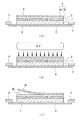
<第2実施形態[図6]>
第2実施形態では第1実施形態における表面保護テープ3aを剥離する工程の前に、マスク一体型表面保護テープ3に紫外線等の放射線を照射して粘着剤層を硬化させる工程を含む点で第1実施形態と異なる。その他の工程は第1実施形態と同じである。<Second Embodiment [FIG. 6]>
The second embodiment includes the step of curing the pressure-sensitive adhesive layer by irradiating the mask-integrated surface
即ち、半導体ウェハ1の表面S側にはマスク一体型表面保護テープ3を貼合し、半導体ウェハ1の研削した裏面B側にはウェハ固定テープ4を貼合し、リングフレームFに支持固定した(図2(c)、図6(a)参照)後、表面S側からマスク一体型表面保護テープ3に向けて紫外線(UV)を照射する(図6(b)参照)。そして、マスク一体型表面保護テープ3の粘着剤層3abを硬化させた後、表面保護テープ3aを取り除いて(図6(c)参照)マスク材層3bを剥き出しにする。そしてレーザーLによりストリートに相当する部分のマスク材層3bを切除する工程に移る。
That is, the mask-integrated type
第2実施形態で用いるマスク一体型表面保護テープは、第1実施形態で示したマスク一体型表面保護テープ3の中でも紫外線等の放射線で硬化可能な材質を粘着剤層3abに用いたものである。
粘着剤層3abを紫外線等で硬化させることにより、表面保護テープ3aとマスク材層3bとの剥離が容易になる。The mask-integrated surface protective tape used in the second embodiment uses a material curable with radiation such as ultraviolet rays for the adhesive layer 3ab among the mask-integrated surface
By curing the pressure-sensitive adhesive layer 3ab with ultraviolet rays or the like, the
続いて本発明の製造方法に用いるのに好適なマスク一体型表面保護テープの一実施形態(以下、「本発明のマスク一体型表面保護テープ」ともいう。)について、以下により詳細に説明するが、本発明の製造方法に用いるマスク一体型表面保護テープは下記の実施形態に限定されるものではなく、上記で説明した形態のマスク一体型表面保護テープを広く用いることができる。 Subsequently, an embodiment of a mask-integrated surface protective tape suitable for use in the production method of the present invention (hereinafter also referred to as “mask-integrated surface protective tape of the present invention”) will be described in more detail below. The mask-integrated surface protective tape used in the production method of the present invention is not limited to the following embodiment, and the mask-integrated surface protective tape having the above-described form can be widely used.
<本発明のマスク一体型表面保護テープ>
本発明のマスク一体型表面保護テープ3は、基材フィルム3aa上に粘着剤層3abが形成された表面保護テープ3aの、さらに粘着剤層3ab上にマスク材層3bが形成されたテープであって、上記マスク材層3bのSF6プラズマによるエッチングレート(EF)が、O2プラズマによるエッチングレート(EO2)よりも低い。
本発明のマスク一体型表面保護テープにおいて、基材フィルム、粘着剤層、マスク材層は単層構造でも2層以上の複層構造でもよい。粘着剤層及びマスク材層は好ましくは単層構造である。本発明のマスク一体型表面保護テープにおいて、基材フィルム及び粘着剤層の構成は、上述した本発明の製造方法において説明した形態を適用することができる。本発明のマスク一体型表面保護テープのマスク材層の構成について以下に説明する。<Mask integrated surface protection tape of the present invention>
The mask-integrated surface
In the mask-integrated surface protective tape of the present invention, the base film, the pressure-sensitive adhesive layer, and the mask material layer may have a single layer structure or a multilayer structure of two or more layers. The pressure-sensitive adhesive layer and the mask material layer preferably have a single layer structure. In the mask-integrated surface protective tape of the present invention, the configuration described in the above-described production method of the present invention can be applied to the base film and the pressure-sensitive adhesive layer. The structure of the mask material layer of the mask-integrated surface protection tape of the present invention will be described below.
(マスク剤層3b)
本発明のマスク一体型表面保護テープにおいて、マスク材層3bは、パターン面2への貼着に際し半導体素子等を傷つけにくく、また、その除去の際に半導体素子等の破損や表面への粘着剤残留を生じにくいものである。さらに、本発明においては、マスク材層3bは、SF6プラズマによるエッチングレート(EF)が、O2プラズマによるエッチングレート(EO2)よりも低いため、回路面に形成されたマスクは、プラズマダイシングに際しマスクとして機能する耐プラズマ性を有し、かつ、アッシングによって形成されたマスクをより確実に除去することができる。(
In the mask-integrated surface protective tape of the present invention, the
本発明のマスク一体型表面保護テープにおいて、マスク剤層のSF6プラズマによるエッチングレート(EF)は、実施例に記載のように、SF6ガスプラズマによりSiウェハを15μm/分のエッチングレートでエッチングする条件での、マスク剤層のエッチングレートを言う。
また、本発明のマスク一体型表面保護テープにおいて、マスク剤層のO2プラズマによるエッチングレート(EO2)は、実施例に記載される、O2ガスプラズマによりマスク剤層aを1μm/分のエッチングレートでエッチングする条件での、マスク剤層のエッチングレートを言う。In the mask-integrated surface protective tape of the present invention, the etching rate (E F ) of the mask agent layer by SF 6 plasma is set to 15 μm / min by etching the Si wafer by SF 6 gas plasma as described in the Examples. It refers to the etching rate of the mask agent layer under the etching conditions.
Further, in the mask-integrated surface protection tape of the present invention, the etching rate (E O2) by O 2 plasma mask adhesive layer, as described in the Examples by O 2 gas plasma mask material layer a of 1 [mu] m / min It means the etching rate of the mask agent layer under the condition of etching at the etching rate.
さらに、本発明のマスク一体型表面保護テープにおいて、SF6プラズマによるエッチングレート(EF)に対するO2プラズマによるエッチングレート(EO2)の比であるEO2/EFは、2.0以上であることが好ましく、4.0以上であることがより好ましく、6.0以上であることがさらに好ましい。上限値の制限は特にないが、8.0以下であることが現実的である。
なお、マスク剤層が放射線重合型のマスク材である場合には、上記のエッチングレートは、放射線重合された後のマスク剤層についてのエッチングレートを意味する。Furthermore, in the mask-integrated surface protective tape of the present invention, E O2 / E F , which is the ratio of the etching rate (E O2 ) by O 2 plasma to the etching rate (E F ) by SF 6 plasma, is 2.0 or more. Preferably, it is 4.0 or more, more preferably 6.0 or more. Although there is no particular limitation on the upper limit value, it is realistic to be 8.0 or less.
When the mask agent layer is a radiation polymerization type mask material, the above etching rate means the etching rate for the mask agent layer after being subjected to radiation polymerization.
さらに、本発明のマスク一体型表面保護テープにおいて、マスク材層3bは、波長10μmでの光線透過率(以下、光線透過率10μmとも称す。)が80%以下であり、波長350〜700nmでの可視光線透過率(以下、可視光線透過率350−700μmとも称す。)が50%以上であることが好ましい。
光線透過率10μmは、79%以下であることがより好ましく、75%以下であることがさらに好ましい。下限値の制限は特にないが、30%以上であることが現実的である。
可視光線透過率350−700μmは、70%以上であることがより好ましく、90%以上であることがさらに好ましい。上限値の制限は特にないが、100%以下であることが好ましい。Furthermore, in the mask-integrated surface protective tape of the present invention, the
The light transmittance of 10 μm is more preferably 79% or less, and further preferably 75% or less. Although there is no restriction | limiting in particular of a lower limit, it is realistic that it is 30% or more.
The visible light transmittance of 350 to 700 μm is more preferably 70% or more, and further preferably 90% or more. The upper limit is not particularly limited, but is preferably 100% or less.
光線透過率10μmが上記好ましい範囲内にあることで、マスク材層のうち、半導体ウェハのストリートに相当する部分を、CO2レーザーにより効率的に切断することができる。
また、可視光線透過率350−700μmが上記好ましい範囲内にあることで、半導体ウェハのパターン面2を適切に認識することができ、ストリート開口する際の誤認識を防止することができる。
上記光線透過率は、後述の実施例に記載の方法により測定される。When the light transmittance of 10 μm is within the above preferable range, the portion corresponding to the street of the semiconductor wafer in the mask material layer can be efficiently cut with a CO 2 laser.
Further, since the visible light transmittance of 350 to 700 μm is within the above preferable range, the
The said light transmittance is measured by the method as described in the below-mentioned Example.
また、本発明のマスク一体型表面保護テープ3は、パターン面2を保護する機能を有する。即ち、後工程のウェハ薄膜化工程ではパターン面2で半導体ウェハ1を支持してウェハの裏面が研削されるために、この研削時の負荷に耐える必要がある。そのため、本発明のマスク一体型表面保護テープ3は単なるレジスト膜等とは異なり、パターン面に形成される素子を被覆するだけの厚みがあって、その押圧抵抗は低く、また研削時のダストや研削水などの浸入が起こらないように素子を密着できるだけの密着性が高いものである。
Further, the mask-integrated surface
本発明のマスク一体型表面保護テープにおいて、マスク材層3bには上記各種の性能が求められるため、マスク材層3bにはこうした性質を有する非硬化性のマスク材を用いることができる。また、好ましくは放射線、より好ましくは紫外線照射によりマスク材層が三次元網状化を呈し、アッシングによりマスク材層の残留物が生じ難い、紫外線硬化型、あるいは電子線のような電離性放射線硬化型等の放射線重合型のマスク材を用いることができる。
In the mask-integrated surface protection tape of the present invention, the
こうしたマスク材としては、アクリル系粘着剤や、このアクリル系粘着剤と放射線重合性化合物とを含有してなるマスク材を好適に用いることができる。
上記アクリル系粘着剤は、(メタ)アクリル系共重合体、あるいは(メタ)アクリル系共重合体と硬化剤との混合物であり、前述の粘着剤層で記載するアクリル系粘着剤を好適に用いることができる。
なお、密着性の観点から、(メタ)アクリル系共重合体の全モノマー成分中、硬化剤と反応する官能基(例えば、ヒドロキシ基)を有する(メタ)アクリル酸エステル成分の割合は、0.1モル%以上が好ましく、0.5モル%以上がより好ましい。上限値は、20モル%以下であることが好ましく、15モル%以下であることがより好ましい。(メタ)アクリル系共重合体の質量平均分子量は、10万〜100万程度が好ましい。As such a mask material, an acrylic pressure-sensitive adhesive or a mask material comprising this acrylic pressure-sensitive adhesive and a radiation polymerizable compound can be suitably used.
The acrylic pressure-sensitive adhesive is a (meth) acrylic copolymer or a mixture of a (meth) acrylic copolymer and a curing agent, and the acrylic pressure-sensitive adhesive described in the pressure-sensitive adhesive layer is preferably used. be able to.
From the viewpoint of adhesion, the ratio of the (meth) acrylic acid ester component having a functional group (for example, a hydroxy group) that reacts with the curing agent in the total monomer components of the (meth) acrylic copolymer is 0.00. 1 mol% or more is preferable and 0.5 mol% or more is more preferable. The upper limit is preferably 20 mol% or less, and more preferably 15 mol% or less. The mass average molecular weight of the (meth) acrylic copolymer is preferably about 100,000 to 1,000,000.
本発明のマスク一体型表面保護テープにおいて、マスク材層3bとしては、放射線で硬化する放射線硬化型粘着剤や、放射線で硬化しない感圧型粘着剤を好適に用いることができる。
上記放射線硬化型粘着剤としては、上記アクリル系粘着剤と、分子内に1または2個の光重合性炭素−炭素二重結合を有するアクリレート化合物とを含有してなる粘着剤が好適である。上記放射線硬化型粘着剤中、分子内に1または2個の光重合性炭素−炭素二重結合を有するアクリレート化合物の含有量は15質量%以上が好ましく、15〜70質量%がより好ましく、15〜65質量%がさらに好ましい。また、分子内に1または2個の光重合性炭素−炭素二重結合を有するアクリレート化合物は、分子内に1個の光重合性炭素−炭素二重結合を有するアクリレート化合物であることが好ましい。
上記分子内に1または2個の光重合性炭素−炭素二重結合を有するアクリレート化合物は、具体的には、2−ヒドロキシ−3−フェノキシプロピルアクリレート、1,4−ブチレングリコールジアクリレート、1,6−ヘキサンジオールジアクリレート、ポリエチレングリコールジアクリレート等を広く適用可能である。
また、分子内に1または2個の光重合性炭素−炭素二重結合を有する、ウレタンアクリレートオリゴマーを好適に用いる事ができ、前述の粘着剤層に記載する方法で得られるウレタンアクリレートオリゴマーを好ましく用いることができる。In the mask-integrated surface protective tape of the present invention, as the
As the radiation curable pressure-sensitive adhesive, a pressure-sensitive adhesive comprising the acrylic pressure-sensitive adhesive and an acrylate compound having one or two photopolymerizable carbon-carbon double bonds in the molecule is suitable. In the radiation curable pressure-sensitive adhesive, the content of the acrylate compound having one or two photopolymerizable carbon-carbon double bonds in the molecule is preferably 15% by mass or more, more preferably 15 to 70% by mass, -65 mass% is further more preferable. The acrylate compound having 1 or 2 photopolymerizable carbon-carbon double bonds in the molecule is preferably an acrylate compound having 1 photopolymerizable carbon-carbon double bond in the molecule.
Specific examples of the acrylate compound having 1 or 2 photopolymerizable carbon-carbon double bonds in the molecule include 2-hydroxy-3-phenoxypropyl acrylate, 1,4-butylene glycol diacrylate, 1, 6-hexanediol diacrylate, polyethylene glycol diacrylate and the like are widely applicable.
Moreover, the urethane acrylate oligomer which has a 1 or 2 photopolymerizable carbon-carbon double bond in a molecule | numerator can be used conveniently, The urethane acrylate oligomer obtained by the method described in the above-mentioned adhesive layer is preferable. Can be used.
上記放射線硬化型粘着剤中のアクリル系粘着剤と、分子内に1または2個の光重合性炭素−炭素二重結合を有するアクリレート化合物との配合比としては、アクリル系粘着剤100質量部に対して、分子内に1または2個の光重合性炭素−炭素二重結合を有するアクリレート化合物を10〜250質量部、好ましくは15〜200質量部の範囲で配合されるのが好ましい。上記上限値以下であると、裏面研削時にマスク材層が過度に変形することなく、ウェハの破損をより効果的に防止することができる。 The blending ratio of the acrylic pressure-sensitive adhesive in the radiation curable pressure-sensitive adhesive and the acrylate compound having one or two photopolymerizable carbon-carbon double bonds in the molecule is 100 parts by weight of the acrylic pressure-sensitive adhesive. On the other hand, the acrylate compound having one or two photopolymerizable carbon-carbon double bonds in the molecule is preferably blended in an amount of 10 to 250 parts by mass, preferably 15 to 200 parts by mass. If it is not more than the above upper limit value, the mask material layer will not be excessively deformed during back surface grinding, and damage to the wafer can be more effectively prevented.
また、本発明のマスク一体型表面保護テープにおいて、マスク剤層には、前述の粘着剤層における放射線重合性(メタ)アクリル酸エステル共重合体、光重合開始剤、その他の含有成分(光増感剤、従来公知の粘着付与剤、軟化剤、酸化防止剤等)を好ましく適用することができる。 In the mask-integrated surface protective tape of the present invention, the mask agent layer includes a radiation-polymerizable (meth) acrylic acid ester copolymer, a photopolymerization initiator, and other components (photosensitizer) in the aforementioned pressure-sensitive adhesive layer. Sensitizers, conventionally known tackifiers, softeners, antioxidants, etc.) can be preferably applied.
本発明のマスク一体型表面保護テープにおいて、マスク材層3bの厚さは、パターン面2に形成された素子等の保護能をより高め、またパターン面への密着性をより高めることでSF6ガスの侵入を防止し、且つアッシング処理による除去性をより高める観点から、5〜100μmが好ましく、5〜30μmがより好ましい。なお、デバイスの種類にもよるが、パターン表面の凹凸は概ね数μm〜15μm程度であるため、マスク材層3bの厚さは5〜30μmがより好ましい。In the mask-integrated surface protective tape of the present invention, the thickness of the
上記各実施形態は本発明の一例であり、こうした形態に限定されるものではなく、本発明の趣旨に反しない限度において、各プロセスにおける公知のプロセスの付加や削除、変更等を行い得るものである。 Each of the above-described embodiments is an example of the present invention, and is not limited to such a form, and can add, delete, and change a known process in each process as long as not departing from the spirit of the present invention. is there.
以下、実施例に基づき本発明をさらに詳細に説明するが、本発明はこれに限定されるものでない。 EXAMPLES Hereinafter, although this invention is demonstrated further in detail based on an Example, this invention is not limited to this.
[参考例1] マスク一体型表面保護テープの作製−1
<表面保護テープ3aの調製>
2−エチルヘキシルアクリレート:80mol%、アクリル酸メチル:1mol%、2-ヒドロキシエチルアクリレート:19mol%の各モノマー由来の構成成分からなるアクリルポリマー(ランダムポリマー)に対し、分子中にエチレン性不飽和結合(光反応性基)とイソシアネート基を有する2−イソシアナトエチルメタクリレート(MOI、昭和電工製)を反応させ、分子中にエチレン性不飽和結合を有するアクリルポリマーA1(Mw:80万、酸価:12mgKOH/g、水酸基価:43mgKOH/g、二重結合当量:0.9eq)を得た。
前記アクリルポリマーA1の100質量部に対し、イソシアネート硬化剤(商品名:L‐45、東ソー株式会社製)を2.0質量部、光重合開始剤(エザキュア KIP 100F、Lamberti製)を5.0質量部配合し、粘着剤組成物Aを得た。[Reference Example 1] Production of mask-integrated surface protective tape-1
<Preparation of
2-ethylhexyl acrylate: 80 mol%, methyl acrylate: 1 mol%, 2-hydroxyethyl acrylate: 19 mol% An acrylic polymer (random polymer) composed of components derived from each monomer, and an ethylenically unsaturated bond ( Acrylic polymer A1 (Mw: 800,000, acid value: 12 mgKOH) having an ethylenically unsaturated bond in the molecule by reacting 2-isocyanatoethyl methacrylate (MOI, manufactured by Showa Denko) having an isocyanate group with a photoreactive group) / G, hydroxyl value: 43 mgKOH / g, double bond equivalent: 0.9 eq).
With respect to 100 parts by mass of the acrylic polymer A1, 2.0 parts by mass of an isocyanate curing agent (trade name: L-45, manufactured by Tosoh Corporation) and 5.0% of a photopolymerization initiator (Ezacure KIP 100F, manufactured by Lamberti) An adhesive composition A was obtained by blending parts by mass.
LDPE(低密度ポリエチレン)樹脂(ニポロンハード205、東ソー株式会社製)とEVA(エチレン酢酸ビニル共重合体)樹脂(ウルトラセン540、東ソー株式会社製)とを用いて、押出法により厚さが110μmとなるように製膜し、2層構造の基材フィルム3aaを調製した。
上記粘着剤組成物Aを離型フィルム上に塗工し、乾燥して形成された粘着剤層を上記基材フィルム3aaのEVA層上に貼り合わせ、転写し、厚さ20μmの放射線硬化型の粘着剤層3abを形成し、表面保護テープ3aを得た。Using an LDPE (low density polyethylene) resin (Nipolon Hard 205, manufactured by Tosoh Corporation) and EVA (ethylene vinyl acetate copolymer) resin (Ultrasen 540, manufactured by Tosoh Corporation), the thickness is 110 μm by an extrusion method. As a result, a base film 3aa having a two-layer structure was prepared.
The pressure-sensitive adhesive composition A is applied onto a release film, and the pressure-sensitive adhesive layer formed by drying is bonded onto the EVA layer of the base film 3aa, transferred, and a radiation-curing type having a thickness of 20 μm. An adhesive layer 3ab was formed to obtain a surface
<マスク一体型表面保護テープ3の調製>
ブチルアクリレート:95mol%、アクリル酸メチル:5mol%の各モノマー由来の構成成分からなるアクリルポリマーA2(ランダムポリマー、Mw:100万、酸価:23mgKOH/g、水酸基価:0mgKOH/g):100質量部に対し、エポキシ硬化剤(Tetrad−C、三菱ガス化学製)を2.0質量部配合して、マスク材組成物Aを得た。このマスク材組成物Aを用いて、乾燥後の厚さが10μmとなるように前記表面保護テープ3aの粘着剤層3ab側に成膜して感圧型粘着剤層であるマスク材層3bを形成し、マスク一体型表面保護テープ3を得た。<Preparation of mask-integrated surface
Acrylic polymer A2 (Random polymer, Mw: 1,000,000, acid value: 23 mgKOH / g, hydroxyl value: 0 mgKOH / g): 100 masses consisting of constituents derived from each monomer of butyl acrylate: 95 mol% and methyl acrylate: 5 mol% The mask material composition A was obtained by blending 2.0 parts by mass of an epoxy curing agent (Tetrad-C, manufactured by Mitsubishi Gas Chemical) with respect to the parts. Using this mask material composition A, a film is formed on the pressure-sensitive adhesive layer 3ab side of the surface
[実施例1] 半導体チップの製造−1
得られたマスク一体型表面保護テープ3を、テープ貼合装置(商品名:DR−3000II、日東精機株式会社製)を用いてシリコンウェハ(直径8インチ)に貼り合わせた。マスク一体型表面保護テープ3を貼り合わせたウェハを、裏面研削装置(商品名:DGP8760、株式会社DISCO製)を用いて厚さが50μmになるまで研削し、その際のウェハの割れの有無を、目視及び顕微鏡により調べた。
研削されたウェハの裏面側にUV硬化型のウェハ固定テープ4(商品名:UC−353EP−110、古河電気工業株式会社製)を貼り合わせ、リングフレームを用いて支持固定した。次いでマスク一体型表面保護テープ3側から紫外線を照射し、その後マスク材層3bを残して表面保護テープ3aを引き剥がした。剥き出しになったマスク材層3bの上からシリコンウェハのストリート部分に沿ってCO2レーザーを照射し、当該部分のマスク材層3bを除去してストリート部分を開口した。
その後、プラズマ発生用ガスとしてSF6ガスを用い、0.5μm/分のエッチング速度で、剥き出しになったマスク材層3bの面側からプラズマ照射してプラズマダイシングを行い、これによりウェハを切断して個々のチップに分割した。次いでプラズマ発生用ガスとしてO2ガスを用い、1.0μm/分のエッチング速度でアッシングを行い、マスク材層3bを除去して半導体チップを得た。Example 1 Manufacture of Semiconductor Chip-1
The obtained mask-integrated surface
A UV curable wafer fixing tape 4 (trade name: UC-353EP-110, manufactured by Furukawa Electric Co., Ltd.) was bonded to the back side of the ground wafer and supported and fixed using a ring frame. Next, ultraviolet rays were irradiated from the mask-integrated surface
Thereafter, SF 6 gas is used as a plasma generating gas, and plasma dicing is performed by irradiating plasma from the surface side of the exposed
[参考例2] マスク一体型表面保護テープの作製−2
参考例1において、マスク材組成物Aに用いたアクリルポリマーA2に代えて、ブチルアクリレート:47mol%、2−エチルヘキシルアクリレート:47mol%、アクリル酸メチル:5mol%、2-ヒドロキシエチルアクリレート:1mol%の各モノマー由来の構成成分からなるアクリルポリマーB(ランダムポリマー、Mw:35万、酸価:23mgKOH/g、水酸基価:3.6mgKOH/g)を用いてマスク材組成物Bを調製し、このマスク材組成物Bを用いて感圧型粘着剤層であるマスク材層3bを形成したこと以外は、参考例1と同様にしてマスク一体型表面保護テープを得た。[Reference Example 2] Preparation of mask-integrated surface protective tape-2
In Reference Example 1, instead of the acrylic polymer A2 used in the mask material composition A, butyl acrylate: 47 mol%, 2-ethylhexyl acrylate: 47 mol%, methyl acrylate: 5 mol%, 2-hydroxyethyl acrylate: 1 mol% A mask material composition B was prepared using acrylic polymer B (random polymer, Mw: 350,000, acid value: 23 mgKOH / g, hydroxyl value: 3.6 mgKOH / g) comprising constituent components derived from each monomer, and this mask A mask-integrated surface protective tape was obtained in the same manner as in Reference Example 1 except that the
[実施例2] 半導体チップの製造−2
実施例1において、マスク一体型表面保護テープ3として、参考例1で作製したマスク一体型表面保護テープに代えて、参考例2で作製したマスク一体型表面保護テープを用いた以外は、実施例1と同様にして半導体チップを得た。Example 2 Manufacture of Semiconductor Chip-2
Example 1 except that the mask-integrated surface protective tape produced in Reference Example 2 was used as the mask-integrated surface
[参考例3] マスク一体型表面保護テープの作製−3
参考例1において、基材フィルム3aaとして、LDPEとEVAの2層構造からなる基材フィルムに代えて、厚さ50μmのPET(ポリエチレンテレフタレート)フィルムを用いた以外は、参考例1と同様にしてマスク一体型表面保護テープを得た。[Reference Example 3] Preparation of mask-integrated surface protective tape-3
In Reference Example 1, the same procedure as in Reference Example 1 was conducted except that a 50 μm thick PET (polyethylene terephthalate) film was used as the base film 3aa instead of the base film having a two-layer structure of LDPE and EVA. A mask-integrated surface protective tape was obtained.
[実施例3] 半導体チップの製造−3
実施例1において、マスク一体型表面保護テープ3として、参考例1で作製したマスク一体型表面保護テープに代えて、参考例3で作製したマスク一体型表面保護テープを用いた以外は、実施例1と同様にして半導体チップを得た。[Example 3] Manufacture of semiconductor chip-3
In Example 1, the mask-integrated surface
[参考例4] マスク一体型表面保護テープの作製−4
参考例1において、基材フィルム3aaとして、LDPEとEVAの2層構造からなる基材フィルムに代えて、EVA樹脂(ウルトラセン510、東ソー株式会社製)の単層フィルム(厚さ100μm)を用いた以外は、参考例1と同様にしてマスク一体型表面保護テープを得た。[Reference Example 4] Production of mask-integrated surface protective tape-4
In Reference Example 1, a single layer film (thickness 100 μm) of EVA resin (Ultrasen 510, manufactured by Tosoh Corporation) is used as the base film 3aa instead of the base film having a two-layer structure of LDPE and EVA. A mask-integrated type surface protection tape was obtained in the same manner as in Reference Example 1 except that.
[実施例4] 半導体チップの製造−4
実施例1において、マスク一体型表面保護テープ3として、参考例1で作製したマスク一体型表面保護テープに代えて、参考例4で作製したマスク一体型表面保護テープを用いた以外は、実施例1と同様にして半導体チップを得た。[Example 4] Manufacturing of semiconductor chip-4
Example 1 Example 1 except that the mask-integrated surface protective tape prepared in Reference Example 4 was used as the mask-integrated surface
[比較例1] 半導体チップの製造−5
シリコンウェハ(直径8インチ)上に、スピンコーターを用いてポジ型感光性材料を厚さが10μmとなるように回転塗布してレジスト層を形成した。前記レジスト層の、スクライブラインとなる部分を露光した後、テトラメチルアンモニウムハイドロオキサイドで現像し、スクライブラインが開口されたマスク付きウェハを得た。このマスク付きウェハのマスク上に、参考例1で調製した表面保護テープ3a(マスク材層なし)を貼り合わせた。
この表面保護テープを貼り合わせたウェハを、裏面研削装置(商品名:DGP8760、株式会社DISCO製)を用いて厚さが50μmになるまで研削し、その際のウェハの割れの有無を目視および顕微鏡により調べた。
研削されたウェハの裏面側にUV硬化型のウェハ固定テープ4(商品名:UC−353EP−110、古河電気工業株式会社製)を貼り合わせ、リングフレームを用いて支持固定した。次いで表面保護テープ側から紫外線を照射し、マスク材を残して表面保護テープを引き剥がした。
その後、プラズマ発生用ガスとしてSF6ガスを用い、0.5μm/分のエッチング速度で、剥き出しになったマスクの面側からプラズマ照射して、プラズマダイシングを行い、これによりウェハを切断して個々のチップに分割した。次いでプラズマ発生用ガスとしてO2ガスを用い、1.0μm/分のエッチング速度でアッシングを行い、マスクを除去した。[Comparative Example 1] Manufacture of semiconductor chip-5
A positive photosensitive material was spin-coated on a silicon wafer (diameter 8 inches) using a spin coater so as to have a thickness of 10 μm to form a resist layer. After exposing the part which becomes a scribe line of the said resist layer, it developed with tetramethylammonium hydroxide, and the wafer with a mask with which the scribe line was opened was obtained. On the mask of the wafer with the mask, the surface
The wafer bonded with the surface protection tape is ground using a back surface grinding apparatus (trade name: DGP8760, manufactured by DISCO Co., Ltd.) until the thickness becomes 50 μm. It was investigated by.
A UV curable wafer fixing tape 4 (trade name: UC-353EP-110, manufactured by Furukawa Electric Co., Ltd.) was bonded to the back side of the ground wafer and supported and fixed using a ring frame. Next, ultraviolet rays were irradiated from the surface protective tape side, and the surface protective tape was peeled off leaving the mask material.
Thereafter, SF 6 gas is used as a plasma generating gas, plasma is irradiated from the exposed mask surface side at an etching rate of 0.5 μm / min, and plasma dicing is performed, whereby the wafer is cut into individual pieces. Divided into chips. Next, ashing was performed using an O 2 gas as a plasma generating gas at an etching rate of 1.0 μm / min, and the mask was removed.
上記各実施例及び比較例において、研削性、開口性、プラズマ適性を、下記評価基準に基づき評価した。
−研削性−
◎:裏面研削によりウェハに割れが全く生じなかった。
○:裏面研削によりウェハに僅かに割れが生じたが実用上問題ないレベルであった。
×:裏面研削によりウェハに実用上問題があるレベルの割れが生じた。In each of the above Examples and Comparative Examples, grindability, openability, and plasma suitability were evaluated based on the following evaluation criteria.
-Grindability-
A: No cracking occurred on the wafer due to back grinding.
◯: Although the wafer was slightly cracked by back grinding, it was at a level where there was no practical problem.
X: Cracking at a level causing a practical problem occurred in the wafer by back grinding.
−開口性−
○:レーザー照射により、スクライブライン上のマスクが完全に除去された。
×:レーザー照射しても、スクライブライン上にマスクが残留した。-Openness-
○: The mask on the scribe line was completely removed by laser irradiation.
X: Even after laser irradiation, the mask remained on the scribe line.
−プラズマ適性−
○:SF6ガスによるプラズマ照射により、ウェハが完全に分割された。
×:SF6ガスによるプラズマ照射しても、ウェハが完全に分割されなかった。-Plasma suitability-
○: The wafer was completely divided by plasma irradiation with SF 6 gas.
X: The wafer was not completely divided even by plasma irradiation with SF 6 gas.

実施例1〜4では、研削性、開口性、プラズマ適性のいずれにおいても良好な結果となった。一方、比較例1では、研削性、開口性は問題なかったものの、マスクから表面保護テープを剥離する際にスクライブライン上の開口部に糊残りが発生し、SF6ガスによるエッチング時にシリコンが十分にエッチングされなかった。
なお、比較例1における開口性の評価「○」は、現像により、スクライブライン上のマスクが完全に除去されたことを意味する。In Examples 1 to 4, good results were obtained in all of grindability, openability, and plasma suitability. On the other hand, in Comparative Example 1, there was no problem in grindability and openability, but when the surface protection tape was peeled from the mask, adhesive residue was generated in the opening on the scribe line, and silicon was sufficient when etching with SF 6 gas. Not etched.
In addition, the evaluation “◯” of the openability in Comparative Example 1 means that the mask on the scribe line was completely removed by development.
[マスク一体型表面保護テープの製造]
(試料1)
構成単位として、2−エチルヘキシルアクリレート:80mol%、アクリル酸メチル:1mol%、2−ヒドロキシエチルアクリレート:19mol%由来の構成単位を各モル比で有するアクリルポリマー100質量部に対し、分子中に光重合性の炭素−炭素二重結合とイソシアネート基を有する2−イソシアナトエチルメタクリレート(商品名:MOI、昭和電工社製)を反応させ、分子中に光重合性の炭素−炭素二重結合を有するアクリルポリマーa(Mw:75万、酸価:6mgKOH/g、水酸基価:30mgKOH/g)を得た。
前記アクリルポリマーa100質量部に対し、イソシアネート硬化剤(商品名:L−45、東ソー株式会社製)を2.0質量部、光重合開始剤(商品名:エザキュア KIP 100F、Lamberti社製)を5.0質量部配合し、粘着剤組成物aを得た。
別途、低密度ポリエチレン(LDPE)樹脂(商品名:ニポロンハード205、東ソー株式会社製)とエチレン−酢酸ビニル共重合体(EVA)樹脂(商品名:ウルトラセン540、東ソー株式会社製)からなる基材フィルムa(3aa)を押出法により厚さが110μmとなるように製膜した。
前記粘着剤組成物aを、乾燥後の厚さが20μmとなるように前記基材フィルムaのEVA樹脂層上に塗布、乾燥して粘着剤層(3ab)を形成し、粘着テープaを得た。[Manufacture of mask-integrated surface protection tape]
(Sample 1)
As a structural unit, 2-ethylhexyl acrylate: 80 mol%, methyl acrylate: 1 mol%, 2-hydroxyethyl acrylate: 19 mol% of structural units derived from each molar ratio of 100 parts by mass of the acrylic polymer, photopolymerization in the molecule -Isocyanatoethyl methacrylate (trade name: MOI, manufactured by Showa Denko Co., Ltd.) having a reactive carbon-carbon double bond and an isocyanate group is reacted, and an acrylic having a photopolymerizable carbon-carbon double bond in the molecule Polymer a (Mw: 750,000, acid value: 6 mgKOH / g, hydroxyl value: 30 mgKOH / g) was obtained.
2.0 parts by mass of an isocyanate curing agent (trade name: L-45, manufactured by Tosoh Corporation) and 5 photopolymerization initiators (trade name: Ezacure KIP 100F, manufactured by Lamberti) with respect to 100 parts by mass of the acrylic polymer a. 0.0 part by mass was obtained to obtain an adhesive composition a.
Separately, a base material comprising a low-density polyethylene (LDPE) resin (trade name: Nipolon Hard 205, manufactured by Tosoh Corporation) and an ethylene-vinyl acetate copolymer (EVA) resin (trade name: Ultrasen 540, manufactured by Tosoh Corporation). Film a (3aa) was formed by an extrusion method so as to have a thickness of 110 μm.
The pressure-sensitive adhesive composition a is applied onto the EVA resin layer of the base film a so that the thickness after drying is 20 μm, and dried to form a pressure-sensitive adhesive layer (3ab), whereby a pressure-sensitive adhesive tape a is obtained. It was.
構成単位として、ブチルアクリレート:47mol%、2−エチルヘキシルアクリレート:47mol%、アクリル酸メチル:5mol%、2−ヒドロキシエチルアクリレート:1mol%由来の構成単位を各モル比で有するアクリルポリマーb(Mw:35万、酸価:21mgKOH/g、水酸基価:1mgKOH/g)100質量部に対し、エポキシ硬化剤(商品名:Tetrad−C、三菱ガス化学製)を2.0質量部配合して、マスク材組成物aを得た。
前記マスク材組成物aを、乾燥後の厚さが10μmとなるように前記粘着テープaの粘着剤層(3ab)上に塗布、乾燥してマスク材層a(3b)を積層し、マスク一体型表面保護テープa(3)を得た。As structural units, acrylic polymer b (Mw: 35) having structural units derived from butyl acrylate: 47 mol%, 2-ethylhexyl acrylate: 47 mol%, methyl acrylate: 5 mol%, 2-hydroxyethyl acrylate: 1 mol% in each molar ratio. 10 parts by mass, acid value: 21 mgKOH / g, hydroxyl value: 1 mgKOH / g) 100 parts by mass of epoxy curing agent (trade name: Tetrad-C, manufactured by Mitsubishi Gas Chemical) Composition a was obtained.
The mask material composition a is applied onto the pressure-sensitive adhesive layer (3ab) of the pressure-sensitive adhesive tape a so as to have a thickness after drying of 10 μm, and dried to laminate the mask material layer a (3b). A body surface protective tape a (3) was obtained.
(試料2)
構成単位として、メチルアクリレート:75mol%、2−エチルヘキシルアクリレート:10mol%、メタクリル酸:7mol%、2−ヒドロキシエチルアクリレート:8mol%由来の構成単位を各モル比で有するアクリルポリマーc(Mw:25万、酸価:47mgKOH/g、水酸基価:8mgKOH/g)100質量部に対し、分子内に光重合性の炭素−炭素二重結合を1個もつアクリレートモノマー(商品名:M−5700、東亞合成社製)を25質量部、エポキシ硬化剤(商品名:Tetrad−C、三菱ガス化学社製)を1.0質量部、光重合開始剤(商品名:エザキュア KIP 100F、Lamberti社製)を5.0質量部配合して、マスク材組成物bを得た。
マスク材組成物aに代えてマスク材組成物bを用いた以外は試料1と同様にして、マスク一体型表面保護テープb(3)を得た。(Sample 2)
As a structural unit, acrylic polymer c (Mw: 250,000) having a structural unit derived from methyl acrylate: 75 mol%, 2-ethylhexyl acrylate: 10 mol%, methacrylic acid: 7 mol%, 2-hydroxyethyl acrylate: 8 mol% in each molar ratio. , Acrylate monomer having one photopolymerizable carbon-carbon double bond in the molecule (trade name: M-5700, Toagosei Co., Ltd.) per 100 parts by mass of acid value: 47 mgKOH / g, hydroxyl value: 8 mgKOH / g) 25 parts by mass, epoxy curing agent (trade name: Tetrad-C, manufactured by Mitsubishi Gas Chemical Co., Ltd.) 1.0 part by mass, and photopolymerization initiator (trade name: Ezacure KIP 100F, manufactured by Lamberti) 5 A mask material composition b was obtained by blending 0.0 part by mass.
A mask-integrated surface protective tape b (3) was obtained in the same manner as
(試料3)
試料2において、アクリルポリマーc100質量部に対する、分子内に光重合性の炭素−炭素二重結合を1個もつアクリレートモノマー(商品名:M−5700、東亞合成社製)の配合量を150質量部に代えた以外は試料2と同様にして、マスク材組成物cおよびこれを用いたマスク一体型表面保護テープc(3)を得た。(Sample 3)
In
(試料c1)
試料2において、分子内に光重合性炭素−炭素二重結合を1個もつアクリレートモノマー(商品名:M−5700、東亞合成社製)に代えて、アクリルポリマーc100質量部に対し、分子内に光重合性の炭素−炭素二重結合を5個もつアクリレートオリゴマー(商品名:ビームセット575、荒川化学工業社製)を100質量部、分子内に光重合性の炭素−炭素二重結合を3個持つアクリレートオリゴマー(商品名:CN944、サートマー社製)を10質量部用いた以外は試料2と同様にして、マスク材組成物eおよびこれを用いた、マスク一体型表面保護テープeを得た。(Sample c1)
In
<評価>
上記で得られた各マスク一体型表面保護テープa〜cおよびeを用いて、次に示す半導体ウェハの処理工程を行い、各マスク一体型表面保護テープについて評価を行った。
(剥離性)
まず、直径8インチのシリコンウェハ(Siウェハ)のパターン面側にウェハと略同径となるようにマスク一体型表面保護テープ(3)を貼合し、バックグラインダー〔DFD8540(株式会社ディスコ製)〕を用いてウェハ厚が50μmになるまで研削した。
次いで、マスク一体型表面保護テープ側から紫外線を500mJ/cm2照射した後、研削されたウェハの裏面側にUV硬化型ダイシングテープ(商品名:UC−353EP−110、古河電気工業株式会社製)を貼合し、リングフレームにて支持固定した。マスク材層(3b)を残して表面保護テープ(粘着剤層3abおよび基材テープ3aa)を引き剥がした。
表面保護テープのみの引き剥がしができ、かつ、ウェハ上にマスク剤層が残っているものを「A」、それ以外のものを「C」として評価した。
ここで、試料c1は「C」評価であり、表面保護テープを引き剥がした際にマスク材層の一部がウェハから剥がれた。<Evaluation>
Using the mask-integrated surface protective tapes a to c and e obtained above, the following semiconductor wafer processing steps were performed to evaluate each mask-integrated surface protective tape.
(Peelability)
First, a mask-integrated surface protection tape (3) is bonded to the pattern surface side of an 8-inch diameter silicon wafer (Si wafer) so as to have the same diameter as the wafer, and a back grinder [DFD8540 (manufactured by DISCO Corporation) ] Until the wafer thickness is 50 μm.
Next, after irradiating the mask-integrated surface protection tape side with ultraviolet rays of 500 mJ / cm 2 , a UV curable dicing tape (trade name: UC-353EP-110, manufactured by Furukawa Electric Co., Ltd.) is applied to the back side of the ground wafer. Were bonded and supported and fixed by a ring frame. The surface protective tape (the adhesive layer 3ab and the base tape 3aa) was peeled off leaving the mask material layer (3b).
The case where only the surface protection tape could be peeled off and the mask agent layer remained on the wafer was evaluated as “A”, and the others were evaluated as “C”.
Here, the sample c1 was evaluated as “C”, and a part of the mask material layer was peeled off from the wafer when the surface protection tape was peeled off.
上記剥離性試験で得られた、マスク材層を有するウェハについて、剥き出しになったマスク材層の上からシリコンウェハのストリート部分に沿って、CO2レーザーでマスク材層(3b)を除去してストリート部分を50μm開口した。
次いで、プラズマ発生用ガスとしてSF6ガスを用い、剥き出しになったマスク材層の面側からプラズマ照射して、プラズマダイシングを行い、ウェハを切断して個々のチップに分割した。エッチングは、Siウェハのエッチングレートが15μm/分となる条件で行い、この条件での各マスク剤層のSF6エッチングレート[μm/分]を測定した。
次いでプラズマ発生用ガスとしてO2ガスを用い、アッシングを行った。O2のプラズマエッチングに関しては、マスク材層aのエッチングレートが1μm/分となる条件で行い、この条件での、その他の各マスク剤層のO2エッチングレート[μm/分]を測定した。The obtained in peel test, the wafer with the mask material layer along the top of the mask material layer bared Street portion of the silicon wafer, removing the mask material layer (3b) in a CO 2 laser The street portion was opened by 50 μm.
Next, SF 6 gas was used as the plasma generating gas, plasma was irradiated from the surface side of the exposed mask material layer, plasma dicing was performed, and the wafer was cut and divided into individual chips. Etching was performed under the condition that the etching rate of the Si wafer was 15 μm / min, and the SF 6 etching rate [μm / min] of each masking agent layer under this condition was measured.
Next, ashing was performed using O 2 gas as a plasma generating gas. The plasma etching of O 2 was performed under the condition that the etching rate of the mask material layer a was 1 μm / min, and the O 2 etching rate [μm / min] of the other mask agent layers under this condition was measured.
上記アッシングによりマスク材層(3b)を除去した後、ダイシングテープ側から紫外線を照射しダイシングテープの粘着力を低減させ、ピックアップ工程にて、チップをピックアップした。 After removing the mask material layer (3b) by the ashing, ultraviolet rays were irradiated from the dicing tape side to reduce the adhesive strength of the dicing tape, and the chip was picked up in the pick-up process.
(透過性評価)
上記で得られたマスク一体型表面保護テープを、易接着処理したPETフィルムに貼合しUV照射して表面保護テープのみを剥離した。得られたPETフィルムとマスク材層からなる積層体の透過率を、分光光度計(商品名:UV−1800、島津製作所製)で測定した。得られた透過率から、PETフィルム単体の透過率を差し引くことで、マスク材層の透過率を算出した。(Permeability evaluation)
The mask-integrated surface protective tape obtained above was bonded to a PET film subjected to easy adhesion treatment, and UV irradiation was performed to peel only the surface protective tape. The transmittance of the laminate composed of the obtained PET film and the mask material layer was measured with a spectrophotometer (trade name: UV-1800, manufactured by Shimadzu Corporation). The transmittance of the mask material layer was calculated by subtracting the transmittance of the PET film alone from the obtained transmittance.
なお、試料c1におけるマスク剤層eのエッチングレートについては、マスク材層を有するウェハとして、下記方法により作製したマスク材層を有するウェハを用いた以外は、上記エッチングレートの測定と同様の条件により、エッチングレートを測定した。
−マスク材層を有するウェハの作製−
Siウェハのパターン面側表面に、マスク材組成物eを単独で塗布、乾燥して、マスク材層を形成し、マスク材層を有するSiウェハを作製した。In addition, about the etching rate of the masking agent layer e in the sample c1, the wafer having the mask material layer was subjected to the same conditions as the above etching rate measurement except that the wafer having the mask material layer produced by the following method was used. The etching rate was measured.
-Fabrication of a wafer having a mask material layer-
The mask material composition e was independently applied to the pattern surface side surface of the Si wafer and dried to form a mask material layer, thereby producing a Si wafer having the mask material layer.
マスク一体型表面保護テープa〜cおよびeの構成、評価を、下表にまとめて記載する。 The structures and evaluations of the mask-integrated surface protection tapes a to c and e are summarized in the following table.
本発明のマスク一体型表面保護テープである試料1〜3では、剥離性がいずれにおいても良好な結果となった。また、本発明のマスク一体型表面保護テープを用いた場合、プラズマダイシングの際のマスク性が良好で、且つアッシング性も良好であった。
In
本発明をその実施態様とともに説明したが、我々は特に指定しない限り我々の発明を説明のどの細部においても限定しようとするものではなく、添付の請求の範囲に示した発明の精神と範囲に反することなく幅広く解釈されるべきであると考える。 While this invention has been described in conjunction with its embodiments, we do not intend to limit our invention in any detail of the description unless otherwise specified and are contrary to the spirit and scope of the invention as set forth in the appended claims. I think it should be interpreted widely.
本願は、2015年11月9日に日本国で特許出願された特願2015-219736及び特願2015-219738に基づく優先権を主張するものであり、これらはここに参照してその内容を本明細書の記載の一部として取り込む。 This application claims priority based on Japanese Patent Application Nos. 2015-219736 and 2015-219738 filed in Japan on November 9, 2015, which are incorporated herein by reference. Incorporated as part of the description.
1 半導体ウェハ
2 パターン面
3 マスク一体型表面保護テープ
3a 表面保護テープ
3aa 基材フィルム
3ab 粘着剤層
3b マスク材層
4 ウェハ固定テープ
7 チップ
S 表面
B 裏面
M1 ウェハ研削装置
M2 ピン
M3 コレット
F リングフレーム
L レーザー(CO2レーザー)
P1 SF6ガスのプラズマ
P2 O2ガスのプラズマDESCRIPTION OF
P1 SF 6 gas plasma P2 O 2 gas plasma
Claims (10)
(a)基材フィルムと、該基材フィルム上に設けられた粘着剤層と、該粘着剤層上に設けられたマスク材層とを有するマスク一体型表面保護テープを半導体ウェハのパターン面側に貼り合せた状態で、該半導体ウェハの裏面を研削し、研削した半導体ウェハの裏面にウェハ固定テープを貼り合わせ、リングフレームで支持固定する工程、
(b)前記マスク一体型表面保護テープから前記基材フィルムと前記粘着剤層を一体に剥離してマスク材層を表面に露出させた後、該マスク材層のうち半導体ウェハのストリートに相当する部分をレーザーにより切断して半導体ウェハのストリートを開口する工程、
(c)プラズマ照射により半導体ウェハを前記ストリートで分断して半導体チップに個片化するプラズマダイシング工程、及び、
(d)プラズマ照射により前記マスク材層を除去するアッシング工程。A method for producing a semiconductor chip, comprising the following steps (a) to (d).
(A) A mask-integrated surface protection tape having a base film, a pressure-sensitive adhesive layer provided on the base film, and a mask material layer provided on the pressure-sensitive adhesive layer is provided on the pattern surface side of the semiconductor wafer. In the state of being bonded to, the back surface of the semiconductor wafer is ground, a wafer fixing tape is bonded to the back surface of the ground semiconductor wafer, and supported and fixed by a ring frame,
(B) After the base film and the pressure-sensitive adhesive layer are integrally peeled from the mask-integrated surface protection tape to expose the mask material layer on the surface, the mask material layer corresponds to the street of the semiconductor wafer. A process of opening a street of a semiconductor wafer by cutting a portion with a laser;
(C) a plasma dicing process in which a semiconductor wafer is divided at the streets by plasma irradiation and separated into semiconductor chips, and
(D) An ashing process for removing the mask material layer by plasma irradiation.
(a)マスク一体型表面保護テープを半導体ウェハのパターン面側に貼り合せた状態で、該半導体ウェハの裏面を研削し、研削した半導体ウェハの裏面にウェハ固定テープを貼り合わせ、リングフレームで支持固定する工程、
(b)前記マスク一体型表面保護テープから前記基材フィルムと前記粘着剤層を一体に剥離してマスク材層を表面に露出させた後、該マスク材層のうち半導体ウェハのストリートに相当する部分をレーザーにより切断して半導体ウェハのストリートを開口する工程、
(c)プラズマ照射により半導体ウェハを前記ストリートで分断して半導体チップに個片化するプラズマダイシング工程、及び、
(d)プラズマ照射により前記マスク材層を除去するアッシング工程A mask-integrated surface protective tape used in a semiconductor chip manufacturing method including the following steps (a) to (d), wherein the mask-integrated surface protective tape is an adhesive layer and a mask material layer on a base film Are mask-integrated surface protective tapes formed in this order, wherein the mask material layer has an etching rate by SF 6 plasma lower than the etching rate by O 2 plasma:
(A) With the mask-integrated surface protection tape bonded to the pattern surface side of the semiconductor wafer, the back surface of the semiconductor wafer is ground, and the wafer fixing tape is bonded to the back surface of the ground semiconductor wafer and supported by a ring frame. Fixing process,
(B) After the base film and the pressure-sensitive adhesive layer are integrally peeled from the mask-integrated surface protection tape to expose the mask material layer on the surface, the mask material layer corresponds to the street of the semiconductor wafer. A process of opening a street of a semiconductor wafer by cutting a portion with a laser;
(C) a plasma dicing process in which a semiconductor wafer is divided at the streets by plasma irradiation and separated into semiconductor chips, and
(D) An ashing process for removing the mask material layer by plasma irradiation.
The said mask material layer contains the acrylate compound which has a 1 or 2 photopolymerizable carbon-carbon double bond in a molecule | numerator, and content of the said acrylate compound is 15 mass% or more. The mask-integrated surface protection tape according to any one of the above.
Applications Claiming Priority (5)
| Application Number | Priority Date | Filing Date | Title |
|---|---|---|---|
| JP2015219736 | 2015-11-09 | ||
| JP2015219738 | 2015-11-09 | ||
| JP2015219736 | 2015-11-09 | ||
| JP2015219738 | 2015-11-09 | ||
| PCT/JP2016/082983 WO2017082210A1 (en) | 2015-11-09 | 2016-11-07 | Method for manufacturing semiconductor chip, and mask-integrated surface protection tape used therein |
Publications (2)
| Publication Number | Publication Date |
|---|---|
| JPWO2017082210A1 JPWO2017082210A1 (en) | 2018-05-31 |
| JP6469854B2 true JP6469854B2 (en) | 2019-02-13 |
Family
ID=58695387
Family Applications (1)
| Application Number | Title | Priority Date | Filing Date |
|---|---|---|---|
| JP2017518586A Active JP6469854B2 (en) | 2015-11-09 | 2016-11-07 | Semiconductor chip manufacturing method and mask-integrated surface protection tape used therefor |
Country Status (7)
| Country | Link |
|---|---|
| US (1) | US10307866B2 (en) |
| EP (1) | EP3376526B1 (en) |
| JP (1) | JP6469854B2 (en) |
| KR (1) | KR20170122185A (en) |
| CN (2) | CN113675131A (en) |
| TW (1) | TWI618594B (en) |
| WO (1) | WO2017082210A1 (en) |
Families Citing this family (18)
| Publication number | Priority date | Publication date | Assignee | Title |
|---|---|---|---|---|
| JP6469854B2 (en) * | 2015-11-09 | 2019-02-13 | 古河電気工業株式会社 | Semiconductor chip manufacturing method and mask-integrated surface protection tape used therefor |
| KR102155028B1 (en) * | 2016-03-31 | 2020-09-11 | 후루카와 덴키 고교 가부시키가이샤 | Mask-integrated surface protection tape |
| JP6524558B2 (en) * | 2016-12-15 | 2019-06-05 | パナソニックIpマネジメント株式会社 | Method of manufacturing element chip |
| ES2849569T3 (en) * | 2017-02-08 | 2021-08-19 | Inventio Ag | Procedure for fixing a rail support of an elevator installation and an elevator installation |
| JP6582013B2 (en) * | 2017-03-31 | 2019-09-25 | 古河電気工業株式会社 | Mask protection surface protection tape with release liner |
| JP7042437B2 (en) * | 2017-09-07 | 2022-03-28 | パナソニックIpマネジメント株式会社 | Method of manufacturing element chips |
| JP6782215B2 (en) | 2017-10-18 | 2020-11-11 | 古河電気工業株式会社 | Manufacturing method of mask material for plasma dicing, mask-integrated surface protective tape and semiconductor chip |
| JP6667489B2 (en) * | 2017-11-09 | 2020-03-18 | 古河電気工業株式会社 | Method for manufacturing semiconductor chip |
| JP6647267B2 (en) * | 2017-11-09 | 2020-02-14 | 古河電気工業株式会社 | Manufacturing method of semiconductor chip |
| JP6429982B1 (en) * | 2017-12-05 | 2018-11-28 | 古河電気工業株式会社 | Mask-integrated surface protection tape |
| JP7071782B2 (en) * | 2017-12-28 | 2022-05-19 | 株式会社ディスコ | Wafer processing method |
| KR102563929B1 (en) * | 2018-03-09 | 2023-08-04 | 삼성전자주식회사 | Method of singulating semiconductor die and method of fabricating semiconductor package |
| JP7138297B2 (en) * | 2018-03-26 | 2022-09-16 | パナソニックIpマネジメント株式会社 | Element chip manufacturing method |
| JP7042667B2 (en) * | 2018-03-28 | 2022-03-28 | 古河電気工業株式会社 | Manufacturing method of semiconductor chip |
| CN110634796A (en) * | 2018-06-25 | 2019-12-31 | 半导体元件工业有限责任公司 | Method for processing electronic die and semiconductor wafer and singulation method of die |
| US11081392B2 (en) * | 2018-09-28 | 2021-08-03 | Taiwan Semiconductor Manufacturing Co., Ltd. | Dicing method for stacked semiconductor devices |
| JP7399565B2 (en) * | 2019-12-23 | 2023-12-18 | 株式会社ディスコ | Processing method of workpiece |
| JP2021136248A (en) * | 2020-02-21 | 2021-09-13 | 株式会社ディスコ | Processing method for device wafer |
Family Cites Families (93)
| Publication number | Priority date | Publication date | Assignee | Title |
|---|---|---|---|---|
| KR100324792B1 (en) * | 1993-03-31 | 2002-06-20 | 히가시 데쓰로 | Plasma processing apparatus |
| JPH09129607A (en) * | 1995-11-01 | 1997-05-16 | Canon Inc | Device and method of microwave plasma etching |
| US6426484B1 (en) * | 1996-09-10 | 2002-07-30 | Micron Technology, Inc. | Circuit and method for heating an adhesive to package or rework a semiconductor die |
| JPH10150025A (en) * | 1996-11-20 | 1998-06-02 | Mitsubishi Electric Corp | Plasma reactor |
| DE19919469A1 (en) * | 1999-04-29 | 2000-11-02 | Bosch Gmbh Robert | Process for plasma etching silicon |
| US6887804B2 (en) * | 2000-01-10 | 2005-05-03 | Electro Scientific Industries, Inc. | Passivation processing over a memory link |
| DE10031252A1 (en) * | 2000-06-27 | 2002-01-10 | Bosch Gmbh Robert | Sectioning of substrate wafer into substrate chips comprises separating substrate chips from one another by selective deep patterning |
| US6379982B1 (en) * | 2000-08-17 | 2002-04-30 | Micron Technology, Inc. | Wafer on wafer packaging and method of fabrication for full-wafer burn-in and testing |
| US6676878B2 (en) * | 2001-01-31 | 2004-01-13 | Electro Scientific Industries, Inc. | Laser segmented cutting |
| US6726804B2 (en) * | 2001-01-22 | 2004-04-27 | Liang-Guo Wang | RF power delivery for plasma processing using modulated power signal |
| US6759275B1 (en) * | 2001-09-04 | 2004-07-06 | Megic Corporation | Method for making high-performance RF integrated circuits |
| US20030062064A1 (en) * | 2001-09-28 | 2003-04-03 | Infineon Technologies North America Corp. | Method of removing PECVD residues of fluorinated plasma using in-situ H2 plasma |
| US6642127B2 (en) * | 2001-10-19 | 2003-11-04 | Applied Materials, Inc. | Method for dicing a semiconductor wafer |
| US6706998B2 (en) * | 2002-01-11 | 2004-03-16 | Electro Scientific Industries, Inc. | Simulated laser spot enlargement |
| CN1515025A (en) * | 2002-02-25 | 2004-07-21 | ������������ʽ���� | Method for dividing semiconductor wafer |
| KR100451950B1 (en) * | 2002-02-25 | 2004-10-08 | 삼성전자주식회사 | Sawing method for image sensor device wafer |
| JP2003257896A (en) * | 2002-02-28 | 2003-09-12 | Disco Abrasive Syst Ltd | Method for dicing semiconductor wafer |
| KR101037142B1 (en) * | 2002-04-19 | 2011-05-26 | 일렉트로 사이언티픽 인더스트리즈, 아이엔씨 | Program-controlled dicing of a substrate using a pulsed laser |
| US6582983B1 (en) * | 2002-07-12 | 2003-06-24 | Keteca Singapore Singapore | Method and wafer for maintaining ultra clean bonding pads on a wafer |
| JP3908148B2 (en) * | 2002-10-28 | 2007-04-25 | シャープ株式会社 | Multilayer semiconductor device |
| JP4013745B2 (en) * | 2002-11-20 | 2007-11-28 | 松下電器産業株式会社 | Plasma processing method |
| US6897128B2 (en) * | 2002-11-20 | 2005-05-24 | Matsushita Electric Industrial Co., Ltd. | Method of manufacturing semiconductor device, plasma processing apparatus and plasma processing method |
| US20040157457A1 (en) * | 2003-02-12 | 2004-08-12 | Songlin Xu | Methods of using polymer films to form micro-structures |
| JP2004273895A (en) * | 2003-03-11 | 2004-09-30 | Disco Abrasive Syst Ltd | Dividing method of semiconductor wafer |
| US7087452B2 (en) * | 2003-04-22 | 2006-08-08 | Intel Corporation | Edge arrangements for integrated circuit chips |
| JP2004322168A (en) * | 2003-04-25 | 2004-11-18 | Disco Abrasive Syst Ltd | Laser machining apparatus |
| JP4231349B2 (en) * | 2003-07-02 | 2009-02-25 | 株式会社ディスコ | Laser processing method and laser processing apparatus |
| US20050029221A1 (en) * | 2003-08-09 | 2005-02-10 | Taiwan Semiconductor Manufacturing Co., Ltd. | Deep trench etching using HDP chamber |
| JP4408361B2 (en) * | 2003-09-26 | 2010-02-03 | 株式会社ディスコ | Wafer division method |
| US7128806B2 (en) * | 2003-10-21 | 2006-10-31 | Applied Materials, Inc. | Mask etch processing apparatus |
| JP4471632B2 (en) * | 2003-11-18 | 2010-06-02 | 株式会社ディスコ | Wafer processing method |
| US7183137B2 (en) * | 2003-12-01 | 2007-02-27 | Taiwan Semiconductor Manufacturing Company | Method for dicing semiconductor wafers |
| JP2005203541A (en) * | 2004-01-15 | 2005-07-28 | Disco Abrasive Syst Ltd | Laser-processing method for wafer |
| US7459377B2 (en) * | 2004-06-08 | 2008-12-02 | Panasonic Corporation | Method for dividing substrate |
| US7804043B2 (en) * | 2004-06-15 | 2010-09-28 | Laserfacturing Inc. | Method and apparatus for dicing of thin and ultra thin semiconductor wafer using ultrafast pulse laser |
| US7687740B2 (en) * | 2004-06-18 | 2010-03-30 | Electro Scientific Industries, Inc. | Semiconductor structure processing using multiple laterally spaced laser beam spots delivering multiple blows |
| US7507638B2 (en) * | 2004-06-30 | 2009-03-24 | Freescale Semiconductor, Inc. | Ultra-thin die and method of fabricating same |
| JP2006032419A (en) * | 2004-07-12 | 2006-02-02 | Disco Abrasive Syst Ltd | Laser processing method for wafer |
| JP4018088B2 (en) * | 2004-08-02 | 2007-12-05 | 松下電器産業株式会社 | Semiconductor wafer dividing method and semiconductor element manufacturing method |
| US7199050B2 (en) * | 2004-08-24 | 2007-04-03 | Micron Technology, Inc. | Pass through via technology for use during the manufacture of a semiconductor device |
| JP4018096B2 (en) * | 2004-10-05 | 2007-12-05 | 松下電器産業株式会社 | Semiconductor wafer dividing method and semiconductor element manufacturing method |
| JP2006114825A (en) * | 2004-10-18 | 2006-04-27 | Disco Abrasive Syst Ltd | Dividing method of wafer |
| US20060088984A1 (en) * | 2004-10-21 | 2006-04-27 | Intel Corporation | Laser ablation method |
| US20060086898A1 (en) * | 2004-10-26 | 2006-04-27 | Matsushita Electric Industrial Co., Ltd. | Method and apparatus of making highly repetitive micro-pattern using laser writer |
| US20060146910A1 (en) * | 2004-11-23 | 2006-07-06 | Manoochehr Koochesfahani | Method and apparatus for simultaneous velocity and temperature measurements in fluid flow |
| JP4288229B2 (en) * | 2004-12-24 | 2009-07-01 | パナソニック株式会社 | Manufacturing method of semiconductor chip |
| US7875898B2 (en) * | 2005-01-24 | 2011-01-25 | Panasonic Corporation | Semiconductor device |
| JP2006253402A (en) * | 2005-03-10 | 2006-09-21 | Nec Electronics Corp | Manufacturing method of semiconductor device |
| US7361990B2 (en) * | 2005-03-17 | 2008-04-22 | Taiwan Semiconductor Manufacturing Company, Ltd. | Reducing cracking of high-lead or lead-free bumps by matching sizes of contact pads and bump pads |
| JP4478053B2 (en) * | 2005-03-29 | 2010-06-09 | 株式会社ディスコ | Semiconductor wafer processing method |
| JP2006344795A (en) * | 2005-06-09 | 2006-12-21 | Disco Abrasive Syst Ltd | Dividing method of wafer |
| JP4333649B2 (en) | 2005-07-11 | 2009-09-16 | パナソニック株式会社 | Manufacturing method of semiconductor chip |
| JP4285455B2 (en) * | 2005-07-11 | 2009-06-24 | パナソニック株式会社 | Manufacturing method of semiconductor chip |
| JP4599243B2 (en) * | 2005-07-12 | 2010-12-15 | 株式会社ディスコ | Laser processing equipment |
| JP4769560B2 (en) * | 2005-12-06 | 2011-09-07 | 株式会社ディスコ | Wafer division method |
| JP4372115B2 (en) * | 2006-05-12 | 2009-11-25 | パナソニック株式会社 | Semiconductor device manufacturing method and semiconductor module manufacturing method |
| JP4480728B2 (en) * | 2006-06-09 | 2010-06-16 | パナソニック株式会社 | Method for manufacturing MEMS microphone |
| JP4544231B2 (en) * | 2006-10-06 | 2010-09-15 | パナソニック株式会社 | Manufacturing method of semiconductor chip |
| JP5064985B2 (en) | 2006-12-05 | 2012-10-31 | 古河電気工業株式会社 | Semiconductor wafer processing method |
| JP4840174B2 (en) * | 2007-02-08 | 2011-12-21 | パナソニック株式会社 | Manufacturing method of semiconductor chip |
| JP4840200B2 (en) * | 2007-03-09 | 2011-12-21 | パナソニック株式会社 | Manufacturing method of semiconductor chip |
| JP2008251934A (en) * | 2007-03-30 | 2008-10-16 | Lintec Corp | Manufacturing method of semiconductor chip |
| US7926410B2 (en) * | 2007-05-01 | 2011-04-19 | J.R. Automation Technologies, L.L.C. | Hydraulic circuit for synchronized horizontal extension of cylinders |
| US7989319B2 (en) * | 2007-08-07 | 2011-08-02 | Semiconductor Components Industries, Llc | Semiconductor die singulation method |
| JP5205012B2 (en) * | 2007-08-29 | 2013-06-05 | 株式会社半導体エネルギー研究所 | Display device and electronic apparatus including the display device |
| JP4858395B2 (en) * | 2007-10-12 | 2012-01-18 | パナソニック株式会社 | Plasma processing equipment |
| TW200935506A (en) * | 2007-11-16 | 2009-08-16 | Panasonic Corp | Plasma dicing apparatus and semiconductor chip manufacturing method |
| JP2009141024A (en) * | 2007-12-04 | 2009-06-25 | Furukawa Electric Co Ltd:The | Adhesive tape |
| US7859084B2 (en) * | 2008-02-28 | 2010-12-28 | Panasonic Corporation | Semiconductor substrate |
| CN101990480A (en) * | 2008-04-10 | 2011-03-23 | 应用材料股份有限公司 | Laser-scribing platform and hybrid writing strategy |
| US20100013036A1 (en) * | 2008-07-16 | 2010-01-21 | Carey James E | Thin Sacrificial Masking Films for Protecting Semiconductors From Pulsed Laser Process |
| GB0817834D0 (en) * | 2008-09-30 | 2008-11-05 | Cambridge Silicon Radio Ltd | Low cost flexible substrate |
| JP2010165963A (en) * | 2009-01-19 | 2010-07-29 | Furukawa Electric Co Ltd:The | Method of treating semiconductor wafer |
| US8609512B2 (en) * | 2009-03-27 | 2013-12-17 | Electro Scientific Industries, Inc. | Method for laser singulation of chip scale packages on glass substrates |
| US8642448B2 (en) * | 2010-06-22 | 2014-02-04 | Applied Materials, Inc. | Wafer dicing using femtosecond-based laser and plasma etch |
| US8802545B2 (en) * | 2011-03-14 | 2014-08-12 | Plasma-Therm Llc | Method and apparatus for plasma dicing a semi-conductor wafer |
| JP5591181B2 (en) * | 2011-05-19 | 2014-09-17 | パナソニック株式会社 | Manufacturing method of semiconductor chip |
| US8598016B2 (en) * | 2011-06-15 | 2013-12-03 | Applied Materials, Inc. | In-situ deposited mask layer for device singulation by laser scribing and plasma etch |
| JP2013021105A (en) * | 2011-07-11 | 2013-01-31 | Nitto Denko Corp | Adhesive sheet for dicing, and semiconductor device manufacturing method using adhesive sheet for dicing |
| JP2014007351A (en) * | 2012-06-27 | 2014-01-16 | Renesas Electronics Corp | Semiconductor device manufacturing method |
| US8969177B2 (en) * | 2012-06-29 | 2015-03-03 | Applied Materials, Inc. | Laser and plasma etch wafer dicing with a double sided UV-curable adhesive film |
| WO2014080918A1 (en) * | 2012-11-20 | 2014-05-30 | 古河電気工業株式会社 | Method for manufacturing semiconductor chips and surface protective tape for thin-film grinding used in same |
| FR3008542B1 (en) | 2013-07-09 | 2015-10-02 | Schneider Electric Ind Sas | CIRCUIT BREAKER RESET DETECTION DEVICE, ACTUATOR FOR CIRCUIT BREAKER CONTACTS SEPARATION MECHANISM, ELECTRIC CIRCUIT BREAKER AND USE OF INDUCED CURRENT FOR GENERATING REARMING INDICATION SIGNAL |
| CN103692089B (en) * | 2013-12-05 | 2015-07-08 | 苏州德龙激光股份有限公司 | Laser cutting device and laser cutting method |
| JP5697061B1 (en) * | 2014-03-24 | 2015-04-08 | 古河電気工業株式会社 | Adhesive tape for semiconductor wafer processing and method for processing semiconductor wafer |
| US9142459B1 (en) * | 2014-06-30 | 2015-09-22 | Applied Materials, Inc. | Wafer dicing using hybrid laser scribing and plasma etch approach with mask application by vacuum lamination |
| JP2016039186A (en) * | 2014-08-05 | 2016-03-22 | 株式会社ディスコ | Processing method for wafer |
| JP6738591B2 (en) * | 2015-03-13 | 2020-08-12 | 古河電気工業株式会社 | Semiconductor wafer processing method, semiconductor chip, and surface protection tape |
| JP6522998B2 (en) * | 2015-03-13 | 2019-05-29 | 古河電気工業株式会社 | Semiconductor wafer processing method, semiconductor chip and surface protection tape for semiconductor wafer processing |
| US9601375B2 (en) * | 2015-04-27 | 2017-03-21 | Applied Materials, Inc. | UV-cure pre-treatment of carrier film for wafer dicing using hybrid laser scribing and plasma etch approach |
| ES2930455T3 (en) * | 2015-11-09 | 2022-12-13 | Furukawa Electric Co Ltd | Surface protection tape with integrated mask |
| JP6469854B2 (en) * | 2015-11-09 | 2019-02-13 | 古河電気工業株式会社 | Semiconductor chip manufacturing method and mask-integrated surface protection tape used therefor |
| WO2017082211A1 (en) * | 2015-11-09 | 2017-05-18 | 古河電気工業株式会社 | Mask-integrated surface protection film |
-
2016
- 2016-11-07 JP JP2017518586A patent/JP6469854B2/en active Active
- 2016-11-07 CN CN202110960126.3A patent/CN113675131A/en active Pending
- 2016-11-07 EP EP16864171.0A patent/EP3376526B1/en active Active
- 2016-11-07 WO PCT/JP2016/082983 patent/WO2017082210A1/en unknown
- 2016-11-07 CN CN201680008788.8A patent/CN107210207A/en active Pending
- 2016-11-07 KR KR1020177021909A patent/KR20170122185A/en not_active Application Discontinuation
- 2016-11-09 TW TW105136425A patent/TWI618594B/en active
-
2018
- 2018-01-11 US US15/868,866 patent/US10307866B2/en active Active
Also Published As
| Publication number | Publication date |
|---|---|
| US10307866B2 (en) | 2019-06-04 |
| KR20170122185A (en) | 2017-11-03 |
| CN107210207A (en) | 2017-09-26 |
| US20180185964A1 (en) | 2018-07-05 |
| JPWO2017082210A1 (en) | 2018-05-31 |
| TW201728394A (en) | 2017-08-16 |
| EP3376526B1 (en) | 2022-06-22 |
| EP3376526A1 (en) | 2018-09-19 |
| WO2017082210A1 (en) | 2017-05-18 |
| TWI618594B (en) | 2018-03-21 |
| CN113675131A (en) | 2021-11-19 |
| EP3376526A4 (en) | 2019-06-19 |
Similar Documents
| Publication | Publication Date | Title |
|---|---|---|
| JP6469854B2 (en) | Semiconductor chip manufacturing method and mask-integrated surface protection tape used therefor | |
| WO2016148025A1 (en) | Semiconductor wafer processing method, semiconductor chip, and surface protection tape | |
| JP6845135B2 (en) | Mask integrated surface protection film | |
| JP6667489B2 (en) | Method for manufacturing semiconductor chip | |
| JP2016171263A (en) | Processing method of semiconductor wafer, semiconductor chip, and surface protective tape for processing semiconductor wafer | |
| JP6845134B2 (en) | Mask integrated surface protection tape | |
| JP6800213B2 (en) | Mask integrated surface protection tape | |
| US10916441B2 (en) | Method for producing semiconductor chips | |
| JP6928850B2 (en) | Mask integrated surface protection tape | |
| JP6719489B2 (en) | Mask-integrated surface protection tape and method for manufacturing semiconductor chip using mask-integrated surface protection tape |
Legal Events
| Date | Code | Title | Description |
|---|---|---|---|
| A621 | Written request for application examination |
Free format text: JAPANESE INTERMEDIATE CODE: A621 Effective date: 20180215 |
|
| TRDD | Decision of grant or rejection written | ||
| A01 | Written decision to grant a patent or to grant a registration (utility model) |
Free format text: JAPANESE INTERMEDIATE CODE: A01 Effective date: 20181218 |
|
| A61 | First payment of annual fees (during grant procedure) |
Free format text: JAPANESE INTERMEDIATE CODE: A61 Effective date: 20190116 |
|
| R151 | Written notification of patent or utility model registration |
Ref document number: 6469854 Country of ref document: JP Free format text: JAPANESE INTERMEDIATE CODE: R151 |
|
| S531 | Written request for registration of change of domicile |
Free format text: JAPANESE INTERMEDIATE CODE: R313531 |
|
| R350 | Written notification of registration of transfer |
Free format text: JAPANESE INTERMEDIATE CODE: R350 |