JP4372115B2 - Semiconductor device manufacturing method and semiconductor module manufacturing method - Google Patents
Semiconductor device manufacturing method and semiconductor module manufacturing method Download PDFInfo
- Publication number
- JP4372115B2 JP4372115B2 JP2006133160A JP2006133160A JP4372115B2 JP 4372115 B2 JP4372115 B2 JP 4372115B2 JP 2006133160 A JP2006133160 A JP 2006133160A JP 2006133160 A JP2006133160 A JP 2006133160A JP 4372115 B2 JP4372115 B2 JP 4372115B2
- Authority
- JP
- Japan
- Prior art keywords
- semiconductor
- semiconductor device
- manufacturing
- dividing
- groove
- Prior art date
- Legal status (The legal status is an assumption and is not a legal conclusion. Google has not performed a legal analysis and makes no representation as to the accuracy of the status listed.)
- Active
Links
Images


Classifications
-
- B—PERFORMING OPERATIONS; TRANSPORTING
- B81—MICROSTRUCTURAL TECHNOLOGY
- B81C—PROCESSES OR APPARATUS SPECIALLY ADAPTED FOR THE MANUFACTURE OR TREATMENT OF MICROSTRUCTURAL DEVICES OR SYSTEMS
- B81C1/00—Manufacture or treatment of devices or systems in or on a substrate
- B81C1/00865—Multistep processes for the separation of wafers into individual elements
- B81C1/00873—Multistep processes for the separation of wafers into individual elements characterised by special arrangements of the devices, allowing an easier separation
-
- B—PERFORMING OPERATIONS; TRANSPORTING
- B23—MACHINE TOOLS; METAL-WORKING NOT OTHERWISE PROVIDED FOR
- B23K—SOLDERING OR UNSOLDERING; WELDING; CLADDING OR PLATING BY SOLDERING OR WELDING; CUTTING BY APPLYING HEAT LOCALLY, e.g. FLAME CUTTING; WORKING BY LASER BEAM
- B23K26/00—Working by laser beam, e.g. welding, cutting or boring
- B23K26/36—Removing material
- B23K26/40—Removing material taking account of the properties of the material involved
-
- B—PERFORMING OPERATIONS; TRANSPORTING
- B23—MACHINE TOOLS; METAL-WORKING NOT OTHERWISE PROVIDED FOR
- B23K—SOLDERING OR UNSOLDERING; WELDING; CLADDING OR PLATING BY SOLDERING OR WELDING; CUTTING BY APPLYING HEAT LOCALLY, e.g. FLAME CUTTING; WORKING BY LASER BEAM
- B23K26/00—Working by laser beam, e.g. welding, cutting or boring
- B23K26/50—Working by transmitting the laser beam through or within the workpiece
- B23K26/53—Working by transmitting the laser beam through or within the workpiece for modifying or reforming the material inside the workpiece, e.g. for producing break initiation cracks
-
- B—PERFORMING OPERATIONS; TRANSPORTING
- B23—MACHINE TOOLS; METAL-WORKING NOT OTHERWISE PROVIDED FOR
- B23K—SOLDERING OR UNSOLDERING; WELDING; CLADDING OR PLATING BY SOLDERING OR WELDING; CUTTING BY APPLYING HEAT LOCALLY, e.g. FLAME CUTTING; WORKING BY LASER BEAM
- B23K2103/00—Materials to be soldered, welded or cut
- B23K2103/50—Inorganic material, e.g. metals, not provided for in B23K2103/02 – B23K2103/26
-
- H—ELECTRICITY
- H01—ELECTRIC ELEMENTS
- H01L—SEMICONDUCTOR DEVICES NOT COVERED BY CLASS H10
- H01L21/00—Processes or apparatus adapted for the manufacture or treatment of semiconductor or solid state devices or of parts thereof
- H01L21/70—Manufacture or treatment of devices consisting of a plurality of solid state components formed in or on a common substrate or of parts thereof; Manufacture of integrated circuit devices or of parts thereof
- H01L21/77—Manufacture or treatment of devices consisting of a plurality of solid state components or integrated circuits formed in, or on, a common substrate
- H01L21/78—Manufacture or treatment of devices consisting of a plurality of solid state components or integrated circuits formed in, or on, a common substrate with subsequent division of the substrate into plural individual devices
Description
本発明は、MEMS(Micro Electro Mechanical System)に代表される、半導体基板の一部を薄厚化したダイアフラム構造や梁構造を有する半導体基板を分割して製造される半導体装置の製造方法、およびこの製造方法により形成された半導体装置を実装する半導体モジュールの製造方法に関するものである。 The present invention relates to a method of manufacturing a semiconductor device, which is manufactured by dividing a semiconductor substrate having a diaphragm structure or a beam structure in which a part of the semiconductor substrate is thinned, as represented by MEMS (Micro Electro Mechanical System), and the manufacturing method. those concerning the manufacturing method of a semiconductor module for mounting the semiconductor device formed by the method.
上記MEMSにより製造される、一部を薄厚化したダイアフラム構造や梁構造を有する半導体装置に、MEMS圧力センサやMEMS加速度センサがあり、このようなセンサ類は、一般的に半導体ウェハプロセスにおいて複数の上記ダイアフラム構造や梁構造が同時に形成された後に、個々に分割されて製造される。この分割は、ダイヤモンドやCBNの粒子をボンド材で保持させた環状のダイシングソーを高速回転させて破砕加工する手法が最も一般的に用いられる。このダイシングソーによる加工は、破砕屑の洗浄および摩擦熱の冷却のために切削水を流しながら行われるため、またダイアフラム構造や梁構造は脆弱な構造であるため、ダイシングソーによる加工時の切削水圧力によりダイアフラム構造や梁構造が破壊されてしまうという課題があった。 Semiconductor devices having a diaphragm structure or a beam structure partially thinned manufactured by the MEMS include a MEMS pressure sensor and a MEMS acceleration sensor. Such sensors are generally used in a plurality of semiconductor wafer processes. After the diaphragm structure and the beam structure are formed at the same time, they are individually divided and manufactured. For this division, a method of crushing by rotating an annular dicing saw holding diamond or CBN particles with a bonding material at high speed is most commonly used. The dicing saw is processed while flowing cutting water to clean the crushed debris and cool the frictional heat, and the diaphragm structure and beam structure are fragile structures. There was a problem that the diaphragm structure and the beam structure were destroyed by the pressure.
近年、このような課題を解決する方法として、レーザ光による加工が注目されてきており、その一例が、例えば特許文献1に開示されている。
この特許文献1に開示されているレーザ光による製造方法は、半導体ウェハ内に多光子吸収による改質領域を形成し、この改質領域を起点とした劈開にて分割している。多光子吸収とは、光子のエネルギーが材料の吸収のバンドギャップよりも小さい場合、つまり光学的に透過となる場合でも、光の強度を非常に大きくすると材料に吸収が生じる現象であり、半導体ウェハの内部にレーザ光の集光点をあわせることで多光子吸収の現象を引き起こし、半導体ウェハの内部に改質領域を形成する。そして、形成した改質領域を起点として、ダイシングレーンに沿って、基板を容易に割ることで、切削水を必要としない分割を可能としている。
In recent years, attention has been paid to laser processing as a method for solving such a problem, and an example thereof is disclosed in
The manufacturing method using laser light disclosed in
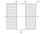
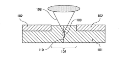
このレーザ加工方法について、図面に基づいて説明する。図9は被レーザ加工物である半導体基板の分割ラインおよびその周辺を示す平面図、図10はレーザ加工中の図9に示すC−C’断面図である。図9および図10において、101は半導体基板、102は半導体基板101に形成された半導体装置を構成する半導体デバイス(半導体素子)、104は半導体デバイス102の分割ライン、108はレーザ光、109は改質領域、110は改質領域109を起点として生じた切断部(クラック)を示している。
This laser processing method will be described with reference to the drawings. FIG. 9 is a plan view showing a parting line and its periphery of a semiconductor substrate that is a laser workpiece, and FIG. 10 is a cross-sectional view taken along the line C-C 'shown in FIG. 9 and 10,
以下、レーザ加工方法の工程を説明する。
まず、レーザ光108を半導体基板101の内部に集光点をあわせ、所定の厚み方向に多光子吸収を生じさせる。
Hereinafter, steps of the laser processing method will be described.
First, the
次に、多光子吸収を連続的、または断続的に生じさせながら、レーザ光108を分割ライン104の中心に沿って走査させることにより、半導体基板101の内部に、分割ライン104に沿った改質領域109を形成し、切断部110を形成する。
Next, the
次に、半導体基板101の両端に同時に外力をかけて、改質領域109を起点として半導体基板101を割り、半導体装置を形成する。このとき、改質領域109を起点として、切断部110が形成されているため、比較的小さな外力で、半導体基板101を容易に割ることができる。なお、特に半導体基板101が薄い場合は、特に外力を与えないでも、自然に厚み方向に割れる。
Next, an external force is applied to both ends of the
また上記レーザ加工による方法以外に、切削水圧力によりダイアフラム構造や梁構造が破壊されてしまうという課題を解決する他の方法として、分割ライン上に予め異方性エッチングなどで溝を形成しておき、加工部分の厚みを抑える方法がある。この方法は、例えば特許文献2に開示されている。
In addition to the above laser processing method, as another method for solving the problem that the diaphragm structure or the beam structure is destroyed by the cutting water pressure, grooves are formed in advance on the dividing line by anisotropic etching or the like. There is a method of reducing the thickness of the processed part. This method is disclosed in
特許文献2に開示されている製造方法では、まず方位面(100)面の半導体基板に、縦方向および横方向に分割ラインを開口するようにエッチング保護膜を形成し、その後、異方性エッチング処理を行う。このエッチング処理では、方位面(111)面でエッチングが止まるため、傾斜確度54.7度のV溝が形成される。次に、V溝が拡張するように半導体基板に外力を加えて、V溝に沿って半導体基板を分割し、個々の半導体装置を形成する。
しかしながら、特許文献1に開示されているレーザ加工方法では、半導体基板101が厚い場合においては、一回の走査による改質領域109では分割できないため、複数回レーザ加工を実施して、複数の改質領域109を厚み方向に平行に形成する必要があり、加工にかかるタクトの増加につながるという課題がある。
However, in the laser processing method disclosed in
また、特許文献2に開示されているV溝を形成する製造方法では、以下の課題がある。
分割ラインの縦方向および横方向にV溝が交差する部分においては、異方性エッチングの侵食が他の部分と異なるため、過剰にエッチングを行うと、方位面(111)面でエッチングが止まらず、例えば方位面(211)面にエッチングが進行する。すなわち、例えばV溝よりも深いエッチングを要するダイアフラム構造を形成する工程と同時にV溝を形成しようとした場合、V溝の交差部分が過剰にエッチングされ、半導体基板を貫通してしまうため、半導体基板の強度が極端に劣化し、ハンドリング時に半導体基板が破損してしまう。
Moreover, the manufacturing method for forming the V-groove disclosed in
At portions where the V-grooves intersect the vertical and horizontal directions of the dividing line, the erosion of anisotropic etching is different from other portions. Therefore, if etching is performed excessively, etching does not stop at the azimuth plane (111). For example, etching proceeds on the azimuth plane (211). That is, for example, when an attempt is made to form a V-groove simultaneously with the step of forming a diaphragm structure that requires etching deeper than the V-groove, the intersection of the V-groove is excessively etched and penetrates the semiconductor substrate. As a result, the strength of the semiconductor deteriorates extremely and the semiconductor substrate is damaged during handling.
そこで、本発明は、半導体基板の一部を薄厚化したダイアフラム構造や梁構造を有する半導体基板を個々の半導体装置に分割する際において、分割の品質を低下させることなく、加工タクトの向上を可能とする、すわなち、レーザ加工の走査回数を抑えることができ、且つ強度劣化による破損のない半導体装置の製造方法、およびこの製造方法により形成された半導体装置を実装する半導体モジュールの製造方法を提供することを目的とするものである。 Therefore, according to the present invention, when a semiconductor substrate having a diaphragm structure or a beam structure in which a part of the semiconductor substrate is thinned is divided into individual semiconductor devices, the processing tact can be improved without reducing the quality of the division. In other words, a method for manufacturing a semiconductor device that can suppress the number of scans of laser processing and that is not damaged by strength deterioration, and a method for manufacturing a semiconductor module that mounts a semiconductor device formed by this manufacturing method. It is intended to provide.
上記課題を解決するために、本発明のうち請求項1に記載の半導体装置の製造方法は、半導体基板に形成された、複数の半導体素子を個々に分割して半導体装置を製造する方法であって、前記複数の半導体素子を個々に分割するための、互いに交差する第一の方向および第二の方向の分割ラインを設定し、前記半導体素子を囲む、前記第一の方向および第二の方向の分割ラインのうち、第一の方向の分割ライン上にエッチングにより溝を形成する工程と、前記第一の方向の分割ラインに形成された前記溝のライン上、および第二の方向の分割ラインに沿って、レーザ光を照射して、半導体基板の内部に改質領域を形成する工程と、前記第一の方向および第二の方向の分割ラインに沿って半導体基板を分割して個々の半導体装置を形成する工程とを有し、前記溝は交差するパターンをもたないように形成されることを特徴とするものである。
In order to solve the above problems, a method for manufacturing a semiconductor device according to
また請求項2記載の半導体装置の製造方法は、請求項1に記載の半導体装置の製造方法であって、前記半導体素子に、ダイアフラム構造を形成する工程をさらに有することを特徴とする。
また請求項3記載の半導体装置の製造方法は、請求項1または請求項2に記載の半導体装置の製造方法であって、前記第一の方向の分割ライン上の溝は連続的に形成されることを特徴とする。
また請求項4記載の半導体装置の製造方法は、請求項1〜請求項3のいずれか1項に記載の半導体装置の製造方法であって、前記第一の方向の分割ラインに形成される溝は、V溝に形成されることを特徴とする。
また請求項5記載の半導体装置の製造方法は、請求項1〜請求項3のいずれか1項に記載の半導体装置の製造方法であって、前記第一の方向の分割ラインに形成される溝は、U溝に形成されることを特徴とする。
A method for manufacturing a semiconductor device according to
The method for manufacturing a semiconductor device according to
A method for manufacturing a semiconductor device according to
A method for manufacturing a semiconductor device according to
また請求項6に記載の半導体装置の製造方法は、請求項1〜請求項5のいずれか1項に記載の半導体装置の製造方法であって、前記第一の方向の分割ライン上に溝を形成する工程と、前記半導体装置にダイアフラム構造を形成する工程とが、異方性エッチングにより行われることを特徴とするものである。
また請求項7に記載の半導体装置の製造方法は、請求項1〜請求項6のいずれか1項に記載の半導体装置の製造方法であって、前記半導体基板の内部に改質領域を形成する工程において、前記溝が形成された第一の方向の分割ラインに沿ってレーザ光を走査する回数が、前記溝が形成されない第二の方向の分割ラインに沿ってレーザ光を走査する回数よりも少ないことを特徴とする。
また請求項8に記載の半導体装置の製造方法は、請求項1〜請求項7のいずれか1項に記載の半導体装置の製造方法であって、前記第一および第二の方向の分割ラインに沿って半導体基板を分割して個々の半導体装置を形成する工程は、前記半導体基板に外力を加えることにより行われることを特徴とする。
A method for manufacturing a semiconductor device according to a sixth aspect is the method for manufacturing a semiconductor device according to any one of the first to fifth aspects, wherein a groove is formed on the dividing line in the first direction. forming, and forming a diaphragm structure to the semiconductor device is characterized in dividing Rigyo by the anisotropic etching.
A method for manufacturing a semiconductor device according to
A method for manufacturing a semiconductor device according to claim 8 is the method for manufacturing a semiconductor device according to any one of
また請求項9に記載の半導体モジュールの製造方法は、前記請求項1〜請求項8のいずれかの半導体装置の製造方法において形成された半導体装置を、実装基板に固着する工程を有することを特徴とする。
また請求項10に記載の半導体モジュールの製造方法は、請求項9に記載の半導体モジュールの製造方法であって、前記半導体装置を実装基板に固着する工程において、前記半導体装置の裏面が、ダイボンド材によって前記実装基板の上面に接着されることを特徴とするものである。
The method for manufacturing a semiconductor module according to claim 9 includes a step of fixing the semiconductor device formed in the method for manufacturing a semiconductor device according to any one of
The method for manufacturing a semiconductor module according to
また請求項11に記載の半導体装置の製造方法は、半導体基板に形成された、複数の半導体素子を個々に分割して半導体装置を製造する方法であって、前記複数の半導体素子を個々に分割するための、互いに交差する第一の方向および第二の方向の分割ラインを設定し、前記半導体素子を囲む、前記第一の方向および第二の方向の分割ラインのうち、一方向の分割ライン上にエッチングにより溝を形成する工程と、前記第一の方向および第二の方向の分割ラインに沿って、レーザ光を照射して、半導体基板の内部に改質領域を形成する工程と、前記第一の方向および第二の方向の分割ラインに沿って半導体基板を分割して個々の半導体装置を形成する工程とを有し、前記溝は交差するパターンをもたないように形成され、前記半導体基板の内部に改質領域を形成する工程において、前記溝が形成された分割ラインに沿ってレーザ光を走査する回数が、前記溝が形成されない分割ラインに沿ってレーザ光を走査する回数よりも少ないことを特徴とするものである。
A method of manufacturing a semiconductor device according to
本発明の半導体装置の製造方法は、交差する第一の方向および第二の方向の分割ラインのうち第一の方向の分割ライン上のみに、溝をエッチングで形成するため、エッチングの制御が極めて難しい溝の交差部分ができないので、極めて容易に安定した溝を形成でき、また溝の形成された第一の方向の分割ラインに沿って個々の半導体装置に分割するため、溝を形成しない場合に比較して、容易に直進性に優れた分割を行うことができる、という効果を有している。 In the method of manufacturing a semiconductor device according to the present invention, the grooves are formed by etching only on the dividing lines in the first direction among the intersecting lines in the first direction and the second direction. Since there are no difficult groove intersections, stable grooves can be formed very easily, and the semiconductor device is divided along the dividing lines in the first direction where the grooves are formed. In comparison, it has an effect that it is possible to easily perform division with excellent straightness.
また本発明の半導体装置の製造方法は、半導体基板を個々の半導体装置に分割する工程において、半導体基板を個々の半導体装置に分割するための起点となる半導体基板内部に改質領域を形成する際、溝が形成された分割ラインに沿ってレーザ光を走査する回数が、溝が形成されない分割ラインに沿ってレーザ光を走査する回数よりも少なくても、直進性のよい安定した分割が可能であり、分割ラインに溝が形成されていない場合と比較して加工タクトを短縮することができる、という効果を有している。 The method of manufacturing a semiconductor device according to the present invention includes a step of dividing a semiconductor substrate into individual semiconductor devices when forming a modified region inside the semiconductor substrate that is a starting point for dividing the semiconductor substrate into individual semiconductor devices. Even if the number of times the laser beam is scanned along the dividing line in which the groove is formed is less than the number of times the laser beam is scanned along the dividing line in which the groove is not formed, stable division with good straightness is possible. There is an effect that the machining tact time can be shortened as compared with the case where no groove is formed in the dividing line.
以下、本発明の実施の形態を、図面を参照しながら説明する。
図1は、本発明の実施形態における複数の半導体素子が形成された半導体基板の平面図、図2は図1の拡大図、図3および図4はそれぞれ図2におけるA−A’断面図、B−B’断面図である。
Hereinafter, embodiments of the present invention will be described with reference to the drawings.
1 is a plan view of a semiconductor substrate on which a plurality of semiconductor elements according to an embodiment of the present invention are formed, FIG. 2 is an enlarged view of FIG. 1, and FIGS. 3 and 4 are cross-sectional views taken along line AA ′ in FIG. It is BB 'sectional drawing.
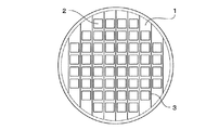
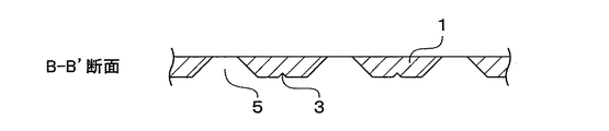
図1〜図4において、1はSi単結晶からなる半導体基板、2は半導体装置を構成する半導体デバイス(半導体素子)、3はV溝(溝の一例)、4は分割ライン、5はダイアフラムを示しており、図3のA−A’断面図は、横方向の分割ライン4に沿った半導体基板1の断面図、図4のB−B’断面図は、ダイアフラム5が形成された半導体デバイス2に沿った横方向の半導体基板1の断面図である。
1 to 4, 1 is a semiconductor substrate made of Si single crystal, 2 is a semiconductor device (semiconductor element) constituting a semiconductor device, 3 is a V groove (an example of a groove), 4 is a dividing line, and 5 is a diaphragm. 3 is a cross-sectional view of the
図1および図2に示すように、半導体基板1には、縦方向および横方向に桝目状に複数の半導体デバイス2が形成されており、半導体デバイス2には、それぞれダイアフラム5が形成されている。
As shown in FIGS. 1 and 2, a plurality of
また複数の半導体デバイス2は、分割ライン4で区切られている。ここで分割ライン4は、半導体基板1から、半導体デバイス2を個々に分割する際に設定される分割領域である。そして、分割ライン4は、縦方向および横方向に直交する(交差する)ように形成されており、これら直交する分割ラインのうち、縦方向または横方向の一方の平行する分割ライン(図では縦方向の分割ライン)上のみにV溝3が形成されている。これらV溝3は、例えば傾斜角度が54.7度となる方位面(111)面で形成されている。
Further, the plurality of
次に、図5を参照して、本発明の半導体装置の製造方法を説明する。図5は、図4に示すB−B’断面図を用いた本発明の半導体装置の製造方法の工程を順にを示す断面図である。図5において、6はエッチングマスク、7はエキスパンドテープ、8はレーザ光、9は改質領域、10は改質領域を起点としたクラック(切断部)、11は半導体基板1から個々の半導体デバイス2を切り出した後の半導体装置を示している。
Next, a method for manufacturing a semiconductor device of the present invention will be described with reference to FIG. FIG. 5 is a cross-sectional view sequentially illustrating the steps of the method for manufacturing a semiconductor device of the present invention using the B-B ′ cross-sectional view shown in FIG. 4. In FIG. 5, 6 is an etching mask, 7 is an expanded tape, 8 is a laser beam, 9 is a modified region, 10 is a crack (cut) from the modified region, and 11 is an individual semiconductor device from the
まず、「縦方向の平行する分割ライン上のみに連続して、異方性エッチングによりV溝を形成する工程」を実行する。
すなわち、まず図5(a)に示すように、複数の半導体デバイス2が形成され、個々の半導体デバイス2を分割するための分割ライン(図示せず)が設定された半導体基板1に、エッチングマスク6を形成する。エッチングマスク6は、ダイアフラム5およびV溝3を形成したい領域が開口するように形成する。このとき、V溝3を形成するためのエッチングマスク6の開口は、一方の平行する分割ライン4上のみに形成する。
First, the “step of forming V-grooves by anisotropic etching continuously only on vertical parallel dividing lines” is executed.
That is, first, as shown in FIG. 5A, an etching mask is formed on a
ここで、例えばエッチングマスク6は、シリコン酸化膜などの材料をCVD法を用いて形成した後、リソグラフィ技術でパターニングして形成する。なお、図示していないが、このとき半導体デバイス2が形成された面には全面にエッチングマスクを残しておく。
Here, for example, the etching mask 6 is formed by forming a material such as a silicon oxide film using a CVD method and then patterning the material using a lithography technique. Although not shown, an etching mask is left on the entire surface where the
次に、図5(b)に示すように、ダイアフラム5およびV溝3を異方性エッチングにより形成する。ここで、異方性エッチング液としては、例えばKOH溶液や、TMAH(水酸化テトラメチルアンモニウム)溶液が使用される。このとき、V溝3は一方の平行する分割ライン4上のみに形成されるので、交差するパターンをもたない。よって、Si単結晶基板からなる半導体基板1のエッチングは、交差パターン部分の異常侵食がなく、方位面(111)面で確実に進行が止まるため、エッチング深さの異なるダイアフラム5と、V溝3を同時に形成しても、傾斜角54.7度となる深さでストップさせることができる。つまりV溝3の深さと幅は、エッチングマスク6の開口幅で決定できる。
Next, as shown in FIG. 5B, the
次に図5(c)に示すように、エッチングマスク6を除去する。エッチングマスク6の除去には、例えばBHF溶液を用いる。ここで、エッチングマスク6を除去しているが、特に必要なければ、エッチングマスク6は残しておいても構わない。 Next, as shown in FIG. 5C, the etching mask 6 is removed. For example, a BHF solution is used to remove the etching mask 6. Here, the etching mask 6 is removed, but the etching mask 6 may be left if not particularly required.
続いて、「直交する分割ラインに沿ってそれぞれ、レーザ光を半導体基板の内部に焦点をあわせて照射して、半導体基板の内部に改質領域を形成する工程」を実行する。
すなわち、まず図5(d)に示すように、エキスパンドテープ7に半導体基板1をマウントする。
Subsequently, “a step of forming a modified region in the semiconductor substrate by irradiating the inside of the semiconductor substrate with a laser beam focused along each of the orthogonal dividing lines” is performed.
That is, first, as shown in FIG. 5D, the
次に、図5(e)に示すように、直交する分割ライン4に沿ってそれぞれ、レーザ光8を半導体基板1の内部に焦点をあわせて照射して、半導体基板1の内部に改質領域9を形成する。このとき、縦方向のレーザ光8の走査は、V溝3のライン上に沿って実施し、改質領域9から発生するマイクロクラックがV溝3に進展するように実施する。
Next, as shown in FIG. 5 (e), a laser beam 8 is focused on the inside of the
最後に、「半導体基板に外力を加えることにより、直交する分割ラインに沿って半導体基板を個々の半導体装置に分割する工程」を実行する。
すなわち、図5(f)に示すように、エキスパンドテープ7に外力を加えて、直交する分割ライン4に沿ってそれぞれ形成された改質領域9からクラック10を進展させて半導体基板1を分割し、個々の半導体装置11を形成する。
Finally, the “step of dividing the semiconductor substrate into individual semiconductor devices along the orthogonal dividing lines by applying an external force to the semiconductor substrate” is executed.
That is, as shown in FIG. 5 (f), an external force is applied to the expanded
ここで、半導体基板1が厚い場合、レーザ光8の走査を複数回行って改質領域9を複数形成することにより、分割を容易にすることができるが、図6(a),(b)に示すように、V溝3が形成されている分割ライン4に沿ってレーザ光8を走査する回数は、V溝3が形成されていない分割ライン4に沿ってレーザ光8を走査する回数より少なくても、分割が可能である。
Here, when the
図6(a)は、上記半導体基板1のB−B’断面の拡大図であり、V溝3が形成された分割ライン4に沿って形成された、レーザ光8の走査回数を2回としたときの深さ方向の改質領域9a,9bを示し、また図6(b)は、ダイアフラム5が形成された半導体デバイス2に沿った縦方向の半導体基板1のC−C’断面の拡大図であり、V溝3が形成されていない分割ライン4に沿って形成された、レーザ光8の走査回数を3回としたときの深さ方向の改質領域9a,9b,9cを示している。
FIG. 6A is an enlarged view of the BB ′ cross section of the
このようにして、個々に分割された半導体装置11は、図7に示すように、ダイアフラム構造を有する半導体装置となる。
以上のように、半導体基板1の構成および半導体装置11の製造方法によれば、半導体基板1を個々の半導体装置11に分割するための起点となる改質領域9を形成する際、V溝3が形成された分割ライン4に沿ってレーザ光8を走査する回数を、V溝3の無い分割ライン4に沿ってレーザ光8を走査する回数よりも少なくすることができ、加工タクトを短くすることができ、また直進性の良い安定した分割を可能にできる。
In this way, the individually divided
As described above, according to the configuration of the
また直交する分割ライン4のうち一方の平行する分割ライン上のみに、V溝3を連続するようにエッチングで形成するため、エッチングの制御が極めて難しいV溝3の交差部分ができないことにより、極めて容易に安定したV溝3を形成でき、また連続したV溝3が形成された分割ライン4に沿って個々の半導体装置11に分割するため、V溝3を形成しない場合と比較して、容易に直進性に優れた分割を行うことができる。
Further, since the V-
またV溝3の形成は、ダイアフラム構造を形成する異方性エッチング工程と同時に行われるため、特に工程の増加がなく、コストアップや、リードタイムが増加することを回避できる。
Further, since the V-
図7に、分割された後の半導体装置の平面図、横断面図、縦断面図を示す。図7において、11は個々に分割された後の半導体装置、12はV溝の頂点を起点に分割された際にできる面取りであり、個々の半導体装置11の裏面側において対向する2辺のみに、面取り12が形成されている。
FIG. 7 shows a plan view, a transverse sectional view, and a longitudinal sectional view of the semiconductor device after being divided. In FIG. 7,
図7に示すように、V溝3が形成された部分に相当する面取り12の部分は、半導体装置11の長辺側に配置している。すなわち、V溝3を形成する分割ライン4として、半導体装置11の長辺側に沿った分割ラインを選択し、V溝3を形成している。
As shown in FIG. 7, the chamfered
一般的に半導体装置は長細いと折れやすいが、折れる際の起点は、長辺側にできたクラックであり、長辺側を面取りすることで、起点となるクラックが無くなるため半導体装置の抗折強度は、飛躍的に向上する。すなわち、半導体装置11の抗折強度の低下につながる長辺のチッピングが抑制され、機械的強度の優れた半導体装置11を得ることができる。
Generally, a semiconductor device is easy to bend when it is long and thin, but the starting point when bending is a crack formed on the long side, and chamfering the long side eliminates the crack that becomes the starting point. The strength is dramatically improved. That is, long-side chipping that leads to a decrease in the bending strength of the
図8に本発明の半導体装置が基板に実装されている状態の断面図を示す。図8において、13は実装基板、14は実装基板13と半導体装置11を接着するためのダイボンド材である。
FIG. 8 shows a cross-sectional view of the semiconductor device of the present invention mounted on a substrate. In FIG. 8,
通常、半導体装置11と実装基板13との接着はダイボンド材14で行われるが、接着の際には半導体装置11の側面への這い上がりを制御するために、ダイボンド材14の塗布量を厳しく制御する必要がある。図8に示すように、半導体装置11に面取り12が施されている場合、ダイボンド材の半導体装置11の側面への這い上がりは、面取り12の表面張力によって抑制されるため、従来よりも極めて容易に管理が可能である。また残りの二辺側(短辺側)には面取りを行わないことで、短辺側の半導体装置11の裏面の面積を減少させることがなく、ダイボンド時の接着面積を確保できる。
Usually, the bonding between the
なお、本実施の形態では、半導体基板1および半導体装置11にダイアフラム構造を形成しているが、特にダイアフラム構造でなくても勿論構わない。
また本実施の形態では、直交する分割ラインのうち、縦方向または横方向の一方の平行する分割ライン上のみに形成されている溝を、V溝としているが、V溝に限ることはなく、U溝とすることも可能である。また溝を異方性エッチングにより形成しているが、ドライエッチングにより形成することも可能である。
In the present embodiment, the diaphragm structure is formed in the
In the present embodiment, the grooves formed only on one of the vertical or horizontal parallel dividing lines among the orthogonal dividing lines are V-grooves, but are not limited to V-grooves. A U-groove is also possible. The grooves are formed by anisotropic etching, but can be formed by dry etching.
本発明の半導体基板、および半導体装置ならびにその半導体装置の製造方法は、シリコン基板や、化合物半導体基板の分割において、加工コストの増加や、加工の品質を低下させることなく、半導体装置を製造するのに適し、特にダイアフラム構造を有するMEMSセンサ等を製造する際の分割として有用である。 The semiconductor substrate, the semiconductor device, and the method for manufacturing the semiconductor device according to the present invention can manufacture a semiconductor device without increasing processing costs or reducing processing quality in dividing a silicon substrate or a compound semiconductor substrate. In particular, it is useful as a division when manufacturing a MEMS sensor or the like having a diaphragm structure.
1 半導体基板
2 半導体デバイス
3 V溝
4 分割ライン
5 ダイアフラム
6 エッチングマスク
7 エキスパンドテープ
8 レーザ光
9,9a,9b,9c 改質領域
10 クラック
11 半導体装置
12 面取り
13 実装基板
14 ダイボンド材
DESCRIPTION OF
Claims (11)
前記複数の半導体素子を個々に分割するための、互いに交差する第一の方向および第二の方向の分割ラインを設定し、前記半導体素子を囲む、前記第一の方向および第二の方向の分割ラインのうち、第一の方向の分割ライン上にエッチングにより溝を形成する工程と、
前記第一の方向の分割ラインに形成された前記溝のライン上、および第二の方向の分割ラインに沿って、レーザ光を照射して、半導体基板の内部に改質領域を形成する工程と、
前記第一の方向および第二の方向の分割ラインに沿って半導体基板を分割して個々の半導体装置を形成する工程と
を有し、
前記溝は交差するパターンをもたないように形成されること
を特徴とする半導体装置の製造方法。 A method of manufacturing a semiconductor device by individually dividing a plurality of semiconductor elements formed on a semiconductor substrate,
A division line in the first direction and the second direction for setting the division lines in the first direction and the second direction intersecting each other to divide the plurality of semiconductor elements individually, and surrounding the semiconductor element. Forming a groove by etching on the dividing line in the first direction among the lines;
Irradiating a laser beam on the groove line formed in the dividing line in the first direction and along the dividing line in the second direction to form a modified region inside the semiconductor substrate; ,
Dividing the semiconductor substrate along division lines in the first direction and the second direction to form individual semiconductor devices,
The method of manufacturing a semiconductor device, wherein the grooves are formed so as not to have an intersecting pattern.
を特徴とする請求項1記載の半導体装置の製造方法。 2. The method of manufacturing a semiconductor device according to claim 1, further comprising a step of forming a diaphragm structure in the semiconductor element.
を特徴とする請求項1または請求項2に記載の半導体装置の製造方法。 The method for manufacturing a semiconductor device according to claim 1, wherein the grooves on the dividing lines in the first direction are formed continuously.
を特徴とする請求項1〜請求項3のいずれか1項に記載の半導体装置の製造方法。 4. The method of manufacturing a semiconductor device according to claim 1, wherein the groove formed in the dividing line in the first direction is formed in a V-groove. 5.
を特徴とする請求項1〜請求項3のいずれか1項に記載の半導体装置の製造方法。 4. The method of manufacturing a semiconductor device according to claim 1, wherein the groove formed in the dividing line in the first direction is formed in a U-groove. 5.
を特徴とする請求項1〜請求項5のいずれか1項に記載の半導体装置の製造方法。 Forming a groove in the first direction of the division on the line, and forming a diaphragm structure to the semiconductor device, according to claim 1 claims, characterized in that dividing Rigyo by the anisotropic etching 6. A method of manufacturing a semiconductor device according to any one of 5 above.
前記溝が形成された第一の方向の分割ラインに沿ってレーザ光を走査する回数が、前記溝が形成されない第二の方向の分割ラインに沿ってレーザ光を走査する回数よりも少ないこと
を特徴とする請求項1〜請求項6のいずれか1項に記載の半導体装置の製造方法。 In the step of forming a modified region inside the semiconductor substrate,
The number of times the laser beam is scanned along the dividing line in the first direction where the groove is formed is less than the number of times the laser beam is scanned along the dividing line in the second direction where the groove is not formed. The method for manufacturing a semiconductor device according to claim 1, wherein the method is a semiconductor device manufacturing method.
を特徴とする請求項1〜請求項7のいずれか1項に記載の半導体装置の製造方法。 The step of dividing the semiconductor substrate along the dividing lines in the first and second directions to form individual semiconductor devices is performed by applying an external force to the semiconductor substrate. The method for manufacturing a semiconductor device according to claim 7.
を特徴とする半導体モジュールの製造方法。 A method for manufacturing a semiconductor module, comprising a step of fixing the semiconductor device formed in the method for manufacturing a semiconductor device according to any one of claims 1 to 8 to a mounting substrate.
を特徴とする請求項9記載の半導体モジュールの製造方法。 The method for manufacturing a semiconductor module according to claim 9, wherein, in the step of fixing the semiconductor device to the mounting substrate, the back surface of the semiconductor device is bonded to the upper surface of the mounting substrate by a die bonding material.
前記複数の半導体素子を個々に分割するための、互いに交差する第一の方向および第二の方向の分割ラインを設定し、前記半導体素子を囲む、前記第一の方向および第二の方向の分割ラインのうち、一方向の分割ライン上にエッチングにより溝を形成する工程と、A division line in the first direction and the second direction for setting the division lines in the first direction and the second direction intersecting each other to divide the plurality of semiconductor elements individually, and surrounding the semiconductor element. Forming a groove by etching on a dividing line in one direction among the lines;
前記第一の方向および第二の方向の分割ラインに沿って、レーザ光を照射して、半導体基板の内部に改質領域を形成する工程と、Irradiating laser light along the first and second dividing lines to form a modified region inside the semiconductor substrate;
前記第一の方向および第二の方向の分割ラインに沿って半導体基板を分割して個々の半導体装置を形成する工程とDividing the semiconductor substrate along the dividing lines in the first direction and the second direction to form individual semiconductor devices;
を有し、Have
前記溝は交差するパターンをもたないように形成され、The grooves are formed so as not to have an intersecting pattern,
前記半導体基板の内部に改質領域を形成する工程において、前記溝が形成された分割ラインに沿ってレーザ光を走査する回数が、前記溝が形成されない分割ラインに沿ってレーザ光を走査する回数よりも少ないことIn the step of forming the modified region inside the semiconductor substrate, the number of times the laser beam is scanned along the dividing line where the groove is formed is the number of times the laser beam is scanned along the dividing line where the groove is not formed. Less than
を特徴とする半導体装置の製造方法。A method of manufacturing a semiconductor device.
Priority Applications (4)
| Application Number | Priority Date | Filing Date | Title |
|---|---|---|---|
| JP2006133160A JP4372115B2 (en) | 2006-05-12 | 2006-05-12 | Semiconductor device manufacturing method and semiconductor module manufacturing method |
| CNA2007101013117A CN101071790A (en) | 2006-05-12 | 2007-04-16 | Semiconductor substrate, and semiconductor device and method of manufacturing the semiconductor device |
| US11/797,292 US7808059B2 (en) | 2006-05-12 | 2007-05-02 | Semiconductor substrate, and semiconductor device and method of manufacturing the semiconductor device |
| US12/570,548 US7754584B2 (en) | 2006-05-12 | 2009-09-30 | Semiconductor substrate, and semiconductor device and method of manufacturing the semiconductor device |
Applications Claiming Priority (1)
| Application Number | Priority Date | Filing Date | Title |
|---|---|---|---|
| JP2006133160A JP4372115B2 (en) | 2006-05-12 | 2006-05-12 | Semiconductor device manufacturing method and semiconductor module manufacturing method |
Related Child Applications (1)
| Application Number | Title | Priority Date | Filing Date |
|---|---|---|---|
| JP2009124791A Division JP2009188428A (en) | 2009-05-25 | 2009-05-25 | Semiconductor substrate |
Publications (3)
| Publication Number | Publication Date |
|---|---|
| JP2007305810A JP2007305810A (en) | 2007-11-22 |
| JP2007305810A5 JP2007305810A5 (en) | 2009-07-02 |
| JP4372115B2 true JP4372115B2 (en) | 2009-11-25 |
Family
ID=38685663
Family Applications (1)
| Application Number | Title | Priority Date | Filing Date |
|---|---|---|---|
| JP2006133160A Active JP4372115B2 (en) | 2006-05-12 | 2006-05-12 | Semiconductor device manufacturing method and semiconductor module manufacturing method |
Country Status (3)
| Country | Link |
|---|---|
| US (2) | US7808059B2 (en) |
| JP (1) | JP4372115B2 (en) |
| CN (1) | CN101071790A (en) |
Families Citing this family (105)
| Publication number | Priority date | Publication date | Assignee | Title |
|---|---|---|---|---|
| US7859084B2 (en) * | 2008-02-28 | 2010-12-28 | Panasonic Corporation | Semiconductor substrate |
| JP2009206292A (en) * | 2008-02-28 | 2009-09-10 | Panasonic Corp | Semiconductor substrate, and manufacturing method of semiconductor device |
| JP2009206291A (en) * | 2008-02-28 | 2009-09-10 | Panasonic Corp | Semiconductor substrate, semiconductor device, and manufacturing method thereof |
| US8872287B2 (en) | 2008-03-27 | 2014-10-28 | United Microelectronics Corp. | Integrated structure for MEMS device and semiconductor device and method of fabricating the same |
| JP5399794B2 (en) * | 2009-07-07 | 2014-01-29 | 日本特殊陶業株式会社 | Manufacturing method of ceramic heater |
| US8642448B2 (en) | 2010-06-22 | 2014-02-04 | Applied Materials, Inc. | Wafer dicing using femtosecond-based laser and plasma etch |
| JP2012089709A (en) * | 2010-10-20 | 2012-05-10 | Disco Abrasive Syst Ltd | Method for dividing workpiece |
| JP5659689B2 (en) * | 2010-10-21 | 2015-01-28 | 富士電機株式会社 | Manufacturing method of reverse blocking IGBT |
| US8666530B2 (en) * | 2010-12-16 | 2014-03-04 | Electro Scientific Industries, Inc. | Silicon etching control method and system |
| US8557683B2 (en) | 2011-06-15 | 2013-10-15 | Applied Materials, Inc. | Multi-step and asymmetrically shaped laser beam scribing |
| US8912077B2 (en) | 2011-06-15 | 2014-12-16 | Applied Materials, Inc. | Hybrid laser and plasma etch wafer dicing using substrate carrier |
| US8598016B2 (en) | 2011-06-15 | 2013-12-03 | Applied Materials, Inc. | In-situ deposited mask layer for device singulation by laser scribing and plasma etch |
| US9126285B2 (en) | 2011-06-15 | 2015-09-08 | Applied Materials, Inc. | Laser and plasma etch wafer dicing using physically-removable mask |
| US8703581B2 (en) | 2011-06-15 | 2014-04-22 | Applied Materials, Inc. | Water soluble mask for substrate dicing by laser and plasma etch |
| US8759197B2 (en) | 2011-06-15 | 2014-06-24 | Applied Materials, Inc. | Multi-step and asymmetrically shaped laser beam scribing |
| US8507363B2 (en) | 2011-06-15 | 2013-08-13 | Applied Materials, Inc. | Laser and plasma etch wafer dicing using water-soluble die attach film |
| US9129904B2 (en) | 2011-06-15 | 2015-09-08 | Applied Materials, Inc. | Wafer dicing using pulse train laser with multiple-pulse bursts and plasma etch |
| US8557682B2 (en) | 2011-06-15 | 2013-10-15 | Applied Materials, Inc. | Multi-layer mask for substrate dicing by laser and plasma etch |
| US9029242B2 (en) | 2011-06-15 | 2015-05-12 | Applied Materials, Inc. | Damage isolation by shaped beam delivery in laser scribing process |
| US8951819B2 (en) | 2011-07-11 | 2015-02-10 | Applied Materials, Inc. | Wafer dicing using hybrid split-beam laser scribing process with plasma etch |
| JP5939752B2 (en) * | 2011-09-01 | 2016-06-22 | 株式会社ディスコ | Wafer dividing method |
| US8652940B2 (en) | 2012-04-10 | 2014-02-18 | Applied Materials, Inc. | Wafer dicing used hybrid multi-step laser scribing process with plasma etch |
| US8946057B2 (en) | 2012-04-24 | 2015-02-03 | Applied Materials, Inc. | Laser and plasma etch wafer dicing using UV-curable adhesive film |
| US8969177B2 (en) | 2012-06-29 | 2015-03-03 | Applied Materials, Inc. | Laser and plasma etch wafer dicing with a double sided UV-curable adhesive film |
| US9048309B2 (en) | 2012-07-10 | 2015-06-02 | Applied Materials, Inc. | Uniform masking for wafer dicing using laser and plasma etch |
| US8993414B2 (en) | 2012-07-13 | 2015-03-31 | Applied Materials, Inc. | Laser scribing and plasma etch for high die break strength and clean sidewall |
| US8859397B2 (en) | 2012-07-13 | 2014-10-14 | Applied Materials, Inc. | Method of coating water soluble mask for laser scribing and plasma etch |
| US8940619B2 (en) | 2012-07-13 | 2015-01-27 | Applied Materials, Inc. | Method of diced wafer transportation |
| US8845854B2 (en) | 2012-07-13 | 2014-09-30 | Applied Materials, Inc. | Laser, plasma etch, and backside grind process for wafer dicing |
| US9159574B2 (en) | 2012-08-27 | 2015-10-13 | Applied Materials, Inc. | Method of silicon etch for trench sidewall smoothing |
| US9252057B2 (en) | 2012-10-17 | 2016-02-02 | Applied Materials, Inc. | Laser and plasma etch wafer dicing with partial pre-curing of UV release dicing tape for film frame wafer application |
| US20140145294A1 (en) * | 2012-11-28 | 2014-05-29 | Nxp B.V. | Wafer separation |
| US8975162B2 (en) | 2012-12-20 | 2015-03-10 | Applied Materials, Inc. | Wafer dicing from wafer backside |
| US9236305B2 (en) | 2013-01-25 | 2016-01-12 | Applied Materials, Inc. | Wafer dicing with etch chamber shield ring for film frame wafer applications |
| US8980726B2 (en) | 2013-01-25 | 2015-03-17 | Applied Materials, Inc. | Substrate dicing by laser ablation and plasma etch damage removal for ultra-thin wafers |
| WO2014159464A1 (en) | 2013-03-14 | 2014-10-02 | Applied Materials, Inc. | Multi-layer mask including non-photodefinable laser energy absorbing layer for substrate dicing by laser and plasma etch |
| EP2801830B1 (en) * | 2013-05-08 | 2016-11-30 | NanoWorld AG | Wafer with probes for a scanning force microscope |
| US8883614B1 (en) | 2013-05-22 | 2014-11-11 | Applied Materials, Inc. | Wafer dicing with wide kerf by laser scribing and plasma etching hybrid approach |
| US9105710B2 (en) | 2013-08-30 | 2015-08-11 | Applied Materials, Inc. | Wafer dicing method for improving die packaging quality |
| US9224650B2 (en) | 2013-09-19 | 2015-12-29 | Applied Materials, Inc. | Wafer dicing from wafer backside and front side |
| US9460966B2 (en) | 2013-10-10 | 2016-10-04 | Applied Materials, Inc. | Method and apparatus for dicing wafers having thick passivation polymer layer |
| US9041198B2 (en) | 2013-10-22 | 2015-05-26 | Applied Materials, Inc. | Maskless hybrid laser scribing and plasma etching wafer dicing process |
| US9312177B2 (en) | 2013-12-06 | 2016-04-12 | Applied Materials, Inc. | Screen print mask for laser scribe and plasma etch wafer dicing process |
| US9299614B2 (en) | 2013-12-10 | 2016-03-29 | Applied Materials, Inc. | Method and carrier for dicing a wafer |
| US9293304B2 (en) | 2013-12-17 | 2016-03-22 | Applied Materials, Inc. | Plasma thermal shield for heat dissipation in plasma chamber |
| US9018079B1 (en) | 2014-01-29 | 2015-04-28 | Applied Materials, Inc. | Wafer dicing using hybrid laser scribing and plasma etch approach with intermediate reactive post mask-opening clean |
| US9012305B1 (en) | 2014-01-29 | 2015-04-21 | Applied Materials, Inc. | Wafer dicing using hybrid laser scribing and plasma etch approach with intermediate non-reactive post mask-opening clean |
| US9299611B2 (en) | 2014-01-29 | 2016-03-29 | Applied Materials, Inc. | Method of wafer dicing using hybrid laser scribing and plasma etch approach with mask plasma treatment for improved mask etch resistance |
| US8927393B1 (en) | 2014-01-29 | 2015-01-06 | Applied Materials, Inc. | Water soluble mask formation by dry film vacuum lamination for laser and plasma dicing |
| US9236284B2 (en) | 2014-01-31 | 2016-01-12 | Applied Materials, Inc. | Cooled tape frame lift and low contact shadow ring for plasma heat isolation |
| US8991329B1 (en) | 2014-01-31 | 2015-03-31 | Applied Materials, Inc. | Wafer coating |
| US9130030B1 (en) | 2014-03-07 | 2015-09-08 | Applied Materials, Inc. | Baking tool for improved wafer coating process |
| US20150255349A1 (en) | 2014-03-07 | 2015-09-10 | JAMES Matthew HOLDEN | Approaches for cleaning a wafer during hybrid laser scribing and plasma etching wafer dicing processes |
| US9275902B2 (en) | 2014-03-26 | 2016-03-01 | Applied Materials, Inc. | Dicing processes for thin wafers with bumps on wafer backside |
| US9076860B1 (en) | 2014-04-04 | 2015-07-07 | Applied Materials, Inc. | Residue removal from singulated die sidewall |
| US8975163B1 (en) | 2014-04-10 | 2015-03-10 | Applied Materials, Inc. | Laser-dominated laser scribing and plasma etch hybrid wafer dicing |
| US8932939B1 (en) | 2014-04-14 | 2015-01-13 | Applied Materials, Inc. | Water soluble mask formation by dry film lamination |
| US8912078B1 (en) | 2014-04-16 | 2014-12-16 | Applied Materials, Inc. | Dicing wafers having solder bumps on wafer backside |
| US8999816B1 (en) | 2014-04-18 | 2015-04-07 | Applied Materials, Inc. | Pre-patterned dry laminate mask for wafer dicing processes |
| US9159621B1 (en) | 2014-04-29 | 2015-10-13 | Applied Materials, Inc. | Dicing tape protection for wafer dicing using laser scribe process |
| US8912075B1 (en) | 2014-04-29 | 2014-12-16 | Applied Materials, Inc. | Wafer edge warp supression for thin wafer supported by tape frame |
| US8980727B1 (en) | 2014-05-07 | 2015-03-17 | Applied Materials, Inc. | Substrate patterning using hybrid laser scribing and plasma etching processing schemes |
| US9112050B1 (en) | 2014-05-13 | 2015-08-18 | Applied Materials, Inc. | Dicing tape thermal management by wafer frame support ring cooling during plasma dicing |
| US9034771B1 (en) | 2014-05-23 | 2015-05-19 | Applied Materials, Inc. | Cooling pedestal for dicing tape thermal management during plasma dicing |
| US9130057B1 (en) | 2014-06-30 | 2015-09-08 | Applied Materials, Inc. | Hybrid dicing process using a blade and laser |
| US9093518B1 (en) | 2014-06-30 | 2015-07-28 | Applied Materials, Inc. | Singulation of wafers having wafer-level underfill |
| US9165832B1 (en) | 2014-06-30 | 2015-10-20 | Applied Materials, Inc. | Method of die singulation using laser ablation and induction of internal defects with a laser |
| US9142459B1 (en) | 2014-06-30 | 2015-09-22 | Applied Materials, Inc. | Wafer dicing using hybrid laser scribing and plasma etch approach with mask application by vacuum lamination |
| US9349648B2 (en) | 2014-07-22 | 2016-05-24 | Applied Materials, Inc. | Hybrid wafer dicing approach using a rectangular shaped two-dimensional top hat laser beam profile or a linear shaped one-dimensional top hat laser beam profile laser scribing process and plasma etch process |
| US9117868B1 (en) | 2014-08-12 | 2015-08-25 | Applied Materials, Inc. | Bipolar electrostatic chuck for dicing tape thermal management during plasma dicing |
| US9196498B1 (en) | 2014-08-12 | 2015-11-24 | Applied Materials, Inc. | Stationary actively-cooled shadow ring for heat dissipation in plasma chamber |
| US9281244B1 (en) | 2014-09-18 | 2016-03-08 | Applied Materials, Inc. | Hybrid wafer dicing approach using an adaptive optics-controlled laser scribing process and plasma etch process |
| US11195756B2 (en) | 2014-09-19 | 2021-12-07 | Applied Materials, Inc. | Proximity contact cover ring for plasma dicing |
| US9177861B1 (en) | 2014-09-19 | 2015-11-03 | Applied Materials, Inc. | Hybrid wafer dicing approach using laser scribing process based on an elliptical laser beam profile or a spatio-temporal controlled laser beam profile |
| US9196536B1 (en) | 2014-09-25 | 2015-11-24 | Applied Materials, Inc. | Hybrid wafer dicing approach using a phase modulated laser beam profile laser scribing process and plasma etch process |
| US9130056B1 (en) | 2014-10-03 | 2015-09-08 | Applied Materials, Inc. | Bi-layer wafer-level underfill mask for wafer dicing and approaches for performing wafer dicing |
| US9245803B1 (en) | 2014-10-17 | 2016-01-26 | Applied Materials, Inc. | Hybrid wafer dicing approach using a bessel beam shaper laser scribing process and plasma etch process |
| US10692765B2 (en) | 2014-11-07 | 2020-06-23 | Applied Materials, Inc. | Transfer arm for film frame substrate handling during plasma singulation of wafers |
| US9330977B1 (en) | 2015-01-05 | 2016-05-03 | Applied Materials, Inc. | Hybrid wafer dicing approach using a galvo scanner and linear stage hybrid motion laser scribing process and plasma etch process |
| US9355907B1 (en) | 2015-01-05 | 2016-05-31 | Applied Materials, Inc. | Hybrid wafer dicing approach using a line shaped laser beam profile laser scribing process and plasma etch process |
| US9159624B1 (en) | 2015-01-05 | 2015-10-13 | Applied Materials, Inc. | Vacuum lamination of polymeric dry films for wafer dicing using hybrid laser scribing and plasma etch approach |
| TW201705528A (en) * | 2015-03-19 | 2017-02-01 | 晶元光電股份有限公司 | Light emitting device and method of fabricating the same |
| US9601375B2 (en) | 2015-04-27 | 2017-03-21 | Applied Materials, Inc. | UV-cure pre-treatment of carrier film for wafer dicing using hybrid laser scribing and plasma etch approach |
| US9478455B1 (en) | 2015-06-12 | 2016-10-25 | Applied Materials, Inc. | Thermal pyrolytic graphite shadow ring assembly for heat dissipation in plasma chamber |
| US9721839B2 (en) | 2015-06-12 | 2017-08-01 | Applied Materials, Inc. | Etch-resistant water soluble mask for hybrid wafer dicing using laser scribing and plasma etch |
| WO2017082210A1 (en) * | 2015-11-09 | 2017-05-18 | 古河電気工業株式会社 | Method for manufacturing semiconductor chip, and mask-integrated surface protection tape used therein |
| US9972575B2 (en) | 2016-03-03 | 2018-05-15 | Applied Materials, Inc. | Hybrid wafer dicing approach using a split beam laser scribing process and plasma etch process |
| JP2017162856A (en) * | 2016-03-07 | 2017-09-14 | 株式会社ディスコ | Processing method of wafer |
| US9852997B2 (en) | 2016-03-25 | 2017-12-26 | Applied Materials, Inc. | Hybrid wafer dicing approach using a rotating beam laser scribing process and plasma etch process |
| US9793132B1 (en) | 2016-05-13 | 2017-10-17 | Applied Materials, Inc. | Etch mask for hybrid laser scribing and plasma etch wafer singulation process |
| CN105880844A (en) * | 2016-05-23 | 2016-08-24 | 深圳市大德激光技术有限公司 | Laser cutting method capable of solving anisotropism |
| US10256149B2 (en) * | 2017-02-28 | 2019-04-09 | Infineon Technologies Austria Ag | Semiconductor wafer dicing crack prevention using chip peripheral trenches |
| US11158540B2 (en) | 2017-05-26 | 2021-10-26 | Applied Materials, Inc. | Light-absorbing mask for hybrid laser scribing and plasma etch wafer singulation process |
| US10363629B2 (en) | 2017-06-01 | 2019-07-30 | Applied Materials, Inc. | Mitigation of particle contamination for wafer dicing processes |
| CN109205552A (en) * | 2017-07-07 | 2019-01-15 | 中国科学院过程工程研究所 | A method of back corrosion cutting MEMS silicon wafer |
| US10535561B2 (en) | 2018-03-12 | 2020-01-14 | Applied Materials, Inc. | Hybrid wafer dicing approach using a multiple pass laser scribing process and plasma etch process |
| JP7093210B2 (en) * | 2018-03-28 | 2022-06-29 | 株式会社ディスコ | How to process plate-shaped objects |
| US11355394B2 (en) | 2018-09-13 | 2022-06-07 | Applied Materials, Inc. | Wafer dicing using hybrid laser scribing and plasma etch approach with intermediate breakthrough treatment |
| CN112090603B (en) * | 2019-06-17 | 2022-11-08 | 苏州天健云康信息科技有限公司 | Microfluidic device and method for manufacturing the same |
| CN112222630A (en) * | 2019-06-26 | 2021-01-15 | 大族激光科技产业集团股份有限公司 | Laser processing method |
| US11011424B2 (en) | 2019-08-06 | 2021-05-18 | Applied Materials, Inc. | Hybrid wafer dicing approach using a spatially multi-focused laser beam laser scribing process and plasma etch process |
| US11342226B2 (en) | 2019-08-13 | 2022-05-24 | Applied Materials, Inc. | Hybrid wafer dicing approach using an actively-focused laser beam laser scribing process and plasma etch process |
| US10903121B1 (en) | 2019-08-14 | 2021-01-26 | Applied Materials, Inc. | Hybrid wafer dicing approach using a uniform rotating beam laser scribing process and plasma etch process |
| US11600492B2 (en) | 2019-12-10 | 2023-03-07 | Applied Materials, Inc. | Electrostatic chuck with reduced current leakage for hybrid laser scribing and plasma etch wafer singulation process |
| US11211247B2 (en) | 2020-01-30 | 2021-12-28 | Applied Materials, Inc. | Water soluble organic-inorganic hybrid mask formulations and their applications |
Family Cites Families (15)
| Publication number | Priority date | Publication date | Assignee | Title |
|---|---|---|---|---|
| JPH04276645A (en) * | 1991-03-04 | 1992-10-01 | Toshiba Corp | Dicing method of compound semiconductor wafer |
| JPH05285935A (en) | 1992-04-13 | 1993-11-02 | Sumitomo Electric Ind Ltd | Dividing method for semiconductor base |
| JPH09320996A (en) * | 1996-03-29 | 1997-12-12 | Denso Corp | Manufacturing method for semiconductor device |
| US6271102B1 (en) * | 1998-02-27 | 2001-08-07 | International Business Machines Corporation | Method and system for dicing wafers, and semiconductor structures incorporating the products thereof |
| US6420245B1 (en) * | 1999-06-08 | 2002-07-16 | Kulicke & Soffa Investments, Inc. | Method for singulating semiconductor wafers |
| JP2001127008A (en) | 1999-10-22 | 2001-05-11 | Seiko Epson Corp | Method for dividing wafer and manufacturing method of semiconductor chip |
| JP3408805B2 (en) | 2000-09-13 | 2003-05-19 | 浜松ホトニクス株式会社 | Cutting origin region forming method and workpiece cutting method |
| US6420776B1 (en) * | 2001-03-01 | 2002-07-16 | Amkor Technology, Inc. | Structure including electronic components singulated using laser cutting |
| JP4288573B2 (en) | 2003-06-09 | 2009-07-01 | 富士電機ホールディングス株式会社 | Semiconductor wafer chip forming method |
| US6949449B2 (en) * | 2003-07-11 | 2005-09-27 | Electro Scientific Industries, Inc. | Method of forming a scribe line on a ceramic substrate |
| JP2005116844A (en) | 2003-10-09 | 2005-04-28 | Matsushita Electric Ind Co Ltd | Method for manufacturing semiconductor device |
| JP2005268752A (en) | 2004-02-19 | 2005-09-29 | Canon Inc | Method of laser cutting, workpiece and semiconductor-element chip |
| US7129114B2 (en) * | 2004-03-10 | 2006-10-31 | Micron Technology, Inc. | Methods relating to singulating semiconductor wafers and wafer scale assemblies |
| JP2006173428A (en) * | 2004-12-17 | 2006-06-29 | Seiko Epson Corp | Substrate machining method, and element manufacturing method |
| US7265034B2 (en) * | 2005-02-18 | 2007-09-04 | Taiwan Semiconductor Manufacturing Company, Ltd. | Method of cutting integrated circuit chips from wafer by ablating with laser and cutting with saw blade |
-
2006
- 2006-05-12 JP JP2006133160A patent/JP4372115B2/en active Active
-
2007
- 2007-04-16 CN CNA2007101013117A patent/CN101071790A/en active Pending
- 2007-05-02 US US11/797,292 patent/US7808059B2/en active Active
-
2009
- 2009-09-30 US US12/570,548 patent/US7754584B2/en active Active
Also Published As
| Publication number | Publication date |
|---|---|
| US7754584B2 (en) | 2010-07-13 |
| US20100015781A1 (en) | 2010-01-21 |
| US7808059B2 (en) | 2010-10-05 |
| JP2007305810A (en) | 2007-11-22 |
| CN101071790A (en) | 2007-11-14 |
| US20070264803A1 (en) | 2007-11-15 |
Similar Documents
| Publication | Publication Date | Title |
|---|---|---|
| JP4372115B2 (en) | Semiconductor device manufacturing method and semiconductor module manufacturing method | |
| US7859084B2 (en) | Semiconductor substrate | |
| KR100858983B1 (en) | Semiconductor device and dicing method for semiconductor substrate | |
| KR100791528B1 (en) | Method of machining substrate and method of manufacturing element | |
| CN102157447B (en) | Method for dicing a semiconductor wafer, a chip diced from a semiconductor wafer, and an array of chips diced from a semiconductor wafer | |
| JP2006286727A (en) | Semiconductor wafer provided with plurality of semiconductor devices and its dicing method | |
| JP2010003817A (en) | Laser dicing method, and laser dicing device | |
| JP2009124077A (en) | Semiconductor chip and its production process | |
| JP2009206291A (en) | Semiconductor substrate, semiconductor device, and manufacturing method thereof | |
| JP2007235008A (en) | Dividing method for wafer, and chip | |
| JP2007317935A (en) | Semiconductor substrate, substrate-dividing method, and element chip manufacturing method | |
| US8030180B2 (en) | Method of manufacturing a semiconductor device | |
| JP2007165835A (en) | Laser dicing method and semiconductor wafer | |
| JP6455166B2 (en) | Manufacturing method of semiconductor wafer and semiconductor chip | |
| JP5446107B2 (en) | Element wafer and method for manufacturing element wafer | |
| JP5127669B2 (en) | Semiconductor wafer | |
| JP5029298B2 (en) | Splitting method | |
| JP4826773B2 (en) | Laser dicing method | |
| JP2009206292A (en) | Semiconductor substrate, and manufacturing method of semiconductor device | |
| JP2004260083A (en) | Cutting method of wafer and light emitting element array chip | |
| JP2009188428A (en) | Semiconductor substrate | |
| JP2013062372A (en) | Device wafer and method for cutting device wafer | |
| CN215249543U (en) | Chip structure and device | |
| JP2007207871A (en) | Semiconductor wafer equipped witt plural semiconductor devices | |
| CN1545732A (en) | Etching process for micromachining crystalline materials and devices fabricated thereby |
Legal Events
| Date | Code | Title | Description |
|---|---|---|---|
| RD04 | Notification of resignation of power of attorney |
Free format text: JAPANESE INTERMEDIATE CODE: A7424 Effective date: 20080430 |
|
| A621 | Written request for application examination |
Free format text: JAPANESE INTERMEDIATE CODE: A621 Effective date: 20090318 |
|
| A521 | Request for written amendment filed |
Free format text: JAPANESE INTERMEDIATE CODE: A523 Effective date: 20090515 |
|
| A871 | Explanation of circumstances concerning accelerated examination |
Free format text: JAPANESE INTERMEDIATE CODE: A871 Effective date: 20090515 |
|
| A975 | Report on accelerated examination |
Free format text: JAPANESE INTERMEDIATE CODE: A971005 Effective date: 20090604 |
|
| A131 | Notification of reasons for refusal |
Free format text: JAPANESE INTERMEDIATE CODE: A131 Effective date: 20090609 |
|
| A521 | Request for written amendment filed |
Free format text: JAPANESE INTERMEDIATE CODE: A523 Effective date: 20090709 |
|
| TRDD | Decision of grant or rejection written | ||
| A01 | Written decision to grant a patent or to grant a registration (utility model) |
Free format text: JAPANESE INTERMEDIATE CODE: A01 Effective date: 20090804 |
|
| A01 | Written decision to grant a patent or to grant a registration (utility model) |
Free format text: JAPANESE INTERMEDIATE CODE: A01 |
|
| A61 | First payment of annual fees (during grant procedure) |
Free format text: JAPANESE INTERMEDIATE CODE: A61 Effective date: 20090901 |
|
| FPAY | Renewal fee payment (event date is renewal date of database) |
Free format text: PAYMENT UNTIL: 20120911 Year of fee payment: 3 |
|
| R151 | Written notification of patent or utility model registration |
Ref document number: 4372115 Country of ref document: JP Free format text: JAPANESE INTERMEDIATE CODE: R151 |
|
| FPAY | Renewal fee payment (event date is renewal date of database) |
Free format text: PAYMENT UNTIL: 20120911 Year of fee payment: 3 |
|
| FPAY | Renewal fee payment (event date is renewal date of database) |
Free format text: PAYMENT UNTIL: 20130911 Year of fee payment: 4 |
|
| R250 | Receipt of annual fees |
Free format text: JAPANESE INTERMEDIATE CODE: R250 |
|
| S111 | Request for change of ownership or part of ownership |
Free format text: JAPANESE INTERMEDIATE CODE: R313113 |
|
| R350 | Written notification of registration of transfer |
Free format text: JAPANESE INTERMEDIATE CODE: R350 |
|
| R250 | Receipt of annual fees |
Free format text: JAPANESE INTERMEDIATE CODE: R250 |
|
| R250 | Receipt of annual fees |
Free format text: JAPANESE INTERMEDIATE CODE: R250 |
|
| R250 | Receipt of annual fees |
Free format text: JAPANESE INTERMEDIATE CODE: R250 |
|
| R250 | Receipt of annual fees |
Free format text: JAPANESE INTERMEDIATE CODE: R250 |
|
| S111 | Request for change of ownership or part of ownership |
Free format text: JAPANESE INTERMEDIATE CODE: R313113 |
|
| R350 | Written notification of registration of transfer |
Free format text: JAPANESE INTERMEDIATE CODE: R350 |