EP1496368B1 - Conductive contact - Google Patents
Conductive contact Download PDFInfo
- Publication number
- EP1496368B1 EP1496368B1 EP03723133A EP03723133A EP1496368B1 EP 1496368 B1 EP1496368 B1 EP 1496368B1 EP 03723133 A EP03723133 A EP 03723133A EP 03723133 A EP03723133 A EP 03723133A EP 1496368 B1 EP1496368 B1 EP 1496368B1
- Authority
- EP
- European Patent Office
- Prior art keywords
- holder
- needle
- members
- electroconductive
- contact
- Prior art date
- Legal status (The legal status is an assumption and is not a legal conclusion. Google has not performed a legal analysis and makes no representation as to the accuracy of the status listed.)
- Expired - Lifetime
Links
Images


Classifications
-
- H—ELECTRICITY
- H01—ELECTRIC ELEMENTS
- H01L—SEMICONDUCTOR DEVICES NOT COVERED BY CLASS H10
- H01L22/00—Testing or measuring during manufacture or treatment; Reliability measurements, i.e. testing of parts without further processing to modify the parts as such; Structural arrangements therefor
-
- G—PHYSICS
- G01—MEASURING; TESTING
- G01R—MEASURING ELECTRIC VARIABLES; MEASURING MAGNETIC VARIABLES
- G01R1/00—Details of instruments or arrangements of the types included in groups G01R5/00 - G01R13/00 and G01R31/00
- G01R1/02—General constructional details
- G01R1/06—Measuring leads; Measuring probes
- G01R1/067—Measuring probes
- G01R1/06711—Probe needles; Cantilever beams; "Bump" contacts; Replaceable probe pins
- G01R1/06716—Elastic
- G01R1/06722—Spring-loaded
-
- G—PHYSICS
- G01—MEASURING; TESTING
- G01R—MEASURING ELECTRIC VARIABLES; MEASURING MAGNETIC VARIABLES
- G01R1/00—Details of instruments or arrangements of the types included in groups G01R5/00 - G01R13/00 and G01R31/00
- G01R1/02—General constructional details
- G01R1/06—Measuring leads; Measuring probes
- G01R1/067—Measuring probes
- G01R1/073—Multiple probes
- G01R1/07307—Multiple probes with individual probe elements, e.g. needles, cantilever beams or bump contacts, fixed in relation to each other, e.g. bed of nails fixture or probe card
- G01R1/07314—Multiple probes with individual probe elements, e.g. needles, cantilever beams or bump contacts, fixed in relation to each other, e.g. bed of nails fixture or probe card the body of the probe being perpendicular to test object, e.g. bed of nails or probe with bump contacts on a rigid support
Definitions
- the present invention relates to an electroconductive contact probe, and in particular to a contact probe which is suitable for testing highly integrated semiconductor devices and other test objects having highly densely arranged points to be accessed.
- a contact probe of this type and known from US 5,410,260 typically comprises a holder in the form of a plate member defining a plurality of holder holes passed across the thickness of the holder, a compression coil spring received in each holder hole and a pair of needle members connected to either axial end of the compression coil spring.
- An electroconductive contact probe of this type is typically used between an object to be tested and a circuit board of a testing device.
- the two needle members for each coil spring project from the corresponding sides of the holder and are prevented from coming out beyond a certain limit by shoulders or the like formed in the holder.
- one of the needle member is prevented from coming off in a similar manner while the other needle member abuts corresponding pad of a circuit board which is attached to the corresponding side of the holder.
- the coil spring is installed in a prestressed state.
- each contact unit each including a compression coil spring and a pair of needle members provided on either axial end of the coil spring
- the combined spring force of the coil springs in the contact probe may become so great that it becomes increasingly difficult to provide an adequate mechanical strength to the holder.
- the spring force of each contact unit may be extremely small, but the number of contact units is so great in some of the contact probes for testing advanced semiconductor devices that the combined spring force may become very significant.
- each contact unit is required to be prevented from coming off by a shoulder or the like formed in the holder hole, such a shoulder or the like is constantly subjected to the preloading of the coil spring.
- the combined spring load acts upon the shoulder and tends to push one part of the holder away from another.
- the holder member typically made by a plurality of layered support members subjected to this compression load may warp, deflect or otherwise deform. This would give rise to such problems as the loss of precision in the position of the free ends of the needle members (contact positions) and an increased resistance to the movement of the needle members. Such problems could be avoided by increasing the thickness of the corresponding support member.
- the contact probe is required to be adapted to such high frequency signals.
- the total length (the length of the path for the test signal) is desired to be minimized. This can be accomplished by reducing the total thickness of the holder (axial length of each electroconductive contact unit) by reducing the thickness of each support member, but the reduced thickness of the support member means a reduced mechanical strength, and compounds the problem.
- a primary object of the present invention is to provide a contact probe which is suitable for testing highly integrated semiconductor devices and other test objects having highly densely arranged points to be accessed.
- a second object of the present invention is to provide a contact probe which is simple in structure and economical to manufacture.
- a third object of the present invention is to provide a contact probe which can be constructed as a highly thin structure.
- a fourth object of the present invention is to provide a contact probe whose holder may be made of material which may lack in favorable mechanical properties but are desirable in other regards.
- an electroconductive contact probe comprising: a holder member defining a plurality of holder holes passed across a thickness of the holder member; an electroconductive coil spring received in each of the holder holes, a pair of electroconductive contact members provided on either axial end of the coil spring; an engagement portion provided in each of the holder holes for preventing at least one of the contact members from coming off from the holder hole; the electroconductive coil springs being installed in the holder holes so as to be substantially unstressed under a rest condition of the contact probe.
- the electroconductive coil spring and electroconductive contact means are installed in the holder hole with the coil spring placed substantially in an unstressed state, when at least one of the electroconductive contact means is prevented from projecting from a corresponding end of the holder hole, the engagement portion that prevents the electroconductive contact member from coming off is not subjected to a compressive load of the coil spring. Therefore, even when the holder is given with a small thickness, warping or deflecting of the holder can be avoided as opposed to the prior art, and insulating material having a small coefficient of thermal expansion such as ceramic material can be used for the holder.
- each coil spring may both comprise needle members.
- a pair of engagement portions may be provided in either axial end of each holder hole to prevent both of the needle members from coming off from the holder hole or, alternatively, an engagement portion may be provided in only one of two axial ends of each holder hole to prevent the corresponding needle member from coming off from the holder hole.
- each engagement portion may consist of a shoulder defined in each holder hole. If the holder member comprises a plurality of layered support members, the shoulder may be conveniently defined between adjoining two of the support members having holder holes which are coaxial to each other but having different diameters formed therein.
- the contact member on one of the axial ends of each coil spring comprise a needle member
- the contact member on the other axial end of the coil spring consists of a coil end of the coil spring, the engagement portion being provided in each holder hole only to prevent the needle member from coming off.
- a circuit board of a testing device is attached to one side of the holder, and the contact members of the corresponding side engage the pads of the circuit board. Therefore, the contact members on this side are not required to be prevented from coming off and an engagement portion may not be provided in each holder hole as far as this side is concerned.
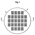
- Figure 1 is a plan view of a holder for electroconductive contact units in a contact probe embodying the present invention.
- the holder 1 may consist of a disk having a diameter of eight inches (approximately 200 mm).
- An 8-inch wafer typically produces tens to hundreds of semiconductor chips.
- a 12-inch wafer (approximately 300 mm) typically produces thousands of semiconductor chips.
- the holder 1 for an electroconductive contact probe is circular in shape in plan view similarly as the wafer that is to be tested, and is provided with a plurality of holder holes 2 for receiving a plurality of electroconductive contact units at positions that correspond to the electrodes of the chips formed in the wafer as is the case with the prior art.
- the holder holes 2 are illustrated in a somewhat exaggerated manner, and are smaller in number than actually are.
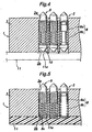
- Figure 2 is a fragmentary longitudinal sectional view taken along line II-II of Figure 1 showing exemplary electroconductive contact units embodying the present invention.
- three support members 3, 4 and 5 in the form of plate members having a same shape as seen in the plan view of Figure 1 are layered as an upper, middle and lower layer so as to form a three-layered holder for an electroconductive contact probe.
- the support members 3, 4 and 5 may be all made of a same material such as plastic material that allows the holder holes 2 to be formed at high precision or ceramic material that is highly resistant to heat. Metallic materials and semiconductor materials may also be used if necessary insulation is made by insert molding, coating or deposition of insulating material in required places.
- the support members 3, 4 and 5 are all provided with a conformal circular disk shape, and are held in position in the laminated state illustrated in Figure 2 by using threaded bolts or the like not shown in the drawing. The use of threaded bolts for securing the laminated assembly allows the assembly to be taken apart and reassembled with ease for maintenance and other purposes.
- one of the outer (upper in Figure 2 ) support member 3 is formed with stepped diameter holes each including a small diameter hole 2a and a large diameter hole 2b coaxially disposed to each other, and the other support members 4 and 5 are formed with straight holes 2c and 2d having a same diameter as the large diameter hole 2b.
- Each holder hole 2 thus consists of the corresponding stepped diameter hole 2a and 2b and the corresponding straight holes 2c and 2d.
- each contact unit comprises an electroconductive coil spring 8 and a pair of electroconductive contact members consisting of electroconductive needle members 9 and 10 provided on either end of the coil spring 8 with their free ends directed away from each other.
- One of the needle members 9 (or the lower needle member in Figure 3 ) comprises a needle portion 9a having a pointed end that is directed downward in Figure 3 , a flange portion 9b formed at the base end of the needle portion 9a and having an enlarged diameter as compared with the needle portion 9a, and a boss portion 9c projecting from the flange portion 9b away from the needle portion 9a (upward in Figure 3 ) all of which are disposed coaxial to one another.
- the other needle member 10 (or the upper needle member in Figure 3 ) comprises a needle portion 10a having a pointed end that is directed upward in Figure 3 , a boss portion 10b formed at the base end of the needle portion 10a and having a smaller diameter than the needle portion 10a, and a stem portion 10c projecting from the boss portion 10b away from the needle portion 10a (downward in Figure 3 ) all of which are again disposed coaxial to one another.
- the coil spring 8 comprises a closely wound portion 8a in a lower part thereof and a coarsely would portion 8b in an upper part thereof as seen in Figure 3 .
- the boss portion 9c of one of the needle member 9 fits into the coil end defined by the closely wound portion 8a, and the boss portion 10b of the other needle member 10 fits into the other coil end defined by the coarsely wound portion 8b.
- These boss portions 9c and 10b may be engaged by the corresponding ends of the coil spring 8 by virtue of the winding or wrapping force of the coil spring or by solder. When solder is used, the fit between the boss portions 9c and 10b and the corresponding coil ends may be a loose one.
- the free end of the stem portion 10c substantially coincides with the end of the closely wound portion 8a adjoining the coarsely wound portion 8b.
- the closely wound portion 8a comes into contact with the stem portion 10c so that the electric signal conducted between the two needle members 9 and 10 is allowed to flow through the closely wound portion 8a and stem portion 10c without flowing through the coarsely would portion 8b.
- the electric signal is allowed to flow axially or straight between the two needle members 9 and 10, and this makes the contact unit highly desirable for the testing of new generation chips involving high frequencies.
- the integrally joined assembly of the coil spring 8 and electroconductive needle members 9 and 10 is installed in the support members 3, 4 and 5 by introducing it into the holder hole 2 as indicated by an arrow in Figure 3 .
- the contact unit may be used either in an inverted orientation as illustrated in Figure 3 or in the normal orientation illustrated in Figure 2 .
- the assembly is prevented from coming off from the holder hole 2 by the flange portion 9b of one of the needle members 9 being engaged by the shoulder defined between the small diameter hole 2a and large diameter hole 2b.
- the shoulder defined between the small diameter hole 2a and large diameter hole 2b and the flange portion 9b prevents the assembly from coming off in one direction (downward direction in Figure 3 ).
- the circuit board 11 of the testing device is attached to the lower side of the contact probe, for instance by using threaded bolts with the stepped diameter hole 2a and 2b of the holder 1 facing up and the straight holes 2c and 2d of the holder 1 facing down.
- the circuit board 11 is provided with terminals 11a at positions corresponding to the needle members 10.
- the needle portion 10a of each needle member 10 engages the corresponding terminal 11a, and this prevents the assembly consisting of the coil spring 8 and needle members 9 and 10 from coming off from the holder hole 2 in the other direction.
- the terminals 11a of the circuit board 11 attached to the holder 1 are substantially flush with the lower surface of the holder 1 in the drawing, the part of each contact unit extending between the flange portion 9b and the needle portion 10a is accommodated in the large diameter hole 2b, 2c and 2d having the depth D. Also, because the length L and depth D are substantially equal to each other, substantially no significant load is applied to the coil spring 8 in the assembled state illustrated in Figure 2 . Therefore, the support member 3 remote from the circuit board 11 would not be pushed up by the spring force of the coil spring 8, and warping or deflecting of the support member 3 can be avoided even when the thickness of the support member 3 is small, for instance in the order of 1 mm, as opposed to the conventional arrangement. For this reason, this embodiment is highly beneficial for use in larger holders (having a diameter in the range of 200 to 300 mm).
- the length L may be slightly small than the depth D.
- the length L may be slightly greater than the depth D so that the needle portion 9a of each needle member slightly projects from the holder hole, and favorably accommodate such variations.
- the thickness of the support member 3 can be minimized.
- ceramic material or other insulating material having a low coefficient of thermal expansion can be used for the support member 3. Ceramic material is generally brittle, but the structure of the present invention can prevent the support member 3 made of such material from cracking, chipping or being otherwise damaged.
- the contact probe can be safely used for conducting bum-in tests which involve application of voltages under high temperature environments (approximately 150°C) for a prolonged periods of time (from few hours to tens of hours). In short, because the requirement of mechanical strength for the support members can be lowered, the freedom in the selection of the material for the support member is increased.
- the relationship between the length L and depth D may be selected in such a manner that the projecting length of the needle portion 10a out of the holder 1 (toward the circuit board 11) may be made as small as possible in the installed state of each contact unit consisting of the coil spring 8 and needle members 9 and 10 or the needle portion 10a barely touches the circuit board 11 with the needle portion 10a even slightly retracted from the outer surface of the holder 1. In any event, it is desirable to minimize the pressure (spring load) of the needle portion 10a on the terminal 11a when the circuit board 11 is assembled.
- any defects in the assembly can be readily detected, and the state of the coil springs 8 and needle members 9 and 10 can be easily verified.
- the contact probe holder was provided with a three-layered structure including three support members 3, 4 and 5, but may also consist of a single support member depending on the size and pitch of the holder holes.
- Such a single layered structure is illustrated in Figure 4 .
- the support member 3 shown in Figure 4 may be similar to the support member 3 of the previous embodiment, and the parts corresponding to those of the previous embodiment are denoted with like numerals without repeating the description of such parts.
- the contact probe holder illustrated in Figure 4 is provided with holder holes 2 each defined by a stepped diameter hole formed in a single support member 3, and a coil spring 8 and a pair of electroconductive needle members 9 and 10 are received in each holder hole 2.
- holder holes 2 each defined by a stepped diameter hole formed in a single support member 3, and a coil spring 8 and a pair of electroconductive needle members 9 and 10 are received in each holder hole 2.
- the coarsely wound portion 8b of each coil spring 8 is not required to be so long, and the holder 1 may consist of a single-layered structure including only one support member 3. In such a case, the thickness of the holder 1 can be reduced even further.
- Electroconductive contact members on either end of each coil spring 8 consisted of a pair of needle members 9 and 10 in the foregoing embodiments, but the contact members on one end of each coil spring 8 facing the circuit board 11 may consist of a coil end 12 (the coil end of the coarsely wound portion in the illustrated embodiment) as illustrated in Figure 5 so as to apply this coil end 12 to the corresponding terminal 11a.
- FIG. 7 shows a part of a contact probe having two moveable ends.
- Each of the electroconductive contact units shown in the drawing is provided with an electroconductive compression coil spring 30 and a pair of electroconductive needle members 29 and 31 adjoining either end of each coil spring, and thereby provides two moveable ends.
- the holder for supporting these units is formed by laminating three plastic support members 28, 32 and 33.
- the upper support member 28 is provided with small diameter holes each receiving one of the needle members 29 of the corresponding contact unit in an axially slidable manner so as to move its free end into and out of the holder, and the corresponding coil spring is received in a large diameter hole provided in the middle support member 32 and a large diameter part of a stepped diameter hole provided in the lower support member 33.
- the other needle member 31 is slidably received in a small diameter portion of the stepped diameter hole provided in the lower support member so as to move its free end into and out of the holder.
- the upper needle member 29 is provided with a flange portion that is received in the large diameter hole of the middle support member 32 so as to prevent the lower needle member 29 from coming off from the holder.
- the compression coil springs 30 placed under an unstressed state. Therefore, the coil springs 30 would not apply a force that tends to push the upper and lower support members 28 and 33 away from each other.
- the compression springs are compressed between these two external parts, and the desired resilient engagement force is produced in each point of contact.
- This embodiment therefore minimizes the stress that is applied to the holder. Furthermore, placing the compression coil springs 30 under an unstressed condition additionally provides the benefit of simplifying the assembly process.
- the assembling of the contact probe requires the needle members 29 and 31 and compression coil springs 30 to be placed in the corresponding holder holes before joining the support members 28, 32 and 33 to one another. If the coil springs 30 were prestressed in the installed state, the support members 28, 32 and 33 must be joined to one another against the combined spring force of the compression coil springs, and this would significantly impairs the simplicity of the assembly work. On the other hand, according to the illustrated embodiment, there is no need to oppose the spring force when joining the support members 28, 32 and 33, and this simplifies the assembly work.
- each contact unit comprising an electroconductive coil spring and electroconductive contact members is installed in the corresponding holder hole with the coil spring placed substantially in an unstressed state
- the part that prevents the electroconductive contact member from coming off is not subjected to the compressive load of the coil spring. Therefore, even when the holder is made of a thin plate member and/or is not provided with favorable mechanical properties, warping, deflecting or breaking of the holder can be avoided as opposed to the prior art, and materials having a small coefficient of thermal expansion and other desired material properties such as ceramic material can be safely used for the holder.
- the contact probe can be safely used for conducting burn-in tests which involve application of voltages under high temperature environments (approximately 150°C) for a prolonged periods of time (from few hours to tens of hours) even when it is formed as a highly compact unit.
- a semiconductor package substrate When a semiconductor package substrate is to be tested, it may contain 3,000 or more pads (terminals or the like) in each square centimeter, and the combined spring force may be significant even though the spring force of each spring may be extremely small so that the holder in the form of a plate member could warp under such a load.
- the contact probe of the present invention as each coil spring provides substantially no spring load in the installed state, the total load is substantially zero, and the warping or other deformation of the holder can be avoided.
- the contact units are installed in the corresponding holder holes in such a manner that the free ends of the electroconductive contact members on one side of the holder are substantially flush with the outer surface of the holder, by inspecting the projecting lengths of the contact members from the outer surface of the holder in the installed state, any defects in the assembly can be readily detected.
- the electroconductive contact members on one side of the holder may each consist of a coil end of the electroconductive coil spring.
- one of the contact members consists of a needle member which is joined with the coil spring while the other contact member consists of a coil end.
Applications Claiming Priority (3)
| Application Number | Priority Date | Filing Date | Title |
|---|---|---|---|
| JP2002113691 | 2002-04-16 | ||
| JP2002113691 | 2002-04-16 | ||
| PCT/JP2003/004839 WO2003087854A1 (en) | 2002-04-16 | 2003-04-16 | Conductive contact |
Publications (3)
| Publication Number | Publication Date |
|---|---|
| EP1496368A1 EP1496368A1 (en) | 2005-01-12 |
| EP1496368A4 EP1496368A4 (en) | 2005-09-07 |
| EP1496368B1 true EP1496368B1 (en) | 2012-03-28 |
Family
ID=29243363
Family Applications (1)
| Application Number | Title | Priority Date | Filing Date |
|---|---|---|---|
| EP03723133A Expired - Lifetime EP1496368B1 (en) | 2002-04-16 | 2003-04-16 | Conductive contact |
Country Status (8)
| Country | Link |
|---|---|
| US (1) | US7463041B2 (ja) |
| EP (1) | EP1496368B1 (ja) |
| JP (1) | JP4639048B2 (ja) |
| KR (1) | KR20040103956A (ja) |
| CN (1) | CN100442057C (ja) |
| AU (1) | AU2003235190A1 (ja) |
| TW (1) | TWI297077B (ja) |
| WO (1) | WO2003087854A1 (ja) |
Families Citing this family (24)
| Publication number | Priority date | Publication date | Assignee | Title |
|---|---|---|---|---|
| US8754416B2 (en) * | 2005-11-25 | 2014-06-17 | The Hong Hong University of Science and Technology | Method for fabrication of active-matrix display panels |
| MY147876A (en) * | 2005-12-05 | 2013-01-31 | Nhk Spring Co Ltd | Probe card |
| JP4823667B2 (ja) * | 2005-12-05 | 2011-11-24 | 日本発條株式会社 | プローブカード |
| EP2093576A4 (en) * | 2006-12-15 | 2010-09-22 | Nhk Spring Co Ltd | CONDUCTIVE CONTACT SUPPORT, CONDUCTIVE CONTACT UNIT AND METHOD FOR MANUFACTURING A CONDUCTIVE CONTACT SUPPORT |
| EP2239587B1 (en) * | 2008-02-01 | 2017-12-27 | NHK Spring Co., Ltd. | Probe unit |
| CN101685133B (zh) * | 2008-09-27 | 2011-12-07 | 京元电子股份有限公司 | 集成电路元件测试设备及其测试方法 |
| US7874880B2 (en) * | 2009-02-26 | 2011-01-25 | Ironwood Electronics, Inc. | Adapter apparatus with sleeve spring contacts |
| JP2010243411A (ja) * | 2009-04-08 | 2010-10-28 | Japan Electronic Materials Corp | 垂直型プローブ |
| TW201111790A (en) * | 2009-09-16 | 2011-04-01 | Probeleader Co Ltd | High-frequency vertical probe card structure |
| JP5378273B2 (ja) * | 2010-03-12 | 2013-12-25 | 株式会社アドバンテスト | コンタクトプローブ及びソケット、チューブ状プランジャの製造方法、並びにコンタクトプローブの製造方法 |
| JPWO2011122068A1 (ja) * | 2010-03-30 | 2013-07-08 | 住友電気工業株式会社 | コンタクトプローブ、コンタクトプローブ連結体およびこれらの製造方法 |
| EP2418503B1 (en) * | 2010-07-14 | 2013-07-03 | Sensirion AG | Needle head |
| US7950933B1 (en) * | 2010-08-04 | 2011-05-31 | Hon Hai Precison Ind. Co., Ltd. | Electrical socket having contact terminals floatably arranged therein |
| KR20130010311A (ko) * | 2011-07-18 | 2013-01-28 | 주식회사 코리아 인스트루먼트 | 수직형 프로브 카드 |
| KR101348205B1 (ko) * | 2013-01-08 | 2014-01-10 | 주식회사 아이에스시 | 탐침장치 |
| TW201533449A (zh) * | 2014-02-24 | 2015-09-01 | Mpi Corp | 具有彈簧套筒式探針之探針裝置 |
| US9577375B2 (en) * | 2014-08-29 | 2017-02-21 | Advanced Interconnections Corp. | Connector alignment assembly |
| JP2017142080A (ja) * | 2016-02-08 | 2017-08-17 | 日本電産リード株式会社 | 接触端子、検査治具、及び検査装置 |
| JP6812018B2 (ja) * | 2016-07-28 | 2021-01-13 | 日本電産リード株式会社 | 検査治具、これを備えた基板検査装置、及び検査治具の製造方法 |
| JP6432017B2 (ja) * | 2016-11-30 | 2018-12-05 | 日本電産リード株式会社 | 接触端子、検査治具、及び検査装置 |
| JP7021874B2 (ja) * | 2017-06-28 | 2022-02-17 | 株式会社ヨコオ | コンタクトプローブ及び検査治具 |
| CN111585079A (zh) * | 2020-05-28 | 2020-08-25 | 苏州华旃航天电器有限公司 | 一体式的pogopin射频连接器探针 |
| US11355872B2 (en) * | 2020-09-21 | 2022-06-07 | TE Connectivity Services Gmbh | Mezzanine power pin for an electrical connector system |
| TWI747582B (zh) | 2020-10-29 | 2021-11-21 | 創意電子股份有限公司 | 檢測裝置 |
Citations (1)
| Publication number | Priority date | Publication date | Assignee | Title |
|---|---|---|---|---|
| US6208155B1 (en) * | 1998-01-27 | 2001-03-27 | Cerprobe Corporation | Probe tip and method for making electrical contact with a solder ball contact of an integrated circuit device |
Family Cites Families (30)
| Publication number | Priority date | Publication date | Assignee | Title |
|---|---|---|---|---|
| US4029375A (en) * | 1976-06-14 | 1977-06-14 | Electronic Engineering Company Of California | Miniature electrical connector |
| US4528500A (en) * | 1980-11-25 | 1985-07-09 | Lightbody James D | Apparatus and method for testing circuit boards |
| US4508405A (en) * | 1982-04-29 | 1985-04-02 | Augat Inc. | Electronic socket having spring probe contacts |
| JPS63161366U (ja) * | 1987-04-10 | 1988-10-21 | ||
| US5225777A (en) * | 1992-02-04 | 1993-07-06 | International Business Machines Corporation | High density probe |
| US5414369A (en) * | 1992-11-09 | 1995-05-09 | Nhk Spring Co., Ltd. | Coil spring-pressed needle contact probe modules with offset needles |
| JP2532331B2 (ja) | 1992-11-09 | 1996-09-11 | 日本発条株式会社 | 導電性接触子 |
| US5395249A (en) * | 1993-06-01 | 1995-03-07 | Westinghouse Electric Corporation | Solder-free backplane connector |
| US6034532A (en) * | 1993-07-01 | 2000-03-07 | Alphatest Corporation | Resilient connector having a tubular spring |
| JP2997155B2 (ja) | 1993-08-13 | 2000-01-11 | ヒロセ電機株式会社 | 接触端子及び電気コネクタ |
| JPH08160075A (ja) * | 1994-12-09 | 1996-06-21 | Nhk Spring Co Ltd | 導電性接触子ユニット |
| JP2648120B2 (ja) | 1995-02-08 | 1997-08-27 | 山一電機株式会社 | 表面接触形接続器 |
| US5945837A (en) * | 1995-10-10 | 1999-08-31 | Xilinx, Inc. | Interface structure for an integrated circuit device tester |
| JP3342789B2 (ja) | 1995-10-25 | 2002-11-11 | 日本発条株式会社 | 導電性接触子 |
| CH693478A5 (fr) * | 1996-05-10 | 2003-08-15 | E Tec Ag | Socle de connexion de deux composants électriques. |
| US5825616A (en) * | 1997-01-21 | 1998-10-20 | Dell Usa, L.P. | Media module locking and ejecting mechanism |
| JPH10214649A (ja) | 1997-01-30 | 1998-08-11 | Yokowo Co Ltd | スプリングコネクタおよび該スプリングコネクタを用いた装置 |
| US6204680B1 (en) * | 1997-04-15 | 2001-03-20 | Delaware Capital Formation, Inc. | Test socket |
| US5955888A (en) * | 1997-09-10 | 1999-09-21 | Xilinx, Inc. | Apparatus and method for testing ball grid array packaged integrated circuits |
| GB2330009B (en) * | 1997-09-27 | 2001-11-28 | Nec Technologies | Method of electrically connecting a component to a PCB |
| US6556033B1 (en) * | 1998-07-10 | 2003-04-29 | Nhk Spring Co., Ltd. | Electroconductive contact unit assembly |
| EP1113275B1 (en) | 1998-07-10 | 2006-08-30 | Nhk Spring Co.Ltd. | Conductive contact |
| JP4124520B2 (ja) * | 1998-07-30 | 2008-07-23 | 日本発条株式会社 | 導電性接触子のホルダ及びその製造方法 |
| JP4187121B2 (ja) | 1998-12-02 | 2008-11-26 | 東プレ株式会社 | ピン状ボスのプレス成形方法 |
| JP3597738B2 (ja) | 1999-03-12 | 2004-12-08 | 日本発条株式会社 | 導電性接触子及び導電性接触子アセンブリ |
| JP2001116791A (ja) * | 1999-10-20 | 2001-04-27 | Fujitsu Ltd | 電子部品試験装置及び電気接続体 |
| US6341962B1 (en) | 1999-10-29 | 2002-01-29 | Aries Electronics, Inc. | Solderless grid array connector |
| JP3500105B2 (ja) * | 2000-02-10 | 2004-02-23 | 日本発条株式会社 | 導電性接触子用支持体及びコンタクトプローブユニット |
| JP2002202321A (ja) | 2000-12-28 | 2002-07-19 | Yokowo Co Ltd | 導電接触ピンおよびこのピンを用いたテストヘッド |
| JP5075309B2 (ja) * | 2001-03-16 | 2012-11-21 | 日本発條株式会社 | 導電性接触子用支持体 |
-
2003
- 2003-04-16 WO PCT/JP2003/004839 patent/WO2003087854A1/ja active Application Filing
- 2003-04-16 US US10/510,657 patent/US7463041B2/en not_active Expired - Lifetime
- 2003-04-16 EP EP03723133A patent/EP1496368B1/en not_active Expired - Lifetime
- 2003-04-16 KR KR10-2004-7016567A patent/KR20040103956A/ko not_active Application Discontinuation
- 2003-04-16 TW TW092108909A patent/TWI297077B/zh not_active IP Right Cessation
- 2003-04-16 JP JP2003584742A patent/JP4639048B2/ja not_active Expired - Lifetime
- 2003-04-16 AU AU2003235190A patent/AU2003235190A1/en not_active Abandoned
- 2003-04-16 CN CNB038085267A patent/CN100442057C/zh not_active Expired - Lifetime
Patent Citations (1)
| Publication number | Priority date | Publication date | Assignee | Title |
|---|---|---|---|---|
| US6208155B1 (en) * | 1998-01-27 | 2001-03-27 | Cerprobe Corporation | Probe tip and method for making electrical contact with a solder ball contact of an integrated circuit device |
Also Published As
| Publication number | Publication date |
|---|---|
| US20050237070A1 (en) | 2005-10-27 |
| TWI297077B (en) | 2008-05-21 |
| EP1496368A4 (en) | 2005-09-07 |
| US7463041B2 (en) | 2008-12-09 |
| WO2003087854A1 (en) | 2003-10-23 |
| CN100442057C (zh) | 2008-12-10 |
| TW200306424A (en) | 2003-11-16 |
| KR20040103956A (ko) | 2004-12-09 |
| EP1496368A1 (en) | 2005-01-12 |
| JP4639048B2 (ja) | 2011-02-23 |
| JPWO2003087854A1 (ja) | 2005-08-25 |
| AU2003235190A1 (en) | 2003-10-27 |
| CN1646922A (zh) | 2005-07-27 |
Similar Documents
| Publication | Publication Date | Title |
|---|---|---|
| EP1496368B1 (en) | Conductive contact | |
| EP0995996B1 (en) | Conductive contact | |
| US7898272B2 (en) | Probe card | |
| JP4920769B2 (ja) | 導電性接触子用ホルダ | |
| KR100691680B1 (ko) | 반도체 장치 시험용 콘택터 및 그 제조 방법 | |
| US6566898B2 (en) | Temperature compensated vertical pin probing device | |
| US6297657B1 (en) | Temperature compensated vertical pin probing device | |
| US6642728B1 (en) | Holder of electroconductive contactor, and method for producing the same | |
| US6420887B1 (en) | Modulated space transformer for high density buckling beam probe and method for making the same | |
| EP1496367B1 (en) | Holder for conductive contact | |
| JP3500105B2 (ja) | 導電性接触子用支持体及びコンタクトプローブユニット | |
| US20040051546A1 (en) | Temperature compensated vertical pin probing device | |
| JP2010060316A (ja) | 異方性導電部材および異方導電性を有する測定用基板 | |
| EP1194784B1 (en) | Temperature compensated vertical pin probing device | |
| US7053635B2 (en) | Support member assembly for electroconductive contact members | |
| KR20040012987A (ko) | 지지체 어셈블리 | |
| JP2011252916A (ja) | 導電性接触子用支持体 |
Legal Events
| Date | Code | Title | Description |
|---|---|---|---|
| PUAI | Public reference made under article 153(3) epc to a published international application that has entered the european phase |
Free format text: ORIGINAL CODE: 0009012 |
|
| 17P | Request for examination filed |
Effective date: 20041008 |
|
| AK | Designated contracting states |
Kind code of ref document: A1 Designated state(s): AT BE BG CH CY CZ DE DK EE ES FI FR GB GR HU IE IT LI LU MC NL PT RO SE SI SK TR |
|
| AX | Request for extension of the european patent |
Extension state: AL LT LV MK |
|
| A4 | Supplementary search report drawn up and despatched |
Effective date: 20050727 |
|
| GRAP | Despatch of communication of intention to grant a patent |
Free format text: ORIGINAL CODE: EPIDOSNIGR1 |
|
| GRAS | Grant fee paid |
Free format text: ORIGINAL CODE: EPIDOSNIGR3 |
|
| GRAA | (expected) grant |
Free format text: ORIGINAL CODE: 0009210 |
|
| AK | Designated contracting states |
Kind code of ref document: B1 Designated state(s): DE IT |
|
| REG | Reference to a national code |
Ref country code: DE Ref legal event code: R096 Ref document number: 60340408 Country of ref document: DE Effective date: 20120524 |
|
| PLBE | No opposition filed within time limit |
Free format text: ORIGINAL CODE: 0009261 |
|
| STAA | Information on the status of an ep patent application or granted ep patent |
Free format text: STATUS: NO OPPOSITION FILED WITHIN TIME LIMIT |
|
| PG25 | Lapsed in a contracting state [announced via postgrant information from national office to epo] |
Ref country code: IT Free format text: LAPSE BECAUSE OF FAILURE TO SUBMIT A TRANSLATION OF THE DESCRIPTION OR TO PAY THE FEE WITHIN THE PRESCRIBED TIME-LIMIT Effective date: 20120328 |
|
| 26N | No opposition filed |
Effective date: 20130103 |
|
| REG | Reference to a national code |
Ref country code: DE Ref legal event code: R097 Ref document number: 60340408 Country of ref document: DE Effective date: 20130103 |
|
| PGFP | Annual fee paid to national office [announced via postgrant information from national office to epo] |
Ref country code: DE Payment date: 20220302 Year of fee payment: 20 |
|
| REG | Reference to a national code |
Ref country code: DE Ref legal event code: R071 Ref document number: 60340408 Country of ref document: DE |