EP1480082B1 - Ringfeld-4-Spiegelsysteme mit konvexem Primärspiegel für die EUV-Lithographie - Google Patents
Ringfeld-4-Spiegelsysteme mit konvexem Primärspiegel für die EUV-Lithographie Download PDFInfo
- Publication number
- EP1480082B1 EP1480082B1 EP04018664A EP04018664A EP1480082B1 EP 1480082 B1 EP1480082 B1 EP 1480082B1 EP 04018664 A EP04018664 A EP 04018664A EP 04018664 A EP04018664 A EP 04018664A EP 1480082 B1 EP1480082 B1 EP 1480082B1
- Authority
- EP
- European Patent Office
- Prior art keywords
- mirror
- reduction objective
- objective according
- systems
- convex
- Prior art date
- Legal status (The legal status is an assumption and is not a legal conclusion. Google has not performed a legal analysis and makes no representation as to the accuracy of the status listed.)
- Expired - Lifetime
Links
- 238000001900 extreme ultraviolet lithography Methods 0.000 title description 5
- 230000009467 reduction Effects 0.000 claims description 18
- 230000003287 optical effect Effects 0.000 claims description 11
- 230000005540 biological transmission Effects 0.000 claims description 6
- 238000000034 method Methods 0.000 claims description 4
- 238000001393 microlithography Methods 0.000 claims description 4
- 238000004519 manufacturing process Methods 0.000 claims description 3
- 238000013461 design Methods 0.000 description 10
- 238000003384 imaging method Methods 0.000 description 6
- 238000012937 correction Methods 0.000 description 5
- 238000002310 reflectometry Methods 0.000 description 5
- 206010065042 Immune reconstitution inflammatory syndrome Diseases 0.000 description 3
- 238000001459 lithography Methods 0.000 description 3
- 238000009304 pastoral farming Methods 0.000 description 3
- 230000005855 radiation Effects 0.000 description 3
- 230000003068 static effect Effects 0.000 description 3
- 230000008569 process Effects 0.000 description 2
- 210000001747 pupil Anatomy 0.000 description 2
- ZOKXTWBITQBERF-UHFFFAOYSA-N Molybdenum Chemical compound [Mo] ZOKXTWBITQBERF-UHFFFAOYSA-N 0.000 description 1
- 230000004075 alteration Effects 0.000 description 1
- 230000008901 benefit Effects 0.000 description 1
- 230000015556 catabolic process Effects 0.000 description 1
- 230000008859 change Effects 0.000 description 1
- 238000000576 coating method Methods 0.000 description 1
- 238000010276 construction Methods 0.000 description 1
- 230000007423 decrease Effects 0.000 description 1
- 238000006731 degradation reaction Methods 0.000 description 1
- 238000011161 development Methods 0.000 description 1
- 238000009826 distribution Methods 0.000 description 1
- 230000000694 effects Effects 0.000 description 1
- 230000002349 favourable effect Effects 0.000 description 1
- 238000009434 installation Methods 0.000 description 1
- 229910052750 molybdenum Inorganic materials 0.000 description 1
- 239000011733 molybdenum Substances 0.000 description 1
- 230000010287 polarization Effects 0.000 description 1
- 230000009257 reactivity Effects 0.000 description 1
- 239000000758 substrate Substances 0.000 description 1
- 238000012549 training Methods 0.000 description 1
- 230000007704 transition Effects 0.000 description 1
Images


Classifications
-
- G—PHYSICS
- G02—OPTICS
- G02B—OPTICAL ELEMENTS, SYSTEMS OR APPARATUS
- G02B17/00—Systems with reflecting surfaces, with or without refracting elements
- G02B17/02—Catoptric systems, e.g. image erecting and reversing system
- G02B17/06—Catoptric systems, e.g. image erecting and reversing system using mirrors only, i.e. having only one curved mirror
-
- G—PHYSICS
- G03—PHOTOGRAPHY; CINEMATOGRAPHY; ANALOGOUS TECHNIQUES USING WAVES OTHER THAN OPTICAL WAVES; ELECTROGRAPHY; HOLOGRAPHY
- G03F—PHOTOMECHANICAL PRODUCTION OF TEXTURED OR PATTERNED SURFACES, e.g. FOR PRINTING, FOR PROCESSING OF SEMICONDUCTOR DEVICES; MATERIALS THEREFOR; ORIGINALS THEREFOR; APPARATUS SPECIALLY ADAPTED THEREFOR
- G03F7/00—Photomechanical, e.g. photolithographic, production of textured or patterned surfaces, e.g. printing surfaces; Materials therefor, e.g. comprising photoresists; Apparatus specially adapted therefor
- G03F7/70—Microphotolithographic exposure; Apparatus therefor
- G03F7/70216—Mask projection systems
- G03F7/70358—Scanning exposure, i.e. relative movement of patterned beam and workpiece during imaging
-
- G—PHYSICS
- G02—OPTICS
- G02B—OPTICAL ELEMENTS, SYSTEMS OR APPARATUS
- G02B17/00—Systems with reflecting surfaces, with or without refracting elements
- G02B17/02—Catoptric systems, e.g. image erecting and reversing system
- G02B17/06—Catoptric systems, e.g. image erecting and reversing system using mirrors only, i.e. having only one curved mirror
- G02B17/0647—Catoptric systems, e.g. image erecting and reversing system using mirrors only, i.e. having only one curved mirror using more than three curved mirrors
- G02B17/0663—Catoptric systems, e.g. image erecting and reversing system using mirrors only, i.e. having only one curved mirror using more than three curved mirrors off-axis or unobscured systems in which not all of the mirrors share a common axis of rotational symmetry, e.g. at least one of the mirrors is warped, tilted or decentered with respect to the other elements
-
- G—PHYSICS
- G03—PHOTOGRAPHY; CINEMATOGRAPHY; ANALOGOUS TECHNIQUES USING WAVES OTHER THAN OPTICAL WAVES; ELECTROGRAPHY; HOLOGRAPHY
- G03F—PHOTOMECHANICAL PRODUCTION OF TEXTURED OR PATTERNED SURFACES, e.g. FOR PRINTING, FOR PROCESSING OF SEMICONDUCTOR DEVICES; MATERIALS THEREFOR; ORIGINALS THEREFOR; APPARATUS SPECIALLY ADAPTED THEREFOR
- G03F7/00—Photomechanical, e.g. photolithographic, production of textured or patterned surfaces, e.g. printing surfaces; Materials therefor, e.g. comprising photoresists; Apparatus specially adapted therefor
- G03F7/70—Microphotolithographic exposure; Apparatus therefor
- G03F7/70216—Mask projection systems
- G03F7/70233—Optical aspects of catoptric systems, i.e. comprising only reflective elements, e.g. extreme ultraviolet [EUV] projection systems
-
- Y—GENERAL TAGGING OF NEW TECHNOLOGICAL DEVELOPMENTS; GENERAL TAGGING OF CROSS-SECTIONAL TECHNOLOGIES SPANNING OVER SEVERAL SECTIONS OF THE IPC; TECHNICAL SUBJECTS COVERED BY FORMER USPC CROSS-REFERENCE ART COLLECTIONS [XRACs] AND DIGESTS
- Y10—TECHNICAL SUBJECTS COVERED BY FORMER USPC
- Y10S—TECHNICAL SUBJECTS COVERED BY FORMER USPC CROSS-REFERENCE ART COLLECTIONS [XRACs] AND DIGESTS
- Y10S359/00—Optical: systems and elements
- Y10S359/90—Methods
Definitions
- the invention relates to a reduction objective according to the preamble of Claim 1, an exposure system according to claims 11 and 12 and a Chip manufacturing method according to claim 13.
- the systems In order to provide image formats of 26x34mm 2 or 26x52mm 2 , it is advantageous to form the systems as a ring field scanner.
- the usable secant length of the scan slot is then at least 26mm.
- the ring width should be in the range 0.5 - 2 mm to allow a homogeneous lighting or exposure control and 'can control'.
- Distortion distinguishes between static and dynamic or scan distortion. Scan distortion is the effective, by integrating the static distortion over the scan path resulting distortion. Limits for scale-corrected, static Distortion essentially results from the specifications for Contrast and CD variation.
- a telecentric beam path is not possible on the object side.
- transmission masks z.
- Stencilmasken used, a telecentric beam path can be realized.
- the image-side telecentricity means that the entrance pupil of the last mirror in or near its focal point, comes to rest. To one To obtain a compact design with an accessible aperture, it is advisable to use the To put the penultimate mirror as bundle limiting element there.
- the systems according to US Pat. No. 5,063,586 and EP 0 422 853 have a rectangular image field of, for example, at least 5 ⁇ 5 mm 2 .
- the generally decentered systems are subject to very high% distortion values.
- the lenses could therefore only be used in steppers with distortion control on the reticle.
- the high level of distortion makes such lenses impractical at the feature sizes discussed herein ( ⁇ 130 nm).
- the mirror sequence is convex, concave, convex, concave.
- the object of the invention is thus one for lithography with short Wavelengths, ⁇ 193 nm, preferably ⁇ 100 nm, suitable Projection objective to specify the disadvantages mentioned above of the prior art does not have, with as few optical Eliminates elements and on the other hand, a sufficiently large aperture and the Telezentriean petitionen and all others Requirement for a projection system for wavelengths ⁇ 193 nm.
- the object is achieved by a projection lens, the comprises four mirrors and by a convex primary mirror and a positive main beam angle magnification of the secondary mirror is.
- the 4-mirror lens according to the invention is thus characterized by high Resolution, low manufacturing costs and high throughput.
- the bezel is then physically accessible, the design compact and shadowing.
- the or additional mirror preferably aspherical derived from a plane surface Have surfaces.
- At least one mirror is an active mirror.
- the secondary mirror and the quaternary mirror are concave.
- the multilayer mirrors are convex-concave-convex-concave in order educated.
- the asphericities discussed in this document refer to the peak-to-peak or peak to valley (PV) deviation A of the aspheric surfaces opposite to the best-fitting sphere in the working area.
- PV peak to valley
- the information on the angles of incidence refers to the angle between each incident beam and surface normal at the point of incidence. Given is the largest angle of any beam, in general a beam limiting beam that occurs at any of the mirrors.
- the wafer-side optical free working distance is particularly preferred 60 mm.
- the reticle-side free working distance is at least 100 mm.
- the lenses described above can not only be used for EUV lithography be used, but of course in others Wavelengths, without departing from the invention. Becomes practical that only at UV wavelengths in the range around 193 nm with excimer lasers in To consider.
- the design portion of the rms wavefront component of the system is at most 0.07 ⁇ , preferably 0.03 ⁇ .
- the lenses are always formed telecentric on the image side.
- Projection lens object-side telecentric is designed.
- the telecentric error on the wafer should not be 10 mrad it is preferably 5 mrad, more preferably 2 mrad. This ensures that the change in magnification or the distortion over the depth of field range in tolerable Keeps borders.
- the invention reduction or Projection objective device also provides the invention Projection exposure apparatus comprising at least one such objective, to disposal.
- the Projection exposure system on a reflection mask in an alternative Embodiment of a transmission mask.
- the projection exposure apparatus has a Illuminating device for illuminating an off-axis ring field includes and the system is designed as a ring field scanner. Is an advantage provided that the secant length of the scan slot at least 26 mm is and the ring width is greater than 0.5 mm, so that a homogeneous Lighting is enabled.
- the aspherical Deviations from the best-fitting sphere are kept low, so that the demand for 'diffraction limit' and high reflectivity of ML mirrors with the resulting extreme accuracy requirements to these surfaces in all spatial frequency ranges of free diameter the mirror can be maintained down to atomic dimensions.
- DBRs distributed Bragg reflectors
- the lenses according to the invention by a lower average Angle of incidence and a small area-specific variation around the mean Angle of incidence can be the problems of Multilayer systems are kept low.
- M1 the primary mirror magnification m
- M2 the secondary mirror main beam angle enlargements
- main beam angle magnification or angular magnification refers not on the angle itself, but on its tangent (see Korsch, Reflective optics a.a.O.)
- Positive main beam angle magnification means vividly that the inclinations of those with the incident and reflected Principal rays identifiable straight lines with respect to the optical axis the same Sign, or, that the entrance and exit pupils of the concerned mirror lie on the same physical side of the mirror.
- the affiliation with the respective topological context is determined by ⁇ (M2).
- the ring field systems known from US 531629 and EP 0480617 belong to the category type a.
- Type b systems mediate the continuous transition to the type systems, which also includes that of Donald W. Sweeney et. al., 23rd International Symposium of Microlithography cited above.
- Type f and type g systems are not known from any of the publications cited. Compared to US 5315629 or EP 048 0617, the systems differ according to type f and type g by the convex primary mirror. This is from Donald W. Sweeney et. al. Although 23 rd International Symposium of Microlithography cited above known system has a convex primary mirror; however, has another major beam angle magnification on M2, and thus another beam steering in the system.
- Type f (94)
- M1 convex convex ⁇ (M1) -2.4 -2.9 ⁇ (M2) 0.6 1.6 N /
- FWD [mm] 92 62 CRAO [mm] ⁇ [-2.1, -2.0] ⁇ [4.1,4.2] CRA [mrad] ⁇ [-0.35.
- Ring field radius [mm] Image field radius in the middle of the ring field OO '[mm] Object-image distance FWD [mm] optically free working distance on the image side CRAO [deg] Main beam angle in the object space CRA [mrad] Main beam angle in the image space Max. Aspherical. [.Mu.m] Max. Deviation of the asphere from the enveloping circle over the useful range of the mirror AOI max. [Deg] maximum angle of incidence ⁇ AOI max [deg] Variation of angles of incidence across the mirror WFE max [ ⁇ rms] maximum rms wavefront error in units of ⁇ Distortion [nm PV] Peak-to-peak value of the main beam distortion scaled over the ring field
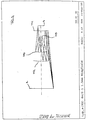
- FIG. 2 shows the section of a type e system from the reticle plane 2 to the wafer plane 4; the mirror closest to the mirror is the first mirror M1.
- Type_e systems have the lowest angular load on the mirrors M1, M2, M3, M4 what the polarization optical properties of the system favored. However, the high main beam angles at the reticle plane 2 require very flat reticles.
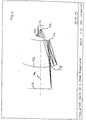
- type_g systems as exemplified in the section of FIG. 4, show shown at reasonable main beam angles at the reticle relatively large Angular loads on the mirrors M1, M2, M3, M4.
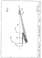
- Type_f systems as exemplified in FIG. 3, require the strongest Aspheres, but have favorable angular distributions on the mirrors, M1, M2, M3, M4, and the reticle 2.
- the very small distortion is relatively small field of view opposite.
- the overall length is larger than the other systems that allow long drift distance within the lens on the other hand, if necessary, the onset of additional components, eg. B. Alignment system, deflection mirrors, etc.
- the Type_f and Type_g systems can both with positive and negative main ray angles at the reticle 2 will be realized.
- This can be an optimal geometry, in particular a comparatively small free working distance to the reticle 2, for reflection of the light when using a reflection mask.
- at Using a transmission mask can be a telecentric Realize beam path.
- the systems of type_a and type_f have relatively long 'drift distances' or within the actual mirror system. It is possible there grazing-incidence mirror high reflectivity as Correction elements, eg. B. in the manner of a Schmidt corrector or an active insert optical correction system. Based on the current Literature values are given for molybdenum coated mirrors at 13.3 nm and 75 ° angle of incidence a theoretically possible reflectivity of about 85% for unpolarized light. By the grazing incidence of the bundle of the illuminated cross-section in one direction - compared to those on the neighboring mirrors - be made very large, what the interpretation facilitates the correction elements.
- the individual mirrors are preferably in pairs with mutually nearly perpendicular surface normals equipped to bundles in all directions with the same To manipulate resolution.
- a 4-mirror projection lens a magnification of preferably 4x for the preferred use in an EUV ring field projection system, both the necessary resolution at required image field as well Design conditions, which is a functional Construction allow, as the aspheres sufficiently mild, the angles sufficiently small for the layers and the installation space for the mirror support are sufficiently large.
Landscapes
- Physics & Mathematics (AREA)
- General Physics & Mathematics (AREA)
- Optics & Photonics (AREA)
- Lenses (AREA)
- Exposure Of Semiconductors, Excluding Electron Or Ion Beam Exposure (AREA)
- Exposure And Positioning Against Photoresist Photosensitive Materials (AREA)
Applications Claiming Priority (3)
| Application Number | Priority Date | Filing Date | Title |
|---|---|---|---|
| DE19824442 | 1998-05-30 | ||
| DE19824442 | 1998-05-30 | ||
| EP99110265A EP0962830A1 (de) | 1998-05-30 | 1999-05-27 | Ringfeld-4-Spiegelsysteme mit konvexem Primärspiegel für die EUV-Lithographie |
Related Parent Applications (2)
| Application Number | Title | Priority Date | Filing Date |
|---|---|---|---|
| EP99110265A Division EP0962830A1 (de) | 1998-05-30 | 1999-05-27 | Ringfeld-4-Spiegelsysteme mit konvexem Primärspiegel für die EUV-Lithographie |
| EP99110265.8 Division | 1999-05-27 |
Publications (2)
| Publication Number | Publication Date |
|---|---|
| EP1480082A1 EP1480082A1 (de) | 2004-11-24 |
| EP1480082B1 true EP1480082B1 (de) | 2005-11-30 |
Family
ID=7869552
Family Applications (2)
| Application Number | Title | Priority Date | Filing Date |
|---|---|---|---|
| EP04018664A Expired - Lifetime EP1480082B1 (de) | 1998-05-30 | 1999-05-27 | Ringfeld-4-Spiegelsysteme mit konvexem Primärspiegel für die EUV-Lithographie |
| EP99110265A Withdrawn EP0962830A1 (de) | 1998-05-30 | 1999-05-27 | Ringfeld-4-Spiegelsysteme mit konvexem Primärspiegel für die EUV-Lithographie |
Family Applications After (1)
| Application Number | Title | Priority Date | Filing Date |
|---|---|---|---|
| EP99110265A Withdrawn EP0962830A1 (de) | 1998-05-30 | 1999-05-27 | Ringfeld-4-Spiegelsysteme mit konvexem Primärspiegel für die EUV-Lithographie |
Country Status (6)
| Country | Link |
|---|---|
| US (1) | US6244717B1 (enExample) |
| EP (2) | EP1480082B1 (enExample) |
| JP (1) | JP2000031041A (enExample) |
| KR (1) | KR100568758B1 (enExample) |
| DE (2) | DE19923609A1 (enExample) |
| TW (1) | TW512238B (enExample) |
Families Citing this family (48)
| Publication number | Priority date | Publication date | Assignee | Title |
|---|---|---|---|---|
| US7186983B2 (en) | 1998-05-05 | 2007-03-06 | Carl Zeiss Smt Ag | Illumination system particularly for microlithography |
| DE19903807A1 (de) | 1998-05-05 | 1999-11-11 | Zeiss Carl Fa | Beleuchtungssystem insbesondere für die EUV-Lithographie |
| US6947124B2 (en) | 1998-05-05 | 2005-09-20 | Carl Zeiss Smt Ag | Illumination system particularly for microlithography |
| US6438199B1 (en) * | 1998-05-05 | 2002-08-20 | Carl-Zeiss-Stiftung | Illumination system particularly for microlithography |
| DE10138313A1 (de) * | 2001-01-23 | 2002-07-25 | Zeiss Carl | Kollektor für Beleuchtugnssysteme mit einer Wellenlänge < 193 nm |
| US20050002090A1 (en) * | 1998-05-05 | 2005-01-06 | Carl Zeiss Smt Ag | EUV illumination system having a folding geometry |
| US6859328B2 (en) * | 1998-05-05 | 2005-02-22 | Carl Zeiss Semiconductor | Illumination system particularly for microlithography |
| US6577443B2 (en) * | 1998-05-30 | 2003-06-10 | Carl-Zeiss Stiftung | Reduction objective for extreme ultraviolet lithography |
| US6831963B2 (en) * | 2000-10-20 | 2004-12-14 | University Of Central Florida | EUV, XUV, and X-Ray wavelength sources created from laser plasma produced from liquid metal solutions |
| EP1093021A3 (en) | 1999-10-15 | 2004-06-30 | Nikon Corporation | Projection optical system as well as equipment and methods making use of said system |
| TW538256B (en) | 2000-01-14 | 2003-06-21 | Zeiss Stiftung | Microlithographic reduction projection catadioptric objective |
| EP2081086B1 (en) * | 2000-11-07 | 2013-01-02 | ASML Netherlands B.V. | Lithographic apparatus and device manufacturing method |
| TW573234B (en) * | 2000-11-07 | 2004-01-21 | Asml Netherlands Bv | Lithographic projection apparatus and integrated circuit device manufacturing method |
| JP2003045782A (ja) | 2001-07-31 | 2003-02-14 | Canon Inc | 反射型縮小投影光学系及びそれを用いた露光装置 |
| DE10139188A1 (de) | 2001-08-16 | 2003-03-06 | Schott Glas | Glaskeramik für röntgenoptische Komponenten |
| JP2003233002A (ja) * | 2002-02-07 | 2003-08-22 | Canon Inc | 反射型投影光学系、露光装置及びデバイス製造方法 |
| US7084412B2 (en) * | 2002-03-28 | 2006-08-01 | Carl Zeiss Smt Ag | Collector unit with a reflective element for illumination systems with a wavelength of smaller than 193 nm |
| EP1446813B1 (de) * | 2002-05-10 | 2010-11-10 | Carl Zeiss SMT AG | Reflektives roentgenmikroskop zur untersuchung von objekten mit wellenlaengen = 100nm in reflexion |
| JP3919599B2 (ja) * | 2002-05-17 | 2007-05-30 | キヤノン株式会社 | 光学素子、当該光学素子を有する光源装置及び露光装置 |
| US6975385B2 (en) | 2002-11-08 | 2005-12-13 | Canon Kabushiki Kaisha | Projection optical system and exposure apparatus |
| WO2004066287A1 (en) | 2003-01-23 | 2004-08-05 | Lg Electronics Inc. | Recording medium with an optional information and apparatus and methods for forming, recording, reproducing and controlling reproduction of the recording medium |
| US20040148790A1 (en) * | 2003-02-04 | 2004-08-05 | Taiwan Semiconductor Manufacturing Company | Time alarm system in detecting scanner/step module tilt |
| US20040157944A1 (en) * | 2003-02-07 | 2004-08-12 | China Textile Institute | Preparation method for foaming waterborne PU |
| DE10321103A1 (de) * | 2003-05-09 | 2004-12-02 | Carl Zeiss Smt Ag | Verfahren zur Vermeidung von Kontamination und EUV-Lithographievorrichtung |
| US8208198B2 (en) | 2004-01-14 | 2012-06-26 | Carl Zeiss Smt Gmbh | Catadioptric projection objective |
| US7466489B2 (en) | 2003-12-15 | 2008-12-16 | Susanne Beder | Projection objective having a high aperture and a planar end surface |
| WO2005059645A2 (en) | 2003-12-19 | 2005-06-30 | Carl Zeiss Smt Ag | Microlithography projection objective with crystal elements |
| KR101150037B1 (ko) | 2004-01-14 | 2012-07-02 | 칼 짜이스 에스엠티 게엠베하 | 반사굴절식 투영 대물렌즈 |
| US7463422B2 (en) | 2004-01-14 | 2008-12-09 | Carl Zeiss Smt Ag | Projection exposure apparatus |
| US20080151364A1 (en) | 2004-01-14 | 2008-06-26 | Carl Zeiss Smt Ag | Catadioptric projection objective |
| KR20170129271A (ko) | 2004-05-17 | 2017-11-24 | 칼 짜이스 에스엠티 게엠베하 | 중간이미지를 갖는 카타디옵트릭 투사 대물렌즈 |
| DE102005042005A1 (de) | 2004-12-23 | 2006-07-06 | Carl Zeiss Smt Ag | Hochaperturiges Objektiv mit obskurierter Pupille |
| EP1889110A1 (en) * | 2005-05-13 | 2008-02-20 | Carl Zeiss SMT AG | A six-mirror euv projection system with low incidence angles |
| KR100962911B1 (ko) * | 2005-09-13 | 2010-06-10 | 칼 짜이스 에스엠테 아게 | 마이크로리소그라피 투영 광학 시스템, 디바이스 제작 방법 및 광학 표면을 설계하기 위한 방법 |
| DE102005056914A1 (de) | 2005-11-29 | 2007-05-31 | Carl Zeiss Smt Ag | Projektionsbelichtungsystem |
| JP5068271B2 (ja) | 2006-02-17 | 2012-11-07 | カール・ツァイス・エスエムティー・ゲーエムベーハー | マイクロリソグラフィ照明システム、及びこの種の照明システムを含む投影露光装置 |
| DE102006014380A1 (de) * | 2006-03-27 | 2007-10-11 | Carl Zeiss Smt Ag | Projektionsobjektiv und Projektionsbelichtungsanlage mit negativer Schnittweite der Eintrittspupille |
| JP5479890B2 (ja) | 2006-04-07 | 2014-04-23 | カール・ツァイス・エスエムティー・ゲーエムベーハー | マイクロリソグラフィ投影光学システム、装置、及び製造方法 |
| DE102007023411A1 (de) * | 2006-12-28 | 2008-07-03 | Carl Zeiss Smt Ag | Optisches Element, Beleuchtungsoptik für die Mikrolithographie mit mindestens einem derartigen optischen Element sowie Beleuchtungssystem mit einer derartigen Beleuchtungsoptik |
| EP1950594A1 (de) | 2007-01-17 | 2008-07-30 | Carl Zeiss SMT AG | Abbildende Optik, Projektionsbelichtunsanlage für die Mikrolithographie mit einer derartigen abbildenden Optik, Verfahren zur Herstellung eines mikrostrukturierten Bauteils mit einer derartigen Projektionsbelichtungsanlage, durch das Herstellungsverfahren gefertigtes mikrostrukturiertes Bauelement sowie Verwendung einer derartigen abbildenden Optik |
| DE102007047109A1 (de) | 2007-10-01 | 2009-04-09 | Carl Zeiss Smt Ag | Optisches System, insbesondere Projektionsobjektiv der Mikrolithographie |
| JP2009179391A (ja) * | 2008-01-31 | 2009-08-13 | Yoshino Kogyosho Co Ltd | 簡易開蓋キャップ |
| JP4935886B2 (ja) * | 2009-12-10 | 2012-05-23 | 三菱電機株式会社 | 画像読取装置 |
| DE102012202675A1 (de) * | 2012-02-22 | 2013-01-31 | Carl Zeiss Smt Gmbh | Abbildende Optik sowie Projektionsbelichtungsanlage für die Projektionslithografie mit einer derartigen abbildenden Optik |
| US9291751B2 (en) | 2013-06-17 | 2016-03-22 | Carl Zeiss Smt Gmbh | Imaging optical unit and projection exposure apparatus for projection lithography comprising such an imaging optical unit |
| DE102014208770A1 (de) * | 2013-07-29 | 2015-01-29 | Carl Zeiss Smt Gmbh | Projektionsoptik zur Abbildung eines Objektfeldes in ein Bildfeld sowie Projektionsbelichtungsanlage mit einer derartigen Projektionsoptik |
| DE102015221984A1 (de) * | 2015-11-09 | 2017-05-11 | Carl Zeiss Smt Gmbh | Abbildende Optik zur Abbildung eines Objektfeldes in ein Bildfeld sowie Projektionsbelichtungsanlage mit einer derartigen abbildenden Optik |
| CN118627208B (zh) * | 2024-05-11 | 2025-10-24 | 南京航空航天大学 | 非静力大气掠入射积分数值计算方法 |
Family Cites Families (27)
| Publication number | Priority date | Publication date | Assignee | Title |
|---|---|---|---|---|
| DE501365C (de) | 1930-07-01 | Walter Stoye | Verbindung, insbesondere der die Wagenkastenwaende bildenden Bleche mit dem aus I-Profilstaeben gebildeten Wagenkastengerippe, insbesondere fuer Kraftfahrzeuge | |
| BE369232A (enExample) | 1929-04-13 | |||
| DE701652C (enExample) | 1937-04-16 | 1941-01-21 | Gerhard Zur Nedden | |
| US2970518A (en) * | 1958-12-29 | 1961-02-07 | Karl F Ross | Catoptric system |
| US3748015A (en) * | 1971-06-21 | 1973-07-24 | Perkin Elmer Corp | Unit power imaging catoptric anastigmat |
| CH543009A (de) | 1972-08-25 | 1973-10-15 | Kuehlmoebelfabrik Alfons Laemm | Einrichtung zur Verbindung baukastenartig aneinandergefügter Kühlmöbel-Baueinheiten |
| US4861148A (en) * | 1986-03-12 | 1989-08-29 | Matsushita Electric Industrial Co., Inc. | Projection optical system for use in precise copy |
| US4804258A (en) * | 1986-05-05 | 1989-02-14 | Hughes Aircraft Company | Four mirror afocal wide field of view optical system |
| EP0252734B1 (en) * | 1986-07-11 | 2000-05-03 | Canon Kabushiki Kaisha | X-ray reduction projection exposure system of reflection type |
| US5071240A (en) * | 1989-09-14 | 1991-12-10 | Nikon Corporation | Reflecting optical imaging apparatus using spherical reflectors and producing an intermediate image |
| US5063586A (en) * | 1989-10-13 | 1991-11-05 | At&T Bell Laboratories | Apparatus for semiconductor lithography |
| US5315629A (en) * | 1990-10-10 | 1994-05-24 | At&T Bell Laboratories | Ringfield lithography |
| JPH04333011A (ja) * | 1991-05-09 | 1992-11-20 | Nikon Corp | 反射縮小投影光学装置 |
| DE9110413U1 (de) | 1991-08-23 | 1991-10-24 | Remaplan Anlagenbau GmbH, 8000 München | Behälter, insbesondere Komposter |
| US5353322A (en) * | 1992-05-05 | 1994-10-04 | Tropel Corporation | Lens system for X-ray projection lithography camera |
| US5361292A (en) * | 1993-05-11 | 1994-11-01 | The United States Of America As Represented By The Department Of Energy | Condenser for illuminating a ring field |
| US5410434A (en) * | 1993-09-09 | 1995-04-25 | Ultratech Stepper, Inc. | Reflective projection system comprising four spherical mirrors |
| US5379157A (en) * | 1993-12-02 | 1995-01-03 | Hughes Aircraft Company | Compact, folded wide-angle large reflective unobscured optical system |
| US5459771A (en) * | 1994-04-01 | 1995-10-17 | University Of Central Florida | Water laser plasma x-ray point source and apparatus |
| JP3358097B2 (ja) * | 1994-04-12 | 2002-12-16 | 株式会社ニコン | X線投影露光装置 |
| US5805365A (en) * | 1995-10-12 | 1998-09-08 | Sandia Corporation | Ringfield lithographic camera |
| US5737137A (en) * | 1996-04-01 | 1998-04-07 | The Regents Of The University Of California | Critical illumination condenser for x-ray lithography |
| JP3284045B2 (ja) * | 1996-04-30 | 2002-05-20 | キヤノン株式会社 | X線光学装置およびデバイス製造方法 |
| US5956192A (en) * | 1997-09-18 | 1999-09-21 | Svg Lithography Systems, Inc. | Four mirror EUV projection optics |
| US5973826A (en) * | 1998-02-20 | 1999-10-26 | Regents Of The University Of California | Reflective optical imaging system with balanced distortion |
| WO1999042902A2 (en) * | 1998-02-20 | 1999-08-26 | The Regents Of The University Of California | Reflective optical imaging systems with balanced distortion |
| US6014252A (en) * | 1998-02-20 | 2000-01-11 | The Regents Of The University Of California | Reflective optical imaging system |
-
1999
- 1999-05-25 DE DE19923609A patent/DE19923609A1/de not_active Ceased
- 1999-05-27 EP EP04018664A patent/EP1480082B1/de not_active Expired - Lifetime
- 1999-05-27 EP EP99110265A patent/EP0962830A1/de not_active Withdrawn
- 1999-05-27 DE DE59912871T patent/DE59912871D1/de not_active Expired - Fee Related
- 1999-05-28 KR KR1019990019502A patent/KR100568758B1/ko not_active Expired - Fee Related
- 1999-05-28 US US09/322,813 patent/US6244717B1/en not_active Expired - Lifetime
- 1999-05-28 TW TW088108884A patent/TW512238B/zh not_active IP Right Cessation
- 1999-05-28 JP JP11150260A patent/JP2000031041A/ja active Pending
Also Published As
| Publication number | Publication date |
|---|---|
| TW512238B (en) | 2002-12-01 |
| US6244717B1 (en) | 2001-06-12 |
| EP0962830A1 (de) | 1999-12-08 |
| DE59912871D1 (de) | 2006-01-05 |
| EP1480082A1 (de) | 2004-11-24 |
| JP2000031041A (ja) | 2000-01-28 |
| KR19990088660A (ko) | 1999-12-27 |
| KR100568758B1 (ko) | 2006-04-06 |
| DE19923609A1 (de) | 1999-12-02 |
Similar Documents
| Publication | Publication Date | Title |
|---|---|---|
| EP1480082B1 (de) | Ringfeld-4-Spiegelsysteme mit konvexem Primärspiegel für die EUV-Lithographie | |
| EP1035445B1 (de) | Mikrolithographie-Reduktionsobjektiveinrichtung sowie Projektionsbelichtungsanlage | |
| EP1282011B1 (de) | Reflektives Projektionsobjektiv für EUV-Photolithographie | |
| DE69635725T2 (de) | Verkleinerndes optisches Ringfeldsystem mit hoher numerischer Apertur | |
| EP1828829B1 (de) | Hochaperturiges objektiv mit obskurierter pupille | |
| EP1199590A1 (de) | 8-Spiegel-Mikrolithographie-Projektionsobjektiv | |
| DE102010029050A1 (de) | Vergrößernde abbildende Optik sowie Metrologiesystem mit einer derartigen abbildenden Optik | |
| DE10139177A1 (de) | Objektiv mit Pupillenobskuration | |
| EP1097404A1 (de) | Projektionsobjektiv für die mikrolithographie | |
| WO2002033467A1 (de) | 8-spiegel-mikrolithographie-projektionsobjektiv | |
| EP1260845A2 (de) | Katadioptrisches Reduktionsobjektiv | |
| DE102010040811A1 (de) | Abbildende Optik | |
| EP1950594A1 (de) | Abbildende Optik, Projektionsbelichtunsanlage für die Mikrolithographie mit einer derartigen abbildenden Optik, Verfahren zur Herstellung eines mikrostrukturierten Bauteils mit einer derartigen Projektionsbelichtungsanlage, durch das Herstellungsverfahren gefertigtes mikrostrukturiertes Bauelement sowie Verwendung einer derartigen abbildenden Optik | |
| DE102005042005A1 (de) | Hochaperturiges Objektiv mit obskurierter Pupille | |
| DE102008046699A1 (de) | Abbildende Optik | |
| DE102008043162A1 (de) | Abbildende Optik sowie Projektionsbelichtungsanlage für die Mikrolithographie mit einer derartigen abbildenden Optik | |
| DE102009035583A1 (de) | Vergrößernde abbildende Optik sowie Metrologiesystem mit einer derartigen abbildenden Optik | |
| EP1102100A2 (de) | Katadioptrisches Objektiv mit physikalischem Strahlteiler | |
| DE102008033341A1 (de) | Projektionsobjektiv | |
| DE102021202849A1 (de) | Projektionsbelichtungsanlage für die Halbleiterlithographie | |
| EP1664933A1 (de) | Euv-projektionsobjektiv mit spiegeln aus materialien mit unterschiedlichem vorzeichen der steigung der temperaturabhängigkeit des wärmeausdehnungskoeffizienten nahe der nulldurchgangstemperatur | |
| DE102021206427A1 (de) | Projektionsbelichtungsanlage für die Halbleiterlithografie | |
| EP1037115B1 (de) | Mikrolithographie-Projektionsobjektiveinrichtung sowie Projektionsbelichtungsanlage | |
| DE102023200212A1 (de) | Projektionsbelichtungsanlage und Verfahren zur Manipulation von Schwingungen | |
| DE102009035582A1 (de) | Vergrößernde abbildende Optik sowie Metrologiesystem mit einer derartigen abbildenden Optik |
Legal Events
| Date | Code | Title | Description |
|---|---|---|---|
| PUAI | Public reference made under article 153(3) epc to a published international application that has entered the european phase |
Free format text: ORIGINAL CODE: 0009012 |
|
| 17P | Request for examination filed |
Effective date: 20040806 |
|
| AC | Divisional application: reference to earlier application |
Ref document number: 0962830 Country of ref document: EP Kind code of ref document: P |
|
| AK | Designated contracting states |
Kind code of ref document: A1 Designated state(s): DE FR GB IE IT NL |
|
| GRAP | Despatch of communication of intention to grant a patent |
Free format text: ORIGINAL CODE: EPIDOSNIGR1 |
|
| GRAS | Grant fee paid |
Free format text: ORIGINAL CODE: EPIDOSNIGR3 |
|
| AKX | Designation fees paid |
Designated state(s): DE FR GB IE IT NL |
|
| GRAA | (expected) grant |
Free format text: ORIGINAL CODE: 0009210 |
|
| AC | Divisional application: reference to earlier application |
Ref document number: 0962830 Country of ref document: EP Kind code of ref document: P |
|
| AK | Designated contracting states |
Kind code of ref document: B1 Designated state(s): DE FR GB IE IT NL |
|
| PG25 | Lapsed in a contracting state [announced via postgrant information from national office to epo] |
Ref country code: IT Free format text: LAPSE BECAUSE OF FAILURE TO SUBMIT A TRANSLATION OF THE DESCRIPTION OR TO PAY THE FEE WITHIN THE PRESCRIBED TIME-LIMIT;WARNING: LAPSES OF ITALIAN PATENTS WITH EFFECTIVE DATE BEFORE 2007 MAY HAVE OCCURRED AT ANY TIME BEFORE 2007. THE CORRECT EFFECTIVE DATE MAY BE DIFFERENT FROM THE ONE RECORDED. Effective date: 20051130 Ref country code: NL Free format text: LAPSE BECAUSE OF FAILURE TO SUBMIT A TRANSLATION OF THE DESCRIPTION OR TO PAY THE FEE WITHIN THE PRESCRIBED TIME-LIMIT Effective date: 20051130 Ref country code: GB Free format text: LAPSE BECAUSE OF FAILURE TO SUBMIT A TRANSLATION OF THE DESCRIPTION OR TO PAY THE FEE WITHIN THE PRESCRIBED TIME-LIMIT Effective date: 20051130 Ref country code: IE Free format text: LAPSE BECAUSE OF FAILURE TO SUBMIT A TRANSLATION OF THE DESCRIPTION OR TO PAY THE FEE WITHIN THE PRESCRIBED TIME-LIMIT Effective date: 20051130 |
|
| REG | Reference to a national code |
Ref country code: GB Ref legal event code: FG4D Free format text: NOT ENGLISH |
|
| REG | Reference to a national code |
Ref country code: IE Ref legal event code: FG4D Free format text: LANGUAGE OF EP DOCUMENT: GERMAN |
|
| REF | Corresponds to: |
Ref document number: 59912871 Country of ref document: DE Date of ref document: 20060105 Kind code of ref document: P |
|
| NLV1 | Nl: lapsed or annulled due to failure to fulfill the requirements of art. 29p and 29m of the patents act | ||
| GBV | Gb: ep patent (uk) treated as always having been void in accordance with gb section 77(7)/1977 [no translation filed] |
Effective date: 20051130 |
|
| REG | Reference to a national code |
Ref country code: IE Ref legal event code: FD4D |
|
| PLBE | No opposition filed within time limit |
Free format text: ORIGINAL CODE: 0009261 |
|
| STAA | Information on the status of an ep patent application or granted ep patent |
Free format text: STATUS: NO OPPOSITION FILED WITHIN TIME LIMIT |
|
| 26N | No opposition filed |
Effective date: 20060831 |
|
| EN | Fr: translation not filed | ||
| PG25 | Lapsed in a contracting state [announced via postgrant information from national office to epo] |
Ref country code: FR Free format text: LAPSE BECAUSE OF FAILURE TO SUBMIT A TRANSLATION OF THE DESCRIPTION OR TO PAY THE FEE WITHIN THE PRESCRIBED TIME-LIMIT Effective date: 20070119 |
|
| PGFP | Annual fee paid to national office [announced via postgrant information from national office to epo] |
Ref country code: DE Payment date: 20080523 Year of fee payment: 10 |
|
| PG25 | Lapsed in a contracting state [announced via postgrant information from national office to epo] |
Ref country code: FR Free format text: LAPSE BECAUSE OF FAILURE TO SUBMIT A TRANSLATION OF THE DESCRIPTION OR TO PAY THE FEE WITHIN THE PRESCRIBED TIME-LIMIT Effective date: 20051130 |
|
| PG25 | Lapsed in a contracting state [announced via postgrant information from national office to epo] |
Ref country code: DE Free format text: LAPSE BECAUSE OF NON-PAYMENT OF DUE FEES Effective date: 20091201 |