EP1476800B1 - Signaux d'horloge continus - Google Patents
Signaux d'horloge continus Download PDFInfo
- Publication number
- EP1476800B1 EP1476800B1 EP02711610A EP02711610A EP1476800B1 EP 1476800 B1 EP1476800 B1 EP 1476800B1 EP 02711610 A EP02711610 A EP 02711610A EP 02711610 A EP02711610 A EP 02711610A EP 1476800 B1 EP1476800 B1 EP 1476800B1
- Authority
- EP
- European Patent Office
- Prior art keywords
- clock
- unit
- signal
- clock line
- sclk
- Prior art date
- Legal status (The legal status is an assumption and is not a legal conclusion. Google has not performed a legal analysis and makes no representation as to the accuracy of the status listed.)
- Expired - Lifetime
Links
- 102100040862 Dual specificity protein kinase CLK1 Human genes 0.000 claims description 6
- 101000749294 Homo sapiens Dual specificity protein kinase CLK1 Proteins 0.000 claims description 6
- 102100040844 Dual specificity protein kinase CLK2 Human genes 0.000 claims description 2
- 101000749291 Homo sapiens Dual specificity protein kinase CLK2 Proteins 0.000 claims description 2
- 230000002457 bidirectional effect Effects 0.000 claims 3
- 230000008859 change Effects 0.000 description 9
- 238000001514 detection method Methods 0.000 description 4
- 230000008676 import Effects 0.000 description 4
- 230000000694 effects Effects 0.000 description 3
- 230000007257 malfunction Effects 0.000 description 3
- 230000007704 transition Effects 0.000 description 3
- 230000001934 delay Effects 0.000 description 2
- 230000001419 dependent effect Effects 0.000 description 2
- 238000010586 diagram Methods 0.000 description 2
- 238000013459 approach Methods 0.000 description 1
- 230000008878 coupling Effects 0.000 description 1
- 238000010168 coupling process Methods 0.000 description 1
- 238000005859 coupling reaction Methods 0.000 description 1
- 230000009977 dual effect Effects 0.000 description 1
- 238000000034 method Methods 0.000 description 1
- 238000012544 monitoring process Methods 0.000 description 1
- 230000010363 phase shift Effects 0.000 description 1
- 238000012545 processing Methods 0.000 description 1
- 239000010453 quartz Substances 0.000 description 1
- 230000000717 retained effect Effects 0.000 description 1
- 230000011664 signaling Effects 0.000 description 1
- VYPSYNLAJGMNEJ-UHFFFAOYSA-N silicon dioxide Inorganic materials O=[Si]=O VYPSYNLAJGMNEJ-UHFFFAOYSA-N 0.000 description 1
- 230000001360 synchronised effect Effects 0.000 description 1
Images
Classifications
-
- G—PHYSICS
- G06—COMPUTING; CALCULATING OR COUNTING
- G06F—ELECTRIC DIGITAL DATA PROCESSING
- G06F1/00—Details not covered by groups G06F3/00 - G06F13/00 and G06F21/00
- G06F1/04—Generating or distributing clock signals or signals derived directly therefrom
-
- G—PHYSICS
- G06—COMPUTING; CALCULATING OR COUNTING
- G06F—ELECTRIC DIGITAL DATA PROCESSING
- G06F11/00—Error detection; Error correction; Monitoring
- G06F11/07—Responding to the occurrence of a fault, e.g. fault tolerance
- G06F11/16—Error detection or correction of the data by redundancy in hardware
- G06F11/1604—Error detection or correction of the data by redundancy in hardware where the fault affects the clock signals of a processing unit and the redundancy is at or within the level of clock signal generation hardware
-
- G—PHYSICS
- G06—COMPUTING; CALCULATING OR COUNTING
- G06F—ELECTRIC DIGITAL DATA PROCESSING
- G06F1/00—Details not covered by groups G06F3/00 - G06F13/00 and G06F21/00
- G06F1/04—Generating or distributing clock signals or signals derived directly therefrom
- G06F1/12—Synchronisation of different clock signals provided by a plurality of clock generators
-
- H—ELECTRICITY
- H03—ELECTRONIC CIRCUITRY
- H03L—AUTOMATIC CONTROL, STARTING, SYNCHRONISATION OR STABILISATION OF GENERATORS OF ELECTRONIC OSCILLATIONS OR PULSES
- H03L7/00—Automatic control of frequency or phase; Synchronisation
- H03L7/06—Automatic control of frequency or phase; Synchronisation using a reference signal applied to a frequency- or phase-locked loop
- H03L7/07—Automatic control of frequency or phase; Synchronisation using a reference signal applied to a frequency- or phase-locked loop using several loops, e.g. for redundant clock signal generation
-
- G—PHYSICS
- G06—COMPUTING; CALCULATING OR COUNTING
- G06F—ELECTRIC DIGITAL DATA PROCESSING
- G06F11/00—Error detection; Error correction; Monitoring
- G06F11/07—Responding to the occurrence of a fault, e.g. fault tolerance
- G06F11/16—Error detection or correction of the data by redundancy in hardware
- G06F11/20—Error detection or correction of the data by redundancy in hardware using active fault-masking, e.g. by switching out faulty elements or by switching in spare elements
Definitions
- the present invention relates to systems relying on a plurality of clock sources.
- Prior art document US6194969 shows a redundant clock system comprising a first clock board and a second clock board, a system board and a system controller.
- Each clock board comprises at least one clock source.
- one clock board is providing a master clock signal while the other is providing a slave aligned clock signal. If the master clock signal is found to loose as little as one clock edge, an input clock failure is identified by the system board and a switchover is made, for instance within three clock cycles, to the redundant slave clock signal in phase alignment with the master clock signal.
- Any of the first or second clock boards may be hot swapped with a third clock board. This document forms the preamble of the independent claim 1.
- Prior art document US4282493 shows a redundant clock generating circuitry for providing an uninterrupted clock signal.
- Two clock modules are provided each comprising a first PLL oscillator and a second PLL oscillator monitoring the first PLL oscillator and providing an out-of-lock signal upon detection of any disparity there-between.
- One clock is master and the other is slave. Switching the master from one clock module to the other will not cause any phase discontinuities or momentary bit transitions on output clock signals because the master and slave clock are phase locked with regard to one another prior to and after switching. Switching from one clock to the other may be initiated upon detection of a malfunction as indicated by an out-of-lock signal.
- US4282493 assumes a PLL in the receiver end and requires additional logic on all boards of the system sharing a common clock in the same manner as in US6194969 .
- US5852728 shows a dual processor system having two clock sources, clock stop detection circuits, master/ slave decision circuits, PLL devices and a switchover circuit for performing switchover form one clock source to another.
- An appropriate clock signal from either one of clock sources can serve as a common clock source for the processing units operating in synchronism.
- the clock supply to the processors is continued without interruption during the clock switching operation.
- This object has been accomplished by the subject matter defined by claim 1.
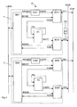
- an apparatus 10 comprising two units 1 and 2 have been disclosed.
- Each unit comprises a clock functionality and additional functionality (not shown).
- the clock functionality of the two units are identical and are coupled to one another over a clock bus, comprising a system clock line, SCLK, and an internal clock line, ICLK, and over a logic bus, L-BUS.
- the additional functionality could relate to virtually any functionality requiring a clock signal, such as telecom radio base station functionality.
- the additional functionality of the units may not necessarily be the same.
- the units could be arranged on separate circuit boards fitting in a common rack.
- three or more units could be coupled to the above-mentioned busses; whereby a given unit is master and the other units are slaves.
- the system clock SCLK is the clock reference signal provided to all units from the given dedicated master unit.
- the first unit comprises a logic section MS1, a clock source CLK1, comprising for instance a quartz clock, a phase lock loop (PLL) device P1, a first bi-directional port BD11 and a second bi-directional port BD12.
- a logic section MS1 a clock source CLK1 comprising for instance a quartz clock
- a phase lock loop (PLL) device P1 comprising for instance a quartz clock
- PLL phase lock loop
- the clock source CLK1 is generating a clock source signal CLK10, which may be halted upon reception of an asynchronous command signal ASCMD1.
- the clock source signal CLK10 is issued to the first bi-directional port BD11.
- BD11 Depending on the state of an enable signal BD11E, BD11 has the following function: If enabled, BD11 outputs the source clock signal CLK10 to the internal clock ICLK over a line B11 and concurrently imports the same clock signal. If disabled, BD11 imports a clock signal from the internal clock ICLK over a line B11
- the first bi-directional port BD11 transfers the occurring source signal on line B11 into line CLKB1 to phased lock loop (PLL) device P1.
- PLL phased lock loop
- a PLL device will, if exposed to a periodical input signal, provide the same signal on its output. However, should a single pulse alter in the input signal or should the frequency of the input signal alter stepwise, the PLL will - in analogy to a gyro system - slowly change its output such that the output gradually will match the frequency and phase of the incoming signal.
- the PLL device contains an internal feedback loop illustrated by line P1 L.
- the PLL device P1 produces a derived clock signal CLKP1 that is input to second bi-directional port BD12.
- BD12 Depending on the state of an enable signal BD12E, BD12 has the following function: If enabled, BD12 outputs the source clock signal CLKP1 to the system clock SCLK over a line B12 and concurrently imports the same clock signal. If disabled, BD12 imports a clock signal from the system clock SCLK over a line B12 and passes it further on as a signal CLKL1.
- the derived clock signal present on system clock SCLK is lead to logic section MS1.
- Both enable signals BD11 E and BD12E is output from logic signal MS1.
- the second unit 2 is identical to unit 1, although the reference numerals of unit 2 are different for the same type of elements found in unit 1.
- operation is so that one unit is master while the remaining units are slaves.
- the master unit controls the system clock SCLK and the internal clock ICLK, while the slave units sense the former two clock signals.
- the change of master from one unit to another is accomplished according to the operation of logic sections MS1 and MS2.
- the operation enables switching according to sensed error states but also enables intended master changeovers, which are not caused by faults.
- the dedication of master unit is dependent on a signal being given on the L-bus so as not to select a given unit for being a master unit, and if a given unit is dedicated as master unit when such a signal on the L-bus is given, the system performs a switchover causing another unit as the one not selected to be dedicated as master unit.
- the changeover could be effectuated by an external asynchronous signal, such as the one given when an operator prepares for a hot swap and for instance gives a command signal ASCMD1.
- the logic section of a given unit is synchronised with the system clock SCLK over the signal lines CLKL1, CLKL2.
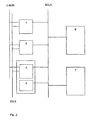
- FIG. 2 another exemplary coupling scheme according to the invention has been shown comprising three redundant clock units 1, 2 and 3 on separate boards and two boards 6, 7 with additional functionality but without any clock generating or clock evaluating functionality. All boards are connected over the system clock line SCLK. The clock unit 3 and additional functionality 5 reside on the same board. The clock units are moreover interconnected by the L-BUS and the internal clock line ICLK.
- the two clock sources CLK1 and CLK2 produce two signals CLK10 and CLK20 of substantially the same frequency but which are lagging in phase to one another with an arbitrary phase difference that could amount to +/- 180 degrees.
- a signal indicative of an intended change in master from unit 1 to unit 2 is signalled on the L-BUS.
- all enable signals BD11E, BD12E, BD21E and BD22E changes states at T4. This effects the change of master from unit 1 to unit 2.
- the internal clock signal ICLK is given by the source clock chosen, corresponding to the selected master. Before T5, the internal clock is following CLK10 and after T5, the internal clock follows CLK20, as signalled over BD11E and BD21 E.
- a phase shift in ICLK occurs at T5 as switchover is made between CLK10 and CLK20.
- the signalling from the logic sections MS1 and MS2 secures that at all times the signals CLKB1, CLKB2 are fetched from the same clock source.
- the internal clock ICLK always depends on the one selected internal clock. Consequently, the inputs to the various PLL's are identical. All PLL's have the same predetermined characteristic and the tolerance level applicable for the PLL units are chosen to be appropriately small.
- the various outputs of the PLL's - CLKP1 and CLKP2 - will always be substantially in phase and be dependent on the prevalent dedicated internal clock signal ICLK. Therefore, the system clock SCLK can be switched over virtually seamlessly from CLKP1 to CLKP2 and vice versa as controlled by logic signals BD12E and BD22E.
- the PLL's P1 and P2 will maintain generating phase aligned clock signals CLKP1 and CLKP2 for several clock cycles, even if no internal clock ICLK signal is present.
- the PLL's When the ICLK signal changes abruptly from a first phase value to a second phase value - as illustrated at T5 - the PLL's will gradually change the phase of their outputs so that after a given period - at T6 - the PLL's will be in phase with the second phase value of the ICLK signal.
- the inertia of the PLL's and the corresponding period of "ramp alignment" is chosen to match the system clock requirements of the additional functionality mentioned above.
- the phase change is off course associated with a change in clock cycle frequency.
- the frequency FSC of the system clock signal SCLK has been illustrated as changing from a first frequency F1 at time T1 to a second frequency F2 immediately after T5.
- the frequency FSC approaches asymptotically the first frequency F1.
- the alignment period T5 - T6 is chosen to several clock cycles, such that the additional functionality "won't notice" the phase change.
- the phase difference is illustrated as being insignificant.
- the enable signals BD11 E, BD12E, BD21 E and BD22E are related to the first positive edge of SCLK that is overlapped by the L-bus signal. Thereby the state changes of enable signals occur following a positive edge of SCLK.
- the short delay from SCLK going high at T3 to the enable signals are changing state at T4 is due to propagation delays in the circuitry.
- the switching of output enable signals is first accomplished when it is known that SCLK is in a logic high state at a time with a certain predetermined security time interval from state changes, i.e. at a certain distance to the flanks. It is important that the switch does not occur when there is a transition of SCLK, since this could cause disturbances at the receiver end.
- an external circuitry is used to bias the SCLK line to a logic high state, in case no unit should drive the SCLK line. Since switching can only occur when SCLK is high, there is thus no possibility that no unit is driving the SCLK line for a short moment when one unit is turning off and the other is turning on.
- the external circuitry comprises a pull-up resistor R1 being arranged between a system high voltage Vcc and the system SCLK.
- the means for providing error detection and the methods for obtaining appropriate fault management routines can be implemented in a variety of ways.
- the logic sections MS of each unit comprises functionality to notify other units about whether the given unit is connected (or possibly suffers a fail state) to the I-CLK and the S-CLK line or not.
- Each logic unit moreover comprises functionality to learn about which other units are connected.
- a priority scheme is negotiated every time there is a change in the units being connected, involving that a priority scheme according to which a predetermined order for dedicating units is determined. Thereby, all units agree on a subsequent master is being dedicated in case another master suffers a fail state.
- the priority scheme could for instance be arranged according to the order at which modules are connected. A random order could also be envisioned.
- the logic sections constitute an autonomous control of the clock system disregarding the actual number of clock units being present. No superior or additional clock circuitry is needed.
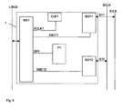
- Fig. 4 shows a preferred embodiment of fault sense circuitry in the first unit shown in fig. 1 .
- the operation of clock source CLK1 is provided with error status line SCLK1 that can be checked by the logic section MS1 reading the state of SCLK1.
- the error status of bi-directional port BD11 is read over SBD11
- the error status of bi-directional port BD12 is read over SBD12
- the error status of PLL device P1 is read over SP1.
- the reliability of PLL devices and the bi-directional unit coupled to the output of the PLL device is of a high standard.
- the master unit is not necessarily outputting the clock source on the internal clock line while controlling the system clock line at the same time.
- a given unit could be master for the system clock, while another unit could be master for the internal clock line.
- the logic circuitry could effectuate that in case more than two units are prevalent, a mastership for the system clock line is dedicated to a first unit while the mastership for the internal clock line is dedicated to another units.
Landscapes
- Engineering & Computer Science (AREA)
- Theoretical Computer Science (AREA)
- Physics & Mathematics (AREA)
- General Engineering & Computer Science (AREA)
- General Physics & Mathematics (AREA)
- Quality & Reliability (AREA)
- Synchronisation In Digital Transmission Systems (AREA)
- Electronic Switches (AREA)
- Stabilization Of Oscillater, Synchronisation, Frequency Synthesizers (AREA)
- Saccharide Compounds (AREA)
- Manipulation Of Pulses (AREA)
Claims (7)
- Unité (1, 2, 3) comprenant :une source d'horloge (CLK1, CLK2) pour générer un signal de source d'horloge (CLK10, CLK20),un premier port (BD11, BD21) pour communiquer avec une ligne d'horloge interne (ICLK) et un deuxième port (BD12, BD22) pour communiquer avec une ligne d'horloge de système (SCLK),un dispositif de boucle à verrouillage de phase (P1, P2) ayant une caractéristique prédéterminée et pour générer un signal d'horloge (CLKP1),une section logique (MS) pour communiquer avec un bus logique (L-BUS), la section logique déterminant si l'unité est dédiée en tant qu'unité maître ou esclave, caractérisée en ce quele dispositif de boucle à verrouillage de phase (P1, P2) génère un signal d'horloge (CLKP1, CLKP2), qui est déduit d'un signal d'horloge sur la ligne d'horloge interne (ICLK) ou de la source d'horloge dans l'unité,le premier port (BD11 ; BD21) étant bidirectionnel pour délivrer le signal de source d'horloge à la ligne d'horloge interne (ICLK) ou appliquer un signal d'horloge interne provenant de la ligne d'horloge interne au dispositif de boucle à verrouillage de phase (P1, P2),le deuxième port (BD12 ; BD22) étant bidirectionnel pour délivrer le signal d'horloge provenant du dispositif de boucle à verrouillage de phase (P1, P2) à la ligne d'horloge de système (SCLK) ou appliquer le signal d'horloge provenant de la ligne d'horloge de système à la section logique (MS1, MS2),la section logique (MS) commande les premier et deuxième ports bidirectionnels (BD11, BD12, BD21, BD22) par l'intermédiaire de signaux de validation (BD11E, BD12E, BD21E, BD22E), moyennant quoi la section logique (MS) lorsqu'il est déterminé que l'unité est dédiée en tant qu'unité maître,- commande le signal d'horloge de source (CLK110, CLK20) pour qu'il soit délivré sur la ligne d'horloge interne (ICLK) et/ou- commande le signal génère par la boucle à verrouillage de phase déduit du signal d'horloge de la ligne d'horloge interne pour qu'il soit sur la ligne d'horloge de système (SCLK).
- Unité selon la revendication 1, dans laquelle les signaux de validation (BD12E, promenant de la section logique (MS) changent en premier d'état lorsque le signal d'horloge de la ligne d'horloge de système (SCLK) est dans un état logique avec un certain intervalle de sécurité prédéterminé par rapport aux changements d'état du signal d'horloge de la ligne d'horloge de système (SCLK).
- Système (10) comprenant au moins deux unités (1, 2, 3) selon quelconque des revendications 1 ou 2, les unités étant couplées à une ligne d'horloge de système (SCLK) commune, une ligne d'horloge interne (ICLK) commune et un bus logique (L-BUS), moyennant quoi une seule unité (1, 2) est dédiée en tant qu'unité maître à un instant donné.
- Système selon la revendications 3, par lequel la section logique (MS), en coopération avec d'autres sections logiques d'autres unités, négocie une méthode de priorité selon laquelle un ordre prédéterminé pour dédier les unités en tant qu'unités maîtres est déterminé.
- Système selon l'une quelconque des revendications 2 à 4, dans lequel la section logique d'une quelconque unité comprend des éléments de circuit de détection de défaut, et par lequel, si un défaut est détecté dans un quelconque dispositif, le système lance une commutation d'une unité dédiée à une unité dédiée suivante.
- Système selon l'une quelconque des revendications 2 à 5, comprenant une carte supplémentaire (6, 7) ne comprenant pas de fonctionnalité de génération d'horloge ou d'évaluation d'horloge, la carte supplémentaire étant couplée à la ligne d'horloge de système (SCLK) mais pas à la ligne d'horloge interne (ICLK) ni au bus logique (L-BUS),
- Système selon l'une quelconque des revendications 2 à 6, comprenant au moins trois unités (1, 2, 3).
Applications Claiming Priority (1)
| Application Number | Priority Date | Filing Date | Title |
|---|---|---|---|
| PCT/SE2002/000252 WO2003069451A1 (fr) | 2002-02-14 | 2002-02-14 | Signaux d'horloge continus |
Publications (2)
| Publication Number | Publication Date |
|---|---|
| EP1476800A1 EP1476800A1 (fr) | 2004-11-17 |
| EP1476800B1 true EP1476800B1 (fr) | 2010-11-17 |
Family
ID=27731061
Family Applications (1)
| Application Number | Title | Priority Date | Filing Date |
|---|---|---|---|
| EP02711610A Expired - Lifetime EP1476800B1 (fr) | 2002-02-14 | 2002-02-14 | Signaux d'horloge continus |
Country Status (9)
| Country | Link |
|---|---|
| US (1) | US7386079B2 (fr) |
| EP (1) | EP1476800B1 (fr) |
| JP (1) | JP4061273B2 (fr) |
| KR (1) | KR100882391B1 (fr) |
| AT (1) | ATE488796T1 (fr) |
| AU (1) | AU2002230357A1 (fr) |
| DE (1) | DE60238353D1 (fr) |
| ES (1) | ES2354195T3 (fr) |
| WO (1) | WO2003069451A1 (fr) |
Families Citing this family (15)
| Publication number | Priority date | Publication date | Assignee | Title |
|---|---|---|---|---|
| US7117086B2 (en) * | 2003-09-08 | 2006-10-03 | Honeywell International Inc. | GPS/IMU clock synchronization particularly for deep integration vector tracking loop |
| CN1305326C (zh) * | 2003-11-04 | 2007-03-14 | 上海贝尔阿尔卡特股份有限公司 | 为无线网络控制器产生和分配内部时钟的方法及装置 |
| TWI277302B (en) * | 2004-12-28 | 2007-03-21 | Ind Tech Res Inst | Clock and data recovery circuit |
| US7555670B2 (en) * | 2005-10-26 | 2009-06-30 | Intel Corporation | Clocking architecture using a bidirectional clock port |
| US8121209B2 (en) | 2006-07-25 | 2012-02-21 | Marvell World Trade Ltd. | Concatenation-assisted symbol-level combining for MIMO systems with HARQ and/or repetition coding |
| US8929472B1 (en) | 2006-07-26 | 2015-01-06 | Marvell International Ltd. | Bit-level combining for MIMO systems with HARQ and/or repetition coding |
| US8718166B2 (en) * | 2006-08-08 | 2014-05-06 | Marvell World Trade Ltd. | Maximal ratio combining of equalized symbols for MIMO systems with HARQ and/or repetition coding |
| US8699601B1 (en) | 2006-08-08 | 2014-04-15 | Marvell World Trade Ltd. | Distance-level combining for MIMO systems with HARQ and/or repetition coding |
| US8411778B1 (en) | 2006-08-08 | 2013-04-02 | Marvell World Trade Ltd. | Optimal linear equalizer for MIMO systems with HARQ and/or repetition coding |
| US7809025B2 (en) * | 2006-09-29 | 2010-10-05 | Hewlett-Packard Development Company, L.P. | System and method for distributing clock signals |
| US8619910B1 (en) * | 2007-04-11 | 2013-12-31 | Marvell International Ltd. | Decision feedback equalization for MIMO systems with hybrid ARQ |
| US7840190B2 (en) * | 2007-07-26 | 2010-11-23 | Mobile Access Networks Ltd. | Frequency source synchronization and redundancy |
| GB2497314A (en) * | 2011-12-06 | 2013-06-12 | St Microelectronics Grenoble 2 | Independent blocks to control independent busses or a single combined bus |
| US20150033050A1 (en) * | 2013-07-25 | 2015-01-29 | Samsung Electronics Co., Ltd | Semiconductor integrated circuit and computing device including the same |
| WO2015063758A1 (fr) | 2013-10-28 | 2015-05-07 | Corning Optical Communications Wireless Ltd. | Systèmes d'antennes distribuées (das) unifiés à base de fibres optiques pour la prise en charge du déploiement de communications par petites cellules depuis de multiples fournisseurs de services par petites cellules, et dispositifs et procédés associés |
Citations (1)
| Publication number | Priority date | Publication date | Assignee | Title |
|---|---|---|---|---|
| US5852728A (en) * | 1995-01-12 | 1998-12-22 | Hitachi, Ltd. | Uninterruptible clock supply apparatus for fault tolerant computer system |
Family Cites Families (16)
| Publication number | Priority date | Publication date | Assignee | Title |
|---|---|---|---|---|
| US4282493A (en) * | 1979-07-02 | 1981-08-04 | Motorola, Inc. | Redundant clock signal generating circuitry |
| US5133064A (en) * | 1987-04-27 | 1992-07-21 | Hitachi, Ltd. | Data processing system generating clock signal from an input clock, phase locked to the input clock and used for clocking logic devices |
| JPH0779336B2 (ja) * | 1989-05-22 | 1995-08-23 | パイオニア株式会社 | 双方向通信ラインのバッファ装置 |
| US5124569A (en) * | 1990-10-18 | 1992-06-23 | Star Technologies, Inc. | Digital phase-lock loop system with analog voltage controlled oscillator |
| US5577075A (en) * | 1991-09-26 | 1996-11-19 | Ipc Information Systems, Inc. | Distributed clocking system |
| US5826093A (en) * | 1994-12-22 | 1998-10-20 | Adaptec, Inc. | Dual function disk drive integrated circuit for master mode and slave mode operations |
| US6247138B1 (en) * | 1997-06-12 | 2001-06-12 | Fujitsu Limited | Timing signal generating circuit, semiconductor integrated circuit device and semiconductor integrated circuit system to which the timing signal generating circuit is applied, and signal transmission system |
| US5889435A (en) * | 1997-06-30 | 1999-03-30 | Sun Microsystems, Inc. | On-chip PLL phase and jitter self-test circuit |
| US6078192A (en) * | 1997-09-18 | 2000-06-20 | Ericsson, Inc. | Circuit and method for using the I2 C serial protocol with multiple voltages |
| US6359945B1 (en) * | 1999-01-25 | 2002-03-19 | Sun Microsystems, Inc. | Phase locked loop and method that provide fail-over redundant clocking |
| US6194969B1 (en) * | 1999-05-19 | 2001-02-27 | Sun Microsystems, Inc. | System and method for providing master and slave phase-aligned clocks |
| JP2001021624A (ja) * | 1999-07-07 | 2001-01-26 | Fujitsu Ltd | テストデータ生成システム及び方法並びにテストデータ生成プログラムを記録した記録媒体 |
| US6754745B1 (en) * | 1999-08-06 | 2004-06-22 | Accelerated Networks | Method and apparatus for distributing a clock in a network |
| SE517967C2 (sv) | 2000-03-23 | 2002-08-06 | Ericsson Telefon Ab L M | System och förfarande för klocksignalgenerering |
| EP1139611A2 (fr) | 2000-03-31 | 2001-10-04 | Alcatel USA Sourcing, L.P. | Module de contrôle de bus |
| US7180821B2 (en) * | 2004-09-30 | 2007-02-20 | Infineon Technologies Ag | Memory device, memory controller and memory system having bidirectional clock lines |
-
2002
- 2002-02-14 EP EP02711610A patent/EP1476800B1/fr not_active Expired - Lifetime
- 2002-02-14 DE DE60238353T patent/DE60238353D1/de not_active Expired - Lifetime
- 2002-02-14 ES ES02711610T patent/ES2354195T3/es not_active Expired - Lifetime
- 2002-02-14 US US10/502,422 patent/US7386079B2/en not_active Expired - Fee Related
- 2002-02-14 WO PCT/SE2002/000252 patent/WO2003069451A1/fr active Application Filing
- 2002-02-14 AT AT02711610T patent/ATE488796T1/de not_active IP Right Cessation
- 2002-02-14 AU AU2002230357A patent/AU2002230357A1/en not_active Abandoned
- 2002-02-14 KR KR1020047012495A patent/KR100882391B1/ko active IP Right Grant
- 2002-02-14 JP JP2003568509A patent/JP4061273B2/ja not_active Expired - Fee Related
Patent Citations (1)
| Publication number | Priority date | Publication date | Assignee | Title |
|---|---|---|---|---|
| US5852728A (en) * | 1995-01-12 | 1998-12-22 | Hitachi, Ltd. | Uninterruptible clock supply apparatus for fault tolerant computer system |
Also Published As
| Publication number | Publication date |
|---|---|
| JP2005518012A (ja) | 2005-06-16 |
| ATE488796T1 (de) | 2010-12-15 |
| WO2003069451A1 (fr) | 2003-08-21 |
| US20050123085A1 (en) | 2005-06-09 |
| EP1476800A1 (fr) | 2004-11-17 |
| KR100882391B1 (ko) | 2009-02-05 |
| JP4061273B2 (ja) | 2008-03-12 |
| AU2002230357A1 (en) | 2003-09-04 |
| ES2354195T3 (es) | 2011-03-10 |
| KR20040089624A (ko) | 2004-10-21 |
| US7386079B2 (en) | 2008-06-10 |
| DE60238353D1 (de) | 2010-12-30 |
| ES2354195T8 (es) | 2011-05-03 |
Similar Documents
| Publication | Publication Date | Title |
|---|---|---|
| EP1476800B1 (fr) | Signaux d'horloge continus | |
| US6194969B1 (en) | System and method for providing master and slave phase-aligned clocks | |
| US7089442B2 (en) | Fault-tolerant clock generator | |
| US5146585A (en) | Synchronized fault tolerant clocks for multiprocessor systems | |
| US7308592B2 (en) | Redundant oscillator distribution in a multi-processor server system | |
| US7239681B2 (en) | System and method for maintaining a stable synchronization state in a programmable clock synchronizer | |
| EP0280258B1 (fr) | Dispositif de commande de temps tolérant des fautes | |
| US5594896A (en) | Method for switching between a plurality of clock sources upon detection of phase alignment thereof and disabling all other clock sources | |
| WO2001052417A2 (fr) | Systeme et procede de boucle a phase asservie | |
| US6675307B1 (en) | Clock controller for controlling the switching to redundant clock signal without producing glitches by delaying the redundant clock signal to match a phase of primary clock signal | |
| US5381416A (en) | Detection of skew fault in a multiple clock system | |
| WO2012081196A1 (fr) | Circuit de sélection de signal et procédé de sélection de signal | |
| US20040223564A1 (en) | Programmable clock synchronizer | |
| JPH033419A (ja) | 位相同期回路 | |
| JP2602421B2 (ja) | クロック受信分配システム | |
| US5859996A (en) | Clock signal supply for fault tolerant data processing | |
| JP2978884B1 (ja) | クロック交絡分配装置 | |
| JPH02168308A (ja) | クロック信号供給装置 | |
| JP2645880B2 (ja) | システムクロック二重化方式 | |
| JP3327018B2 (ja) | クロック供給装置 | |
| JPH06232739A (ja) | クロック冗長化方式 | |
| JPH04267652A (ja) | クロック位相同期システム | |
| JPS6255717A (ja) | 共通クロツク信号供給方式 | |
| JPH07255097A (ja) | クロック切り換え装置およびその方法 | |
| JPH1028037A (ja) | クロック切替回路 |
Legal Events
| Date | Code | Title | Description |
|---|---|---|---|
| PUAI | Public reference made under article 153(3) epc to a published international application that has entered the european phase |
Free format text: ORIGINAL CODE: 0009012 |
|
| 17P | Request for examination filed |
Effective date: 20040914 |
|
| AK | Designated contracting states |
Kind code of ref document: A1 Designated state(s): AT BE CH CY DE DK ES FI FR GB GR IE IT LI LU MC NL PT SE TR |
|
| AX | Request for extension of the european patent |
Extension state: AL LT LV MK RO SI |
|
| RIN1 | Information on inventor provided before grant (corrected) |
Inventor name: SKOG, LARS Inventor name: LEGNEDAHL, NIKLAS |
|
| 17Q | First examination report despatched |
Effective date: 20060515 |
|
| GRAP | Despatch of communication of intention to grant a patent |
Free format text: ORIGINAL CODE: EPIDOSNIGR1 |
|
| GRAS | Grant fee paid |
Free format text: ORIGINAL CODE: EPIDOSNIGR3 |
|
| GRAA | (expected) grant |
Free format text: ORIGINAL CODE: 0009210 |
|
| AK | Designated contracting states |
Kind code of ref document: B1 Designated state(s): AT BE CH CY DE DK ES FI FR GB GR IE IT LI LU MC NL PT SE TR |
|
| REG | Reference to a national code |
Ref country code: GB Ref legal event code: FG4D |
|
| REG | Reference to a national code |
Ref country code: CH Ref legal event code: EP |
|
| REG | Reference to a national code |
Ref country code: IE Ref legal event code: FG4D |
|
| REF | Corresponds to: |
Ref document number: 60238353 Country of ref document: DE Date of ref document: 20101230 Kind code of ref document: P |
|
| REG | Reference to a national code |
Ref country code: NL Ref legal event code: VDEP Effective date: 20101117 |
|
| REG | Reference to a national code |
Ref country code: ES Ref legal event code: FG2A Effective date: 20110228 |
|
| PG25 | Lapsed in a contracting state [announced via postgrant information from national office to epo] |
Ref country code: NL Free format text: LAPSE BECAUSE OF FAILURE TO SUBMIT A TRANSLATION OF THE DESCRIPTION OR TO PAY THE FEE WITHIN THE PRESCRIBED TIME-LIMIT Effective date: 20101117 Ref country code: SE Free format text: LAPSE BECAUSE OF FAILURE TO SUBMIT A TRANSLATION OF THE DESCRIPTION OR TO PAY THE FEE WITHIN THE PRESCRIBED TIME-LIMIT Effective date: 20101117 Ref country code: CY Free format text: LAPSE BECAUSE OF FAILURE TO SUBMIT A TRANSLATION OF THE DESCRIPTION OR TO PAY THE FEE WITHIN THE PRESCRIBED TIME-LIMIT Effective date: 20101117 Ref country code: PT Free format text: LAPSE BECAUSE OF FAILURE TO SUBMIT A TRANSLATION OF THE DESCRIPTION OR TO PAY THE FEE WITHIN THE PRESCRIBED TIME-LIMIT Effective date: 20110317 Ref country code: FI Free format text: LAPSE BECAUSE OF FAILURE TO SUBMIT A TRANSLATION OF THE DESCRIPTION OR TO PAY THE FEE WITHIN THE PRESCRIBED TIME-LIMIT Effective date: 20101117 Ref country code: AT Free format text: LAPSE BECAUSE OF FAILURE TO SUBMIT A TRANSLATION OF THE DESCRIPTION OR TO PAY THE FEE WITHIN THE PRESCRIBED TIME-LIMIT Effective date: 20101117 |
|
| PG25 | Lapsed in a contracting state [announced via postgrant information from national office to epo] |
Ref country code: GR Free format text: LAPSE BECAUSE OF FAILURE TO SUBMIT A TRANSLATION OF THE DESCRIPTION OR TO PAY THE FEE WITHIN THE PRESCRIBED TIME-LIMIT Effective date: 20110218 |
|
| PG25 | Lapsed in a contracting state [announced via postgrant information from national office to epo] |
Ref country code: BE Free format text: LAPSE BECAUSE OF FAILURE TO SUBMIT A TRANSLATION OF THE DESCRIPTION OR TO PAY THE FEE WITHIN THE PRESCRIBED TIME-LIMIT Effective date: 20101117 |
|
| PG25 | Lapsed in a contracting state [announced via postgrant information from national office to epo] |
Ref country code: DK Free format text: LAPSE BECAUSE OF FAILURE TO SUBMIT A TRANSLATION OF THE DESCRIPTION OR TO PAY THE FEE WITHIN THE PRESCRIBED TIME-LIMIT Effective date: 20101117 |
|
| PLBE | No opposition filed within time limit |
Free format text: ORIGINAL CODE: 0009261 |
|
| STAA | Information on the status of an ep patent application or granted ep patent |
Free format text: STATUS: NO OPPOSITION FILED WITHIN TIME LIMIT |
|
| PG25 | Lapsed in a contracting state [announced via postgrant information from national office to epo] |
Ref country code: MC Free format text: LAPSE BECAUSE OF NON-PAYMENT OF DUE FEES Effective date: 20110228 |
|
| REG | Reference to a national code |
Ref country code: CH Ref legal event code: PL |
|
| 26N | No opposition filed |
Effective date: 20110818 |
|
| PG25 | Lapsed in a contracting state [announced via postgrant information from national office to epo] |
Ref country code: CH Free format text: LAPSE BECAUSE OF NON-PAYMENT OF DUE FEES Effective date: 20110228 Ref country code: LI Free format text: LAPSE BECAUSE OF NON-PAYMENT OF DUE FEES Effective date: 20110228 |
|
| REG | Reference to a national code |
Ref country code: FR Ref legal event code: ST Effective date: 20111102 |
|
| REG | Reference to a national code |
Ref country code: IE Ref legal event code: MM4A |
|
| REG | Reference to a national code |
Ref country code: DE Ref legal event code: R097 Ref document number: 60238353 Country of ref document: DE Effective date: 20110818 |
|
| PG25 | Lapsed in a contracting state [announced via postgrant information from national office to epo] |
Ref country code: IT Free format text: LAPSE BECAUSE OF FAILURE TO SUBMIT A TRANSLATION OF THE DESCRIPTION OR TO PAY THE FEE WITHIN THE PRESCRIBED TIME-LIMIT Effective date: 20101117 |
|
| PG25 | Lapsed in a contracting state [announced via postgrant information from national office to epo] |
Ref country code: FR Free format text: LAPSE BECAUSE OF NON-PAYMENT OF DUE FEES Effective date: 20110228 Ref country code: IE Free format text: LAPSE BECAUSE OF NON-PAYMENT OF DUE FEES Effective date: 20110214 |
|
| PG25 | Lapsed in a contracting state [announced via postgrant information from national office to epo] |
Ref country code: LU Free format text: LAPSE BECAUSE OF NON-PAYMENT OF DUE FEES Effective date: 20110214 |
|
| PG25 | Lapsed in a contracting state [announced via postgrant information from national office to epo] |
Ref country code: TR Free format text: LAPSE BECAUSE OF FAILURE TO SUBMIT A TRANSLATION OF THE DESCRIPTION OR TO PAY THE FEE WITHIN THE PRESCRIBED TIME-LIMIT Effective date: 20101117 |
|
| PGFP | Annual fee paid to national office [announced via postgrant information from national office to epo] |
Ref country code: ES Payment date: 20160226 Year of fee payment: 15 Ref country code: DE Payment date: 20160226 Year of fee payment: 15 |
|
| PGFP | Annual fee paid to national office [announced via postgrant information from national office to epo] |
Ref country code: GB Payment date: 20160226 Year of fee payment: 15 |
|
| REG | Reference to a national code |
Ref country code: DE Ref legal event code: R119 Ref document number: 60238353 Country of ref document: DE |
|
| GBPC | Gb: european patent ceased through non-payment of renewal fee |
Effective date: 20170214 |
|
| PG25 | Lapsed in a contracting state [announced via postgrant information from national office to epo] |
Ref country code: DE Free format text: LAPSE BECAUSE OF NON-PAYMENT OF DUE FEES Effective date: 20170901 |
|
| PG25 | Lapsed in a contracting state [announced via postgrant information from national office to epo] |
Ref country code: GB Free format text: LAPSE BECAUSE OF NON-PAYMENT OF DUE FEES Effective date: 20170214 |
|
| REG | Reference to a national code |
Ref country code: ES Ref legal event code: FD2A Effective date: 20180704 |
|
| PG25 | Lapsed in a contracting state [announced via postgrant information from national office to epo] |
Ref country code: ES Free format text: LAPSE BECAUSE OF NON-PAYMENT OF DUE FEES Effective date: 20170215 |