EP1450345A2 - Anzeigevorrichtung mit aktiver Matrix und Steuerverfahren dafür - Google Patents
Anzeigevorrichtung mit aktiver Matrix und Steuerverfahren dafür Download PDFInfo
- Publication number
- EP1450345A2 EP1450345A2 EP04003140A EP04003140A EP1450345A2 EP 1450345 A2 EP1450345 A2 EP 1450345A2 EP 04003140 A EP04003140 A EP 04003140A EP 04003140 A EP04003140 A EP 04003140A EP 1450345 A2 EP1450345 A2 EP 1450345A2
- Authority
- EP
- European Patent Office
- Prior art keywords
- light emitting
- emitting display
- measuring
- display device
- drive
- Prior art date
- Legal status (The legal status is an assumption and is not a legal conclusion. Google has not performed a legal analysis and makes no representation as to the accuracy of the status listed.)
- Withdrawn
Links
Images


Classifications
-
- G—PHYSICS
- G09—EDUCATION; CRYPTOGRAPHY; DISPLAY; ADVERTISING; SEALS
- G09G—ARRANGEMENTS OR CIRCUITS FOR CONTROL OF INDICATING DEVICES USING STATIC MEANS TO PRESENT VARIABLE INFORMATION
- G09G3/00—Control arrangements or circuits, of interest only in connection with visual indicators other than cathode-ray tubes
- G09G3/20—Control arrangements or circuits, of interest only in connection with visual indicators other than cathode-ray tubes for presentation of an assembly of a number of characters, e.g. a page, by composing the assembly by combination of individual elements arranged in a matrix no fixed position being assigned to or needed to be assigned to the individual characters or partial characters
- G09G3/22—Control arrangements or circuits, of interest only in connection with visual indicators other than cathode-ray tubes for presentation of an assembly of a number of characters, e.g. a page, by composing the assembly by combination of individual elements arranged in a matrix no fixed position being assigned to or needed to be assigned to the individual characters or partial characters using controlled light sources
- G09G3/30—Control arrangements or circuits, of interest only in connection with visual indicators other than cathode-ray tubes for presentation of an assembly of a number of characters, e.g. a page, by composing the assembly by combination of individual elements arranged in a matrix no fixed position being assigned to or needed to be assigned to the individual characters or partial characters using controlled light sources using electroluminescent panels
- G09G3/32—Control arrangements or circuits, of interest only in connection with visual indicators other than cathode-ray tubes for presentation of an assembly of a number of characters, e.g. a page, by composing the assembly by combination of individual elements arranged in a matrix no fixed position being assigned to or needed to be assigned to the individual characters or partial characters using controlled light sources using electroluminescent panels semiconductive, e.g. using light-emitting diodes [LED]
- G09G3/3208—Control arrangements or circuits, of interest only in connection with visual indicators other than cathode-ray tubes for presentation of an assembly of a number of characters, e.g. a page, by composing the assembly by combination of individual elements arranged in a matrix no fixed position being assigned to or needed to be assigned to the individual characters or partial characters using controlled light sources using electroluminescent panels semiconductive, e.g. using light-emitting diodes [LED] organic, e.g. using organic light-emitting diodes [OLED]
- G09G3/3225—Control arrangements or circuits, of interest only in connection with visual indicators other than cathode-ray tubes for presentation of an assembly of a number of characters, e.g. a page, by composing the assembly by combination of individual elements arranged in a matrix no fixed position being assigned to or needed to be assigned to the individual characters or partial characters using controlled light sources using electroluminescent panels semiconductive, e.g. using light-emitting diodes [LED] organic, e.g. using organic light-emitting diodes [OLED] using an active matrix
- G09G3/3258—Control arrangements or circuits, of interest only in connection with visual indicators other than cathode-ray tubes for presentation of an assembly of a number of characters, e.g. a page, by composing the assembly by combination of individual elements arranged in a matrix no fixed position being assigned to or needed to be assigned to the individual characters or partial characters using controlled light sources using electroluminescent panels semiconductive, e.g. using light-emitting diodes [LED] organic, e.g. using organic light-emitting diodes [OLED] using an active matrix with pixel circuitry controlling the voltage across the light-emitting element
-
- G—PHYSICS
- G09—EDUCATION; CRYPTOGRAPHY; DISPLAY; ADVERTISING; SEALS
- G09G—ARRANGEMENTS OR CIRCUITS FOR CONTROL OF INDICATING DEVICES USING STATIC MEANS TO PRESENT VARIABLE INFORMATION
- G09G2300/00—Aspects of the constitution of display devices
- G09G2300/08—Active matrix structure, i.e. with use of active elements, inclusive of non-linear two terminal elements, in the pixels together with light emitting or modulating elements
- G09G2300/0809—Several active elements per pixel in active matrix panels
- G09G2300/0842—Several active elements per pixel in active matrix panels forming a memory circuit, e.g. a dynamic memory with one capacitor
-
- G—PHYSICS
- G09—EDUCATION; CRYPTOGRAPHY; DISPLAY; ADVERTISING; SEALS
- G09G—ARRANGEMENTS OR CIRCUITS FOR CONTROL OF INDICATING DEVICES USING STATIC MEANS TO PRESENT VARIABLE INFORMATION
- G09G2320/00—Control of display operating conditions
- G09G2320/02—Improving the quality of display appearance
- G09G2320/029—Improving the quality of display appearance by monitoring one or more pixels in the display panel, e.g. by monitoring a fixed reference pixel
-
- G—PHYSICS
- G09—EDUCATION; CRYPTOGRAPHY; DISPLAY; ADVERTISING; SEALS
- G09G—ARRANGEMENTS OR CIRCUITS FOR CONTROL OF INDICATING DEVICES USING STATIC MEANS TO PRESENT VARIABLE INFORMATION
- G09G2320/00—Control of display operating conditions
- G09G2320/04—Maintaining the quality of display appearance
- G09G2320/043—Preventing or counteracting the effects of ageing
- G09G2320/045—Compensation of drifts in the characteristics of light emitting or modulating elements
-
- G—PHYSICS
- G09—EDUCATION; CRYPTOGRAPHY; DISPLAY; ADVERTISING; SEALS
- G09G—ARRANGEMENTS OR CIRCUITS FOR CONTROL OF INDICATING DEVICES USING STATIC MEANS TO PRESENT VARIABLE INFORMATION
- G09G2330/00—Aspects of power supply; Aspects of display protection and defect management
- G09G2330/02—Details of power systems and of start or stop of display operation
- G09G2330/028—Generation of voltages supplied to electrode drivers in a matrix display other than LCD
Definitions
- the present invention relates to an active drive type light emitting display device provided with measuring pixels in addition to light emitting display pixels, and particularly to a light emitting display device and a drive control method thereof in which the light emitting display pixels can be efficiently driven by obtaining forward voltages of light emitting elements by means of the measuring pixels.
- a display using a display panel which is constructed by arranging light emitting elements in a matrix pattern has been developed widely.
- an organic EL (electroluminescent) element in which an organic material is employed in a light emitting layer has attracted attention. This is because of backgrounds one of which is that by employing, in the light emitting layer of an EL element, an organic compound which enables an excellent light emitting characteristic to be expected, a high efficiency and a long life have been achieved which make an EL element satisfactorily practicable.
- the organic EL element can be electrically represented by an equivalent circuit as shown in FIG. 1. That is, the organic EL element can be replaced by a structure composed of a parasitic capacitance element Cp and a diode element E which is coupled in parallel to this capacitance element, and the organic EL element has been considered as a capacitor like light emitting element.
- a light emission driving voltage is applied to this organic EL element, first, electrical charges corresponding to the electric capacity of this element flow into an electrode as a displacement current and are accumulated.
- FIG. 2 shows light emission static characteristics of such an organic EL element.
- the organic EL element emits light at an intensity (L) approximately proportional to a drive current (I) as shown in FIG. 2A and emits light while the current (I) flows drastically when the drive voltage (V) is the light emission threshold voltage (Vth) or higher as shown by the solid line in FIG. 2B.
- the EL element has an intensity characteristic that in a light emission possible region in which the voltage is higher than the threshold voltage (Vth), the greater the value of the voltage (V) applied to the EL element becomes, the higher the light emission intensity (L) of the EL element becomes as shown by the solid line in FIG. 2C.
- the organic EL element has been known that physical properties of the organic EL element change and its forward voltage (VF) becomes higher due to use over a long period of time.
- VF forward voltage
- the V-I characteristic changes in the direction shown by the arrow (a characteristic shown by the broken lines) by a real use time, and therefore the intensity characteristic is also deteriorated.
- the organic EL element also has a problem that variations in initial intensities occur for example also due to variations in deposition at the time of forming a film of the element, whereby it becomes difficult to express an intensity gradation faithful to an input video signal.
- the intensity characteristic of the organic EL element changes approximately as shown by broken lines in FIG. 2C by temperature. That is, the EL element has a characteristic that in the light emission possible region in which the voltage is higher than the light emission threshold voltage, the greater the value of the voltage (V) applied to the EL element becomes, the higher the light emission intensity (L) thereof becomes, however, the higher the temperature, the lower the light emission threshold voltage becomes. Accordingly, the EL element becomes in a state where light of the EL element can be emitted by a lower applied voltage as the temperature becomes higher, and thus the EL element has a temperature dependency of the intensity that the EL element is brighter at a high temperature and is darker at a lower temperature though the same light emission possible voltage is applied.
- the drive voltage (VO) which is, for example, brought from a DC/DC converter and the like, supplied to a constant current circuit, has to be set considering respective elements as follows.
- the drive voltage (VO) has to be set at a value obtained by summing maximum values of respective voltages shown as the respective elements.
- the structure disclosed in the Japanese Patent Application Laid-Open No. H7-36409 shows a so-called passive matrix type display device in which respective EL elements are arranged at intersection point positions between respective anode rays and cathode rays.
- a passive matrix type display device since constant current circuits are equipped for the respective anode rays in the anode drive, it is possible to easily pick up a mean value of the forward voltages VF of the respective EL elements connected to said anode rays by detecting the voltage value of one anode ray.
- the present invention has been developed as attention to the above-described problems in the active matrix type drive circuit has been paid, and it is an object of the present invention to provide an active drive type light emitting display device and a drive control method thereof which enables forward voltages by a plurality of EL elements to be rationally picked up so that the drive voltage supplied to light emitting display pixels can be controlled based on this forward voltages.
- an active drive type light emitting display device which has been developed in order to carry out the object described above is, as described in a first aspect, an active drive type light emitting display device in which a large number of light emitting display pixels each of which at least comprises a light emitting element and a drive TFT imparting a drive current to said light emitting element are arranged, characterized in that the active drive type light emitting display device is constructed in such a way that a plurality of measuring pixels each of which at least comprising a measuring element and a drive TFT imparting a drive current to said measuring element are further arranged in the light emitting display device so that a forward voltage of the measuring element constructing the measuring pixel can be picked up.
- a drive control method for an active drive type light emitting display device is, as described in an eighth aspect, a drive control method for an active drive type light emitting display device in which a large number of light emitting display pixels each of which at least comprises a light emitting element and a drive TFT imparting a drive current to said light emitting element are arranged and further in which a plurality of measuring pixels each of which at least comprises a measuring element and a drive TFT imparting a drive current to said measuring element are arranged, characterized in that said drive control method for the active drive type light emitting display device executes the step of driving the measuring element constructing the measuring pixel, the step of obtaining a forward voltage of the measuring element in the measuring pixel, and the step of controlling a drive voltage applied to the light emitting display pixel based on the forward voltage.
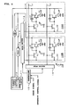
- FIG. 3 mainly illustrates the structure of a part of a light emitting display device (light emitting display panel) according to the present invention.
- the embodiment shown in this FIG. 3 shows the state where a light emitting display area 10A in which light emitting display pixels 10a are arranged in a matrix pattern and a measuring pixel area 10B in which measuring pixels 10b are arranged in a row direction are formed on a light emitting display panel 10.
- data lines m1, m2, m3, ... from a data driver which will be described later are arranged in a vertical direction (row direction), and control lines n1, n2, n3, ... from a scan driver which will be described later similarly are arranged in a horizontal direction (line direction). Further, in the display panel 10, power supply lines p1, p2, p3, ... are arranged in the vertical direction corresponding to the respective data lines.
- the light emitting display pixels 10a in the light emitting display area 10A are constructed by a conductance control technique as a typical example thereof. That is, as reference characters are assigned to respective elements constructing a pixel 10a on the upper left of the light emitting display area 10A, the gate of a control TFT (Tr1) comprised of N-channels is connected to the control line n1, and the source thereof is connected to the data line m2. The drain of the control TFT (Tr1) is connected to the gate of a drive TFT (Tr2) comprised of P-channels and to one terminal of a capacitor C1 provided for holding electrical charges.
- the source of the drive TFT (Tr2) is connected to the other terminal of the capacitor C1 and to the power supply line p2.
- the anode terminal of an organic EL element E1 provided as a light emitting element is connected to the drain of the drive TFT, and the cathode terminal of this EL element E1 is connected to a reference potential (ground).
- a large number of light emitting display pixels 10a of the above-described structure are arranged in a matrix pattern in the vertical and horizontal directions in the light emitting display area 10A as described above.
- the measuring pixels 10b in the measuring pixel area 10B are also constructed similarly to the light emitting display pixels, and the same reference characters as those of the respective elements constituting the light emitting display pixel 10a are assigned to the respective elements in the measuring pixel of the top thereof.
- the gate of the control TFT (Tr1) constructing the measuring pixel 10b is connected to the control line n1, and the source thereof is connected to the data line m1.
- the source of the drive TFT (Tr2) is connected to the power supply lines p1.
- the measuring pixels 10b are arranged forming a line along one data line m1 in the measuring pixel area 10B.
- the element designated by the reference character E1 constituting the measuring pixel 10b will be called a measuring element.
- the same element as the organic EL element E1 constituting the light emitting display pixel 10a is employed as the measuring element.
- the organic EL element when this element is driven, since the driving is accompanied by light emitting operation, it is desired that a shield film or the like which cuts off light is provided on the surface of the measuring pixel area 10B as the need arises.
- the organic EL element needs not necessarily be employed as the measuring element, and measures such as that elements which do not emit light are formed in the measuring pixel area 10B can be considered. In short, other elements whose electrical characteristics including a characteristic regarding changes with time, temperature dependency, and the like are very similar to those of the organic EL element can be used as the measuring element.
- the respective light emitting display pixels 10a are arranged in a matrix pattern at intersection point positions between the data lines and the control lines, the measuring pixels 10b are arranged forming a line along one data line m1, and the respective control lines utilized in these measuring pixels 10b and the control lines n1, n2, n3, ... utilized in the light emitting display pixels 10a are shared. Accordingly, the gate voltage of the control TFT of the measuring pixel 10b and the gate voltage of the control TFT of the light emitting display pixel 10a become common, and as a result, the gate voltage of the drive TFT of the measuring pixel 10b and the gate voltage of the drive TFT of the light emitting display pixel 10a become common.
- a constant current is supplied to the power supply line p1 in the measuring pixel 10b via a constant current source 11.
- a voltage detecting terminal 12 is drawn between the constant current source 11 and the respective measuring pixels 10b, that is, from the power supply line p1 so that the forward voltage VF of the measuring element in the measuring pixel 10b can be obtained at said terminal 12.
- FIG. 3 shows a form in which the voltage detecting terminal 12 is particularly provided in order to obtain the forward voltage VF of the measuring element, this is for the sake of convenience in the explanation, and in reality there are cases in which for example one signal line in an IC circuit has the function of the voltage detecting terminal 12.
- a drive voltage from a power supply circuit constituting a constant voltage source which will be described later is supplied to the respective light emitting display pixels 10a via the respective power supply lines p2, p3, ..., and by this drive voltage lighting drive of the respective EL elements E1 provided as light emitting elements are selectively carried out.
- FIG. 4 shows a block structure including peripheral circuits which drive and control the light emitting display panel 10 of the above-described structure.
- the respective data lines m1, m2, m3, ... arranged in the vertical direction are drawn from the data driver 13, and the control lines n1, n2, n3, ... arranged in the horizontal direction are drawn from the scan driver 14.
- a control bus is connected from a controller IC 15 to the data driver 13 and to the scan driver 14, the data driver 13 and the scan driver 14 are controlled based on an image signal supplied to a controller IC, lighting drive of the respective light emitting display pixels 10a in the light emitting display area 10A are selectively carried out by operations described below, and as a result an image is reproduced in the light emitting display area 10A.
- the control TFT (Tr1) allows a current corresponding to a data voltage which is supplied from the data line m2 to the source thereof to flow from the source to the drain. Accordingly, in the period in which the gate of the control TFT (Tr1) is at the ON voltage, the capacitor C1 is charged, and its voltage is supplied to the gate of the drive TFT (Tr2).
- the drive TFT (Tr2) allows a current which is based on the gate voltage and the source voltage thereof to flow in the EL element E1 to drive the EL element so that the EL element emits light. That is, the drive TFT (Tr2) constant-current drives the EL element E1 so that the EL element E1 emits light.
- the control TFT (Tr1) When the gate of the control TFT (Tr1) becomes an OFF voltage, the control TFT (Tr1) becomes a so-called cutoff. Although the drain of the control TFT (Tr1) becomes in an open state, the gate voltage of the drive TFT (Tr2) is maintained by the charges accumulated in the capacitor C1, the drive TFT (Tr2) maintains the drive current until a next scan, and light emission of the EL element E1 is also maintained.
- a sampling/holding circuit 16 which samples and holds the voltage value VF (the forward voltage of the measuring element) which is brought to the voltage detecting terminal 12 shown in FIG. 4 is connected to the voltage detecting terminal 12. The output of the sampling/holding circuit 16 is supplied to a voltage control section 18 in a power supply circuit 17.
- the voltage control section 18 in the power supply circuit 17 controls the value of the constant voltage supplied to the power supply lines p2, p3, ... in response to a hold voltage by the sampling/holding circuit 16. That is, this is carried out so that the level of the drive voltage applied to the respective light emitting display pixels 10a is controlled in response to the forward voltage VF brought to the voltage detecting terminal 12.
- control is performed so as to increase the level of the drive voltage applied to the respective light emitting display pixels 10a when the forward voltage VF brought to the terminal 12 is high, and inversely control is performed so as to decrease the level of the drive voltage applied to the respective light emitting display pixels 10a when the forward voltage VF brought to the terminal 12 is low.
- the value of the drive voltage applied to the light emitting display pixel 10a is controlled, and the drive TFT (Tr2) in the light emitting display pixel 10a can drive the EL element E1 in the state where the drop voltage (VD) of the degree by which a constant current characteristic can be ensured is ensured.
- the value of the drive voltage applied to the light emitting display pixel 10a as well as fluctuation elements such as the variation part per hour (VL) of the forward voltage VF and the temperature change part (VT) of the VF of the EL element and the like are controlled, a power loss generated in the drive TFT (Tr2) in the light emitting display pixel 10a can be effectively restrained.
- the constant current source 11 in the structure shown in FIG. 4 is constructed so as to output a current of the degree which allows one measuring pixel 10b to emit light at a predetermined intensity.
- a constant current is applied to the respective measuring pixels 10b one after another in synchronization with the operations of lighting drive for the light emitting display pixels 10a. That is, control is performed so that current is not supplied from the constant current source 11 to the plurality of measuring pixels 10b at the same time.
- the sampling/holding circuit 16 By allowing the sampling/holding circuit 16 to have a time constant which is longer than the cycle by which the constant current is supplied to the measuring pixels 10b one after another, the forward voltage VF averaged in an analogous way in the respective measuring pixels 10b can be obtained at the voltage detecting terminal 12.
- control for the value of the drive voltage applied to the light emitting display pixels 10a can be performed based on the averaged voltage VF, and influence due to variations of the VF can be avoided.
- the drive TFT (Tr2) constructing the light emitting display pixel 10a is operated in a saturation region at a predetermined gate voltage, it is necessary for the drive TFT (Tr2) in the measuring pixel 10b to be operated in a linear region as a switching element. This has a meaning that detection of the forward voltage VF in the measuring pixel 10b is prevented from becoming inaccurate when an ON resistance of the drive TFT in the measuring pixel 10b is large.
- the embodiment shown in FIG. 4 is constructed in such a way that an intensity control signal is supplied to the controller IC 15 and that the light emission intensities of the respective light emitting display pixels 10a can be changed in response to this intensity control signal. That is, the intensity control signal is supplied to the controller IC 15 so that a control signal is sent from the controller IC 15 to the data driver 13, and the data driver 13 controls the source voltage applied to the control TFTs (Tr1) constructing the respective light emitting display pixels 10a based on the intensity control signal.
- the gate voltages of the drive TFTs (Tr2) in the respective light emitting display pixels 10a are controlled, and the values of the currents supplied to the EL elements E1 in the light emitting display pixels 10a are changed. Therefore, as a result, the light emission intensities of the EL elements in the light emitting display pixels 10a are controlled.
- the drive current supplied to the measuring elements constituting the measuring pixels 10b is also controlled based on the intensity control signal.
- the current value of the constant current source 11 supplying current to the measuring pixels 10b is also changed by the intensity control signal.
- the forward voltage VF of the EL element E1 in the light emitting display pixel 10a can be grasped by the measuring element in the measuring pixel 10b more accurately.
- restraining function for the above-mentioned power loss generated in the drive TFT (Tr2) in the light emitting display pixel 10a can be realized with higher accuracy.
- the forward voltages VF obtained by the respective measuring pixels 10b are sampled and held and analog control for the drive voltage applied to the light emitting display pixel 10a is performed based on that hold value, for example it is also possible that A/D conversion for that hold value is performed to obtain digital data to control the drive voltage applied to the light emitting display pixels 10a based on the digital data.
- averaging process for the forward voltages VF can be made easy, and in the case where a part of the measuring pixels 10b becomes defective, processing such as stopping of obtaining the VF from a pixel which has become defective can be performed easily.
- this invention not only can be adopted in a light emitting display device of this specified structure but also can be adopted similarly in a light emitting display device in which employed is an active drive type pixel structure such as for example a voltage writing technique, a current writing technique, a drive technique of 3 TFT method which realizes digital gradation, that is, SES (Simultaneous-Erasing-Scan), a threshold voltage correction technique, and a current mirror technique, and the like.
- an active drive type pixel structure such as for example a voltage writing technique, a current writing technique, a drive technique of 3 TFT method which realizes digital gradation, that is, SES (Simultaneous-Erasing-Scan), a threshold voltage correction technique, and a current mirror technique, and the like.
- the embodiment described above employs a structure in which electrical connection structures constructing the respective light emitting display pixels 10a and measuring pixels 10b are the same, the both structures may be different.
Landscapes
- Engineering & Computer Science (AREA)
- Physics & Mathematics (AREA)
- Computer Hardware Design (AREA)
- General Physics & Mathematics (AREA)
- Theoretical Computer Science (AREA)
- Control Of Indicators Other Than Cathode Ray Tubes (AREA)
- Electroluminescent Light Sources (AREA)
- Control Of El Displays (AREA)
- Devices For Indicating Variable Information By Combining Individual Elements (AREA)
Applications Claiming Priority (2)
| Application Number | Priority Date | Filing Date | Title |
|---|---|---|---|
| JP2003040811A JP4571375B2 (ja) | 2003-02-19 | 2003-02-19 | アクティブ駆動型発光表示装置およびその駆動制御方法 |
| JP2003040811 | 2003-02-19 |
Publications (1)
| Publication Number | Publication Date |
|---|---|
| EP1450345A2 true EP1450345A2 (de) | 2004-08-25 |
Family
ID=32732936
Family Applications (1)
| Application Number | Title | Priority Date | Filing Date |
|---|---|---|---|
| EP04003140A Withdrawn EP1450345A2 (de) | 2003-02-19 | 2004-02-12 | Anzeigevorrichtung mit aktiver Matrix und Steuerverfahren dafür |
Country Status (6)
| Country | Link |
|---|---|
| US (1) | US7248255B2 (de) |
| EP (1) | EP1450345A2 (de) |
| JP (1) | JP4571375B2 (de) |
| KR (1) | KR100959085B1 (de) |
| CN (1) | CN100378778C (de) |
| TW (1) | TWI234757B (de) |
Cited By (4)
| Publication number | Priority date | Publication date | Assignee | Title |
|---|---|---|---|---|
| WO2007031704A1 (en) * | 2005-09-12 | 2007-03-22 | Cambridge Display Technology Limited | Active matrix display drive control systems |
| EP1598804A3 (de) * | 2004-05-22 | 2009-05-20 | Semiconductor Energy Laboratory Co., Ltd. | Anzeigegerät und elektronisches Gerät |
| EP1774500A4 (de) * | 2004-07-23 | 2009-07-15 | Semiconductor Energy Lab | Anzeigeeinrichtung und ansteuerverfahren dafür |
| US8692740B2 (en) | 2005-07-04 | 2014-04-08 | Semiconductor Energy Laboratory Co., Ltd. | Display device and driving method thereof |
Families Citing this family (27)
| Publication number | Priority date | Publication date | Assignee | Title |
|---|---|---|---|---|
| JP2005084260A (ja) * | 2003-09-05 | 2005-03-31 | Agilent Technol Inc | 表示パネルの変換データ決定方法および測定装置 |
| JP4836402B2 (ja) * | 2003-09-29 | 2011-12-14 | 東北パイオニア株式会社 | 自発光型表示装置 |
| JP4850436B2 (ja) * | 2004-05-21 | 2012-01-11 | 株式会社半導体エネルギー研究所 | 表示装置及びそれを用いた電子機器 |
| JP4539963B2 (ja) * | 2004-06-10 | 2010-09-08 | 東北パイオニア株式会社 | アクティブ駆動型発光表示装置および同表示装置を搭載した電子機器 |
| US7812794B2 (en) * | 2004-12-06 | 2010-10-12 | Semiconductor Energy Laboratory Co., Ltd. | Display device and driving method thereof |
| JP4753351B2 (ja) * | 2005-03-15 | 2011-08-24 | 東北パイオニア株式会社 | 発光表示パネルの駆動装置及びその駆動方法 |
| JP4749010B2 (ja) * | 2005-03-17 | 2011-08-17 | 東北パイオニア株式会社 | アクティブマトリクス型発光表示パネルの駆動装置および駆動方法 |
| JP4707090B2 (ja) * | 2005-03-28 | 2011-06-22 | 東北パイオニア株式会社 | 発光表示パネルの駆動装置 |
| JP5164331B2 (ja) * | 2005-03-31 | 2013-03-21 | 株式会社半導体エネルギー研究所 | 表示装置、表示モジュール、および電子機器 |
| JP5177960B2 (ja) * | 2005-04-11 | 2013-04-10 | 株式会社半導体エネルギー研究所 | 表示装置及びそれを用いた電子機器 |
| JP5238140B2 (ja) * | 2005-05-02 | 2013-07-17 | 株式会社半導体エネルギー研究所 | 発光装置 |
| JP4811849B2 (ja) * | 2005-05-19 | 2011-11-09 | 東北パイオニア株式会社 | 発光表示パネルの駆動装置および駆動方法 |
| JP2006343531A (ja) * | 2005-06-09 | 2006-12-21 | Tohoku Pioneer Corp | 発光パネルの駆動装置および駆動方法 |
| JP5222464B2 (ja) * | 2005-07-04 | 2013-06-26 | 株式会社半導体エネルギー研究所 | 表示装置及び電子機器 |
| JP5084003B2 (ja) * | 2005-10-28 | 2012-11-28 | 東北パイオニア株式会社 | 発光表示パネルの駆動装置および駆動方法 |
| CN100557668C (zh) * | 2006-11-14 | 2009-11-04 | 中华映管股份有限公司 | 驱动装置 |
| KR100914118B1 (ko) * | 2007-04-24 | 2009-08-27 | 삼성모바일디스플레이주식회사 | 유기 전계 발광 표시 장치 및 그 구동 방법 |
| JP2009025741A (ja) * | 2007-07-23 | 2009-02-05 | Hitachi Displays Ltd | 画像表示装置とその画素劣化補正方法 |
| JP2009031711A (ja) * | 2007-07-27 | 2009-02-12 | Samsung Sdi Co Ltd | 有機電界発光表示装置及びその駆動方法 |
| US8139007B2 (en) * | 2008-03-31 | 2012-03-20 | Casio Computer Co., Ltd. | Light-emitting device, display device, and method for controlling driving of the light-emitting device |
| JP2010002498A (ja) * | 2008-06-18 | 2010-01-07 | Sony Corp | パネルおよび駆動制御方法 |
| KR20120043094A (ko) * | 2009-08-13 | 2012-05-03 | 이 아이 듀폰 디 네모아 앤드 캄파니 | 전자 소자 내 픽셀을 위한 전기 구동 방식 |
| TWI427606B (zh) * | 2009-10-20 | 2014-02-21 | Au Optronics Corp | 具畫素資料自我保持機能之液晶顯示裝置與其靜止模式運作方法 |
| US8487844B2 (en) * | 2010-09-08 | 2013-07-16 | Semiconductor Energy Laboratory Co., Ltd. | EL display device and electronic device including the same |
| US8928560B2 (en) | 2012-03-20 | 2015-01-06 | Hewlett-Packard Development Company, L.P. | Display matrix with resistance switches |
| CN103426369B (zh) * | 2013-08-27 | 2015-11-11 | 京东方科技集团股份有限公司 | 显示屏 |
| KR20230156612A (ko) * | 2022-05-06 | 2023-11-14 | 삼성전자주식회사 | 디스플레이 장치 및 그 제어 방법 |
Family Cites Families (16)
| Publication number | Priority date | Publication date | Assignee | Title |
|---|---|---|---|---|
| US4782340A (en) * | 1986-08-22 | 1988-11-01 | Energy Conversion Devices, Inc. | Electronic arrays having thin film line drivers |
| JP3313830B2 (ja) | 1993-07-19 | 2002-08-12 | パイオニア株式会社 | 表示装置の駆動回路 |
| US5952789A (en) * | 1997-04-14 | 1999-09-14 | Sarnoff Corporation | Active matrix organic light emitting diode (amoled) display pixel structure and data load/illuminate circuit therefor |
| JP4841754B2 (ja) * | 2000-06-13 | 2011-12-21 | 株式会社半導体エネルギー研究所 | アクティブマトリクス型の発光装置、及び電子機器 |
| CN1892774A (zh) * | 2000-07-07 | 2007-01-10 | 精工爱普生株式会社 | 用于有机场致发光显示器的电流抽样电路 |
| US6919868B2 (en) * | 2000-07-07 | 2005-07-19 | Seiko Epson Corporation | Circuit, driver circuit, electro-optical device, organic electroluminescent display device electronic apparatus, method of controlling the current supply to a current driven element, and method for driving a circuit |
| JP3437152B2 (ja) * | 2000-07-28 | 2003-08-18 | ウインテスト株式会社 | 有機elディスプレイの評価装置および評価方法 |
| JP4884609B2 (ja) * | 2000-08-10 | 2012-02-29 | 株式会社半導体エネルギー研究所 | 表示装置及びその駆動方法、並びに電子機器 |
| SG114502A1 (en) * | 2000-10-24 | 2005-09-28 | Semiconductor Energy Lab | Light emitting device and method of driving the same |
| SG111928A1 (en) * | 2001-01-29 | 2005-06-29 | Semiconductor Energy Lab | Light emitting device |
| SG107573A1 (en) * | 2001-01-29 | 2004-12-29 | Semiconductor Energy Lab | Light emitting device |
| JP2002351403A (ja) * | 2001-05-30 | 2002-12-06 | Toshiba Corp | 画像表示装置 |
| JP2003043998A (ja) * | 2001-07-30 | 2003-02-14 | Pioneer Electronic Corp | ディスプレイ装置 |
| JP4067878B2 (ja) * | 2002-06-06 | 2008-03-26 | 株式会社半導体エネルギー研究所 | 発光装置及びそれを用いた電気器具 |
| JP3942169B2 (ja) * | 2002-08-29 | 2007-07-11 | 東北パイオニア株式会社 | 発光表示パネルの駆動装置および駆動方法 |
| US7079092B2 (en) * | 2003-04-25 | 2006-07-18 | Barco Nv | Organic light-emitting diode (OLED) pre-charge circuit for use in a common anode large-screen display |
-
2003
- 2003-02-19 JP JP2003040811A patent/JP4571375B2/ja not_active Expired - Lifetime
-
2004
- 2004-01-30 TW TW093102234A patent/TWI234757B/zh not_active IP Right Cessation
- 2004-02-04 US US10/770,394 patent/US7248255B2/en not_active Expired - Fee Related
- 2004-02-12 EP EP04003140A patent/EP1450345A2/de not_active Withdrawn
- 2004-02-16 KR KR1020040009966A patent/KR100959085B1/ko not_active Expired - Lifetime
- 2004-02-19 CN CNB2004100054703A patent/CN100378778C/zh not_active Expired - Lifetime
Cited By (11)
| Publication number | Priority date | Publication date | Assignee | Title |
|---|---|---|---|---|
| EP1598804A3 (de) * | 2004-05-22 | 2009-05-20 | Semiconductor Energy Laboratory Co., Ltd. | Anzeigegerät und elektronisches Gerät |
| US8111215B2 (en) | 2004-05-22 | 2012-02-07 | Semiconductor Energy Laboratory Co., Ltd. | Display device and electronic device |
| EP1774500A4 (de) * | 2004-07-23 | 2009-07-15 | Semiconductor Energy Lab | Anzeigeeinrichtung und ansteuerverfahren dafür |
| US8134546B2 (en) | 2004-07-23 | 2012-03-13 | Semiconductor Energy Laboratory Co., Ltd. | Display device and driving method thereof |
| US8482493B2 (en) | 2004-07-23 | 2013-07-09 | Semiconductor Energy Laboratory Co., Ltd. | Display device and driving method thereof |
| US8692740B2 (en) | 2005-07-04 | 2014-04-08 | Semiconductor Energy Laboratory Co., Ltd. | Display device and driving method thereof |
| WO2007031704A1 (en) * | 2005-09-12 | 2007-03-22 | Cambridge Display Technology Limited | Active matrix display drive control systems |
| GB2443372A (en) * | 2005-09-12 | 2008-04-30 | Cambridge Display Tech Ltd | Active matrix display drive control systems |
| GB2443372B (en) * | 2005-09-12 | 2010-04-28 | Cambridge Display Tech Ltd | Active matrix display drive control systems |
| CN101263543B (zh) * | 2005-09-12 | 2011-03-02 | 剑桥显示技术有限公司 | 有源矩阵显示器驱动控制系统 |
| US8860708B2 (en) | 2005-09-12 | 2014-10-14 | Cambridge Display Technology Limited | Active matrix display drive control systems |
Also Published As
| Publication number | Publication date |
|---|---|
| CN1523558A (zh) | 2004-08-25 |
| CN100378778C (zh) | 2008-04-02 |
| US7248255B2 (en) | 2007-07-24 |
| KR100959085B1 (ko) | 2010-05-20 |
| JP2004252036A (ja) | 2004-09-09 |
| US20040160395A1 (en) | 2004-08-19 |
| JP4571375B2 (ja) | 2010-10-27 |
| KR20040074607A (ko) | 2004-08-25 |
| TW200416664A (en) | 2004-09-01 |
| TWI234757B (en) | 2005-06-21 |
Similar Documents
| Publication | Publication Date | Title |
|---|---|---|
| US7248255B2 (en) | Active drive type light emitting display device and drive control method thereof | |
| US11164520B2 (en) | Power off method of display device, and display device | |
| US6756951B1 (en) | Display apparatus and driving circuit of display panel | |
| US7199768B2 (en) | Display apparatus controlling brightness of current-controlled light emitting element | |
| JP4409821B2 (ja) | El表示装置 | |
| CN101960509B (zh) | 显示装置及其控制方法 | |
| US7786989B2 (en) | Electronic circuit, method of driving electronic circuit, electro-optical device, method of driving electro-optical device, and electronic apparatus | |
| JP4195337B2 (ja) | 発光表示装置及びその表示パネルと駆動方法 | |
| US7046220B2 (en) | Display and driving method thereof | |
| KR101046415B1 (ko) | 화소회로 및 표시장치 | |
| TWI284307B (en) | Electronic circuit and driving method thereof, electronic device, photoelectric apparatus and driving method thereof, and electronic machine | |
| US7557802B2 (en) | Self light emitting type display device | |
| US8125417B2 (en) | Display driver circuit for driving a light-emitting device with the threshold offset of a drive transistor compensated for | |
| US8692746B2 (en) | Image display device for reducing the amount of time required to perform plural, consecutive threshold voltage correction operations | |
| US7196681B2 (en) | Driving circuit for light emitting elements | |
| KR20060015571A (ko) | 임계 전압의 드리프트를 보상하는 능동 매트릭스 oled디스플레이 디바이스 | |
| CN104637445A (zh) | Amoled像素驱动电路及像素驱动方法 | |
| US7508364B2 (en) | Image display device | |
| KR100658672B1 (ko) | 유기 전계발광 표시장치 및 그의 구동방법 | |
| US20080297056A1 (en) | Light emitting element circuit and drive method thereof | |
| CN100428312C (zh) | 电致发光显示装置及其驱动方法 | |
| KR20080090954A (ko) | 유기전계 발광표시장치의 화소구동 방법 및 장치 | |
| JP2002358049A (ja) | 発光素子の駆動回路、及びアクティブマトリクス型表示パネル | |
| KR101519445B1 (ko) | 전압보상형 화소회로 및 그 구동방법 | |
| JP4539963B2 (ja) | アクティブ駆動型発光表示装置および同表示装置を搭載した電子機器 |
Legal Events
| Date | Code | Title | Description |
|---|---|---|---|
| PUAI | Public reference made under article 153(3) epc to a published international application that has entered the european phase |
Free format text: ORIGINAL CODE: 0009012 |
|
| AK | Designated contracting states |
Kind code of ref document: A2 Designated state(s): AT BE BG CH CY CZ DE DK EE ES FI FR GB GR HU IE IT LI LU MC NL PT RO SE SI SK TR |
|
| AX | Request for extension of the european patent |
Extension state: AL LT LV MK |
|
| STAA | Information on the status of an ep patent application or granted ep patent |
Free format text: STATUS: THE APPLICATION HAS BEEN WITHDRAWN |
|
| 18W | Application withdrawn |
Effective date: 20080109 |