EP1439581A2 - Verbindungsstruktur - Google Patents
Verbindungsstruktur Download PDFInfo
- Publication number
- EP1439581A2 EP1439581A2 EP03258223A EP03258223A EP1439581A2 EP 1439581 A2 EP1439581 A2 EP 1439581A2 EP 03258223 A EP03258223 A EP 03258223A EP 03258223 A EP03258223 A EP 03258223A EP 1439581 A2 EP1439581 A2 EP 1439581A2
- Authority
- EP
- European Patent Office
- Prior art keywords
- conductive
- interconnect elements
- further characterized
- conductive layer
- subset
- Prior art date
- Legal status (The legal status is an assumption and is not a legal conclusion. Google has not performed a legal analysis and makes no representation as to the accuracy of the status listed.)
- Withdrawn
Links
Images


Classifications
-
- H—ELECTRICITY
- H05—ELECTRIC TECHNIQUES NOT OTHERWISE PROVIDED FOR
- H05K—PRINTED CIRCUITS; CASINGS OR CONSTRUCTIONAL DETAILS OF ELECTRIC APPARATUS; MANUFACTURE OF ASSEMBLAGES OF ELECTRICAL COMPONENTS
- H05K1/00—Printed circuits
- H05K1/02—Details
- H05K1/0213—Electrical arrangements not otherwise provided for
- H05K1/0216—Reduction of cross-talk, noise or electromagnetic interference
- H05K1/0218—Reduction of cross-talk, noise or electromagnetic interference by printed shielding conductors, ground planes or power plane
- H05K1/0219—Printed shielding conductors for shielding around or between signal conductors, e.g. coplanar or coaxial printed shielding conductors
-
- H10W70/635—
-
- H10W70/658—
-
- H10W72/00—
-
- H10W90/401—
-
- H—ELECTRICITY
- H05—ELECTRIC TECHNIQUES NOT OTHERWISE PROVIDED FOR
- H05K—PRINTED CIRCUITS; CASINGS OR CONSTRUCTIONAL DETAILS OF ELECTRIC APPARATUS; MANUFACTURE OF ASSEMBLAGES OF ELECTRICAL COMPONENTS
- H05K1/00—Printed circuits
- H05K1/02—Details
- H05K1/11—Printed elements for providing electric connections to or between printed circuits
- H05K1/111—Pads for surface mounting, e.g. lay-out
- H05K1/112—Pads for surface mounting, e.g. lay-out directly combined with via connections
- H05K1/113—Via provided in pad; Pad over filled via
-
- H—ELECTRICITY
- H05—ELECTRIC TECHNIQUES NOT OTHERWISE PROVIDED FOR
- H05K—PRINTED CIRCUITS; CASINGS OR CONSTRUCTIONAL DETAILS OF ELECTRIC APPARATUS; MANUFACTURE OF ASSEMBLAGES OF ELECTRICAL COMPONENTS
- H05K2201/00—Indexing scheme relating to printed circuits covered by H05K1/00
- H05K2201/07—Electric details
- H05K2201/0707—Shielding
- H05K2201/0715—Shielding provided by an outer layer of PCB
-
- H—ELECTRICITY
- H05—ELECTRIC TECHNIQUES NOT OTHERWISE PROVIDED FOR
- H05K—PRINTED CIRCUITS; CASINGS OR CONSTRUCTIONAL DETAILS OF ELECTRIC APPARATUS; MANUFACTURE OF ASSEMBLAGES OF ELECTRICAL COMPONENTS
- H05K2201/00—Indexing scheme relating to printed circuits covered by H05K1/00
- H05K2201/09—Shape and layout
- H05K2201/09209—Shape and layout details of conductors
- H05K2201/095—Conductive through-holes or vias
- H05K2201/09618—Via fence, i.e. one-dimensional array of vias
-
- H—ELECTRICITY
- H05—ELECTRIC TECHNIQUES NOT OTHERWISE PROVIDED FOR
- H05K—PRINTED CIRCUITS; CASINGS OR CONSTRUCTIONAL DETAILS OF ELECTRIC APPARATUS; MANUFACTURE OF ASSEMBLAGES OF ELECTRICAL COMPONENTS
- H05K2201/00—Indexing scheme relating to printed circuits covered by H05K1/00
- H05K2201/10—Details of components or other objects attached to or integrated in a printed circuit board
- H05K2201/10613—Details of electrical connections of non-printed components, e.g. special leads
- H05K2201/10621—Components characterised by their electrical contacts
- H05K2201/10734—Ball grid array [BGA]; Bump grid array
-
- H—ELECTRICITY
- H05—ELECTRIC TECHNIQUES NOT OTHERWISE PROVIDED FOR
- H05K—PRINTED CIRCUITS; CASINGS OR CONSTRUCTIONAL DETAILS OF ELECTRIC APPARATUS; MANUFACTURE OF ASSEMBLAGES OF ELECTRICAL COMPONENTS
- H05K3/00—Apparatus or processes for manufacturing printed circuits
- H05K3/30—Assembling printed circuits with electric components, e.g. with resistor
- H05K3/32—Assembling printed circuits with electric components, e.g. with resistor electrically connecting electric components or wires to printed circuits
- H05K3/34—Assembling printed circuits with electric components, e.g. with resistor electrically connecting electric components or wires to printed circuits by soldering
- H05K3/341—Surface mounted components
- H05K3/3431—Leadless components
- H05K3/3436—Leadless components having an array of bottom contacts, e.g. pad grid array or ball grid array components
-
- H10W70/20—
-
- H10W72/07251—
-
- H10W72/20—
Definitions
- This invention relates to interconnection of electronic devices such as integrated circuits and printed circuit boards.
- Electronic assemblies typically comprise a plurality of components, such as semiconductor integrated circuits, including MOSFET power transistors, mounted to a substrate such as a printed circuit board (PCB) or ceramic plate.
- the substrate can include patterns of conductive elements (e.g., pads, traces, and/or planes) to interconnect the substrate to the components in a predetermined way.
- conductive elements e.g., pads, traces, and/or planes
- a semiconductor die can be wire-bonded to a lead-frame and over-molded in a package having a standardized footprint.
- the lead-frame can include a number of conductive leads that are soldered to pads on the surface of the substrate.
- DIP dual-in-line
- SO small-outline
- the overall volume of the packaged device is usually significantly greater than the volume of the semiconductor die within the package.
- power devices e.g., low voltage MOSFET power transistors
- such packages typically exhibit significant lead interconnect resistance and inductance.
- Semiconductor components may also be mounted directly to the substrate.
- One way to do this is to directly connect conductive pads (e.g., pads 10a, 10b, 10c) on the surface of the substrate 12 to interconnection pads (not shown) on the surface of a semiconductor die 14 by use of area array interconnects (e.g., ball-grid array interconnects 16a, 16b, and 16c).
- the area array interconnects may be made, e.g., of solder or conductive epoxy. Stud bumps may also be used.
- the assembly method shown in Figure 1 is sometimes referred to as a "flip-chip" assembly.
- a plurality of interconnections on the surface of a die are made to form a component termination.
- a component is a power MOSFET, which can include a plurality (in some cases, many thousands) of active cells, each cell comprising a drain, source and gate termination.
- the drain terminal of the component can be formed by connecting essentially all of the drain terminals of the active cells together.
- the source and gate terminals can be formed by connecting essentially all of the source and gate terminals of the active cells together.
- FIG. 13A shows an example of a vertical DMOS power MOSFET die 200 comprising a ball-grid array of interconnects.
- a vertical MOSFET comprises a plurality of active cells that carry current vertically within a die (as indicated by the arrow in the Figure labeled "current flow").
- a first surface of the die can include a plurality of drain contacts and a second surface comprises a plurality of source and gate contacts.
- the plurality of low power gate contacts are connected together by metallization (not shown) on the second surface of the die and brought out to a ball-grid gate interconnect contact, e.g., interconnect 205 in Figure 13A.
- Individual source contacts are also brought out to an array of ball-grid source interconnects 204 on the second surface of the die 200.
- the array of drain contacts on the first surface of the die are connected together by a sheet of drain contact metallization 202.
- a sheet of drain contact metallization 202 One way to package such a device is shown in Figure 13B.
- the drain contact metallization 202 is connected (e.g., by solder, not shown) to a conductive frame 206.
- Ball grid contacts, such as source interconnects 204 on the die 200 and drain interconnects 207 on the frame extend from the bottom of the assembly comprising the die and the frame.
- the device of Figure 13B may be mounted to a printed circuit board 209 by connecting the drain interconnects 207 and the source interconnects 204 to drain etch planes 211 and source etch plane 213 on the surface of the board 209 (the gate interconnect is not shown).
- Fairchild Semiconductor Corporation South Portland, ME, U.S.A., manufactures a device of the kind shown in Figure 13A, as part number FDZ201N, "N-channel 2.5 V Specified
- Lateral power MOSFET devices are also known. Such devices can include a plurality of active cells comprising drain, source, and gate terminals that are connected in parallel. However, unlike the vertical MOSFET discussed above, the current in the cells of a lateral MOSFET flows horizontally within the die. Thus, all of the gate, source, and drain contacts can reside on the same surface of the die.
- the packaging and mounting techniques shown in Figures 13 and 14 are not adapted for use with such a lateral device, particularly in cases where the source and drain contacts are disposed on the same side of the die.
- Lateral power MOSFET devices may provide an effective channel ON state resistance lower than 1000 micro-Ohm within a die measuring 3mm x 3mm. Owing to the relatively high resistance per square of thin metal interconnect layers available on silicon, proximity of source and drain terminals to all active cells within the die is required to achieve comparably low values of effective device ON state resistance. By distributing across the mounting surface of the die a set of interconnect elements, including a subset of drain interconnect elements and a subset of source interconnect elements with alternating source and drain elements, such as with a high density ball grid array (BGA) having a source and drain ball pitch of 0.5 mm or less, low values of effective device ON state resistance may be retained.
- BGA ball grid array
- the interconnect architecture should achieve a substrate interconnect resistance substantially lower than 500 micro-Ohm to adequately support a lateral power MOSFET device having a 1000 micro-Ohm ON state resistance.
- the method generally consists of arranging individual interconnections on the die so that the ball-grid array forms rows of source and drain connections that are generally parallel to the edges of the die. Linear rows of balls connected to MOSFET drains alternate with generally linear rows of balls connected to MOSFET sources.
- the substrate onto which the balls are placed comprises interdigitated fingers of conductive etch on the top side of the substrate.
- the interdigitated fingers of conductive etch connect the alternating rows together so as to create a conductive region on the top side of the substrate that connects together all of the MOSFET sources and another conductive region on the top side which connects together all of the MOSFET drains.
- the interconnect architecture outlined above gives rise to a high substrate interconnect resistance and losses higher than the acceptable limit specified above.
- an interconnect architecture in which a substrate such as a printed circuit board includes multiple conductive layers separated by one or more interposed insulating layers, the conductive layers being adapted to receive a high density array of interconnect elements such as a BGA.
- a printed circuit board may provide a very low resistance interconnect forming the drain and source terminals of a lateral power MOSFET device incorporating a high density array of alternating source and drain interconnect elements, such as a BGA.
- source and drain currents may be routed on different conductive layers separated by one or more interposed insulating layers.
- the upper conductive layer may include laterally non-conductive regions accommodating conductive columns conforming to the locations of a subset of the interconnect elements, the subset being associated with either the drain terminal or source terminal, and passing through the insulating layer to connect a lower conductive layer to the interconnect elements of that subset.
- the aggregate interconnect resistance in such embodiments, including connections from the multiplicity of source and drain balls under the FET to a conductive edge along the periphery of the FET die, may be 200 micro-Ohm or lower.
- FIGS. 1A and 1B show, respectively, an exploded perspective view and a perspective view of a flip-chip assembly.
- FIG. 2 shows an arrangement of interconnections on a semiconductor device.
- FIG. 3A is a perspective view of a substrate, partially cut away, viewed from the top.
- FIG. 3B is a cross-section of the substrate along the line A-A in Fig. 3A.
- FIGS. 4A and 4B show cross-sectional views of a semiconductor device having a solder ball-grid array of interconnections mounted on a substrate before and after solder reflow, respectively.
- FIG. 5 shows currents flowing in an arrangement of source and drain metal traces on a patterned die.
- FIG. 6 shows current flowing through etches on a printed circuit board.
- FIG. 7 shows a perspective view of a substrate.
- FIGS. 8 and 9 show cross-sectional views of substrates.
- FIG. 10 shows a bottom view of a semiconductor device having interconnects thereon.
- FIG. 11 shows an exploded perspective view of an assembly comprising a MOSFET device and a circuit board.
- FIG. 12 shows a partial cross-section of the circuit board of FIG. 11.
- FIGS. 13A and 13B show, respectively, a perspective view of a vertical MOSFET die and a side view of the die contained within a package.
- FIG. 14 shows a perspective view of the packaged die of FIG. 13B mounted to a substrate.
- Figures 2 shows a surface of a semiconductor die 14 having ball-grid contacts 17 and 19.
- the semiconductor die 14 is of the kind for which a first termination to the die requires that low resistance connections be made to a first subset of balls on a surface of the die; a second termination to the die requires that low resistance connections be made to a second subset of balls on the same surface of the die; and the balls that form the first termination are arranged in a pattern which alternates with the pattern of the balls which form the second termination.
- the example shown in FIG. 2 is a lateral MOSFET.
- the source solder balls 17 and the drain balls 19 are on the same surface of the die and alternate within rows and columns that are generally parallel to the edges of the die 14.
- the source and drain balls 17 and 19 form an alternating pattern in which the interconnect pattern for the source termination and the interconnect pattern for a drain termination differ only in terms of spatial offset or angularrotation.
- the die 14 might also include additional terminations.
- the semiconductor die 14 may contain a MOSFET switch, as well as other circuitry.
- the terminations on such a die might include the source and drain terminals for the MOSFET as well as one or more power and ground terminals for the other circuitry.
- balls comprising more than two terminations e.g., source, drain, power, ground
- the pitch of the source balls 17 and the pitch of the drain balls 19 is the same. In the arrangement shown in FIG. 2, however, the pitch between the source balls 17 is increased by a factor of ⁇ 2 (square root of 2). Similarly, the pitch of the drain balls 19 is increased by ⁇ 2. In other embodiments wherein the source and drain solder balls 17 and 19 are not in an aligned checkerboard pattern, the respective pitches of the source and drain solder balls 17 and 19 can be increased by a factor of about 1.1 or more.
- Low voltage lateral MOSFET switching power devices can achieve lower values of ON resistance than can be achieved with certain vertical MOSFET devices.
- all of the connections to a lateral MOSFET are typically on one surface of the die.
- a low ON resistance lateral MOSFET typically includes an array of interconnect elements to provide source and drain connections in relative proximity to the MOSFET cells. To fully exploit the potential for low in-circuit resistance of the lateral MOSFET, the aggregate resistance of the interconnections between the lateral MOSFET and the substrate to which it is mounted may be made very low.
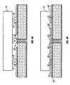
- FIGS. 3A and 3B A portion of a substrate 20 for achieving efficient termination of the die 14 of Figure 2 is illustrated in Figures 3A and 3B.
- the substrate 20 comprises a two-layer printed circuit board 23 with a top conductive layer 24, a bottom conductive layer 26, and a non-conductive core 13.
- a non-conductive solder mask 22 (shown in Fig. 3B) on the top of the substrate 20 is cleared away in regions 27 to form "solder-mask-defined" locations for connection to, e.g., drain solder balls 19 on the die 14 shown in Fig. 2.
- the solder mask 22 is also cleared away in regions 25 to create mask-free regions around pads 28.
- the solder mask can be configured to cover the exposed edges of the conductive layer 27 that are exposed at regions 25.
- Pads 28 form "pad-defined” locations for connection to, e.g., source solder balls 17 on the die 14 of Fig. 2.
- Pad 28 connects to column 29, which is plated on to the inside surface of a hole 45 (shown in Fig. 3B) in the core 13 to connect pad 28 to bottom conductive layer 26.
- a hole 45 shown in Fig. 3B
- both the diameter of the column 29 and the size of the through hole 30 may be kept small.
- Figures 4A and 4B show, respectively, partial cross-sectional views of a die of the kind shown in Fig. 3A mounted to a substrate of the kind shown in Fig. 2, before and after reflowing the solder balls 17 and 19.
- drain solder balls 19 lie in solder-mask-defined regions 27 and source solder balls 17 lie in pad-defined regions 25.
- the solder balls 17 and 19 have been reflowed to form soldered drain connections 31 and soldered source connections 33 between the die 14 and the top conductive layer 24. In certain embodiments, the solder will wet only to the exposed pad, and will not wet to the exposed non-conductive core 13.
- Figure 5 shows the top conductive layer of a printed circuit board with an interdigitated termination etch architecture.
- Figure 6 shows the top conductive layer of a printed circuit board using the termination etch arrangement (as described above with reference to Figures 3 and 4).
- the pattern of conductive elements is arranged in each of Figures 5 and 6 to terminate the source and drain connections of a MOSFET die of the kind shown in Figure 2.
- the locations of the drain solder ball connections are indicated by the circles marked "D” and the locations of the source solder ball connections are indicated by the circles marked "S.”
- the locations of the drain solder ball connections are indicated by the circles marked "D” and the source solder balls are connected to source pads 28.
- the drain termination etch 40 comprising drain etch fingers 40a - 40d is interdigitated with the source termination etch 42, comprising source etch fingers 42a - 42c.
- Current that flows into the drain termination etch 40 flows out of the source termination etch 42, as indicated by the arrows in Figure 5.
- Current is constrained to flow along the paths defined by the etch fingers, which results in voltage drops along the length of the etch fingers 40 and 42.
- both the drain and source termination etches 40 and 42 are on one side of the circuit board, a portion of the periphery of the interconnection etch pattern must be reserved to carry the flow of drain current into the die (i.e., peripheral etch regions 43a and 43b) and the remainder of the periphery must be reserved for source current to flow out of the die (i.e., peripheral etch regions 43c and 43d). Because the currents in the source and drain are essentially identical, losses will be minimized if half of the periphery is reserved for the source current and the other half for the drain current.
- the interconnect architecture of Figure 6 essentially all of the top conductive layer 24 is available to carry current into the drain solder ball connections, with the exception being the laterally non-conductive regions 25 that surround the source solder ball pads 28. Furthermore, the etch pattern of Fig. 6 allows current to efficiently flow into the drain from three or four of the peripheral etch regions 43a-43d. In contrast, no more than two of the peripheral etch regions could be utilized to efficiently carry current into the drain in the etch pattern shown in Fig. 5.
- Fig. 6 can be applied to a semiconductor die in which the ball grid of contacts are arranged in alternating rows of like kinds.
- a substrate for such a device would use the same basic structural arrangement of the substrate 20 of Figure 3A. Differences may include, for example, the relative locations of the regions 27 which form the "solder-mask-defined" locations for connection to, e.g., the drain solder balls 19 and the locations of the pads 28 for connection, e.g., to the source solder balls 17 and their respective cleared-away regions 25.
- the interconnect structure of Figure 3A (which is compatible with MOSFET embodiments wherein the source balls and the drain balls alternate within rows and columns that are generally parallel to the edges of the die) may exhibit a lower overall resistance than the interconnect structure of Figure 7 (which is compatible with MOSFET embodiments wherein linear rows of balls connected to MOSFET drains alternate with linear rows of balls connected to MOSFET sources), owing to the larger spacing between regions 25 on the surface of the substrate. This larger spacing is due to the regions 25 being located along diagonals in the array of Figure 3A as opposed to being arranged along a row or column, as shown in Figure 7.
- the distance between the center of source interconnect elements in Figure 3A is approximately ⁇ 2 greater than the distance between the center of interconnect elements of source interconnect elements in Figure 7.
- the pitch of the non-conductive regions 25 is made finer and approaches the diameter of the laterally non-conductive regions 25, current flow in between laterally non-conductive regions is pinched off. This pinch off effect causes the interconnect structure of Figure 7 to exhibit higher interconnect resistance than the interconnect structure of Figure 3A for a high density BGA.
- a substantial reduction in interconnect resistance relative to the interconnect architecture of Figure 5 requires a minimum number of rows and columns of interconnect elements. Furthermore, the reduction in interconnect loss grows rapidly with the size of the array. Specifically, with only two rows and two columns of interconnect elements, there are a total of four interconnect elements.
- the ON state resistance of MOSFET devices having only four interconnect elements is relatively high and may constitute the limiting factor to the total in-circuit ON state resistance.
- the MOSFET BGA may include at least five rows and five columns of interconnect elements to provide very low ON state resistance of the MOSFET device, i.e., 1000 micro-Ohm or less.
- Figure 8 shows a substrate 20a, such as a printed circuit board, having three layers of conductive etch 24, 26, and 41. All of the numbered features 22, 24, 25, 27, and 28 on the top surface of the substrate are as described previously for the substrate 20 of Figure 3.
- the substrate of Figure 8 has an additional insulating core 13b and an additional conductive layer 41.
- the additional conductive layer 41 is connected by means of columns 29a and additional columns 29b to conductive layer 26 and to pads 28.
- additional columns 51a and 51b are used to connect the top conductive layer 24 to the additional bottom conductive layer 41.
- Columns 51a and 51b may be located under the exposed region 27 that forms the "solder-mask-defined” location to form a "via-in-pad” construction.
- Figures 10, 11 and 12 illustrate an example of a preferred embodiment.
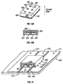
- Figure 10 shows a bottom view of a MOSFET device 80 having a generally square array of thirty-six (36) interconnect elements, comprising seventeen (17) drain interconnect elements (labeled “D” in the drawing) and seventeen (17) source interconnect elements (labeled "S” in the drawing).
- One interconnect element, labeled “G” in Figure 10 is a common gate connection; another interconnection element, labeled "X” in Figure 10, is a drain cell connection within the MOSFET as is known in the art.
- the interconnect elements, D, S, G and X are fusible solder balls (e.g., eutectic tin-lead solder balls, 0.0146 inch (0.37 mm) in diameter) which are spaced apart on a 0.5mm pitch (i.e., the dimensions labeled "A" in the drawing).
- the drain and source connections are arranged in an alternating pattern of the kind shown in Fig. 2, in which the source balls (S, Fig. 10) and the drain balls (D, Fig. 10) alternate within rows and columns that are generally parallel to the edges of the die.
- FIG 11 is an exploded view showing the spatial relationships between a flip-chip assembly comprising a MOSFET device 80 and a printed circuit board 106 onto which the MOSFET device is mounted.
- the MOSFET device 80 is of the kind shown in Figure 10.
- the drain and source solder balls 82a and 83a shown in the top comers in Figure 10, appear in the front row of contacts in the view of the MOSFET device 80 in Figure 11.
- the printed circuit board 106 comprises three layers of copper etch: a bottom layer 91, nominally 0.0028 inch (0.071 mm) thick; a middle layer 89, nominally 0.0022 inch (0.056 mm) thick; and a top layer 87, nominally 0.0018 inch (0.046 mm) thick.
- a bottom layer 91 nominally 0.0028 inch (0.071 mm) thick
- a middle layer 89 nominally 0.0022 inch (0.056 mm) thick
- a top layer 87 nominally 0.0018 inch (0.046 mm) thick.
- the top layer 87 and the middle layer 89 are separated by an insulating core 102
- the middle layer 89 and the bottom layer 91 are separated by another insulating core 104.
- Each insulating core 102 and 104 is nominally 0.004 inch (0.102 mm) thick and may, e.g., comprise a type 4000-13 laminate manufactured by New England Laminating Company, Inc., Newburgh, NY, USA.
- a layer of solder mask 85 overlays the top surface of top layer 87.
- the top layer 87 of the printed circuit board 106 comprises seventeen (17) pad-defined connections for FET drains, which may be characterized as defining laterally non-conductive regions, each drain pad 90 (two of which are shown in Figure 11) being 0.012 inch (0.305 mm) in diameter.
- the top layer 87 also comprises seventeen (17) solder-mask-defined connections for FET sources, each also 0.012 inch (0.30 mm) in diameter. The locations of two connections are shown in Figure 11 by circles 94.
- a 0.005 inch (0.127 mm) clearance region 92 separates the drain pads 90 from the remainder of the top layer 87.
- the solder mask layer 85 comprises seventeen (17) cleared-away regions above the circles 94 (two of which are shown in Figure 11 as source clearance holes 86), each 0.012 inch (0.305 mm) in diameter, and seventeen (17) cleared-away regions, each 0.017 inch (0.432 mm) in diameter, conforming to the locations of the circumferences of the clearance regions 92 (two of which are shown in Figure 11 as drain clearance holes 88).
- the top and middle layers 87 and 89 (exclusive of drain pads 90 and 99 and their associated clearance regions 92 and 98) and columns 97, form the source terminal of the MOSFET device 80.
- the bottom layer 91 with its associated columns 96 and 100 and pads 90 and 99, form the drain terminal.
- the aggregate resistance of such a construction comprising the series resistance of the source and drain terminals, each terminal extending to 3 sides of the MOSFET, and including the fusible solder ball contacts on the MOSFET device 80, but not including any other portion of the MOSFET device, is approximately 200 micro-Ohm. This interconnect resistance is substantially lower than the interconnect resistance of interconnect structures, such as in Figure 5.
- Terminating the MOSFET using all four of its sides can result in an interconnect resistance equal to or less than about 200 micro-Ohm; terminating the MOSFET using two of its sides can result in an interconnect resistance higher than about 200 micro-Ohm.
- the copper columns may be formed by the following process: a pattern of holes is etched into a first copper layer of a circuit board laminate (the laminate comprising first and second layers of copper on the two outer surfaces of a non-conductive core) to expose the surface of the non-conductive core at each etched location; a laser drills apertures at each etched location, the apertures extending through the core all the way to the inner surface of the second copper layer (the aperture will not typically go through the second copper layer owing to reflection of the laser beam by the copper); the inner surfaces of the apertures are plated up to form a hollow copper cylinder.
- the substrate 106 of Figure 12 may comprise two laminates, a first laminate comprising top layer 87, core 102, and first inner layer 89a, and a second laminate comprising bottom layer 91, core 104, and second inner layer 89b.
- Columns 96 can be formed by first etching a pattern of holes into top layer 87, the diameter of the holes conforming to the outer diameter of the columns 96; laser-drilling the core 102 at each hole location to form apertures having the diameter of columns 96, the apertures extending down to the inner surface 108 of first inner layer 89a; and plating the inside surfaces of the apertures to form columns 96.
- Each column comprises a hollow region 30a.
- Columns 100 are formed by an identical process, the columns extending through core 104 to the inside surface of inner layer 89b. The first and second laminates are then joined together to form substrate 106.
- the alternating patterns described and depicted above may be altered to accommodate various types and configurations of interconnects.
- the checkerboard-like pattern shown in FIG. 2 may be altered such that the repeating cell includes more than five balls, such that the repeating cellular pattern is internally asymmetric about one or more axes, etc.
- Various types of interconnects may be used, including but not limited to metal solder, conductive epoxy, wires, or stud bumps. Multiple interconnect layers may be used to mount a die or other circuit on to the substrate.
- the substrate can be a ceramic plate, printed circuit board, or any other substrate adapted to interconnect a circuit element.
- the circuit mounted to the substrate can be disposed on a die, another printed circuit board, or any other suitable substrate.
- the circuit element need not be lateral or vertical power MOSFET device, but rather can be any device having patterns of interconnect elements requiring a low resistance substrate interconnect.
- the insulating and conductive layers may include only traces; alternately, the layers may substantially cover a surface area of the substrate.
- the conductive layers can be formed of any suitable conductive or semiconductive material, including copper, aluminum, polysilicon, and polysalide.
- the masks discussed herein may likewise be formed of any suitable insulating material, or they may be omitted entirely in certain embodiments.
- the conductive columns may be replaced with any suitable connector which spans, alone or in cooperation with other elements, the distance between the interconnect elements (such as solder balls) and a conductive layer. Any desired number of multiple-conductive-layer substrate or substrate sections may be used, which may be advantageous to further reduce Rds-on. Any number of conductive layers may have common termination.
Landscapes
- Physics & Mathematics (AREA)
- Electromagnetism (AREA)
- Engineering & Computer Science (AREA)
- Microelectronics & Electronic Packaging (AREA)
- Insulated Gate Type Field-Effect Transistor (AREA)
- Wire Bonding (AREA)
- Structure Of Printed Boards (AREA)
Applications Claiming Priority (2)
| Application Number | Priority Date | Filing Date | Title |
|---|---|---|---|
| US10/331,032 US7038917B2 (en) | 2002-12-27 | 2002-12-27 | Low loss, high density array interconnection |
| US331032 | 2002-12-27 |
Publications (2)
| Publication Number | Publication Date |
|---|---|
| EP1439581A2 true EP1439581A2 (de) | 2004-07-21 |
| EP1439581A3 EP1439581A3 (de) | 2005-11-02 |
Family
ID=32594761
Family Applications (1)
| Application Number | Title | Priority Date | Filing Date |
|---|---|---|---|
| EP03258223A Withdrawn EP1439581A3 (de) | 2002-12-27 | 2003-12-29 | Verbindungsstruktur |
Country Status (3)
| Country | Link |
|---|---|
| US (1) | US7038917B2 (de) |
| EP (1) | EP1439581A3 (de) |
| JP (1) | JP2004214646A (de) |
Cited By (4)
| Publication number | Priority date | Publication date | Assignee | Title |
|---|---|---|---|---|
| EP1814371A1 (de) * | 2006-01-26 | 2007-08-01 | Pace Micro Technology PLC | Leiterplatte und Verwendungsverfahren dafür |
| WO2007076020A3 (en) * | 2005-12-22 | 2008-06-05 | Atmel Corp | Method and system for increasing circuitry interconnection and component capacity in a multi-component package |
| US8237266B2 (en) | 2005-12-20 | 2012-08-07 | Atmel Corporation | Component stacking for integrated circuit electronic package |
| RU2484607C2 (ru) * | 2007-01-31 | 2013-06-10 | Испано Сюиза | Электронная плата с встроенным нагревательным сопротивлением |
Families Citing this family (26)
| Publication number | Priority date | Publication date | Assignee | Title |
|---|---|---|---|---|
| US20040252491A1 (en) * | 2003-06-10 | 2004-12-16 | Armament Systems And Procedures, Inc. | Printed circuit board lamp |
| KR20060008021A (ko) * | 2004-07-23 | 2006-01-26 | 삼성전자주식회사 | 인쇄회로기판 및 이를 이용한 평판표시장치 |
| JP4421528B2 (ja) * | 2005-07-28 | 2010-02-24 | シャープ株式会社 | 半田付け実装構造およびその製造方法、並びにその利用 |
| US7838977B2 (en) * | 2005-09-07 | 2010-11-23 | Alpha & Omega Semiconductor, Ltd. | Packages for electronic devices implemented with laminated board with a top and a bottom patterned metal layers |
| US7768075B2 (en) * | 2006-04-06 | 2010-08-03 | Fairchild Semiconductor Corporation | Semiconductor die packages using thin dies and metal substrates |
| JP5175482B2 (ja) * | 2007-03-29 | 2013-04-03 | ルネサスエレクトロニクス株式会社 | 半導体装置 |
| US9070670B2 (en) * | 2009-01-29 | 2015-06-30 | International Rectifier Corporation | Electrical connectivity of die to a host substrate |
| US9818857B2 (en) | 2009-08-04 | 2017-11-14 | Gan Systems Inc. | Fault tolerant design for large area nitride semiconductor devices |
| US9029866B2 (en) | 2009-08-04 | 2015-05-12 | Gan Systems Inc. | Gallium nitride power devices using island topography |
| US8375349B2 (en) * | 2009-09-02 | 2013-02-12 | Taiwan Semiconductor Manufacturing Company, Ltd. | Method for constant power density scaling |
| US8148823B1 (en) * | 2009-12-14 | 2012-04-03 | Picor Corporation | Low loss package for electronic device |
| US20120032337A1 (en) * | 2010-08-06 | 2012-02-09 | Taiwan Semiconductor Manufacturing Company, Ltd. | Flip Chip Substrate Package Assembly and Process for Making Same |
| US9093433B2 (en) * | 2010-11-18 | 2015-07-28 | Microchip Technology Incorporated | Using bump bonding to distribute current flow on a semiconductor power device |
| US8624392B2 (en) | 2011-06-03 | 2014-01-07 | Taiwan Semiconductor Manufacturing Company, Ltd. | Electrical connection for chip scale packaging |
| DE112012004185T5 (de) * | 2011-10-07 | 2014-06-26 | Volterra Semiconductor Corp. | Leistungsmanagements-Anwendungen von Zwischenverbindungssubstraten |
| US8912668B2 (en) | 2012-03-01 | 2014-12-16 | Taiwan Semiconductor Manufacturing Company, Ltd. | Electrical connections for chip scale packaging |
| US9548281B2 (en) | 2011-10-07 | 2017-01-17 | Taiwan Semiconductor Manufacturing Company, Ltd. | Electrical connection for chip scale packaging |
| US9196573B2 (en) | 2012-07-31 | 2015-11-24 | Taiwan Semiconductor Manufacturing Company, Ltd. | Bump on pad (BOP) bonding structure |
| US8829673B2 (en) | 2012-08-17 | 2014-09-09 | Taiwan Semiconductor Manufacturing Company, Ltd. | Bonded structures for package and substrate |
| US9673161B2 (en) | 2012-08-17 | 2017-06-06 | Taiwan Semiconductor Manufacturing Company, Ltd. | Bonded structures for package and substrate |
| US9113555B2 (en) * | 2012-12-21 | 2015-08-18 | Intel Corporation | Apparatus for differential far-end crosstalk reduction |
| US8975694B1 (en) * | 2013-03-07 | 2015-03-10 | Vlt, Inc. | Low resistance power switching device |
| USD721047S1 (en) | 2013-03-07 | 2015-01-13 | Vlt, Inc. | Semiconductor device |
| KR101616625B1 (ko) * | 2014-07-30 | 2016-04-28 | 삼성전기주식회사 | 반도체 패키지 및 그 제조방법 |
| JP6741456B2 (ja) * | 2016-03-31 | 2020-08-19 | Fdk株式会社 | 多層回路基板 |
| DE102017108172B4 (de) * | 2017-04-18 | 2022-01-13 | Infineon Technologies Austria Ag | SMD-Package und Verfahren zur Herstellung eines SMD-Packages |
Family Cites Families (74)
| Publication number | Priority date | Publication date | Assignee | Title |
|---|---|---|---|---|
| US4630357A (en) | 1985-08-02 | 1986-12-23 | Ncr Corporation | Method for forming improved contacts between interconnect layers of an integrated circuit |
| US4821007A (en) | 1987-02-06 | 1989-04-11 | Tektronix, Inc. | Strip line circuit component and method of manufacture |
| JPH02163960A (ja) | 1988-12-16 | 1990-06-25 | Toshiba Corp | 半導体装置 |
| US4943539A (en) | 1989-05-09 | 1990-07-24 | Motorola, Inc. | Process for making a multilayer metallization structure |
| US5070391A (en) | 1989-11-30 | 1991-12-03 | Sgs-Thomson Microelectronics, Inc. | Semiconductor contact via structure and method |
| US5158910A (en) | 1990-08-13 | 1992-10-27 | Motorola Inc. | Process for forming a contact structure |
| JP2609753B2 (ja) | 1990-10-17 | 1997-05-14 | 株式会社東芝 | 半導体装置 |
| US5266912A (en) * | 1992-08-19 | 1993-11-30 | Micron Technology, Inc. | Inherently impedance matched multiple integrated circuit module |
| US5365082A (en) | 1992-09-30 | 1994-11-15 | Texas Instruments Incorporated | MOSFET cell array |
| JP2611615B2 (ja) | 1992-12-15 | 1997-05-21 | 日本電気株式会社 | 半導体装置の製造方法 |
| US5412239A (en) * | 1993-05-14 | 1995-05-02 | Siliconix Incorporated | Contact geometry for improved lateral MOSFET |
| US5391517A (en) | 1993-09-13 | 1995-02-21 | Motorola Inc. | Process for forming copper interconnect structure |
| US5510747A (en) | 1993-11-30 | 1996-04-23 | Siliconix Incorporated | Gate drive technique for a bidirectional blocking lateral MOSFET |
| US5442235A (en) | 1993-12-23 | 1995-08-15 | Motorola Inc. | Semiconductor device having an improved metal interconnect structure |
| US5477082A (en) | 1994-01-11 | 1995-12-19 | Exponential Technology, Inc. | Bi-planar multi-chip module |
| US5429989A (en) | 1994-02-03 | 1995-07-04 | Motorola, Inc. | Process for fabricating a metallization structure in a semiconductor device |
| US6429113B1 (en) | 1994-04-26 | 2002-08-06 | International Business Machines Corporation | Method for connecting an electrical device to a circuit substrate |
| US5476817A (en) | 1994-05-31 | 1995-12-19 | Texas Instruments Incorporated | Method of making reliable metal leads in high speed LSI semiconductors using both dummy leads and thermoconductive layers |
| US5817546A (en) | 1994-06-23 | 1998-10-06 | Stmicroelectronics S.R.L. | Process of making a MOS-technology power device |
| JPH0897411A (ja) | 1994-09-21 | 1996-04-12 | Fuji Electric Co Ltd | 横型高耐圧トレンチmosfetおよびその製造方法 |
| US5903469A (en) | 1994-11-08 | 1999-05-11 | Synopsys, Inc. | Method of extracting layout parasitics for nets of an integrated circuit using a connectivity-based approach |
| US5869371A (en) | 1995-06-07 | 1999-02-09 | Stmicroelectronics, Inc. | Structure and process for reducing the on-resistance of mos-gated power devices |
| US5756395A (en) | 1995-08-18 | 1998-05-26 | Lsi Logic Corporation | Process for forming metal interconnect structures for use with integrated circuit devices to form integrated circuit structures |
| US5633199A (en) | 1995-11-02 | 1997-05-27 | Motorola Inc. | Process for fabricating a metallized interconnect structure in a semiconductor device |
| US6228719B1 (en) | 1995-11-06 | 2001-05-08 | Stmicroelectronics S.R.L. | MOS technology power device with low output resistance and low capacitance, and related manufacturing process |
| JP3457123B2 (ja) | 1995-12-07 | 2003-10-14 | 株式会社リコー | 半導体装置 |
| US5578841A (en) | 1995-12-18 | 1996-11-26 | Motorola, Inc. | Vertical MOSFET device having frontside and backside contacts |
| US5796671A (en) | 1996-03-01 | 1998-08-18 | Wahlstrom; Sven E. | Dynamic random access memory |
| US5710451A (en) | 1996-04-10 | 1998-01-20 | Philips Electronics North America Corporation | High-voltage lateral MOSFET SOI device having a semiconductor linkup region |
| DE19617055C1 (de) * | 1996-04-29 | 1997-06-26 | Semikron Elektronik Gmbh | Halbleiterleistungsmodul hoher Packungsdichte in Mehrschichtbauweise |
| US5777383A (en) | 1996-05-09 | 1998-07-07 | Lsi Logic Corporation | Semiconductor chip package with interconnect layers and routing and testing methods |
| US5710455A (en) | 1996-07-29 | 1998-01-20 | Motorola | Lateral MOSFET with modified field plates and damage areas |
| JPH10163317A (ja) | 1996-11-28 | 1998-06-19 | Mitsubishi Electric Corp | 半導体装置及びその製造方法 |
| US5856636A (en) * | 1997-03-03 | 1999-01-05 | Sanso; David W. | Electronic circuit prototype wiring board with visually distinctive contact pads |
| US6395629B1 (en) | 1997-04-16 | 2002-05-28 | Stmicroelectronics, Inc. | Interconnect method and structure for semiconductor devices |
| JPH10303562A (ja) * | 1997-04-30 | 1998-11-13 | Toshiba Corp | プリント配線板 |
| US6277728B1 (en) | 1997-06-13 | 2001-08-21 | Micron Technology, Inc. | Multilevel interconnect structure with low-k dielectric and method of fabricating the structure |
| US5891756A (en) | 1997-06-27 | 1999-04-06 | Delco Electronics Corporation | Process for converting a wire bond pad to a flip chip solder bump pad and pad formed thereby |
| US6005271A (en) | 1997-11-05 | 1999-12-21 | Magepower Semiconductor Corp. | Semiconductor cell array with high packing density |
| US6127233A (en) | 1997-12-05 | 2000-10-03 | Texas Instruments Incorporated | Lateral MOSFET having a barrier between the source/drain regions and the channel region |
| US5898217A (en) | 1998-01-05 | 1999-04-27 | Motorola, Inc. | Semiconductor device including a substrate having clustered interconnects |
| US6105852A (en) | 1998-02-05 | 2000-08-22 | International Business Machines Corporation | Etched glass solder bump transfer for flip chip integrated circuit devices |
| US6373100B1 (en) | 1998-03-04 | 2002-04-16 | Semiconductor Components Industries Llc | Semiconductor device and method for fabricating the same |
| US6358837B1 (en) | 1998-03-31 | 2002-03-19 | Lsi Logic Corporation | Method of electrically connecting and isolating components with vertical elements extending between interconnect layers in an integrated circuit |
| US6251740B1 (en) | 1998-12-23 | 2001-06-26 | Lsi Logic Corporation | Method of forming and electrically connecting a vertical interdigitated metal-insulator-metal capacitor extending between interconnect layers in an integrated circuit |
| US6108210A (en) * | 1998-04-24 | 2000-08-22 | Amerasia International Technology, Inc. | Flip chip devices with flexible conductive adhesive |
| US6239491B1 (en) | 1998-05-18 | 2001-05-29 | Lsi Logic Corporation | Integrated circuit structure with thin dielectric between at least local interconnect level and first metal interconnect level, and process for making same |
| US6423623B1 (en) | 1998-06-09 | 2002-07-23 | Fairchild Semiconductor Corporation | Low Resistance package for semiconductor devices |
| US6193143B1 (en) | 1998-08-05 | 2001-02-27 | Matsushita Electric Industrial Co., Ltd. | Solder bump forming method and mounting apparatus and mounting method of solder ball |
| JP4079522B2 (ja) | 1998-08-27 | 2008-04-23 | エルピーダメモリ株式会社 | 半導体集積回路装置 |
| JP3565047B2 (ja) | 1998-10-07 | 2004-09-15 | 松下電器産業株式会社 | 半田バンプの形成方法および半田バンプの実装方法 |
| US6124627A (en) | 1998-12-03 | 2000-09-26 | Texas Instruments Incorporated | Lateral MOSFET having a barrier between the source/drain region and the channel region using a heterostructure raised source/drain region |
| EP1017087A1 (de) | 1998-12-29 | 2000-07-05 | STMicroelectronics S.r.l. | Herstellungsverfahren für einen halbleitersubstratintegrierten MOS-Transistor |
| US6075293A (en) | 1999-03-05 | 2000-06-13 | Advanced Micro Devices, Inc. | Semiconductor device having a multi-layer metal interconnect structure |
| US6251501B1 (en) | 1999-03-29 | 2001-06-26 | Delphi Technologies, Inc. | Surface mount circuit device and solder bumping method therefor |
| JP3066963B1 (ja) | 1999-03-31 | 2000-07-17 | インターナショナル・ビジネス・マシーンズ・コーポレ−ション | はんだバンプの成形方法及び成形装置 |
| JP2000349198A (ja) | 1999-04-02 | 2000-12-15 | Nitto Denko Corp | チップサイズパッケージ用インターポーザ及びその製造方法と中間部材 |
| EP1043778A1 (de) | 1999-04-06 | 2000-10-11 | STMicroelectronics S.r.l. | Verfahren zur Herstellung eines Hochspannungs-MOS-Feldeffekttransistors |
| JP2000294545A (ja) | 1999-04-09 | 2000-10-20 | Nec Corp | 半導体装置及びその製造方法 |
| US6221693B1 (en) | 1999-06-14 | 2001-04-24 | Thin Film Module, Inc. | High density flip chip BGA |
| US6392428B1 (en) | 1999-11-16 | 2002-05-21 | Eaglestone Partners I, Llc | Wafer level interposer |
| EP1104022A1 (de) | 1999-11-29 | 2001-05-30 | STMicroelectronics S.r.l. | Herstellungsverfahren eines integrierten Schaltkreis der Hoch- und Niederspannungs-MOS-Transistoren sowie EPROM-Zellen beinhaltet |
| JP2001203470A (ja) | 2000-01-21 | 2001-07-27 | Toshiba Corp | 配線基板、半導体パッケージ、および半導体装置 |
| US6278264B1 (en) | 2000-02-04 | 2001-08-21 | Volterra Semiconductor Corporation | Flip-chip switching regulator |
| WO2001059842A1 (en) | 2000-02-10 | 2001-08-16 | International Rectifier Corporation | Vertical conduction flip-chip device with bump contacts on single surface |
| JP2001259961A (ja) * | 2000-03-15 | 2001-09-25 | Disco Abrasive Syst Ltd | 加工装置 |
| US6392290B1 (en) | 2000-04-07 | 2002-05-21 | Siliconix Incorporated | Vertical structure for semiconductor wafer-level chip scale packages |
| EP1160873A1 (de) | 2000-05-19 | 2001-12-05 | STMicroelectronics S.r.l. | MOS-Technologie-Leistungsanordnung |
| JP4979154B2 (ja) | 2000-06-07 | 2012-07-18 | ルネサスエレクトロニクス株式会社 | 半導体装置 |
| US6313007B1 (en) | 2000-06-07 | 2001-11-06 | Agere Systems Guardian Corp. | Semiconductor device, trench isolation structure and methods of formations |
| US6710441B2 (en) | 2000-07-13 | 2004-03-23 | Isothermal Research Systems, Inc. | Power semiconductor switching devices, power converters, integrated circuit assemblies, integrated circuitry, power current switching methods, methods of forming a power semiconductor switching device, power conversion methods, power semiconductor switching device packaging methods, and methods of forming a power transistor |
| JP2002353588A (ja) * | 2001-05-29 | 2002-12-06 | Mitsubishi Electric Corp | 配線基板及び配線基板の製造方法 |
| US6521842B2 (en) * | 2001-06-20 | 2003-02-18 | International Business Machines Corporation | Hybrid surface mount and pin thru hole circuit board |
| US6747216B2 (en) * | 2002-02-04 | 2004-06-08 | Intel Corporation | Power-ground plane partitioning and via connection to utilize channel/trenches for power delivery |
-
2002
- 2002-12-27 US US10/331,032 patent/US7038917B2/en not_active Expired - Lifetime
-
2003
- 2003-12-18 JP JP2003420364A patent/JP2004214646A/ja active Pending
- 2003-12-29 EP EP03258223A patent/EP1439581A3/de not_active Withdrawn
Cited By (6)
| Publication number | Priority date | Publication date | Assignee | Title |
|---|---|---|---|---|
| US8237266B2 (en) | 2005-12-20 | 2012-08-07 | Atmel Corporation | Component stacking for integrated circuit electronic package |
| US8525329B2 (en) | 2005-12-20 | 2013-09-03 | Atmel Corporation | Component stacking for integrated circuit electronic package |
| WO2007076020A3 (en) * | 2005-12-22 | 2008-06-05 | Atmel Corp | Method and system for increasing circuitry interconnection and component capacity in a multi-component package |
| US7821122B2 (en) | 2005-12-22 | 2010-10-26 | Atmel Corporation | Method and system for increasing circuitry interconnection and component capacity in a multi-component package |
| EP1814371A1 (de) * | 2006-01-26 | 2007-08-01 | Pace Micro Technology PLC | Leiterplatte und Verwendungsverfahren dafür |
| RU2484607C2 (ru) * | 2007-01-31 | 2013-06-10 | Испано Сюиза | Электронная плата с встроенным нагревательным сопротивлением |
Also Published As
| Publication number | Publication date |
|---|---|
| US7038917B2 (en) | 2006-05-02 |
| US20040125577A1 (en) | 2004-07-01 |
| JP2004214646A (ja) | 2004-07-29 |
| EP1439581A3 (de) | 2005-11-02 |
Similar Documents
| Publication | Publication Date | Title |
|---|---|---|
| US7038917B2 (en) | Low loss, high density array interconnection | |
| US6818977B2 (en) | Semiconductor devices and semiconductor device components with peripherally located, castellated contacts, assemblies and packages including such semiconductor devices or packages | |
| US5942795A (en) | Leaded substrate carrier for integrated circuit device and leaded substrate carrier device assembly | |
| CN102487021B (zh) | 形成用于倒装半导体管芯的焊盘布局的半导体器件和方法 | |
| US9117815B2 (en) | Method of fabricating a packaged semiconductor | |
| US7479705B2 (en) | Semiconductor device | |
| EP0080041A2 (de) | Verbindungsanordnungen für elektrische Schaltungen | |
| US20020060361A1 (en) | Semiconductor package for three-dimensional mounting, fabrication method thereof , and semiconductor device | |
| EP1076915A1 (de) | Chipstapel und seine herstellung | |
| KR20100087329A (ko) | 칩 스케일 적층형 다이 패키지 | |
| US10128221B2 (en) | Package assembly having interconnect for stacked electronic devices and method for manufacturing the same | |
| EP1570496B1 (de) | Bauelement aus leitendem polymer und verfahren zu seiner herstellung | |
| US9324633B2 (en) | Multi-level package assembly having conductive vias coupled to chip carrier for each level and method for manufacturing the same | |
| US9379071B2 (en) | Single inline no-lead semiconductor package | |
| JP3927783B2 (ja) | 半導体部品 | |
| US8354744B2 (en) | Stacked semiconductor package having reduced height | |
| KR100634238B1 (ko) | 테이프 캐리어 패키지용 탭 테이프 | |
| US20060055501A1 (en) | Conductive polymer device and method of manufacturing same | |
| US5946195A (en) | Semiconductor device, method of making the same and mounting the same, circuit board and flexible substrate | |
| US20070096271A1 (en) | Substrate frame | |
| US8148823B1 (en) | Low loss package for electronic device | |
| EP1154479A2 (de) | Mehrzeiliger Raster für Gehäusungs- und Testanwendung | |
| US20130068516A1 (en) | High io substrates and interposers without vias | |
| JP2935356B2 (ja) | 半導体装置および基板ならびに半導体装置の実装構造 | |
| JP2004253518A (ja) | 半導体装置及び半導体装置の製造方法 |
Legal Events
| Date | Code | Title | Description |
|---|---|---|---|
| PUAI | Public reference made under article 153(3) epc to a published international application that has entered the european phase |
Free format text: ORIGINAL CODE: 0009012 |
|
| AK | Designated contracting states |
Kind code of ref document: A2 Designated state(s): AT BE BG CH CY CZ DE DK EE ES FI FR GB GR HU IE IT LI LU MC NL PT RO SE SI SK TR |
|
| AX | Request for extension of the european patent |
Extension state: AL LT LV MK |
|
| RAP1 | Party data changed (applicant data changed or rights of an application transferred) |
Owner name: VLT, INC. |
|
| PUAL | Search report despatched |
Free format text: ORIGINAL CODE: 0009013 |
|
| AK | Designated contracting states |
Kind code of ref document: A3 Designated state(s): AT BE BG CH CY CZ DE DK EE ES FI FR GB GR HU IE IT LI LU MC NL PT RO SE SI SK TR |
|
| AX | Request for extension of the european patent |
Extension state: AL LT LV MK |
|
| AKX | Designation fees paid | ||
| REG | Reference to a national code |
Ref country code: DE Ref legal event code: 8566 |
|
| STAA | Information on the status of an ep patent application or granted ep patent |
Free format text: STATUS: THE APPLICATION IS DEEMED TO BE WITHDRAWN |
|
| 18D | Application deemed to be withdrawn |
Effective date: 20060503 |