EP1428677B1 - Druckplatte, leiterplatte und verfahren zum drucken einer leiterplatte - Google Patents
Druckplatte, leiterplatte und verfahren zum drucken einer leiterplatte Download PDFInfo
- Publication number
- EP1428677B1 EP1428677B1 EP03787306A EP03787306A EP1428677B1 EP 1428677 B1 EP1428677 B1 EP 1428677B1 EP 03787306 A EP03787306 A EP 03787306A EP 03787306 A EP03787306 A EP 03787306A EP 1428677 B1 EP1428677 B1 EP 1428677B1
- Authority
- EP
- European Patent Office
- Prior art keywords
- squeegee
- printing plate
- projection
- paste
- printing
- Prior art date
- Legal status (The legal status is an assumption and is not a legal conclusion. Google has not performed a legal analysis and makes no representation as to the accuracy of the status listed.)
- Expired - Lifetime
Links
- 238000000034 method Methods 0.000 title claims abstract description 45
- 239000002184 metal Substances 0.000 claims abstract description 26
- 229910052751 metal Inorganic materials 0.000 claims abstract description 26
- 239000000463 material Substances 0.000 claims description 18
- 238000005530 etching Methods 0.000 claims description 5
- 238000000465 moulding Methods 0.000 claims description 3
- 238000004140 cleaning Methods 0.000 abstract description 33
- 238000004519 manufacturing process Methods 0.000 description 12
- 238000003754 machining Methods 0.000 description 7
- 230000002411 adverse Effects 0.000 description 6
- 239000004760 aramid Substances 0.000 description 6
- 238000005429 filling process Methods 0.000 description 6
- 229920005989 resin Polymers 0.000 description 6
- 239000011347 resin Substances 0.000 description 6
- 239000004744 fabric Substances 0.000 description 5
- 239000011888 foil Substances 0.000 description 5
- 229920006231 aramid fiber Polymers 0.000 description 4
- 238000012790 confirmation Methods 0.000 description 4
- 230000000694 effects Effects 0.000 description 4
- 239000003822 epoxy resin Substances 0.000 description 3
- 239000011295 pitch Substances 0.000 description 3
- 229920000647 polyepoxide Polymers 0.000 description 3
- 230000000717 retained effect Effects 0.000 description 3
- 229920001187 thermosetting polymer Polymers 0.000 description 3
- RYGMFSIKBFXOCR-UHFFFAOYSA-N Copper Chemical compound [Cu] RYGMFSIKBFXOCR-UHFFFAOYSA-N 0.000 description 2
- 239000000853 adhesive Substances 0.000 description 2
- 230000001070 adhesive effect Effects 0.000 description 2
- 229920003235 aromatic polyamide Polymers 0.000 description 2
- 239000002131 composite material Substances 0.000 description 2
- 229910052802 copper Inorganic materials 0.000 description 2
- 239000010949 copper Substances 0.000 description 2
- 238000005520 cutting process Methods 0.000 description 2
- 239000000835 fiber Substances 0.000 description 2
- 239000003365 glass fiber Substances 0.000 description 2
- 238000004806 packaging method and process Methods 0.000 description 2
- -1 polyethylene terephthalate Polymers 0.000 description 2
- 229920000139 polyethylene terephthalate Polymers 0.000 description 2
- 239000005020 polyethylene terephthalate Substances 0.000 description 2
- 238000002360 preparation method Methods 0.000 description 2
- 229910001220 stainless steel Inorganic materials 0.000 description 2
- 239000010935 stainless steel Substances 0.000 description 2
- 230000006835 compression Effects 0.000 description 1
- 238000007906 compression Methods 0.000 description 1
- 230000002844 continuous effect Effects 0.000 description 1
- 238000007796 conventional method Methods 0.000 description 1
- 230000007423 decrease Effects 0.000 description 1
- 238000005304 joining Methods 0.000 description 1
- 238000010030 laminating Methods 0.000 description 1
- 239000000155 melt Substances 0.000 description 1
- 238000000059 patterning Methods 0.000 description 1
- 230000000704 physical effect Effects 0.000 description 1
- 239000002985 plastic film Substances 0.000 description 1
- 229920006255 plastic film Polymers 0.000 description 1
- 229920003225 polyurethane elastomer Polymers 0.000 description 1
- 238000005096 rolling process Methods 0.000 description 1
- 238000005549 size reduction Methods 0.000 description 1
- 238000010408 sweeping Methods 0.000 description 1
- 239000002759 woven fabric Substances 0.000 description 1
Images


Classifications
-
- H—ELECTRICITY
- H05—ELECTRIC TECHNIQUES NOT OTHERWISE PROVIDED FOR
- H05K—PRINTED CIRCUITS; CASINGS OR CONSTRUCTIONAL DETAILS OF ELECTRIC APPARATUS; MANUFACTURE OF ASSEMBLAGES OF ELECTRICAL COMPONENTS
- H05K3/00—Apparatus or processes for manufacturing printed circuits
- H05K3/10—Apparatus or processes for manufacturing printed circuits in which conductive material is applied to the insulating support in such a manner as to form the desired conductive pattern
- H05K3/12—Apparatus or processes for manufacturing printed circuits in which conductive material is applied to the insulating support in such a manner as to form the desired conductive pattern using thick film techniques, e.g. printing techniques to apply the conductive material or similar techniques for applying conductive paste or ink patterns
- H05K3/1216—Apparatus or processes for manufacturing printed circuits in which conductive material is applied to the insulating support in such a manner as to form the desired conductive pattern using thick film techniques, e.g. printing techniques to apply the conductive material or similar techniques for applying conductive paste or ink patterns by screen printing or stencil printing
- H05K3/1225—Screens or stencils; Holders therefor
-
- B—PERFORMING OPERATIONS; TRANSPORTING
- B41—PRINTING; LINING MACHINES; TYPEWRITERS; STAMPS
- B41F—PRINTING MACHINES OR PRESSES
- B41F15/00—Screen printers
- B41F15/14—Details
- B41F15/34—Screens, Frames; Holders therefor
- B41F15/36—Screens, Frames; Holders therefor flat
-
- B—PERFORMING OPERATIONS; TRANSPORTING
- B41—PRINTING; LINING MACHINES; TYPEWRITERS; STAMPS
- B41F—PRINTING MACHINES OR PRESSES
- B41F35/00—Cleaning arrangements or devices
- B41F35/003—Cleaning arrangements or devices for screen printers or parts thereof
-
- B—PERFORMING OPERATIONS; TRANSPORTING
- B41—PRINTING; LINING MACHINES; TYPEWRITERS; STAMPS
- B41M—PRINTING, DUPLICATING, MARKING, OR COPYING PROCESSES; COLOUR PRINTING
- B41M1/00—Inking and printing with a printer's forme
- B41M1/12—Stencil printing; Silk-screen printing
-
- B—PERFORMING OPERATIONS; TRANSPORTING
- B41—PRINTING; LINING MACHINES; TYPEWRITERS; STAMPS
- B41N—PRINTING PLATES OR FOILS; MATERIALS FOR SURFACES USED IN PRINTING MACHINES FOR PRINTING, INKING, DAMPING, OR THE LIKE; PREPARING SUCH SURFACES FOR USE AND CONSERVING THEM
- B41N1/00—Printing plates or foils; Materials therefor
- B41N1/24—Stencils; Stencil materials; Carriers therefor
- B41N1/248—Mechanical details, e.g. fixation holes, reinforcement or guiding means; Perforation lines; Ink holding means; Visually or otherwise detectable marking means; Stencil units
-
- H—ELECTRICITY
- H05—ELECTRIC TECHNIQUES NOT OTHERWISE PROVIDED FOR
- H05K—PRINTED CIRCUITS; CASINGS OR CONSTRUCTIONAL DETAILS OF ELECTRIC APPARATUS; MANUFACTURE OF ASSEMBLAGES OF ELECTRICAL COMPONENTS
- H05K3/00—Apparatus or processes for manufacturing printed circuits
- H05K3/40—Forming printed elements for providing electric connections to or between printed circuits
- H05K3/4038—Through-connections; Vertical interconnect access [VIA] connections
- H05K3/4053—Through-connections; Vertical interconnect access [VIA] connections by thick-film techniques
-
- H—ELECTRICITY
- H05—ELECTRIC TECHNIQUES NOT OTHERWISE PROVIDED FOR
- H05K—PRINTED CIRCUITS; CASINGS OR CONSTRUCTIONAL DETAILS OF ELECTRIC APPARATUS; MANUFACTURE OF ASSEMBLAGES OF ELECTRICAL COMPONENTS
- H05K2201/00—Indexing scheme relating to printed circuits covered by H05K1/00
- H05K2201/09—Shape and layout
- H05K2201/09009—Substrate related
- H05K2201/09063—Holes or slots in insulating substrate not used for electrical connections
-
- H—ELECTRICITY
- H05—ELECTRIC TECHNIQUES NOT OTHERWISE PROVIDED FOR
- H05K—PRINTED CIRCUITS; CASINGS OR CONSTRUCTIONAL DETAILS OF ELECTRIC APPARATUS; MANUFACTURE OF ASSEMBLAGES OF ELECTRICAL COMPONENTS
- H05K2201/00—Indexing scheme relating to printed circuits covered by H05K1/00
- H05K2201/09—Shape and layout
- H05K2201/09209—Shape and layout details of conductors
- H05K2201/09654—Shape and layout details of conductors covering at least two types of conductors provided for in H05K2201/09218 - H05K2201/095
- H05K2201/09709—Staggered pads, lands or terminals; Parallel conductors in different planes
-
- H—ELECTRICITY
- H05—ELECTRIC TECHNIQUES NOT OTHERWISE PROVIDED FOR
- H05K—PRINTED CIRCUITS; CASINGS OR CONSTRUCTIONAL DETAILS OF ELECTRIC APPARATUS; MANUFACTURE OF ASSEMBLAGES OF ELECTRICAL COMPONENTS
- H05K2203/00—Indexing scheme relating to apparatus or processes for manufacturing printed circuits covered by H05K3/00
- H05K2203/01—Tools for processing; Objects used during processing
- H05K2203/0191—Using tape or non-metallic foil in a process, e.g. during filling of a hole with conductive paste
-
- H—ELECTRICITY
- H05—ELECTRIC TECHNIQUES NOT OTHERWISE PROVIDED FOR
- H05K—PRINTED CIRCUITS; CASINGS OR CONSTRUCTIONAL DETAILS OF ELECTRIC APPARATUS; MANUFACTURE OF ASSEMBLAGES OF ELECTRICAL COMPONENTS
- H05K3/00—Apparatus or processes for manufacturing printed circuits
- H05K3/0011—Working of insulating substrates or insulating layers
- H05K3/0044—Mechanical working of the substrate, e.g. drilling or punching
- H05K3/0052—Depaneling, i.e. dividing a panel into circuit boards; Working of the edges of circuit boards
-
- H—ELECTRICITY
- H05—ELECTRIC TECHNIQUES NOT OTHERWISE PROVIDED FOR
- H05K—PRINTED CIRCUITS; CASINGS OR CONSTRUCTIONAL DETAILS OF ELECTRIC APPARATUS; MANUFACTURE OF ASSEMBLAGES OF ELECTRICAL COMPONENTS
- H05K3/00—Apparatus or processes for manufacturing printed circuits
- H05K3/40—Forming printed elements for providing electric connections to or between printed circuits
- H05K3/4038—Through-connections; Vertical interconnect access [VIA] connections
- H05K3/4053—Through-connections; Vertical interconnect access [VIA] connections by thick-film techniques
- H05K3/4069—Through-connections; Vertical interconnect access [VIA] connections by thick-film techniques for via connections in organic insulating substrates
Definitions
- the present invention relates to a printing plate used for patterning and filling through holes in a two-sided, multilayered or the like printed board with a paste.
- the invention also relates to a printing method for the printed board using the printing plate.
- Fig. 13A through Fig. 13F are cross-sectional views of a printed circuit board showing the production steps in the conventional manufacturing method
- Fig. 14 a perspective view showing a plate framework of the prior art provided with a mask having an opening
- Fig. 15 a longitudinal sectional view of the same plate framework provided with the mask having the opening
- Fig. 16A through Fig. 16G cross-sectional views of a prepreg sheet showing the production steps for filling it with paste by the squeegeeing method
- Fig. 17 a cross-sectional view of a part of a printed circuit board which is being filled with paste.
- prepreg sheet 21 has a size of 300mm by 500mm and a thickness of approximately 150 ⁇ m, for example.
- Prepreg sheet 21 used here may be a board material of composite prepared by having an unwoven fabric formed of all-aromatic polyamide fibers impregnated with a thermosetting epoxy resin.
- Mask films 22a and 22b have a Si-based mold release layer formed into a thickness of 0.01 ⁇ m or less on each of their surfaces to be bonded to prepreg sheet 21.
- Each of mask films 22a and 22b has a total thickness of about 16 ⁇ m, and that a plastic film of 300mm in width made of such material as polyethylene terephthalate may be used.
- a method proposed here for adhesion between prepreg sheet 21 and mask films 22a and 22b uses a laminating apparatus which melts the resin content of prepreg sheet 21 and bonds it continuously to mask films 22a and 22b.
- Through holes 23 are filled with conductive paste 24 for making electrical connections with metal foils 25a and 25b of 35pm in thickness made of copper, for instance, placed on both surfaces of prepreg sheet 21.
- these through holes 23 are formed in predetermined locations of mask films 22a and 22b bonded to the both surfaces of prepreg sheet 21 by using laser beam machining or the like method, as shown in Fig. 13B.
- Through holes 23 are then filled with conductive paste 24 as shown in Fig. 13C.
- Filling of conductive paste 24 may be made with such a method that prepreg sheet 21 having through holes 23 is placed on stage 6 (shown in Fig. 16A to Fig. 16G, as will be described later) of an ordinary printing machine (not shown in Fig. 13), and conductive paste 24 is filled directly over mask film 22a by reciprocating alternately two squeegees made of such a material as polyurethane rubber.
- mask films 22a and 22b on prepreg sheet 21 act individually as print masks, and they also serve as means for preventing the surfaces of prepreg sheet 21 from getting contaminated.
- the squeegeeing method is used for filling of conductive paste 24. Since prepreg sheet 21 has exclusive mask films 22a and 22b, plate framework 1 of plate 10 for printing is provided with mask 2 made of an approx. 3mm thick stainless steel having opening 4 measuring 250mm by 450mm, which is larger than an effective paste-filling area of prepreg sheet 21, as shown in Fig. 14 and Fig. 15.
- prepreg sheet 21 formed with through holes 23 is placed on stage 6 of a printing machine (not shown), and mask 2 is set on top of them, as shown in Fig. 16A.
- moving-forth squeegee 8a and moving-back squeegees 8b disposed above mask 2 in a manner to move forward and backward freely and to pressurize vertically
- moving-forth squeegee 8a is lowered to a predetermined position on mask 2 and it is moved forward while pushing a drop of conductive paste 24 to roll about with a pressure.
- moving-forth squeegee 8a is advanced to pass over edge 5b of the opening of mask 2, and to reach on top of prepreg sheet 21, as shown in Fig. 16B.
- Both moving-forth squeegee 8a and moving-back squeegee 8b have the function of moving up and down freely with respect to position of prepreg sheet 21 while maintaining the pressure.
- moving-back squeegee 8b is lowered to a predetermined position on mask 2 as shown in Fig. 16D.
- moving-back squeegee 8b is moved to sweep over mask 2 and prepreg sheet 21 in the like manner as moving-forth squeegee 8a, as shown in Fig. 16E to Fig. 16G, and this completes the filling of through holes 23 with conductive paste 24.
- Prepreg sheet 21 in the above state is compressed to thickness "t2" (approx. 100pm) as shown in Fig. 13F by subjecting it to a thermal compression.
- This process also bonds metal foils 25a and 25b with prepreg sheet 21. Consequently, metal foils 25a and 25b on the both surfaces are connected electrically via conductive paste 24 filled in through holes 23 provided in the predetermined locations.
- Metal foils 25a and 25b are then etched selectively to form a prescribed circuit pattern (not shown in Fig. 13F), to obtain a two-sided printed board.
- moving-back squeegee 8b When any of the squeegees bearing conductive paste 24, especially moving-back squeegee 8b, first passes over through holes 23 formed in prepreg sheet 21, moving-back squeegee 8b tends to leave hard paste on top of these through holes 23 across the entire filling width of the paste in its moving direction. It thus gives rise to a problem that a part of conductive paste 24 transfers to mask film 22a when mask films 22a and 22b are removed, and adversely influences quality of the product.
- a printing plate, a printed board and a method of filling paste according to this invention comprise the step of removing paste of high viscosity adhering to an edge of a squeegee by moving the squeegee to pass through a squeegee cleaning section provided on the printing plate before the squeegee sweeps over a through hole of the printed board product.
- the invention can thus provide the printed board of outstanding quality.
- the printing plate of this invention has a frame-shaped opening which covers generally all or a part of the outer periphery of a circuit board material, and a metal sheet attached to each of locations on back surfaces of slanting areas and two other sides of the opening in a manner that they extend by a predetermined amount.
- At least one metal sheet attached to one of the slanting areas is provided with a projection at a predetermined location on the upper surface of the extended portion. The projection can remove paste of high viscosity built up on the edge of the squeegee when it passes over the slanting area, and avoid the hard paste from being left on the through hole of the product (printed board).
- This structure has an advantage of excluding the possibility of adverse effect to the quality due to the paste, a portion of which may be transferred to a mask film when the mask film is removed, and thereby it can provide the printing plate useful for achieving this printing method of high paste-filling quality.
- the printing method according to this invention is a method of printing paste on a material to be printed, by reciprocating the squeegee, wherein the projection on the printing plate is used to remove paste adhering to the edge of the squeegee before start of the printing.
- This method can thus remove the paste of high viscosity built up on the edge of the squeegee when it passes over the slanting area, and avoid the hard paste from being left on the through hole of the product.
- the method has an advantage of excluding the possibility of adverse effect to the quality due to the paste, a portion of which may be transferred to the mask film when the mask film is removed, and thereby it can provide the printing method for achieving high paste-filling quality.
- a printed board and a method of printing on the printed board comprise the step of forming a squeegee cleaning section in a board material having mask films on both surfaces prior to filling a through hole provided in the board material with conductive paste by the squeegeeing method, wherein the squeegee cleaning section comprises any of un-penetrated holes and through holes with raised brims formed by laser beam machining in a linear or zigzag pattern and a non-penetrated groove formed by a cutting blade into a linear or zigzag pattern located in a predetermined area in an unusable portion or the outside of a product area but within a printable space of the circuit board material.
- the cleaning section can remove the paste of high viscosity built up on the edge of the squeegee before the through hole is filled with the paste, and avoid the hard paste from being left on the through hole of the product.
- This structure thus has an advantage of excluding the possibility of adverse effect to the quality due to the paste, a portion of which may be transferred to the mask film when the mask film is removed, and thereby it can provide the printing method of achieving high paste-filling quality.
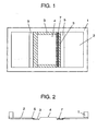
- Fig. 1 is a plan view of a printing plate according to the present invention
- Fig. 2 is a longitudinal sectional view of the printing plate of the present invention.
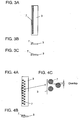
- Fig. 3A through Fig. 3C are illustrations individually showing first metal sheets according to the present, wherein Fig. 3A is a plan view and Fig. 3B and 3C are cross-sectional views of them.
- Fig. 4A through Fig. 4C are illustrations showing individually different views of a second metal sheet according to the present invention, wherein Fig. 4A is a plan view, Fig. 4B is a cross-sectional view and Fig. 4C is an enlarged plan view of the same.
- Fig. 5 shows cross-sectional views of a printed board, illustrating the production steps for filling it with paste by a squeegeeing method according to the present invention
- Fig. 6 is a cross-sectional view of a part of the printed board which is being filled with the paste by using the printing plate according to this invention.
- like reference numerals are used throughout to designate like structural elements and like components as those described in the "Background Art” section, and their detailed description is omitted.
- mask 2 made of an approx. 3mm thick stainless steel is mounted to plate framework 1.
- Mask 2 has opening 4 measuring 250mm by 450mm, for instance, which is larger than a paste-filling area of prepreg sheet 21, as shown in Fig. 1 and Fig. 2 (in this instance, exclusive mask films are disposed to prepreg sheet 21 of 300mm by 500mm and approx. 150 ⁇ m in thickness).
- Mask 2 is provided with slanting areas 5 in opening 4 at two ends intersecting a moving direction of a squeegee, i.e., the direction of two short sides of opening 4, in order to facilitate a sweeping movement of the squeegee.
- Slanting areas 5 have a slant angle set to approx. 15 degrees.
- Metal sheets 3 are fixed with adhesive or the like material to respective positions on back surfaces of the slanting areas 5 and two other sides of the opening in a manner so that they extend by approx. 5mm from the respective sides.
- Squeegee cleaning section 7 is formed at a predetermined location on the upper surface of approx. 100 ⁇ m thick metal sheet 3 extending from the back surface of slanting area 5 of mask 2.
- Squeegee cleaning section 7 comprises any of a linearly shaped projection of approx. 40 ⁇ m high as depicted in Fig. 3A to Fig. 3C and projections formed into approx. 40 ⁇ m high and 300 ⁇ m diameter with approx. 500 ⁇ m pitches in a zigzag pattern of 500 ⁇ m wide as depicted in Fig. 4A to Fig. 4C.
- the projections in squeegee cleaning section 7 were described as being approx. 40 ⁇ m high, it was confirmed that they can be 3 ⁇ m or higher to give an equivalent effectiveness. It is especially desirable that the projections have a height of 40 ⁇ m or less to avoid damages to the edge of the squeegee.
- etching or the like method it is desirable to use the etching or the like method to round edges of the projections in order to prevent the squeegee from being damaged.
- squeegee cleaning section 7 When squeegee cleaning section 7 is formed with projections of the zigzag pattern, it is especially desirable that the individual projections are arranged at such pitches that they are flash or overlap with one another as shown in Fig. 4C. Moreover, although squeegee cleaning section 7 is formed only with the projections in the first exemplary embodiment, inside of these projections may be perforated individually with a through hole or un-penetrated hole.
- moving-forth squeegee 8a and moving-back squeegees 8b disposed above mask 2 in a manner to move forward and backward freely and to pressurize vertically
- moving-forth squeegee 8a is lowered to a predetermined position on mask 2 and it is moved forward while pushing a drop of conductive paste 24 to roll about with a pressure.
- Moving-forth squeegee 8a is then advanced to pass over slanting area 5 of mask 2, and to reach on top of prepreg sheet 21, as shown in Fig. 5B.
- Both moving-forth squeegee 8a and moving-back squeegee 8b have the function of moving up and down freely while maintaining the pressure to prepreg sheet 21 according to their positions.
- moving-back squeegee 8b is moved to sweep over mask 2 and prepreg sheet 21 in the like manner as moving-forth squeegee 8a, as shown in Fig. 5E to Fig. 5G, and this completes the filling of through holes 23 with conductive paste 24.
- the printing plate is provided with metal sheets 3 extending from the back surfaces of slanting areas 5 of mask 2, and that one of metal sheets 3 located at the start side of moving-back squeegee 8b has squeegee cleaning section 7 comprised of a projection formed at a predetermined location on the upper surface thereof.
- the start side of moving-back squeegee 8b defines one side of mask 2 from which squeegee 8b begins its forward movement while rolling about the drop of conductive paste 24.
- FIG.6 is a partial sectional view showing the middle of the process in which moving-back squeegee 8b started above mask 2 has advanced to a point beyond through hole 23 in the product after having passes through slanting area 5 and squeegee cleaning section 7 on metal sheet 3.
- a distance from slanting area 5 of mask 2 to squeegee cleaning section 7 is so determined as to provide a sufficient space for moving-back squeegee 8b to restore the original shape after it is deformed when being lowered along the surface of slanting area 5.
- a traveling speed of squeegee 8b may be slowed, or it is stopped once and restarted with a normal speed for the filling process after squeegee 8b has regained its original shape from the deformation.
- the filling process was carried out by providing a pause period of approx. one second before squeegee 8b is advanced toward squeegee cleaning section 7.
- Fig. 7 is a plan view of a first printed board and Fig. 8 is a sectional view of a part of the first printed board
- Fig. 9 is a plan view of a second printed board Fig. 10 a sectional view of a part of the second printed board and Fig. 11 a cross-sectional view of a part of the second printed board which is being filled with paste.
- prepreg sheet 210 has a size of approximately 300mm by 500mm and a thickness of approx. 150 ⁇ m.
- a board material used for prepreg sheet 210 is a composite prepared by having an unwoven fabric formed of all-aromatic polyamide fibers impregnated with a thermosetting epoxy resin.
- Mask films 220a and 220b are made of such material as polyethylene terephthalate having a thickness of about 16 ⁇ m and a width of 300mm.
- Prepreg sheet 210 is provided with through holes 230 formed in predetermined positions of product area 110, and squeegee cleaning section 70 along one side at the outside of product area 110 but inside of paste filling area 120.
- At least one squeegee cleaning section 70 needs to be provided along one side of prepreg sheet 210 where one of the squeegees starts the last movement, but it may instead be located along the opposite side.
- Squeegee cleaning section 70 provided in this second example comprises any of the linearly shaped un-penetrated groove as depicted in Fig. 7 and through holes of zigzag pattern as depicted in Fig. 9 formed by laser beam machining at the same time with through holes 230 of the product. However, they may be either un-penetrated or penetrated in shape. Furthermore, it is desirable that mask film 220a has raised brims (protruding portions) 130 of 3 ⁇ m or greater in height around the processed holes and groove, regardless of their shape. The effectiveness of removing paste adhering to the edge of the squeegee decreases if the raised brims 130 are 3 ⁇ m or less in height.
- the edge of the squeegee here means a leading edge (sharp corner) of the squeegee, and it is a portion of moving-back squeegee 80b which comes in contact with mask film 220a in the instance of Fig. 11.
- squeegee cleaning section 70 When squeegee cleaning section 70 is formed into a zigzag pattern, it is desirable that the individual holes are arranged at such pitches that they are flash or overlap with one another as shown in Fig. 12. The above structure can thus remove completely the paste adhering to the entire area of the squeegee.
- Through holes 230 in the printed board are filled with paste by the same method as that used in the prior art example, and details of it will therefore be omitted. Description is given here of unique features and advantages in the filling process with reference to Fig. 11.
- Fig. 11 is a partial sectional view showing the middle of the process in which moving-back squeegee 80b started above mask 20 has advanced to a point beyond through holes 230 in the product after having passes through zigzag patterned squeegee cleaning section 70 formed of through holes.
- the laser beam machining was used in the second exemplary embodiment to form the linear un-penetrated groove, it was verified that like effectiveness is attainable even when the un-penetrated groove is cut by a cutting blade which is easy to maintain and less expensive than the laser beam machining.
- the board material used is the unwoven fabric containing the main component of aramid fibers formed into B-stage resin by impregnating it with a resin composed mainly of a thermosetting epoxy resin.
- a resin composed mainly of a thermosetting epoxy resin a resin composed mainly of a thermosetting epoxy resin.
- Resin materials composed mainly of aramid fibers and glass fibers are superior in thermal resistance as well as mechanical and physical properties, and the aramid fibers are especially advantageous for reduction in weight.
- prepreg material of the B-stage resin realizes miniaturization of through holes 230 by the laser beam machining, and filling of the holes with conductive paste 240 can make them electrically conductive paths.
- Means disclosed in the present invention is especially useful for achieving stable electrical continuities in these connections.
- squeegee cleaning section 70 was formed on the metal sheet by the etching method and the molding method, and squeegee cleaning section 70 of through holes or un-penetrated groove are formed in prepreg sheet 210 by the laser beam machining.
- squeegee cleaning section 70 of through holes or un-penetrated groove are formed in prepreg sheet 210 by the laser beam machining.
- like advantages are also readily considered achievable by forming a projection directly in a predetermined position on a metal sheet or prepreg sheet 210 with adhesive or the like, or by bonding any other object of a sheet-like or a projection-like material directly to it.
- a printing plate, and a printing method of the present invention use a squeegee cleaning section formed on the printing plate to remove paste of high viscosity built up on an edge of a squeegee before a through hole in the printed board is filled with the paste.
- This method can thus prevent the paste of high viscosity from being left on the through hole of the product, thereby having an advantage of providing the printed board with outstanding quality.
Landscapes
- Engineering & Computer Science (AREA)
- Mechanical Engineering (AREA)
- Manufacturing & Machinery (AREA)
- Microelectronics & Electronic Packaging (AREA)
- Printing Elements For Providing Electric Connections Between Printed Circuits (AREA)
- Screen Printers (AREA)
- Manufacturing Of Printed Wiring (AREA)
Claims (11)
- Druckplatte, umfassend:einen Plattenrahmen (1) mit einer rahmenförmigen Öffnung (4), um allgemein eine äussere Peripherie eines Plattenmaterials ganz oder teilweise abzudecken,dadurch gekennzeichnet, dass sie weiter umfasst:eine Maske (2), die an zumindest vier Seiten des Plattenrahmens (1) festgemacht ist und mit einer abgeschrägten Fläche (5) auf jeder von zwei entgegengesetzten Seiten der Öffnung versehen ist, undMetallbleche (3), die an den betreffenden Stellen auf den Rückseiten der abgeschrägten Flächen (5) und den anderen beiden Seiten der Öffnung (4) so angefügt sind, dass sie sich über eine vorbestimmte Länge erstrecken, worinzumindest eines der an einer der abgeschrägten Flächen (5) angefügten Metallbleche (3) mit einem Vorsprung (7) auf der Oberseite seines ausgestreckten Abschnitts versehen ist.
- Druckplatte nach Anspruch 1, worin der Vorsprung (7) auf dem Metallblech (3) einen linear ausgebildeten Vorsprung einer vorbestimmten Länge umfasst.
- Druckplatte nach Anspruch 1, worin der Vorsprung (7) auf dem Metallblech (3) in einem Zickzackmuster ausgebildete Vorsprünge einer vorbestimmten Länge umfasst.
- Druckplatte nach Anspruch 3, worin die in einem Zickzackmuster auf dem Metallblech (3) ausgebildeten Vorsprünge (7) in einer Weise angeordnet sind, dass sie einander überlappen.
- Druckplatte nach Anspruch 1, worin der Vorsprung (7) durch Ätzen des Metallblechs (3) gebildet wird.
- Druckplatte nach Anspruch 1, worin der Vorsprung (7) durch Gesenkformen des Metallblechs (3) gebildet wird.
- Druckplatte nach Anspruch 1, worin der Vorsprung (7) eine Höhe von 3 µm oder mehr, aber von 40 µm oder weniger besitzt.
- Druckplatte nach Anspruch 1, worin die abgeschrägte Fläche (5) einen Neigungswinkel von 15 Grad besitzt.
- Druckplatte nach Anspruch 1, worin der Vorsprung (7) eine abgerundete Kante besitzt.
- Verfahren zum Drucken einer Paste auf ein zu bedruckendes Material unter Verwendung der Druckplatte des Anspruchs 1 und durch Hin- und Herbewegung einer Rakel, worin
das Verfahren den Schritt umfasst, an einer Kante der Rakel anhaftende Paste vor Beginn des Druckens unter Verwendung eines auf der Druckplatte ausgebildeten Vorsprungs (7) zu entfernen. - Verfahren zum Drucken nach Anspruch 10, weiter den Schritt umfassend, die Rakel vor dem Erreichen des Vorsprungs auf der Druckplatte für eine vorbestimmte Zeitdauer anzuhalten.
Priority Applications (1)
| Application Number | Priority Date | Filing Date | Title |
|---|---|---|---|
| EP07000982A EP1780034B1 (de) | 2002-09-24 | 2003-09-19 | Druckplatte, Leiterplatte und Druckverfahren für eine Leiterplatte |
Applications Claiming Priority (5)
| Application Number | Priority Date | Filing Date | Title |
|---|---|---|---|
| JP2002277011 | 2002-09-24 | ||
| JP2002277011A JP3922146B2 (ja) | 2002-09-24 | 2002-09-24 | 印刷用版およびそれを用いた印刷方法 |
| JP2002278752A JP3654279B2 (ja) | 2002-09-25 | 2002-09-25 | 回路基板および回路基板への印刷方法 |
| JP2002278752 | 2002-09-25 | ||
| PCT/JP2003/011999 WO2004028823A1 (ja) | 2002-09-24 | 2003-09-19 | 印刷用版、回路基板および回路基板への印刷方法 |
Related Child Applications (1)
| Application Number | Title | Priority Date | Filing Date |
|---|---|---|---|
| EP07000982A Division EP1780034B1 (de) | 2002-09-24 | 2003-09-19 | Druckplatte, Leiterplatte und Druckverfahren für eine Leiterplatte |
Publications (3)
| Publication Number | Publication Date |
|---|---|
| EP1428677A1 EP1428677A1 (de) | 2004-06-16 |
| EP1428677A4 EP1428677A4 (de) | 2005-06-15 |
| EP1428677B1 true EP1428677B1 (de) | 2007-04-04 |
Family
ID=32044598
Family Applications (2)
| Application Number | Title | Priority Date | Filing Date |
|---|---|---|---|
| EP03787306A Expired - Lifetime EP1428677B1 (de) | 2002-09-24 | 2003-09-19 | Druckplatte, leiterplatte und verfahren zum drucken einer leiterplatte |
| EP07000982A Expired - Lifetime EP1780034B1 (de) | 2002-09-24 | 2003-09-19 | Druckplatte, Leiterplatte und Druckverfahren für eine Leiterplatte |
Family Applications After (1)
| Application Number | Title | Priority Date | Filing Date |
|---|---|---|---|
| EP07000982A Expired - Lifetime EP1780034B1 (de) | 2002-09-24 | 2003-09-19 | Druckplatte, Leiterplatte und Druckverfahren für eine Leiterplatte |
Country Status (6)
| Country | Link |
|---|---|
| US (1) | US7105277B2 (de) |
| EP (2) | EP1428677B1 (de) |
| CN (1) | CN1318228C (de) |
| DE (2) | DE60312947T2 (de) |
| TW (1) | TWI291846B (de) |
| WO (1) | WO2004028823A1 (de) |
Cited By (1)
| Publication number | Priority date | Publication date | Assignee | Title |
|---|---|---|---|---|
| US11167542B2 (en) | 2017-07-05 | 2021-11-09 | Ordos Yuansheng Optoelectronics Co., Ltd. | Printing mask and method of printing adhesive pattern |
Families Citing this family (5)
| Publication number | Priority date | Publication date | Assignee | Title |
|---|---|---|---|---|
| JP3972902B2 (ja) * | 2003-12-26 | 2007-09-05 | 松下電器産業株式会社 | 回路基板の製造方法および製造装置 |
| CN101076452B (zh) * | 2005-11-28 | 2011-05-04 | 三菱电机株式会社 | 印刷掩模以及太阳能电池单元 |
| CN100588539C (zh) * | 2008-09-26 | 2010-02-10 | 无锡海达安全玻璃有限公司 | 一种改良的丝网印刷方法 |
| WO2010097905A1 (ja) * | 2009-02-25 | 2010-09-02 | セイコーインスツル株式会社 | パッケージの製造方法及び圧電振動子、発振器、電子機器、並びに電波時計 |
| CN102523703A (zh) * | 2012-01-06 | 2012-06-27 | 汕头超声印制板公司 | 一种pcb板上背钻孔的制作方法 |
Family Cites Families (14)
| Publication number | Priority date | Publication date | Assignee | Title |
|---|---|---|---|---|
| JPS57103862U (de) * | 1980-12-19 | 1982-06-26 | ||
| JPS57103862A (en) | 1980-12-19 | 1982-06-28 | Fuji Xerox Co Ltd | Heat sensitive recording head |
| JP2717707B2 (ja) * | 1989-07-14 | 1998-02-25 | 株式会社村田製作所 | スクリーン印刷方法、印刷版の製造方法及びそれらのための装置 |
| JP2601128B2 (ja) | 1992-05-06 | 1997-04-16 | 松下電器産業株式会社 | 回路形成用基板の製造方法および回路形成用基板 |
| JPH05338370A (ja) * | 1992-06-10 | 1993-12-21 | Dainippon Screen Mfg Co Ltd | スクリーン印刷用メタルマスク版 |
| JPH05338369A (ja) * | 1992-06-12 | 1993-12-21 | Ibiden Co Ltd | ペースト充填用マスク及びそれを用いたペースト充填方法 |
| JP2768236B2 (ja) | 1993-10-08 | 1998-06-25 | 松下電器産業株式会社 | 多層基板の製造方法 |
| JPH07111374A (ja) * | 1993-10-13 | 1995-04-25 | Sony Corp | プリント配線基板及びその製造方法 |
| JPH0852856A (ja) * | 1994-08-10 | 1996-02-27 | Kengo Hiruta | スクリーン印刷装置 |
| US5746127A (en) * | 1996-05-03 | 1998-05-05 | Amtx, Inc. | Electroformed squeegee blade for surface mount screen printing |
| JPH09314814A (ja) * | 1996-05-28 | 1997-12-09 | Matsushita Electric Ind Co Ltd | クリーニング装置およびクリーニング方法 |
| JP3533596B2 (ja) * | 1999-06-25 | 2004-05-31 | 日本特殊陶業株式会社 | 配線基板の製造方法 |
| JP3292194B2 (ja) | 2000-02-01 | 2002-06-17 | 松下電器産業株式会社 | 印刷用版およびそれを用いた印刷方法 |
| WO2002036345A1 (fr) * | 2000-11-02 | 2002-05-10 | The Furukawa Electric Co., Ltd. | Unite de compression et impression par brasage a la creme |
-
2003
- 2003-09-19 DE DE60312947T patent/DE60312947T2/de not_active Expired - Lifetime
- 2003-09-19 EP EP03787306A patent/EP1428677B1/de not_active Expired - Lifetime
- 2003-09-19 CN CNB038011743A patent/CN1318228C/zh not_active Expired - Fee Related
- 2003-09-19 DE DE60323549T patent/DE60323549D1/de not_active Expired - Lifetime
- 2003-09-19 US US10/490,482 patent/US7105277B2/en not_active Expired - Fee Related
- 2003-09-19 WO PCT/JP2003/011999 patent/WO2004028823A1/ja active IP Right Grant
- 2003-09-19 EP EP07000982A patent/EP1780034B1/de not_active Expired - Lifetime
- 2003-09-22 TW TW092126097A patent/TWI291846B/zh not_active IP Right Cessation
Cited By (1)
| Publication number | Priority date | Publication date | Assignee | Title |
|---|---|---|---|---|
| US11167542B2 (en) | 2017-07-05 | 2021-11-09 | Ordos Yuansheng Optoelectronics Co., Ltd. | Printing mask and method of printing adhesive pattern |
Also Published As
| Publication number | Publication date |
|---|---|
| TW200420215A (en) | 2004-10-01 |
| DE60312947T2 (de) | 2007-12-13 |
| CN1318228C (zh) | 2007-05-30 |
| TWI291846B (en) | 2007-12-21 |
| EP1428677A1 (de) | 2004-06-16 |
| EP1780034A1 (de) | 2007-05-02 |
| US20040248041A1 (en) | 2004-12-09 |
| EP1780034B1 (de) | 2008-09-10 |
| WO2004028823A1 (ja) | 2004-04-08 |
| DE60323549D1 (de) | 2008-10-23 |
| DE60312947D1 (de) | 2007-05-16 |
| EP1428677A4 (de) | 2005-06-15 |
| US7105277B2 (en) | 2006-09-12 |
| CN1564755A (zh) | 2005-01-12 |
Similar Documents
| Publication | Publication Date | Title |
|---|---|---|
| EP1167029B1 (de) | Druckplatte und verwendung der druckplatte in einem druckverfahren | |
| US6946205B2 (en) | Wiring transfer sheet and method for producing the same, and wiring board and method for producing the same | |
| US7624502B2 (en) | Method for producing circuit-forming board and material for producing circuit-forming board | |
| EP1428677B1 (de) | Druckplatte, leiterplatte und verfahren zum drucken einer leiterplatte | |
| JP2004031682A (ja) | プリント配線基板の製造方法 | |
| EP1135012B1 (de) | Verfahren zur Herstellung einer Leiterplatte | |
| US20090159317A1 (en) | Printed circuit board and method for manufacturing the same | |
| KR100737057B1 (ko) | 회로 기판의 제조 방법 | |
| KR100655731B1 (ko) | 회로 기판의 제조 방법 및 제조 장치 | |
| EP1054582A2 (de) | Maskenfilm, Verfahren zu dessen Herstellung, und Verfahren zur Herstellung einer Leiterplatte unter Verwendung desselben | |
| JP3488839B2 (ja) | プリント配線基板の製造方法 | |
| JP3922146B2 (ja) | 印刷用版およびそれを用いた印刷方法 | |
| JP3654279B2 (ja) | 回路基板および回路基板への印刷方法 | |
| JP4270900B2 (ja) | ペースト充填方法および多層回路基板の製造方法 | |
| JP5287075B2 (ja) | 回路基板の製造方法 | |
| JP2003037363A (ja) | 多層基板用素板の製造方法、その製造方法により製造された多層基板用素板を用いた多層基板の製造方法および多層基板用素板 | |
| TWI432112B (zh) | 製造至少一導電構造的方法及導電構造 | |
| JP5287074B2 (ja) | 剥離きっかけ形成装置およびそれを用いた剥離きっかけ形成方法 | |
| JP2007296695A (ja) | ペースト充填方法 | |
| JP2015002311A (ja) | プリント配線板の製造方法およびプリント配線板用ペースト充填機 |
Legal Events
| Date | Code | Title | Description |
|---|---|---|---|
| PUAI | Public reference made under article 153(3) epc to a published international application that has entered the european phase |
Free format text: ORIGINAL CODE: 0009012 |
|
| 17P | Request for examination filed |
Effective date: 20040224 |
|
| AK | Designated contracting states |
Kind code of ref document: A1 Designated state(s): AT BE BG CH CY CZ DE DK EE ES FI FR GB GR HU IE IT LI LU MC NL PT RO SE SI SK TR |
|
| AX | Request for extension of the european patent |
Extension state: AL LT LV MK |
|
| A4 | Supplementary search report drawn up and despatched |
Effective date: 20050503 |
|
| DAX | Request for extension of the european patent (deleted) | ||
| RBV | Designated contracting states (corrected) |
Designated state(s): DE FR GB |
|
| GRAP | Despatch of communication of intention to grant a patent |
Free format text: ORIGINAL CODE: EPIDOSNIGR1 |
|
| GRAS | Grant fee paid |
Free format text: ORIGINAL CODE: EPIDOSNIGR3 |
|
| GRAA | (expected) grant |
Free format text: ORIGINAL CODE: 0009210 |
|
| AK | Designated contracting states |
Kind code of ref document: B1 Designated state(s): DE FR GB |
|
| REG | Reference to a national code |
Ref country code: GB Ref legal event code: FG4D |
|
| REF | Corresponds to: |
Ref document number: 60312947 Country of ref document: DE Date of ref document: 20070516 Kind code of ref document: P |
|
| ET | Fr: translation filed | ||
| PLBE | No opposition filed within time limit |
Free format text: ORIGINAL CODE: 0009261 |
|
| STAA | Information on the status of an ep patent application or granted ep patent |
Free format text: STATUS: NO OPPOSITION FILED WITHIN TIME LIMIT |
|
| 26N | No opposition filed |
Effective date: 20080107 |
|
| PGFP | Annual fee paid to national office [announced via postgrant information from national office to epo] |
Ref country code: DE Payment date: 20140917 Year of fee payment: 12 |
|
| PGFP | Annual fee paid to national office [announced via postgrant information from national office to epo] |
Ref country code: GB Payment date: 20140917 Year of fee payment: 12 |
|
| PGFP | Annual fee paid to national office [announced via postgrant information from national office to epo] |
Ref country code: FR Payment date: 20140906 Year of fee payment: 12 |
|
| REG | Reference to a national code |
Ref country code: DE Ref legal event code: R119 Ref document number: 60312947 Country of ref document: DE |
|
| GBPC | Gb: european patent ceased through non-payment of renewal fee |
Effective date: 20150919 |
|
| REG | Reference to a national code |
Ref country code: FR Ref legal event code: ST Effective date: 20160531 |
|
| PG25 | Lapsed in a contracting state [announced via postgrant information from national office to epo] |
Ref country code: DE Free format text: LAPSE BECAUSE OF NON-PAYMENT OF DUE FEES Effective date: 20160401 Ref country code: GB Free format text: LAPSE BECAUSE OF NON-PAYMENT OF DUE FEES Effective date: 20150919 |
|
| PG25 | Lapsed in a contracting state [announced via postgrant information from national office to epo] |
Ref country code: FR Free format text: LAPSE BECAUSE OF NON-PAYMENT OF DUE FEES Effective date: 20150930 |