EP1394291A2 - Feuille de cuivre pour l'utilisation en chip-sur-film-mince, panneau d'affichage à plasma ou plaquette à circuit imprimé haute frequence - Google Patents
Feuille de cuivre pour l'utilisation en chip-sur-film-mince, panneau d'affichage à plasma ou plaquette à circuit imprimé haute frequence Download PDFInfo
- Publication number
- EP1394291A2 EP1394291A2 EP03019917A EP03019917A EP1394291A2 EP 1394291 A2 EP1394291 A2 EP 1394291A2 EP 03019917 A EP03019917 A EP 03019917A EP 03019917 A EP03019917 A EP 03019917A EP 1394291 A2 EP1394291 A2 EP 1394291A2
- Authority
- EP
- European Patent Office
- Prior art keywords
- copper foil
- foil
- particles
- copper
- printed circuit
- Prior art date
- Legal status (The legal status is an assumption and is not a legal conclusion. Google has not performed a legal analysis and makes no representation as to the accuracy of the status listed.)
- Withdrawn
Links
Images
Classifications
-
- C—CHEMISTRY; METALLURGY
- C25—ELECTROLYTIC OR ELECTROPHORETIC PROCESSES; APPARATUS THEREFOR
- C25D—PROCESSES FOR THE ELECTROLYTIC OR ELECTROPHORETIC PRODUCTION OF COATINGS; ELECTROFORMING; APPARATUS THEREFOR
- C25D7/00—Electroplating characterised by the article coated
- C25D7/06—Wires; Strips; Foils
- C25D7/0614—Strips or foils
-
- H—ELECTRICITY
- H05—ELECTRIC TECHNIQUES NOT OTHERWISE PROVIDED FOR
- H05K—PRINTED CIRCUITS; CASINGS OR CONSTRUCTIONAL DETAILS OF ELECTRIC APPARATUS; MANUFACTURE OF ASSEMBLAGES OF ELECTRICAL COMPONENTS
- H05K1/00—Printed circuits
- H05K1/02—Details
-
- H—ELECTRICITY
- H05—ELECTRIC TECHNIQUES NOT OTHERWISE PROVIDED FOR
- H05K—PRINTED CIRCUITS; CASINGS OR CONSTRUCTIONAL DETAILS OF ELECTRIC APPARATUS; MANUFACTURE OF ASSEMBLAGES OF ELECTRICAL COMPONENTS
- H05K3/00—Apparatus or processes for manufacturing printed circuits
- H05K3/38—Improvement of the adhesion between the insulating substrate and the metal
- H05K3/382—Improvement of the adhesion between the insulating substrate and the metal by special treatment of the metal
- H05K3/384—Improvement of the adhesion between the insulating substrate and the metal by special treatment of the metal by plating
-
- H—ELECTRICITY
- H05—ELECTRIC TECHNIQUES NOT OTHERWISE PROVIDED FOR
- H05K—PRINTED CIRCUITS; CASINGS OR CONSTRUCTIONAL DETAILS OF ELECTRIC APPARATUS; MANUFACTURE OF ASSEMBLAGES OF ELECTRICAL COMPONENTS
- H05K1/00—Printed circuits
- H05K1/02—Details
- H05K1/0213—Electrical arrangements not otherwise provided for
- H05K1/0237—High frequency adaptations
- H05K1/0242—Structural details of individual signal conductors, e.g. related to the skin effect
-
- H—ELECTRICITY
- H05—ELECTRIC TECHNIQUES NOT OTHERWISE PROVIDED FOR
- H05K—PRINTED CIRCUITS; CASINGS OR CONSTRUCTIONAL DETAILS OF ELECTRIC APPARATUS; MANUFACTURE OF ASSEMBLAGES OF ELECTRICAL COMPONENTS
- H05K1/00—Printed circuits
- H05K1/02—Details
- H05K1/09—Use of materials for the conductive, e.g. metallic pattern
-
- H—ELECTRICITY
- H05—ELECTRIC TECHNIQUES NOT OTHERWISE PROVIDED FOR
- H05K—PRINTED CIRCUITS; CASINGS OR CONSTRUCTIONAL DETAILS OF ELECTRIC APPARATUS; MANUFACTURE OF ASSEMBLAGES OF ELECTRICAL COMPONENTS
- H05K2201/00—Indexing scheme relating to printed circuits covered by H05K1/00
- H05K2201/03—Conductive materials
- H05K2201/0332—Structure of the conductor
- H05K2201/0335—Layered conductors or foils
- H05K2201/0355—Metal foils
-
- H—ELECTRICITY
- H05—ELECTRIC TECHNIQUES NOT OTHERWISE PROVIDED FOR
- H05K—PRINTED CIRCUITS; CASINGS OR CONSTRUCTIONAL DETAILS OF ELECTRIC APPARATUS; MANUFACTURE OF ASSEMBLAGES OF ELECTRICAL COMPONENTS
- H05K2203/00—Indexing scheme relating to apparatus or processes for manufacturing printed circuits covered by H05K3/00
- H05K2203/07—Treatments involving liquids, e.g. plating, rinsing
- H05K2203/0703—Plating
- H05K2203/0723—Electroplating, e.g. finish plating
-
- Y—GENERAL TAGGING OF NEW TECHNOLOGICAL DEVELOPMENTS; GENERAL TAGGING OF CROSS-SECTIONAL TECHNOLOGIES SPANNING OVER SEVERAL SECTIONS OF THE IPC; TECHNICAL SUBJECTS COVERED BY FORMER USPC CROSS-REFERENCE ART COLLECTIONS [XRACs] AND DIGESTS
- Y10—TECHNICAL SUBJECTS COVERED BY FORMER USPC
- Y10T—TECHNICAL SUBJECTS COVERED BY FORMER US CLASSIFICATION
- Y10T428/00—Stock material or miscellaneous articles
- Y10T428/12—All metal or with adjacent metals
- Y10T428/12014—All metal or with adjacent metals having metal particles
- Y10T428/12028—Composite; i.e., plural, adjacent, spatially distinct metal components [e.g., layers, etc.]
- Y10T428/12063—Nonparticulate metal component
-
- Y—GENERAL TAGGING OF NEW TECHNOLOGICAL DEVELOPMENTS; GENERAL TAGGING OF CROSS-SECTIONAL TECHNOLOGIES SPANNING OVER SEVERAL SECTIONS OF THE IPC; TECHNICAL SUBJECTS COVERED BY FORMER USPC CROSS-REFERENCE ART COLLECTIONS [XRACs] AND DIGESTS
- Y10—TECHNICAL SUBJECTS COVERED BY FORMER USPC
- Y10T—TECHNICAL SUBJECTS COVERED BY FORMER US CLASSIFICATION
- Y10T428/00—Stock material or miscellaneous articles
- Y10T428/12—All metal or with adjacent metals
- Y10T428/12431—Foil or filament smaller than 6 mils
- Y10T428/12438—Composite
-
- Y—GENERAL TAGGING OF NEW TECHNOLOGICAL DEVELOPMENTS; GENERAL TAGGING OF CROSS-SECTIONAL TECHNOLOGIES SPANNING OVER SEVERAL SECTIONS OF THE IPC; TECHNICAL SUBJECTS COVERED BY FORMER USPC CROSS-REFERENCE ART COLLECTIONS [XRACs] AND DIGESTS
- Y10—TECHNICAL SUBJECTS COVERED BY FORMER USPC
- Y10T—TECHNICAL SUBJECTS COVERED BY FORMER US CLASSIFICATION
- Y10T428/00—Stock material or miscellaneous articles
- Y10T428/12—All metal or with adjacent metals
- Y10T428/12493—Composite; i.e., plural, adjacent, spatially distinct metal components [e.g., layers, joint, etc.]
- Y10T428/12535—Composite; i.e., plural, adjacent, spatially distinct metal components [e.g., layers, joint, etc.] with additional, spatially distinct nonmetal component
- Y10T428/12556—Organic component
- Y10T428/12569—Synthetic resin
-
- Y—GENERAL TAGGING OF NEW TECHNOLOGICAL DEVELOPMENTS; GENERAL TAGGING OF CROSS-SECTIONAL TECHNOLOGIES SPANNING OVER SEVERAL SECTIONS OF THE IPC; TECHNICAL SUBJECTS COVERED BY FORMER USPC CROSS-REFERENCE ART COLLECTIONS [XRACs] AND DIGESTS
- Y10—TECHNICAL SUBJECTS COVERED BY FORMER USPC
- Y10T—TECHNICAL SUBJECTS COVERED BY FORMER US CLASSIFICATION
- Y10T428/00—Stock material or miscellaneous articles
- Y10T428/12—All metal or with adjacent metals
- Y10T428/12493—Composite; i.e., plural, adjacent, spatially distinct metal components [e.g., layers, joint, etc.]
- Y10T428/12771—Transition metal-base component
- Y10T428/12785—Group IIB metal-base component
- Y10T428/12792—Zn-base component
-
- Y—GENERAL TAGGING OF NEW TECHNOLOGICAL DEVELOPMENTS; GENERAL TAGGING OF CROSS-SECTIONAL TECHNOLOGIES SPANNING OVER SEVERAL SECTIONS OF THE IPC; TECHNICAL SUBJECTS COVERED BY FORMER USPC CROSS-REFERENCE ART COLLECTIONS [XRACs] AND DIGESTS
- Y10—TECHNICAL SUBJECTS COVERED BY FORMER USPC
- Y10T—TECHNICAL SUBJECTS COVERED BY FORMER US CLASSIFICATION
- Y10T428/00—Stock material or miscellaneous articles
- Y10T428/12—All metal or with adjacent metals
- Y10T428/12493—Composite; i.e., plural, adjacent, spatially distinct metal components [e.g., layers, joint, etc.]
- Y10T428/12771—Transition metal-base component
- Y10T428/12861—Group VIII or IB metal-base component
- Y10T428/12903—Cu-base component
- Y10T428/1291—Next to Co-, Cu-, or Ni-base component
-
- Y—GENERAL TAGGING OF NEW TECHNOLOGICAL DEVELOPMENTS; GENERAL TAGGING OF CROSS-SECTIONAL TECHNOLOGIES SPANNING OVER SEVERAL SECTIONS OF THE IPC; TECHNICAL SUBJECTS COVERED BY FORMER USPC CROSS-REFERENCE ART COLLECTIONS [XRACs] AND DIGESTS
- Y10—TECHNICAL SUBJECTS COVERED BY FORMER USPC
- Y10T—TECHNICAL SUBJECTS COVERED BY FORMER US CLASSIFICATION
- Y10T428/00—Stock material or miscellaneous articles
- Y10T428/12—All metal or with adjacent metals
- Y10T428/12993—Surface feature [e.g., rough, mirror]
Definitions
- the present invention relates to a copper foil most suitable for a fine pattern circuit board, especially for chip-on-film (COF) use or for a high-frequency printed circuit board, and a copper foil most suitable for an electromagnetic shield of a plasma display panel (PDP). Further, the present invention relates to a printed circuit board, a PDP electromagnetic shield, and a high-frequency printed circuit board using this copper foil.
- COF chip-on-film
- PDP plasma display panel
- circuit patterns of printed circuit boards also have had to be made higher in density.
- Circuit patterns of a fine line width and pitch are now being formed.
- IC boards for driving the liquid crystal displays of display units of personal computers, mobile phones, and personal digital assistants (PDA) are being made increasingly higher in density.
- PDA personal digital assistants
- COF chip-on-film
- the IC position is detected by light passing through the film formed with the copper foil interconnect patterns.
- the recognition rate of a conventional electrodeposited copper foil for a printed circuit board (ability to detect IC position by light) is very poor.
- the surface of the copper foil is rough. That is, the parts of the film through which the light penetrates are parts from which unnecessary copper foil other than the copper circuit parts are etched away. Unevenness of the surface of the copper foil is transferred and remains on the surface of the film when adhering the copper foil on the film. The unevenness of the film surface therefore becomes larger. Due to the unevenness, when the light passes, the amount of the light able to proceed straight becomes smaller. Therefore, the recognition rate becomes poor.
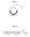
- electrodeposited copper foil produced by an electrodeposited foil production apparatus as shown in FIG. 1 is treated to prevent rust and to roughen its surface to increase bondability by a surface treatment apparatus as shown in FIG. 2.
- the electrodeposited foil production apparatus comprises a rotating drum-shaped cathode 2 (surface made of SUS or titanium) and an anode 1 (lead or precious metal oxide coated titanium electrode) arranged concentrically with respect to the cathode 2.
- a current is passed across the electrodes while circulating an electrolyte 3 to cause the copper to deposit on the surface of the cathode 2 to a predetermined thickness, then the copper is peeled off from the surface of the cathode 2 as copper foil 4.
- the copper foil at this stage is called the "untreated copper foil 4"
- the surface of the untreated copper foil 4 contacting the electrolyte 3 is called the “matt surface”
- the surface contacting the rotating drum shaped cathode 2 is called the “gloss surface”.
- the untreated copper foil 4 is improved in performance required for a printed circuit board, that is, the bondability to a resin substrate, by being passed through the surface treatment apparatus shown in FIG. 2 and subjected the continuous steps of electrochemical or chemical surface treatment, that is, roughening, metal plating, stainproofing, and silane coupling treatment. In these surface treatments, the roughening is ordinarily applied to the matt surface of the untreated copper foil.
- the resultant copper foil is used as a surface treated copper foil 8 for a printed circuit board.
- reference numerals 5 and 6 indicate the electrolyte and reference numeral 7 indicates an anode of the surface treatment apparatus.
- a PDP is a display panel using emission of light by electrodischarge and is comprised of a glass vessel evacuated and then filled with mercury gas etc. Voltage is applied to cause electrodischarge. The ultraviolet light generated at this time strikes fluorescent coating previously applied to the inside of the glass vessel to cause emission of visible light.
- PDP has mainly been used for display applications at train stations and public facilities or exhibitions and family restaurants, but recently demand for household use large-scale televisions has been increasing.
- an electromagnetic shield at the front of the display (side close to viewer).
- an electromagnetic shield for electromagnetic waves leaking from devices used in public facilities use has been made of a sheet of glass provided on its entire surface with a thin film of silver, a fine nylon mesh material plated by copper, etc.
- a type of shield comprised of a transparent film such as a polyester film on which copper foil is bonded and etched to leave a mesh of copper on the film has come into use.
- This shield is arranged in front of the display. The viewer views the light passing through parts without the mesh copper. To obtain a good image quality, the mesh has to have a good light transmission. Shields having a copper foil mesh of a width of 10 ⁇ m and a pitch of 200 ⁇ m are now being mass produced.
- the requirements on the copper foil for a PDP are similar to the requirements on copper foil for a high density printed circuit board. That is, in order to produce a copper foil mesh having a fine width, it is necessary that the roughness of the matt surface and the gloss surface of the copper foil both be small. A copper foil having a small surface roughness is required.
- electronic devices are not only being reduce in size and weight, but also are being designed for further higher frequencies along with the increase of information transfer. Up to now, a high frequency signal over 1 GHz had been used for restricted radio use such as communications for aircraft and satellite communications, but recently is being used also for familiar electronic devices such as mobile phones and wireless LAN. The printed circuit boards for such high frequencies have to use a resin superior in high frequency characteristic.
- the copper foil has to be one having less high-frequency transfer loss. That is, the higher the frequency, the more noticeable the "skin effect" where a signal passes primarily at the surface part of a conductive layer. Due to this, when using a conventional copper foil having a large unevenness, the high-frequency transfer loss is large. Therefore, it can no longer be used for such applications.
- a major factor influencing the high-frequency transfer loss is the surface roughness.
- the surface roughness of the untreated copper foil is primarily decided by the electrodeposition conditions when the copper to be deposited on the above drum-shaped cathode 2 in FIG. 1 and by the additives added to the electrolyte 3.
- General electrodeposited copper foil is roughened on its matt surface to a surface roughness of about 6 ⁇ m at a thickness of 12 ⁇ m and about 10 ⁇ m at a thicker copper foil of 70 ⁇ m in terms of the surface roughness Rz (Rz as defined in JIS B0601-1994, "Definition and Description of Surface Roughness", 5.1 “Definition of 10-Point Average Roughness”).
- Rz surface roughness as defined in JIS B0601-1994, "Definition and Description of Surface Roughness", 5.1 “Definition of 10-Point Average Roughness”
- the gloss surface (surface of side contacting drum) has gloss at first glance and seems to be smooth, but becomes a replica of the drum surface.
- the roughness is usually about 1.5 to 2.0 ⁇ m in terms of Rz in average. This is because manufacture is started in a state with the initial drum surface polished smooth, but later the drum surface is dissolved and gradually becomes rough along with continuance of manufacture of the electrodeposited copper foil due to the electrolyte being strongly acidic. If after manufacture of the electrodeposited copper foil for a certain time the drum surface becomes rough, the drum surface is polished again to smooth it, but seen on an average, the roughness is about 1.5 to 2.0 ⁇ m.
- the circuit is sometimes formed in a wave shape during etching. If becoming wavy in this way, the circuit becomes poor in linearity and the problem arises that it becomes difficult to form fine patterns. Further, in a case of using a liquid resist, while the degree is slight compared with a dry film resist, due to the difference of the dissolution rate between depressions and projections of the copper foil, the phenomenon of the shape of the circuit becoming wavy is seen in the same way. To deal with the requirement of increasing the pattern fineness, in addition to the roughness of the matt surface of the copper foil being small, it is important that the roughness of the gloss surface also be small.
- the surface of the copper foil be small in surface roughness of the side to be bonded with the film for the recognition rate and it is important that the surface roughness be small at both sides for a copper foil for use in a plasma display panel and high-frequency printed circuit board.
- the importance of surface roughness was described with reference to an electrodeposited copper foil, but a rolled copper foil also has the same problems of course.
- An object of the present invention is to provide a copper foil having a high etching factor, having superior linearity of bottom lines of a circuit pattern, having no copper partaicles remaining in the resin of the circuit pattern, capable of forming fine pattern, superior in recognition rate, and having a small high-frequency transmission loss.
- a copper foil for chip-on-film use, a plasma display panel, or a high-frequency printed circuit board obtained by rolling copper foil to smooth the surface to give a surface area of not more than 1.30 times an ideal smooth surface.
- the present invention is characterized by rolling the copper foil (below, unless otherwise alluded to, the term "copper foil” generally meaning an electrodeposited copper foil and a rolled copper foil) to smooth it to give a surface area as measured by a laser microscope (made by KEYENCE Co., model number: VK-8510) not more than 1.30 times, preferably not more than 1.20 times, of the ideal smooth surface.
- the smoothed copper foil surface is plated by at least one metal of Ni and Zn.
- the smoothed copper foil surface is plated by at least one metal of Ni and Zn.
- fine roughening particles of Cu or alloy particles of Cu and Mo or alloy particles comprising Cu and at least one element selected among a group of Ni, Co, Fe, and Cr or a mixture of the alloy particles and an oxide of at least one element selected among a group of V, Mo, and W are deposited.
- fine roughening particles are adhered to the smoothed surface uniformly and the bonding strength with a resin substrate is increased.
- the fine roughening particles deposited on the smoothed surface are further provided with at least one type of metal plating layer selected from a group of Cu, Ni, Zn, Co, V, Mo, and W.
- metal plating layer selected from a group of Cu, Ni, Zn, Co, V, Mo, and W.
- a copper foil on which fine roughening particles are deposited depending on the deposition conditions of the fine roughening particles, sometimes particles do not deposit strongly on the copper foil. Further, depending on the next step of the processing, sometimes part of the fine roughening particles peel off during the treatment and deposit on the facilities, therefore fine roughening particles resistant to falling is being sought. To meet with this requirement, it is possible to plate the surface of the fine roughening particles as explained above and thereby suppress this peeling phenomenon (falling particles).
- the outermost layer surface is treated for stainproofing.
- the outermost layer surface is treated for silane coupling.
- the outermost layer surface is treated for stainproofing and silane coupling.
- the surface of the copper foil after rolling or the surface of the fine roughening particles deposited on the surface for stainproofing or for silane coupling it is possible to prevent oxidation and discoloration of the copper foil.
- a copper foil for chip-on-film use, a plasma display panel, or a high-frequency printed circuit board obtained by rolling electrodeposited copper foil or rolled copper foil using a work roll of a predetermined surface roughness with rolling oil of a predetermined viscosity and a speed suppressed to a range where no oil pits occur, having a surface area of not more than 1.30 times an ideal smooth surface.
- the factors that decide the recognition rate in a COF are not only the transparency of a film itself, but also the surface area (surface unevenness) of the copper foil and that the recognition rate is better the closer the surface to the ideal smooth surface and the substantially permitted surface area is not more than 1.30 times the ideal smooth surface; that, second, the point of making the pattern fineness closer to the ideal in a PDP is the surface area (surface unevenness) of a copper foil and the closer the surface to the ideal smooth surface, the better the pattern fineness, but due to the balance with the bondability, it is preferable that the surface area be 1.30 to 1.1 times the ideal smooth surface; and that, third the increased speed of communication and the difference in communication speed demanded in a copper foil for a high-frequency printed circuit board relate to the surface area (surface unevenness), that the closer the copper foil surface through which the radio frequency waves pass to the ideal smooth surface, the better the communication characteristics, and that to draw out superior communication characteristics, the surface area should be not more than 1.30 times the ideal smooth surface.
- the polyimide resin with which the copper foil is bonded differs slightly in color, bonding strength with the copper foil, and other aspects of performance depending on the manufacturer.
- the polyimide film made by a certain manufacturer is slightly inferior in the recognition rate of the film itself due to its deep color, but is superior in bondability with copper foil and enables a sufficient practical bonding strength even with copper foil without roughening of the present invention.
- copper foil was rolled to decrease the surface area to not more than 1.30 times the ideal smooth surface, was chromated for stainproofing and treated for silane coupling, then was bonded with the polyimide film. The circuit was formed, then the recognition rate for confirmation of the position of the IC and the bonding strength of the two were measured. Satisfactory results were obtained in this case.
- the "ideal smooth surface” is a perfectly flat surface without any unevenness. Further, original foil of a surface area of up to 1.30 times the ideal smooth surface was plated with at least one metal of Ni or Zn and further chromated for stainproofing and treated for silane coupling. When measuring the recognition rate, bonding strength, etc., it was confirmed that satisfactory results were obtained.
- the fine roughening particles deposited on the smoothed copper foil surface may be particles of Cu, but may also be alloy particles of Cu and Mo or alloy particles comprising Cu and at least one element (I) selected among a group of Ni, Co, Fe and Cr (hereinafter described as the "particles I") or a mixture of particles I and oxides of at least one element (II) selected among a group of V, Mo, and W (hereinafter described as the "particles II").
- FR-4 or another epoxy resin used for an ordinary rigid circuit board it is possible to obtain desired bonding strength by Cu particles or alloy particles of Cu and Mo.
- the particles I for example particles of Cu-Ni alloys, Cu-Co alloys, Cu-Fe alloys, Cu-Cr alloys, etc. are preferable.
- the amount of the element (I) in the above alloy particles is preferably 0.1 to 3 mg/dm 2 foil per 1 mg/dm 2 foil of Cu, while the amount of the element (II) in the above mixture is preferably 0.02 to 0.8 mg/dm 2 foil per 1 mg/dm 2 foil of Cu.
- the reason is that in the particles I, if the amount of the element (I) is greater than 3 mg/dm 2 foil per 1 mg/dm 2 foil of Cu in the composition of the alloys, the problem arises that it is difficult to dissolve except Co when etching the circuit pattern and it remains on the resin substrate, while if the amount of the element (I) is less than 0.1 mg/dm 2 foil in the composition of the alloys, the problem arises that an increase of bonding strength with respect to a resin substrate, for example, a polyimide resin substrate inferior in the bonding strength with the copper foil cannot be expected.
- Cu-Ni alloy particles or Cu-Co alloy particles are preferable because Ni or Co itself exhibits a high bonding strength to a resin substrate like polyimide, so the alloy particles as a whole also exhibit a high bonding strength with the resin substrate.
- C-Ni alloy particles or Cu-Co alloy particles giving an amount (of deposition) of Cu to the foil of 4 to 20 mg/dm 2 in terms of absolute amount and an amount (of deposition) of Ni or Co of 0.1 to 3 mg/mgCu is particularly preferable in the sense of exhibiting an extremely high bondability.
- the particles II are comprised of a mixture of the particles I and oxide particles.
- the particles I deposit at the grain boundaries of the crystal grains, while simultaneously the element (II), for example, V, Mo, or W, forms oxide particles such as V 2 O 5 , MoO 3 , or WO 3 and deposits in a state mixed with the particles I, whereby the particles II are formed. Therefore, these particles II coexist in a suitable mutually dispersed state.
- the particles I selectively deposit on the crystal grain boundaries of the copper foil, but in that case, they tend not to uniformly deposit at all grain boundaries, but to concentrate at certain specific grain boundaries. If such a state of deposition proceeds, even if the overall amount of deposition increases, the particles I will not necessarily uniformly deposit at the grains boundaries as a whole and therefore the bonding strength with the resin substrate will fall at undeposited locations.
- the circuit forming copper foil is tin plated.
- the temperature of the Sn plating solution is very high, sometimes undercutting will occur where the plating solution penetrates between the copper foil and the film. Therefore, for such applications, it is necessary to design the composition of the fine roughening particles so as to prevent undercut.
- a composition of the fine roughening particles is preferably 0.1 to 3.0 mg/dm 2 foil of Co and 0.1 to 3.0 mg/dm 2 foil of Ni per 1 mg/dm 2 foil of Cu, more preferably 1.2 to 2.2 mg/dm 2 foil of Co and 0.1 to 2.0 mg/dm 2 foil of Ni per 1 mg/dm 2 foil of Cu, still more preferably 1.5 to 1.9 mg/dm 2 foil of Co and 1.3 to 1.7 mg/dm 2 foil of Ni per 1 mg/dm 2 foil of Cu.
- the electrodeposited copper foil or rolled copper coil used in the present invention may be any foil. It is sufficient that the rolling result in the surface area being reduced to not more than 1.30 times the ideal smooth surface. It is possible to select the necessary treatment among roughening, cover plating, Ni or Zn treatment, stainproofing, and silane coupling treatment depending on the type of the resin to be bonded to and the application.
- this copper foil is not limited to COF applications and can also be used as a copper foil for general fine pattern printed circuit boards, PDP electromagnetic shields, and high-frequency printed circuit boards.
- An untreated electrodeposited copper foil of a thickness of 10 ⁇ m, surface roughness Rz of the matt surface of 1.03 ⁇ m, and surface roughness Rz of the gloss surface of 1.20 ⁇ m was cold rolled by one pass to obtain an original foil 1 of a thickness of 9 ⁇ m.
- the rolling was performed using a smooth work roll of a surface roughness Ra (Ra as defined in JIS B0601-1994, "Definition and Description of Surface Roughness", 3.1 “Definition of Ra”) of 0.03 ⁇ m, a 4 centistoke low viscosity rolling oil, and a speed suppressed to a range where no oil pits occur.
- Ra surface roughness
- the matt surface after rolling was measured for its surface area at a 80 ⁇ m x 120 ⁇ m part (ideal smooth surface area of 9600 ⁇ m 2 ) by a laser microscope (made by KEYENCE Co., model number: VK-8510) to obtain a value of the surface area of 11,403 ⁇ m 2 . This value was 1.19 times the ideal smooth surface area. Further, the matt surface before rolling was also measured and was of 12,871 ⁇ m 2 (1.34 times).
- An untreated electrodeposited copper foil of a thickness of 15 ⁇ m was cold rolled by two passes to manufacture an original foil 2 of a thickness of 12 ⁇ m.
- the surface of this original foil 2 was measured by a laser microscope (made by KEYENCE Co., model number: VK-8510). The surface area was calculated, whereby the surface was smoothed to 1.25 times the ideal smooth surface.
- An untreated electrodeposited copper foil of a thickness of 18 ⁇ m was cold rolled by three passes to manufacture an original foil 3 of a thickness of 12 ⁇ m.
- the surface of this original foil 3 was measured by a laser microscope (made by KEYENCE Co., model number: VK-8510). The surface area was calculated, whereby the surface was smoothed to 1.22 times the ideal smooth surface.
- a rolled copper foil of a thickness of 18 ⁇ m was further cold rolled by three passes to manufacture an original foil 4 of a thickness of 12 ⁇ m.
- the surface of this original foil 4 was measured by a laser microscope (made by KEYENCE Co., model number: VK-8510). The surface area was calculated, whereby the surface was smoothed to 1.19 times the ideal surface.
- Electroplating A (nickel plating)
- Electroplating B (zinc plating)
- composition of the electroplating solution Zinc sulfate 7-hydrate 35 g/liter Sodium hydroxide 70 g/liter [Conditions] Temperature 20°C Current density 0.25 A/dm 2 Treatment time 3 seconds
- composition of the electroplating solution Copper sulfate 5-hydrate 20 g/liter Sulfuric acid 45 g/liter Arsenic (As) 140 mg/liter [Conditions] Temperature 20°C Current density 11 A/dm 2 Treatment time 3 seconds
- Electroplating G metal plating layer
- composition of the electroplating solution Cobalt sulfate 7-hydrate 76 g/liter Boric acid 30 g/liter [Conditions] Temperature 40°C pH 3.1 Current density 5.6 A/dm 2 Treatment time 5 seconds
- Electroplating H (staiproofing: cathode chromating)
- composition of the electroplating solution 3-glycidoxy propylmethoxysilane 1 g/liter [Conditions] Temperature Room temperature Treatment Dip, then squeegee, heat and dry
- the original foil 1, original foil 2, original foil 3, and original foil 4 were treated by the electroplating H for stainproofing and by the silane coupling treatment I, then bonded at a high temperature and high pressure to polyimide films. The bondability was superior.
- dry film etching resists were bonded to the surfaces of these copper foils and etched to prepare COF resin substrates. When producing the COF resin substrates, the circuits did not become wavy in shape, the circuits became extremely good in linearity, and fine patterns of a width of 15 ⁇ m and a conductor pitch of 15 ⁇ m were completed.
- the IC chips were positioned by recognition through the parts of the polyimide films from which the foils were etched, but it was also possible to easily confirm the positions of the IC chips from above and connect IC chips and COF circuits accurately. Further, the undercut phenomenon in Sn plating also could not be observed.
- the original foil 1, original foil 2, original foil 3, and original foil 4 were nickel plated by the electroplating A and zinc plated by the electroplating B, then treated for stainproofing by the electroplating H and subjected to the silane coupling treatment I.
- the copper foils were bonded at a high temperature and high pressure to polyimide films. The bondability was superior.
- dry film etching resists were bonded to the surfaces of these copper foils and etched to prepare COF resin substrates. When producing the COF resin substrates, the circuits did not become wavy in shape, the circuits became extremely good in linearity, and fine patterns of a width of 15 ⁇ m and a conductor pitch of 15 ⁇ m were completed.
- the IC chips were positioned by recognition through the parts of the polyimide films from which the foils were etched, but it was also possible to easily confirm the positions of the IC chips from above and connect IC chips and COF circuits accurately. Further, the undercut phenomenon in Sn plating also could not be observed.
- the original foil 1, original foil 2, original foil 3, and original foil 4 were finely roughened by electroplating C, then treated for stainproofing by the electroplating H and subjected to the silane coupling treatment I.
- the copper foils were coated with a polyimide resin, then heated to cure the resin to form films. The results were then aged by heating to produce copper-clad polyimide films. The bondability of the copper and polyimide films in these copper-clad polyimide films was good.
- the copper foils were bonded with dry film etching resists and etched to prepare COF resin substrates.
- the circuits did not become wavy in shape, the circuits became extremely good in linearity, and fine patterns of a width of 25 ⁇ m and a conductor pitch of 25 ⁇ m were completed.
- the IC chips were positioned by recognition through the parts of the polyimide films from which the foils were etched, but it was also possible to easily confirm the positions of the IC chips from above and connect IC chips and COF circuits accurately. Further, the undercut phenomenon in Sn plating also could not be observed.
- the original foil 1, original foil 2, original foil 3, and original foil 4 were finely roughened by electroplating D, then treated for stainproofing by the electroplating H and subjected to the silane coupling treatment I.
- the copper foils were coated with a polyimide resin, then heated to cure the resin to form films. The results were then aged by heating to produce copper-clad polyimide films. The bondability of the copper and polyimide films in these copper-clad polyimide films was good.
- the copper foils were bonded with dry film etching resists and etched to prepare COF resin substrates.
- the circuits did not become wavy in shape, the circuits became extremely good in linearity, and fine patterns of a width of 25 ⁇ m and a conductor pitch of 25 ⁇ m were completed.
- the IC chips were positioned by recognition through the parts of the polyimide films from which the foils were etched, but it was also possible to easily confirm the positions of the IC chips from above and connect IC chips and COF circuits accurately. Further, the undercut phenomenon in Sn plating also could not be observed.
- the original foil 1, original foil 2, original foil 3, and original foil 4 were finely roughened by electroplating E, then treated for stainproofing by the electroplating H and subjected to the silane coupling treatment I.
- the copper foils were coated with a polyimide resin, then heated to cure the resin to form films. The results were then aged by heating to produce copper-clad polyimide films. The bondability of the copper and polyimide films in these copper-clad polyimide films was good.
- the copper foils were bonded with dry film etching resists and etched to prepare COF resin substrates.
- the circuits did not become wavy in shape, the circuits became extremely good in linearity, and fine patterns of a width of 20 ⁇ m and a conductor pitch of 20 ⁇ m were completed.
- the IC chips were positioned by recognition through the parts of the polyimide films from which the foils were etched, but it was also possible to easily confirm the positions of the IC chips from above and connect IC chips and COF circuits accurately. Further, the undercut phenomenon in Sn plating also could not be observed.
- the original foil 1, original foil 2, original foil 3, and original foil 4 were finely roughened by electroplating F, then treated for stainproofing by the electroplating H and subjected to the silane coupling treatment I.
- the copper foils were coated with a polyimide resin, then heated to cure the resin to form films. The results were then aged by heating to produce copper-clad polyimide films. The bondability of the copper and polyimide films in these copper-clad polyimide films was good.
- the copper foils were bonded with dry film etching resists and etched to prepare COF resin substrates.
- the circuits did not become wavy in shape, the circuits became extremely good in linearity, and fine patterns of a width of 25 ⁇ m and a conductor pitch of 25 ⁇ m were completed.
- the IC chips were positioned by recognition through the parts of the polyimide films from which the foils were etched, but it was also possible to easily confirm the positions of the IC chips from above and connect IC chips and COF circuits accurately. Further, the undercut phenomenon in Sn plating also could not be observed.
- the original foil 1, the original foil 2, the original foil 3, and the original foil 4 were finely roughened by the electroplating E. With the foils in this state, sometimes the problem arises of the fine roughening particles being rubbed off by the guide roll and depositing on the surface of the roll when laminating the polyimide film during the process of production of a PDP electromagnetic shield. In order to prevent this, the fine roughening particles were plated with a covering Co metal plating layer by the electroplating G. Then, the foils were treated for stainproofing by the electroplating H and silane coupling treatment I. The copper foils were laminated to polyimide films. At the time of this process, no separation of the fine roughening particles and deposition on the guide roll were seen at all.
- PDP electromagnetic shields were coated with a liquid etching resist and etched to prepare PDP electromagnetic shields. These PDP electromagnetic shields had extremely good linearity of the circuits. PDP electromagnetic shields of fine patterns of a width of 9 ⁇ m and a conductor pitch of 200 ⁇ m were completed. These PDP electromagnetic shields satisfied the Class B requirements of EN5022 for electromagnetic shielding and can be adopted for home television sets.
- the original foil 1, the original foil 2, the original foil 3, and the original foil 4 were finely roughened by the electroplating F, then were treated for stainproofing by the electroplating H and silane coupling treatment I.
- the surface of the copper foils were covered with glass cloth prepregs impregnated with a high-frequency substrate use resin and then these were hot pressed to prepare copper-clad substrates.
- the copper foils were bonded with dry film etching resists and etched to obtain high-frequency printed circuit boards. These high-frequency printed circuit boards had extremely good linearity of the circuits.
- High-frequency printed circuit boards of patterns of a width of 100 ⁇ m and a conductor pitch of 100 ⁇ m were completed. 4 GHz signals were sent over 500 mm by these high-frequency printed circuit boards, whereupon it was found that the transmission loss was 19% less compared with a case of using ordinary copper foil and almost no time error was measured.
Landscapes
- Engineering & Computer Science (AREA)
- Chemical & Material Sciences (AREA)
- Microelectronics & Electronic Packaging (AREA)
- Materials Engineering (AREA)
- Electrochemistry (AREA)
- Metallurgy (AREA)
- Organic Chemistry (AREA)
- Manufacturing & Machinery (AREA)
- Chemical Kinetics & Catalysis (AREA)
- Electroplating Methods And Accessories (AREA)
- Parts Printed On Printed Circuit Boards (AREA)
- Manufacturing Of Printed Wiring (AREA)
- Metal Rolling (AREA)
- Conductive Materials (AREA)
- Other Surface Treatments For Metallic Materials (AREA)
- Laminated Bodies (AREA)
Applications Claiming Priority (2)
| Application Number | Priority Date | Filing Date | Title |
|---|---|---|---|
| JP2002256666 | 2002-09-02 | ||
| JP2002256666 | 2002-09-02 |
Publications (2)
| Publication Number | Publication Date |
|---|---|
| EP1394291A2 true EP1394291A2 (fr) | 2004-03-03 |
| EP1394291A3 EP1394291A3 (fr) | 2006-11-22 |
Family
ID=31492699
Family Applications (1)
| Application Number | Title | Priority Date | Filing Date |
|---|---|---|---|
| EP03019917A Withdrawn EP1394291A3 (fr) | 2002-09-02 | 2003-09-02 | Feuille de cuivre pour l'utilisation en chip-sur-film-mince, panneau d'affichage à plasma ou plaquette à circuit imprimé haute frequence |
Country Status (5)
| Country | Link |
|---|---|
| US (1) | US7172818B2 (fr) |
| EP (1) | EP1394291A3 (fr) |
| KR (1) | KR101007580B1 (fr) |
| CN (1) | CN100353819C (fr) |
| TW (1) | TW200404484A (fr) |
Cited By (2)
| Publication number | Priority date | Publication date | Assignee | Title |
|---|---|---|---|---|
| EP1562413A2 (fr) * | 2004-02-06 | 2005-08-10 | Furukawa Circuit Foil Co., Ltd. | Feuille de cuivre traitée et panneau de circuit |
| EP1452627A3 (fr) * | 2003-02-27 | 2006-02-08 | Furukawa Circuit Foil Co., Ltd. | Feuille de cuivre de blindage électromagnétique, procédé de fabrication associé et blindage électromagnétique |
Families Citing this family (20)
| Publication number | Priority date | Publication date | Assignee | Title |
|---|---|---|---|---|
| KR100559933B1 (ko) * | 2002-11-29 | 2006-03-13 | 엘에스전선 주식회사 | 저조도 동박의 전해연마방법 및 전해연마장치와 동박 |
| US20060147742A1 (en) * | 2003-02-04 | 2006-07-06 | Akira Matsuda | Composite copper foil, method of production thereof and high frequency transmission circuit using said composite copper foil |
| TW200500199A (en) * | 2003-02-12 | 2005-01-01 | Furukawa Circuit Foil | Copper foil for fine patterned printed circuits and method of production of same |
| JP4448751B2 (ja) * | 2004-09-30 | 2010-04-14 | 株式会社オーディオテクニカ | コンデンサマイクロホン |
| CN100468675C (zh) * | 2004-12-22 | 2009-03-11 | 新日铁化学株式会社 | Cof基板用层合体的制造方法 |
| TWI396779B (zh) * | 2005-02-21 | 2013-05-21 | 古河電氣工業股份有限公司 | Copper foil and its manufacturing method, and flexible printed circuit board |
| KR100649755B1 (ko) * | 2005-11-07 | 2006-11-27 | 삼성전기주식회사 | 박막 커패시터 내장된 인쇄회로기판 및 그 제조방법 |
| TW200735317A (en) * | 2006-03-14 | 2007-09-16 | Novatek Microelectronics Corp | Tape |
| US20080142249A1 (en) * | 2006-12-13 | 2008-06-19 | International Business Machines Corporation | Selective surface roughness for high speed signaling |
| KR101289803B1 (ko) * | 2008-05-16 | 2013-07-26 | 삼성테크윈 주식회사 | 회로 기판 및 그 제조 방법 |
| US9201015B2 (en) | 2011-07-14 | 2015-12-01 | International Business Machines Corporation | Plated through hole void detection in printed circuit boards by detecting a pH-sensitive component |
| CN103929874B (zh) * | 2014-04-09 | 2017-04-19 | 中国科学院微电子研究所 | 一种pcb线路板铜线路加工方法 |
| KR102274906B1 (ko) * | 2016-09-12 | 2021-07-09 | 후루카와 덴키 고교 가부시키가이샤 | 구리박 및 이것을 갖는 동장 적층판 |
| CN108930050A (zh) * | 2017-05-26 | 2018-12-04 | 湖南省正源储能材料与器件研究所 | 一种锂离子电池负极集流体用超薄电子铜箔的制备方法 |
| JP6895936B2 (ja) | 2018-09-28 | 2021-06-30 | 古河電気工業株式会社 | 表面処理銅箔、並びにこれを用いた銅張積層板及び回路基板 |
| CN110868799A (zh) * | 2019-11-15 | 2020-03-06 | 江苏上达电子有限公司 | 一种透明cof设计方法 |
| CN113737238B (zh) * | 2021-10-11 | 2023-04-11 | 中色奥博特铜铝业有限公司 | 一种超低轮廓度压延铜箔表面粗化处理方法 |
| CN114914165B (zh) * | 2022-05-06 | 2024-09-20 | 北京燕东微电子科技有限公司 | 监测晶圆腐蚀液更换周期的方法 |
| CA3221703C (fr) * | 2022-12-06 | 2026-03-10 | Sk Nexilis Co., Ltd. | Feuille de cuivre, electrode la comprenant, batterie secondaire la comprenant et methode de fabrication |
| CN116288543A (zh) * | 2023-01-16 | 2023-06-23 | 九江德福科技股份有限公司 | 一种多孔铜箔的电解生箔方法 |
Family Cites Families (37)
| Publication number | Priority date | Publication date | Assignee | Title |
|---|---|---|---|---|
| EP1132961B1 (fr) * | 1991-07-24 | 2011-01-05 | Denki Kagaku Kogyo Kabushiki Kaisha | Procédé de fabrication d'un substrat de circuit avec un élément semi-conducteur monté dessus |
| US5622782A (en) * | 1993-04-27 | 1997-04-22 | Gould Inc. | Foil with adhesion promoting layer derived from silane mixture |
| US5447619A (en) * | 1993-11-24 | 1995-09-05 | Circuit Foil Usa, Inc. | Copper foil for the manufacture of printed circuit boards and method of producing the same |
| US5482784A (en) | 1993-12-24 | 1996-01-09 | Mitsui Mining And Smelting Co., Ltd. | Printed circuit inner-layer copper foil and process for producing the same |
| JPH07314603A (ja) * | 1993-12-28 | 1995-12-05 | Nippon Denkai Kk | 銅張積層体、多層プリント回路板及びそれらの処理方法 |
| TW317575B (fr) * | 1994-01-21 | 1997-10-11 | Olin Corp | |
| TW289900B (fr) * | 1994-04-22 | 1996-11-01 | Gould Electronics Inc | |
| US6132851A (en) * | 1994-06-28 | 2000-10-17 | Ga-Tek Inc. | Adhesive compositions and copper foils and copper clad laminates using same |
| JP3709221B2 (ja) * | 1994-10-06 | 2005-10-26 | 古河サーキットフォイル株式会社 | 銅箔の表面粗化処理方法 |
| JP3313277B2 (ja) | 1995-09-22 | 2002-08-12 | 古河サーキットフォイル株式会社 | ファインパターン用電解銅箔とその製造方法 |
| JP3155920B2 (ja) * | 1996-01-16 | 2001-04-16 | 三井金属鉱業株式会社 | プリント配線板用電解銅箔及びその製造方法 |
| JPH09316643A (ja) * | 1996-02-15 | 1997-12-09 | Mitsubishi Materials Corp | 物理蒸着装置の防着部品 |
| JPH10100320A (ja) * | 1996-09-30 | 1998-04-21 | Mitsubishi Gas Chem Co Inc | 複合セラミックス板およびその製造法 |
| US5863410A (en) * | 1997-06-23 | 1999-01-26 | Circuit Foil Usa, Inc. | Process for the manufacture of high quality very low profile copper foil and copper foil produced thereby |
| KR20000011746A (ko) * | 1998-07-17 | 2000-02-25 | 미야무라 심뻬이 | 동박의건조방법및동박건조장치 |
| ES2367838T3 (es) * | 1998-09-10 | 2011-11-10 | JX Nippon Mining & Metals Corp. | Laminado que comprende una hoja de cobre tratada y procedimiento para su fabricación. |
| US6274224B1 (en) * | 1999-02-01 | 2001-08-14 | 3M Innovative Properties Company | Passive electrical article, circuit articles thereof, and circuit articles comprising a passive electrical article |
| JP2000294251A (ja) * | 1999-04-06 | 2000-10-20 | Hitachi Cable Ltd | Liイオン電池の負極集電体用銅材およびその製造方法 |
| JP2000315888A (ja) * | 1999-04-30 | 2000-11-14 | Hitachi Chem Co Ltd | 電磁波シールドフィルムの製造方法、電磁波シールドフィルム並びにこの電磁波シールドフィルムを用いた電磁波遮蔽体及びディスプレイ |
| JP3291482B2 (ja) * | 1999-08-31 | 2002-06-10 | 三井金属鉱業株式会社 | 整面電解銅箔、その製造方法および用途 |
| JP3291486B2 (ja) * | 1999-09-06 | 2002-06-10 | 三井金属鉱業株式会社 | 整面電解銅箔、その製造方法およびその用途 |
| US6270648B1 (en) * | 1999-10-22 | 2001-08-07 | Yates Foil Usa, Inc. | Process and apparatus for the manufacture of high peel-strength copper foil useful in the manufacture of printed circuit boards, and laminates made with such foil |
| JP3949871B2 (ja) * | 1999-12-10 | 2007-07-25 | 日本電解株式会社 | 粗化処理銅箔及びその製造方法 |
| US6497806B1 (en) | 2000-04-25 | 2002-12-24 | Nippon Denkai, Ltd. | Method of producing a roughening-treated copper foil |
| US6569543B2 (en) * | 2001-02-15 | 2003-05-27 | Olin Corporation | Copper foil with low profile bond enahncement |
| JP3794613B2 (ja) | 2000-05-18 | 2006-07-05 | 三井金属鉱業株式会社 | 電解銅箔の電解装置 |
| JP3622639B2 (ja) * | 2000-05-30 | 2005-02-23 | 株式会社村田製作所 | 非可逆回路素子の製造方法 |
| JP3760089B2 (ja) * | 2000-07-27 | 2006-03-29 | 日鉱金属加工株式会社 | 高周波回路用銅合金箔 |
| JP4381574B2 (ja) * | 2000-08-17 | 2009-12-09 | 日鉱金属株式会社 | 積層板用銅合金箔 |
| TW511408B (en) * | 2000-09-18 | 2002-11-21 | Nippon Denkai Kk | Method of producing copper foil for fine wiring |
| US7026059B2 (en) | 2000-09-22 | 2006-04-11 | Circuit Foil Japan Co., Ltd. | Copper foil for high-density ultrafine printed wiring boad |
| JP4429539B2 (ja) * | 2001-02-16 | 2010-03-10 | 古河電気工業株式会社 | ファインパターン用電解銅箔 |
| KR100491385B1 (ko) * | 2001-07-04 | 2005-05-24 | 닛꼬 긴조꾸 가꼬 가부시키가이샤 | 적층판용 구리합금박 |
| DE50203402D1 (de) * | 2001-07-18 | 2005-07-21 | Ferag Ag | Verfahren und Vorrichtung zum Stapeln von flachen Gegenständen |
| US6808825B2 (en) * | 2001-08-10 | 2004-10-26 | Nikko Metal Manufacturing Co., Ltd. | Copper alloy foil |
| US6847527B2 (en) * | 2001-08-24 | 2005-01-25 | 3M Innovative Properties Company | Interconnect module with reduced power distribution impedance |
| CN1301046C (zh) * | 2002-05-13 | 2007-02-14 | 三井金属鉱业株式会社 | 膜上芯片用软性印刷线路板 |
-
2003
- 2003-08-22 TW TW092123116A patent/TW200404484A/zh not_active IP Right Cessation
- 2003-08-29 US US10/651,099 patent/US7172818B2/en not_active Expired - Fee Related
- 2003-09-01 KR KR1020030060689A patent/KR101007580B1/ko not_active Expired - Fee Related
- 2003-09-02 EP EP03019917A patent/EP1394291A3/fr not_active Withdrawn
- 2003-09-02 CN CNB031593070A patent/CN100353819C/zh not_active Expired - Fee Related
Cited By (4)
| Publication number | Priority date | Publication date | Assignee | Title |
|---|---|---|---|---|
| EP1452627A3 (fr) * | 2003-02-27 | 2006-02-08 | Furukawa Circuit Foil Co., Ltd. | Feuille de cuivre de blindage électromagnétique, procédé de fabrication associé et blindage électromagnétique |
| US7476449B2 (en) | 2003-02-27 | 2009-01-13 | Furukawa Circuit Foil Co., Ltd. | Electromagnetic shielding copper foil, method of production thereof and electromagnetic shield |
| US7569282B2 (en) | 2003-02-27 | 2009-08-04 | The Furukawa Electric Co., Ltd. | Electromagnetic shielding copper foil, method of production thereof and electromagnetic shield |
| EP1562413A2 (fr) * | 2004-02-06 | 2005-08-10 | Furukawa Circuit Foil Co., Ltd. | Feuille de cuivre traitée et panneau de circuit |
Also Published As
| Publication number | Publication date |
|---|---|
| KR101007580B1 (ko) | 2011-01-14 |
| KR20040020824A (ko) | 2004-03-09 |
| TW200404484A (en) | 2004-03-16 |
| CN1491073A (zh) | 2004-04-21 |
| US7172818B2 (en) | 2007-02-06 |
| EP1394291A3 (fr) | 2006-11-22 |
| TWI347152B (fr) | 2011-08-11 |
| US20040043242A1 (en) | 2004-03-04 |
| CN100353819C (zh) | 2007-12-05 |
Similar Documents
| Publication | Publication Date | Title |
|---|---|---|
| US7172818B2 (en) | Copper foil for chip-on-film use, plasma display panel, or high-frequency printed circuit board | |
| JP2849059B2 (ja) | 印刷回路用銅箔の処理方法 | |
| KR101853519B1 (ko) | 액정 폴리머 구리 피복 적층판 및 당해 적층판에 사용하는 구리박 | |
| CN101906630B (zh) | 电解铜箔的黑色表面处理工艺 | |
| CN103266335B (zh) | 印刷电路用铜箔及覆铜箔层压板 | |
| EP2557204A1 (fr) | Feuille de cuivre pour circuit imprimé | |
| EP3000904A2 (fr) | Feuille de cuivre avec support, procédé de production associé, feuille de cuivre avec support pour carte de circuit imprimé et une telle carte | |
| JP2004238647A (ja) | 平滑化銅箔とその製造方法 | |
| JPH0529740A (ja) | プリント配線板用電解銅箔 | |
| KR101736537B1 (ko) | 고주파 회로용 동박, 고주파 회로용 구리 피복 적층판, 고주파 회로용 프린트 배선판, 고주파 회로용 캐리어가 부착된 동박, 전자 기기, 및 프린트 배선판의 제조 방법 | |
| JP2013155415A (ja) | 高周波伝送用表面処理銅箔、高周波伝送用積層板及び高周波伝送用プリント配線板 | |
| JP2004119961A (ja) | チップオンフィルム用、プラズマディスプレイ用、または高周波プリント配線板用銅箔 | |
| EP2312022A1 (fr) | Feuille en cuivre traitée en surface et stratifié à gaine en cuivre | |
| US6939622B2 (en) | Chip-on-film use copper foil | |
| JP4202840B2 (ja) | 銅箔及びその製造方法 | |
| JP2005206915A (ja) | プリント配線板用銅箔及びその製造方法 | |
| JP4429539B2 (ja) | ファインパターン用電解銅箔 | |
| EP0758840B1 (fr) | Feuille de cuivre pour circuit imprime multicouche a haute densite | |
| US7215235B2 (en) | Conductive substrate with resistance layer, resistance board, and resistance circuit board | |
| CN111194362B (zh) | 表面处理铜箔、以及使用其的覆铜板及印刷配线板 | |
| JP2631061B2 (ja) | プリント回路用銅箔及びその製造方法 | |
| US5304428A (en) | Copper foil for printed circuit boards | |
| JP5373993B1 (ja) | キャリア付き銅箔 |
Legal Events
| Date | Code | Title | Description |
|---|---|---|---|
| PUAI | Public reference made under article 153(3) epc to a published international application that has entered the european phase |
Free format text: ORIGINAL CODE: 0009012 |
|
| AK | Designated contracting states |
Kind code of ref document: A2 Designated state(s): AT BE BG CH CY CZ DE DK EE ES FI FR GB GR HU IE IT LI LU MC NL PT RO SE SI SK TR |
|
| AX | Request for extension of the european patent |
Extension state: AL LT LV MK |
|
| PUAL | Search report despatched |
Free format text: ORIGINAL CODE: 0009013 |
|
| AK | Designated contracting states |
Kind code of ref document: A3 Designated state(s): AT BE BG CH CY CZ DE DK EE ES FI FR GB GR HU IE IT LI LU MC NL PT RO SE SI SK TR |
|
| AX | Request for extension of the european patent |
Extension state: AL LT LV MK |
|
| 17P | Request for examination filed |
Effective date: 20070301 |
|
| AKX | Designation fees paid |
Designated state(s): DE FR LU |
|
| 17Q | First examination report despatched |
Effective date: 20071113 |
|
| RAP1 | Party data changed (applicant data changed or rights of an application transferred) |
Owner name: THE FURUKAWA ELECTRIC CO., LTD. |
|
| STAA | Information on the status of an ep patent application or granted ep patent |
Free format text: STATUS: THE APPLICATION IS DEEMED TO BE WITHDRAWN |
|
| 18D | Application deemed to be withdrawn |
Effective date: 20150331 |