EP1380425B1 - Method of producing microstructure, and method of producing liquid discharge head - Google Patents
Method of producing microstructure, and method of producing liquid discharge head Download PDFInfo
- Publication number
- EP1380425B1 EP1380425B1 EP03015760A EP03015760A EP1380425B1 EP 1380425 B1 EP1380425 B1 EP 1380425B1 EP 03015760 A EP03015760 A EP 03015760A EP 03015760 A EP03015760 A EP 03015760A EP 1380425 B1 EP1380425 B1 EP 1380425B1
- Authority
- EP
- European Patent Office
- Prior art keywords
- flow path
- layer
- liquid flow
- pattern
- photosensitive material
- Prior art date
- Legal status (The legal status is an assumption and is not a legal conclusion. Google has not performed a legal analysis and makes no representation as to the accuracy of the status listed.)
- Expired - Lifetime
Links
- 239000007788 liquid Substances 0.000 title claims description 186
- 238000000034 method Methods 0.000 title claims description 132
- 239000010410 layer Substances 0.000 claims description 140
- 239000000463 material Substances 0.000 claims description 93
- 239000000758 substrate Substances 0.000 claims description 76
- 230000008569 process Effects 0.000 claims description 38
- 239000011347 resin Substances 0.000 claims description 26
- 229920005989 resin Polymers 0.000 claims description 26
- 238000011161 development Methods 0.000 claims description 24
- 230000005865 ionizing radiation Effects 0.000 claims description 22
- 229920001577 copolymer Polymers 0.000 claims description 20
- -1 azo compound Chemical class 0.000 claims description 19
- VVQNEPGJFQJSBK-UHFFFAOYSA-N Methyl methacrylate Chemical compound COC(=O)C(C)=C VVQNEPGJFQJSBK-UHFFFAOYSA-N 0.000 claims description 15
- CERQOIWHTDAKMF-UHFFFAOYSA-N Methacrylic acid Chemical compound CC(=C)C(O)=O CERQOIWHTDAKMF-UHFFFAOYSA-N 0.000 claims description 13
- 229920006027 ternary co-polymer Polymers 0.000 claims description 11
- CERQOIWHTDAKMF-UHFFFAOYSA-M Methacrylate Chemical compound CC(=C)C([O-])=O CERQOIWHTDAKMF-UHFFFAOYSA-M 0.000 claims description 10
- 238000000059 patterning Methods 0.000 claims description 10
- XLYOFNOQVPJJNP-UHFFFAOYSA-N water Substances O XLYOFNOQVPJJNP-UHFFFAOYSA-N 0.000 claims description 9
- HZAXFHJVJLSVMW-UHFFFAOYSA-N 2-Aminoethan-1-ol Chemical compound NCCO HZAXFHJVJLSVMW-UHFFFAOYSA-N 0.000 claims description 8
- YNAVUWVOSKDBBP-UHFFFAOYSA-N Morpholine Chemical compound C1COCCN1 YNAVUWVOSKDBBP-UHFFFAOYSA-N 0.000 claims description 7
- 230000002165 photosensitisation Effects 0.000 claims description 7
- 239000003504 photosensitizing agent Substances 0.000 claims description 7
- 125000004432 carbon atom Chemical group C* 0.000 claims description 6
- 230000001678 irradiating effect Effects 0.000 claims description 6
- 150000002576 ketones Chemical class 0.000 claims description 6
- 238000004132 cross linking Methods 0.000 claims description 5
- 239000003505 polymerization initiator Substances 0.000 claims description 5
- 125000000217 alkyl group Chemical group 0.000 claims description 4
- 239000011247 coating layer Substances 0.000 claims description 4
- 125000004435 hydrogen atom Chemical group [H]* 0.000 claims description 4
- QJGQUHMNIGDVPM-UHFFFAOYSA-N nitrogen group Chemical group [N] QJGQUHMNIGDVPM-UHFFFAOYSA-N 0.000 claims description 4
- 239000003960 organic solvent Substances 0.000 claims description 4
- 150000002978 peroxides Chemical class 0.000 claims description 4
- 238000010526 radical polymerization reaction Methods 0.000 claims description 4
- 150000001875 compounds Chemical class 0.000 claims description 3
- 125000004122 cyclic group Chemical group 0.000 claims description 3
- 229940028356 diethylene glycol monobutyl ether Drugs 0.000 claims description 3
- 239000000428 dust Substances 0.000 claims description 3
- 238000010438 heat treatment Methods 0.000 claims description 3
- JCGNDDUYTRNOFT-UHFFFAOYSA-N oxolane-2,4-dione Chemical compound O=C1COC(=O)C1 JCGNDDUYTRNOFT-UHFFFAOYSA-N 0.000 claims description 3
- POAOYUHQDCAZBD-UHFFFAOYSA-N 2-butoxyethanol Chemical compound CCCCOCCO POAOYUHQDCAZBD-UHFFFAOYSA-N 0.000 claims description 2
- 238000006482 condensation reaction Methods 0.000 claims description 2
- 230000018044 dehydration Effects 0.000 claims description 2
- 238000006297 dehydration reaction Methods 0.000 claims description 2
- 239000004925 Acrylic resin Substances 0.000 claims 2
- 229920000178 Acrylic resin Polymers 0.000 claims 2
- MTHSVFCYNBDYFN-UHFFFAOYSA-N diethylene glycol Chemical compound OCCOCCO MTHSVFCYNBDYFN-UHFFFAOYSA-N 0.000 claims 2
- 238000004519 manufacturing process Methods 0.000 description 46
- 239000000243 solution Substances 0.000 description 34
- 238000000576 coating method Methods 0.000 description 30
- 239000011248 coating agent Substances 0.000 description 23
- 230000018109 developmental process Effects 0.000 description 22
- 239000010408 film Substances 0.000 description 22
- 230000035945 sensitivity Effects 0.000 description 12
- 239000002904 solvent Substances 0.000 description 12
- XUIMIQQOPSSXEZ-UHFFFAOYSA-N Silicon Chemical compound [Si] XUIMIQQOPSSXEZ-UHFFFAOYSA-N 0.000 description 11
- 238000007599 discharging Methods 0.000 description 11
- 229910052710 silicon Inorganic materials 0.000 description 11
- 239000010703 silicon Substances 0.000 description 11
- 239000003513 alkali Substances 0.000 description 10
- 229920002120 photoresistant polymer Polymers 0.000 description 9
- NTIZESTWPVYFNL-UHFFFAOYSA-N Methyl isobutyl ketone Chemical compound CC(C)CC(C)=O NTIZESTWPVYFNL-UHFFFAOYSA-N 0.000 description 8
- UIHCLUNTQKBZGK-UHFFFAOYSA-N Methyl isobutyl ketone Natural products CCC(C)C(C)=O UIHCLUNTQKBZGK-UHFFFAOYSA-N 0.000 description 8
- 230000015572 biosynthetic process Effects 0.000 description 8
- 229940043265 methyl isobutyl ketone Drugs 0.000 description 8
- 239000000203 mixture Substances 0.000 description 8
- 239000005871 repellent Substances 0.000 description 8
- 239000004065 semiconductor Substances 0.000 description 8
- 238000004528 spin coating Methods 0.000 description 8
- 238000010521 absorption reaction Methods 0.000 description 7
- 239000006185 dispersion Substances 0.000 description 7
- 238000005530 etching Methods 0.000 description 7
- KFZMGEQAYNKOFK-UHFFFAOYSA-N Isopropanol Chemical compound CC(C)O KFZMGEQAYNKOFK-UHFFFAOYSA-N 0.000 description 6
- 238000006243 chemical reaction Methods 0.000 description 6
- 230000000694 effects Effects 0.000 description 6
- 238000012545 processing Methods 0.000 description 6
- WGTYBPLFGIVFAS-UHFFFAOYSA-M tetramethylammonium hydroxide Chemical compound [OH-].C[N+](C)(C)C WGTYBPLFGIVFAS-UHFFFAOYSA-M 0.000 description 6
- CTQNGGLPUBDAKN-UHFFFAOYSA-N O-Xylene Chemical compound CC1=CC=CC=C1C CTQNGGLPUBDAKN-UHFFFAOYSA-N 0.000 description 5
- 238000000862 absorption spectrum Methods 0.000 description 5
- 230000008859 change Effects 0.000 description 5
- 239000003795 chemical substances by application Substances 0.000 description 5
- 239000000178 monomer Substances 0.000 description 5
- 229920003229 poly(methyl methacrylate) Polymers 0.000 description 5
- 229920000642 polymer Polymers 0.000 description 5
- 239000004926 polymethyl methacrylate Substances 0.000 description 5
- 239000008096 xylene Substances 0.000 description 5
- RRHGJUQNOFWUDK-UHFFFAOYSA-N Isoprene Chemical compound CC(=C)C=C RRHGJUQNOFWUDK-UHFFFAOYSA-N 0.000 description 4
- 238000010276 construction Methods 0.000 description 4
- 238000007796 conventional method Methods 0.000 description 4
- 238000005520 cutting process Methods 0.000 description 4
- JHIVVAPYMSGYDF-UHFFFAOYSA-N cyclohexanone Chemical compound O=C1CCCCC1 JHIVVAPYMSGYDF-UHFFFAOYSA-N 0.000 description 4
- 238000000354 decomposition reaction Methods 0.000 description 4
- 238000011156 evaluation Methods 0.000 description 4
- 238000000206 photolithography Methods 0.000 description 4
- 239000011342 resin composition Substances 0.000 description 4
- 239000000126 substance Substances 0.000 description 4
- GYCMBHHDWRMZGG-UHFFFAOYSA-N Methylacrylonitrile Chemical compound CC(=C)C#N GYCMBHHDWRMZGG-UHFFFAOYSA-N 0.000 description 3
- 239000004793 Polystyrene Substances 0.000 description 3
- 150000007942 carboxylates Chemical class 0.000 description 3
- 239000012528 membrane Substances 0.000 description 3
- 230000003287 optical effect Effects 0.000 description 3
- 229920002223 polystyrene Polymers 0.000 description 3
- 230000002940 repellent Effects 0.000 description 3
- VZCYOOQTPOCHFL-OWOJBTEDSA-N Fumaric acid Chemical compound OC(=O)\C=C\C(O)=O VZCYOOQTPOCHFL-OWOJBTEDSA-N 0.000 description 2
- 229920001665 Poly-4-vinylphenol Polymers 0.000 description 2
- 229920002614 Polyether block amide Polymers 0.000 description 2
- 229910052581 Si3N4 Inorganic materials 0.000 description 2
- 150000008065 acid anhydrides Chemical class 0.000 description 2
- QVGXLLKOCUKJST-UHFFFAOYSA-N atomic oxygen Chemical compound [O] QVGXLLKOCUKJST-UHFFFAOYSA-N 0.000 description 2
- 239000002131 composite material Substances 0.000 description 2
- 230000000593 degrading effect Effects 0.000 description 2
- 238000013461 design Methods 0.000 description 2
- 238000004090 dissolution Methods 0.000 description 2
- 238000001312 dry etching Methods 0.000 description 2
- LYCAIKOWRPUZTN-UHFFFAOYSA-N ethylene glycol Natural products OCCO LYCAIKOWRPUZTN-UHFFFAOYSA-N 0.000 description 2
- VOZRXNHHFUQHIL-UHFFFAOYSA-N glycidyl methacrylate Chemical compound CC(=C)C(=O)OCC1CO1 VOZRXNHHFUQHIL-UHFFFAOYSA-N 0.000 description 2
- WGCNASOHLSPBMP-UHFFFAOYSA-N hydroxyacetaldehyde Natural products OCC=O WGCNASOHLSPBMP-UHFFFAOYSA-N 0.000 description 2
- 238000003475 lamination Methods 0.000 description 2
- 239000002346 layers by function Substances 0.000 description 2
- FPYJFEHAWHCUMM-UHFFFAOYSA-N maleic anhydride Chemical compound O=C1OC(=O)C=C1 FPYJFEHAWHCUMM-UHFFFAOYSA-N 0.000 description 2
- LPEKGGXMPWTOCB-UHFFFAOYSA-N methyl 2-hydroxypropionate Chemical group COC(=O)C(C)O LPEKGGXMPWTOCB-UHFFFAOYSA-N 0.000 description 2
- QVEIBLDXZNGPHR-UHFFFAOYSA-N naphthalene-1,4-dione;diazide Chemical class [N-]=[N+]=[N-].[N-]=[N+]=[N-].C1=CC=C2C(=O)C=CC(=O)C2=C1 QVEIBLDXZNGPHR-UHFFFAOYSA-N 0.000 description 2
- 229920003986 novolac Polymers 0.000 description 2
- 239000001301 oxygen Substances 0.000 description 2
- 229910052760 oxygen Inorganic materials 0.000 description 2
- 238000001782 photodegradation Methods 0.000 description 2
- 239000011241 protective layer Substances 0.000 description 2
- 230000007261 regionalization Effects 0.000 description 2
- HQVNEWCFYHHQES-UHFFFAOYSA-N silicon nitride Chemical compound N12[Si]34N5[Si]62N3[Si]51N64 HQVNEWCFYHHQES-UHFFFAOYSA-N 0.000 description 2
- 239000007787 solid Substances 0.000 description 2
- 238000007669 thermal treatment Methods 0.000 description 2
- YTJDSANDEZLYOU-UHFFFAOYSA-N 1,1,1,3,3,3-hexafluoro-2-[4-(1,1,1,3,3,3-hexafluoro-2-hydroxypropan-2-yl)phenyl]propan-2-ol Chemical compound FC(F)(F)C(C(F)(F)F)(O)C1=CC=C(C(O)(C(F)(F)F)C(F)(F)F)C=C1 YTJDSANDEZLYOU-UHFFFAOYSA-N 0.000 description 1
- WQMWHMMJVJNCAL-UHFFFAOYSA-N 2,4-dimethylpenta-1,4-dien-3-one Chemical compound CC(=C)C(=O)C(C)=C WQMWHMMJVJNCAL-UHFFFAOYSA-N 0.000 description 1
- IEMNEAVSEGLTHB-UHFFFAOYSA-N 2-[[4-[1,1,1,3,3,3-hexafluoro-2-[4-(oxiran-2-ylmethoxy)phenyl]propan-2-yl]phenoxy]methyl]oxirane Chemical compound C=1C=C(OCC2OC2)C=CC=1C(C(F)(F)F)(C(F)(F)F)C(C=C1)=CC=C1OCC1CO1 IEMNEAVSEGLTHB-UHFFFAOYSA-N 0.000 description 1
- OECTYKWYRCHAKR-UHFFFAOYSA-N 4-vinylcyclohexene dioxide Chemical compound C1OC1C1CC2OC2CC1 OECTYKWYRCHAKR-UHFFFAOYSA-N 0.000 description 1
- 229910003862 HfB2 Inorganic materials 0.000 description 1
- 239000004642 Polyimide Substances 0.000 description 1
- 239000006087 Silane Coupling Agent Substances 0.000 description 1
- 238000001015 X-ray lithography Methods 0.000 description 1
- 239000002253 acid Substances 0.000 description 1
- 239000012790 adhesive layer Substances 0.000 description 1
- 230000004075 alteration Effects 0.000 description 1
- 239000007864 aqueous solution Substances 0.000 description 1
- 239000003849 aromatic solvent Substances 0.000 description 1
- 230000008901 benefit Effects 0.000 description 1
- 150000001732 carboxylic acid derivatives Chemical class 0.000 description 1
- 150000001768 cations Chemical class 0.000 description 1
- 239000000919 ceramic Substances 0.000 description 1
- 238000003776 cleavage reaction Methods 0.000 description 1
- 230000003247 decreasing effect Effects 0.000 description 1
- XXJWXESWEXIICW-UHFFFAOYSA-N diethylene glycol monoethyl ether Chemical compound CCOCCOCCO XXJWXESWEXIICW-UHFFFAOYSA-N 0.000 description 1
- 229940075557 diethylene glycol monoethyl ether Drugs 0.000 description 1
- SBZXBUIDTXKZTM-UHFFFAOYSA-N diglyme Chemical compound COCCOCCOC SBZXBUIDTXKZTM-UHFFFAOYSA-N 0.000 description 1
- 238000009826 distribution Methods 0.000 description 1
- 238000005323 electroforming Methods 0.000 description 1
- 238000010894 electron beam technology Methods 0.000 description 1
- 239000003822 epoxy resin Substances 0.000 description 1
- 230000005281 excited state Effects 0.000 description 1
- 238000009501 film coating Methods 0.000 description 1
- 239000001530 fumaric acid Substances 0.000 description 1
- 239000011521 glass Substances 0.000 description 1
- 230000009477 glass transition Effects 0.000 description 1
- 230000006872 improvement Effects 0.000 description 1
- 238000005342 ion exchange Methods 0.000 description 1
- 150000002500 ions Chemical group 0.000 description 1
- 230000005499 meniscus Effects 0.000 description 1
- QSHDDOUJBYECFT-UHFFFAOYSA-N mercury Chemical compound [Hg] QSHDDOUJBYECFT-UHFFFAOYSA-N 0.000 description 1
- 229910052753 mercury Inorganic materials 0.000 description 1
- 239000002184 metal Substances 0.000 description 1
- 229910052751 metal Inorganic materials 0.000 description 1
- IWVKTOUOPHGZRX-UHFFFAOYSA-N methyl 2-methylprop-2-enoate;2-methylprop-2-enoic acid Chemical compound CC(=C)C(O)=O.COC(=O)C(C)=C IWVKTOUOPHGZRX-UHFFFAOYSA-N 0.000 description 1
- 238000002156 mixing Methods 0.000 description 1
- 239000012299 nitrogen atmosphere Substances 0.000 description 1
- 238000005457 optimization Methods 0.000 description 1
- 239000002245 particle Substances 0.000 description 1
- 239000012466 permeate Substances 0.000 description 1
- 239000004033 plastic Substances 0.000 description 1
- 229920003023 plastic Polymers 0.000 description 1
- 229920000647 polyepoxide Polymers 0.000 description 1
- 229920001721 polyimide Polymers 0.000 description 1
- 230000000379 polymerizing effect Effects 0.000 description 1
- 229920006215 polyvinyl ketone Polymers 0.000 description 1
- 239000000843 powder Substances 0.000 description 1
- 150000003254 radicals Chemical class 0.000 description 1
- 238000000985 reflectance spectrum Methods 0.000 description 1
- 150000003839 salts Chemical class 0.000 description 1
- 238000005488 sandblasting Methods 0.000 description 1
- 230000007017 scission Effects 0.000 description 1
- 238000003892 spreading Methods 0.000 description 1
- 230000007480 spreading Effects 0.000 description 1
- 230000006641 stabilisation Effects 0.000 description 1
- 238000011105 stabilization Methods 0.000 description 1
- 238000012360 testing method Methods 0.000 description 1
- 230000008719 thickening Effects 0.000 description 1
- 239000010409 thin film Substances 0.000 description 1
- VZCYOOQTPOCHFL-UHFFFAOYSA-N trans-butenedioic acid Natural products OC(=O)C=CC(O)=O VZCYOOQTPOCHFL-UHFFFAOYSA-N 0.000 description 1
Images


Classifications
-
- B—PERFORMING OPERATIONS; TRANSPORTING
- B41—PRINTING; LINING MACHINES; TYPEWRITERS; STAMPS
- B41J—TYPEWRITERS; SELECTIVE PRINTING MECHANISMS, i.e. MECHANISMS PRINTING OTHERWISE THAN FROM A FORME; CORRECTION OF TYPOGRAPHICAL ERRORS
- B41J2/00—Typewriters or selective printing mechanisms characterised by the printing or marking process for which they are designed
- B41J2/005—Typewriters or selective printing mechanisms characterised by the printing or marking process for which they are designed characterised by bringing liquid or particles selectively into contact with a printing material
- B41J2/01—Ink jet
- B41J2/135—Nozzles
- B41J2/16—Production of nozzles
- B41J2/1621—Manufacturing processes
- B41J2/1626—Manufacturing processes etching
- B41J2/1628—Manufacturing processes etching dry etching
-
- B—PERFORMING OPERATIONS; TRANSPORTING
- B41—PRINTING; LINING MACHINES; TYPEWRITERS; STAMPS
- B41J—TYPEWRITERS; SELECTIVE PRINTING MECHANISMS, i.e. MECHANISMS PRINTING OTHERWISE THAN FROM A FORME; CORRECTION OF TYPOGRAPHICAL ERRORS
- B41J2/00—Typewriters or selective printing mechanisms characterised by the printing or marking process for which they are designed
- B41J2/005—Typewriters or selective printing mechanisms characterised by the printing or marking process for which they are designed characterised by bringing liquid or particles selectively into contact with a printing material
- B41J2/01—Ink jet
- B41J2/135—Nozzles
- B41J2/14—Structure thereof only for on-demand ink jet heads
- B41J2/14016—Structure of bubble jet print heads
- B41J2/14032—Structure of the pressure chamber
- B41J2/1404—Geometrical characteristics
-
- B—PERFORMING OPERATIONS; TRANSPORTING
- B41—PRINTING; LINING MACHINES; TYPEWRITERS; STAMPS
- B41J—TYPEWRITERS; SELECTIVE PRINTING MECHANISMS, i.e. MECHANISMS PRINTING OTHERWISE THAN FROM A FORME; CORRECTION OF TYPOGRAPHICAL ERRORS
- B41J2/00—Typewriters or selective printing mechanisms characterised by the printing or marking process for which they are designed
- B41J2/005—Typewriters or selective printing mechanisms characterised by the printing or marking process for which they are designed characterised by bringing liquid or particles selectively into contact with a printing material
- B41J2/01—Ink jet
- B41J2/135—Nozzles
- B41J2/16—Production of nozzles
- B41J2/1601—Production of bubble jet print heads
- B41J2/1603—Production of bubble jet print heads of the front shooter type
-
- B—PERFORMING OPERATIONS; TRANSPORTING
- B41—PRINTING; LINING MACHINES; TYPEWRITERS; STAMPS
- B41J—TYPEWRITERS; SELECTIVE PRINTING MECHANISMS, i.e. MECHANISMS PRINTING OTHERWISE THAN FROM A FORME; CORRECTION OF TYPOGRAPHICAL ERRORS
- B41J2/00—Typewriters or selective printing mechanisms characterised by the printing or marking process for which they are designed
- B41J2/005—Typewriters or selective printing mechanisms characterised by the printing or marking process for which they are designed characterised by bringing liquid or particles selectively into contact with a printing material
- B41J2/01—Ink jet
- B41J2/135—Nozzles
- B41J2/16—Production of nozzles
- B41J2/1621—Manufacturing processes
- B41J2/1626—Manufacturing processes etching
- B41J2/1629—Manufacturing processes etching wet etching
-
- B—PERFORMING OPERATIONS; TRANSPORTING
- B41—PRINTING; LINING MACHINES; TYPEWRITERS; STAMPS
- B41J—TYPEWRITERS; SELECTIVE PRINTING MECHANISMS, i.e. MECHANISMS PRINTING OTHERWISE THAN FROM A FORME; CORRECTION OF TYPOGRAPHICAL ERRORS
- B41J2/00—Typewriters or selective printing mechanisms characterised by the printing or marking process for which they are designed
- B41J2/005—Typewriters or selective printing mechanisms characterised by the printing or marking process for which they are designed characterised by bringing liquid or particles selectively into contact with a printing material
- B41J2/01—Ink jet
- B41J2/135—Nozzles
- B41J2/16—Production of nozzles
- B41J2/1621—Manufacturing processes
- B41J2/1631—Manufacturing processes photolithography
-
- B—PERFORMING OPERATIONS; TRANSPORTING
- B41—PRINTING; LINING MACHINES; TYPEWRITERS; STAMPS
- B41J—TYPEWRITERS; SELECTIVE PRINTING MECHANISMS, i.e. MECHANISMS PRINTING OTHERWISE THAN FROM A FORME; CORRECTION OF TYPOGRAPHICAL ERRORS
- B41J2/00—Typewriters or selective printing mechanisms characterised by the printing or marking process for which they are designed
- B41J2/005—Typewriters or selective printing mechanisms characterised by the printing or marking process for which they are designed characterised by bringing liquid or particles selectively into contact with a printing material
- B41J2/01—Ink jet
- B41J2/135—Nozzles
- B41J2/16—Production of nozzles
- B41J2/1621—Manufacturing processes
- B41J2/1637—Manufacturing processes molding
- B41J2/1639—Manufacturing processes molding sacrificial molding
-
- B—PERFORMING OPERATIONS; TRANSPORTING
- B41—PRINTING; LINING MACHINES; TYPEWRITERS; STAMPS
- B41J—TYPEWRITERS; SELECTIVE PRINTING MECHANISMS, i.e. MECHANISMS PRINTING OTHERWISE THAN FROM A FORME; CORRECTION OF TYPOGRAPHICAL ERRORS
- B41J2/00—Typewriters or selective printing mechanisms characterised by the printing or marking process for which they are designed
- B41J2/005—Typewriters or selective printing mechanisms characterised by the printing or marking process for which they are designed characterised by bringing liquid or particles selectively into contact with a printing material
- B41J2/01—Ink jet
- B41J2/135—Nozzles
- B41J2/16—Production of nozzles
- B41J2/1621—Manufacturing processes
- B41J2/164—Manufacturing processes thin film formation
- B41J2/1645—Manufacturing processes thin film formation thin film formation by spincoating
-
- B—PERFORMING OPERATIONS; TRANSPORTING
- B41—PRINTING; LINING MACHINES; TYPEWRITERS; STAMPS
- B41J—TYPEWRITERS; SELECTIVE PRINTING MECHANISMS, i.e. MECHANISMS PRINTING OTHERWISE THAN FROM A FORME; CORRECTION OF TYPOGRAPHICAL ERRORS
- B41J2202/00—Embodiments of or processes related to ink-jet or thermal heads
- B41J2202/01—Embodiments of or processes related to ink-jet heads
- B41J2202/11—Embodiments of or processes related to ink-jet heads characterised by specific geometrical characteristics
-
- Y—GENERAL TAGGING OF NEW TECHNOLOGICAL DEVELOPMENTS; GENERAL TAGGING OF CROSS-SECTIONAL TECHNOLOGIES SPANNING OVER SEVERAL SECTIONS OF THE IPC; TECHNICAL SUBJECTS COVERED BY FORMER USPC CROSS-REFERENCE ART COLLECTIONS [XRACs] AND DIGESTS
- Y10—TECHNICAL SUBJECTS COVERED BY FORMER USPC
- Y10T—TECHNICAL SUBJECTS COVERED BY FORMER US CLASSIFICATION
- Y10T29/00—Metal working
- Y10T29/49—Method of mechanical manufacture
- Y10T29/49401—Fluid pattern dispersing device making, e.g., ink jet
Definitions
- the present invention relates to a method of producing a micro structure suitable for the production of a liquid jet recording head (which may be referred to as a liquid discharge head) for generating small droplets of a recording solution used in an ink jet recording method, a method of producing a liquid jet recording head using this method and a liquid jet recording head obtained thereby.
- the present invention relates to a technique useful for a method for producing a liquid flow path shape for achieving a high speed recording process and a head thereof.
- the present invention allows to produce an ink jet head with high precision.
- a liquid discharge head which is adapted to an ink jet recording method (liquid discharge recording method) for performing recording by discharging a recording liquid such as ink, generally includes a liquid flow path, a liquid discharge energy generating unit formed on parts of the liquid flow path and a fine recording liquid discharge port (hereinafter, referred to as "orifice") for discharging the liquid of the liquid flow path by a heat energy of the liquid discharge energy generating unit.
- methods for producing such a liquid discharge recording head include, for example, (1) a method in which a through hole for supplying ink is formed on an element substrate with heaters for generating a heat energy to discharge a liquid, a drive circuit for driving these heaters and so on, the wall of the liquid flow path is patterned by negative photosensitive resist and a plate with an ink discharge port is bonded thereto by electroforming or excimer laser working; and (2) a method in which an element substrate formed in the same way as the above method is prepared, a liquid flow path and an ink discharge port are formed on a resin film (preferably, polyimide) coated with an adhesive layer by excimer laser and then a processed plate of a liquid flow path structure and the element substrate are bonded by applying a heat and a pressure.
- a resin film preferably, polyimide
- the distance between the heaters and the discharge port affecting a discharge amount must be as short as possible in order to enable the discharge of a small droplet of liquid for high quality recording.
- Japanese Patent Application Laid-Open No. 6-45242 discloses an ink jet head production method (hereinafter, abbreviated as "patterning method") in which the pattern of a liquid flow path is formed of a photosensitive material on a substrate with a liquid discharge energy generating element, a coating resin layer is coated on the substrate for coating the pattern, an ink discharge port communicating with the pattern of the liquid flow path is formed on the coating resin layer and then the photosensitive material used in the pattern is removed.
- the photosensitive material is a positive resist from a viewpoint of removal convenience.
- Japanese Patent Application Laid-Open No. 10-291317 discloses an implementation of a change of the shape of a liquid flow path in a three-dimensional direction, that is, in an interplanar direction in parallel with the element substrate and in a height direction from an element substrate, by controlling a processing depth of a resin film by partially changing the opacity of a laser mask in the excimer laser working of the liquid flow path.
- the excimer laser used in this working is different from the one used in exposure of a semiconductor but is a laser of a high brightness used in a broad band and suppresses a deviation of illuminance within a laser irradiation surface, thereby making it difficult to implement the stabilization of a laser illuminance.
- the unevenness of the discharge characteristics caused by a deviation of a processed shape between discharge nozzles is recognized as a spot in an image, thus it is a big task to achieve the improvement of a processing precision.
- Japanese Patent Application Laid-Open No. 4-216952 discloses a method in which a first layer of negative resist is formed on a substrate, a latent image of a desired pattern is formed, the first layer is coated by a second layer of negative resist, a latent image of a desired pattern is formed only no the second layer, and finally the latent image of the pattern of the upper and lower layers are developed.
- the negative resists of the two upper and lower layers have a different sensitive wavelength region from each other.
- the both upper and lower resist layers are ones sensitive to ultra violet (UV) rays, or the negative upper resist layer is one sensitive to ultra violet rays and the negative lower resist layer is one sensitive to ionizing radiation such as deep-UV, electron beams, X-rays and so on.
- UV ultra violet
- the negative resist layer is one sensitive to ultra violet rays
- the negative lower resist layer is one sensitive to ionizing radiation such as deep-UV, electron beams, X-rays and so on.
- the present inventors studied the application of the technique disclosed in Japanese Patent Application Laid-Open No. 4-216952 to the above-mentioned pattern forming method and thought that, if the technique of Japanese Patent Application Laid-Open No. 4-216952 is applied to the formation of the pattern of the liquid flow path in the pattern forming method, the height of a positive resist which forms the pattern of the liquid flow path can be changed locally.
- an alkali development positive photoresist comprising a composite of alkali soluble resin (Novolak resin or polyvinylphenol) and naphthoquinone diazide derivative as the resist which is soluble, removable and sensitive to UV; polymethylisopropenyl ketone (PMIPK) as the resist sensitive to ionizing radiation; further, to form upper and lower layers having a different pattern with respect to the substrate, as disclosed in Japanese Patent Application Laid-Open No. 4-216952 .
- this alkali development positive photoresist could not be adapted to the pattern formation of two layers since it is instantly dissolved in a developing solution of PMIPK.
- this invention is focused on finding a combination of positive photosensitive materials of upper and lower layers capable of forming a pattern that is changed in shape in a height direction with respect to the substrate in the pattern forming method.
- EP-A-1 275 508 discloses a method for manufacturing a microstructure, a method for manufacturing a liquid discharge head and a liquid discharge head.
- EP-A-0 734 866 discloses a method for manufacturing a liquid discharge head and a liquid discharge head.
- EP-A-0 867 292 discloses a nozzle plate for an ink jet print head liquid discharge head and a method for manufacturing the same.
- the present invention is designed in consideration of the problems of the prior art, and therefore it is an object of the present invention to provide a method of producing a micro structure useful for producing a liquid discharge head that is low-priced, precise and high in reliability.
- the present invention relates to a method of producing a liquid flow path shape capable of refilling ink at a high speed by optimizing a three-dimensional shape of the liquid flow path and suppressing the vibration of a meniscus and a head thereof.
- the present invention practically accomplishes a production method for forming a liquid flow path (in case of using ink, referred to as an ink flow path) of a three-dimensional shape with a high precision and allows to obtain a good liquid flow path shape.
- a method of producing a micro structure on a substrate which comprises the steps of: forming on a substrate a first positive photosensitive material layer for photosensitizing by ionizing irradiation of a first wavelength band in a crosslinked state and forming a lower layer composed of a crosslinked positive photosensitive material layer by heat treating this positive photosensitive material layer; forming on the lower layer an upper layer composed of a second positive photosensitive material for photosensitizing by ionizing radiation of a second wavelength band to thereby obtain a two-layered structure; forming the upper layer into a desired pattern by irradiating the ionizing radiation of the second wavelength band to a predetermined portion of the upper layer of the two-layered structure and removing only the irradiated area of the upper layer by development treatment; and forming the lower layer into a desired pattern by irradiating the ionizing radiation of the first wavelength band to a predetermined portion of the lower
- the liquid discharge head producing method of the present invention there is provided a method of producing a liquid discharge head, which forms a liquid flow path by forming a pattern of removable resin on a liquid flow path forming portion on a substrate having a liquid discharge energy generation element, coating and hardening a resin coating layer on the substrate to coat the pattern and dissolving and removing the pattern, wherein the pattern is formed by the micro structure producing method of the first aspect.
- a method of producing a micro structure which comprises the steps of: forming on a substrate a first photosensitive material layer for photosensitizing by a light of a first wavelength band and forming a thermally crosslinkable film from the first photosensitive material layer for photosensitizing the light of the first wavelength band by thermal crosslinking reaction; forming on the first photosensitive material layer a second photosensitive material layer for photosensitizing a light of a second wavelength band; reacting only a desired area of the second photosensitive material layer by irradiating the light of the second wavelength band through a mask to the substrate surface formed with the first and second photosensitive material layers, forming a desired pattern by development and forming a desired slope on a side wall of the pattern by heating the substrate; reacting a desired area of the first photosensitive material layer by irradiating the light of the first wavelength band through a mask to the substrate surface formed with the first and second photosensitive material layers, and which
- the second aspect of the liquid discharge head producing method of the present invention there is provided a method of producing a liquid discharge head, which forms the liquid flow path by forming a pattern of removable resin on a liquid flow path forming portion on a substrate having a liquid discharge energy generation element, coating and hardening a resin coating layer on the substrate to coat the pattern and dissolving and removing the pattern, wherein the pattern is formed by the micro structure producing method of the second aspect.
- the positive photosensitive material of the lower layer is an ionizing radiation decomposition type positive resist having a main component composed of methyl methacrylate, a thermally crosslinkable factor composed of methacrylic acid and a sensitivity region widening factor composed of methacrylic acid, anhydride 3-oxyimino-2-butanon methyl methacrylate, methacrylonitril or anhydrous furmaric acid, and the positive photosensitive resin material of the upper layer is an ionizing radiation decomposable positive resist having, preferably, polymethylisopropenyl ketone as a primary component.
- a column-shaped member for capturing dust may be formed on a liquid flow path as a material for forming the liquid flow path and this member does not reach to the substrate.
- a liquid supply opening commonly connected to each of the liquid flow paths may be formed on the substrate and the height of the liquid flow path on the center portion of the liquid supply opening is lower than that of the liquid flow path on the opening circumferential portion of the liquid supply opening.
- a bubble generating chamber on the liquid discharge energy generation element may have a convex cross-sectional shape.
- the lower layer of the pattern using the thermally crosslinkable positive photosensitive material By forming the lower layer of the pattern using the thermally crosslinkable positive photosensitive material according to the present invention, it is possible to reduce or overcome a decrease of a pattern film thickness due to a developing solution during development and prevent the formation of a compatible layer generated on the interface by a solvent upon the coating of a coating layer composed of a negative photosensitive material. Besides, it is possible to reduce or prevent a decrease of a film thickness due to a developing solution upon developing of the upper layer composed of a positive photosensitive material.
- the distance between a discharge energy generating element (for example, heater) and an orifice (discharge port) and the positioning deviation between this element and the center of the orifice can be set very easily. That is, according to the present invention, it is possible to set the distance between the discharge energy generating element and the orifice by controlling a coating thickness of a photosensitive material layer coated two times. Furthermore, the coating thickness of the photosensitive material layer can be strictly controlled by a conventional thin film coating technique with good reproducibility.
- the discharge energy generating element and the orifice can be optically positioned by the photolithography technique, and they can be positioned with a precision remarkably higher than the method of bonding a liquid flow path structure plate to a substrate which is commonly used in conventional processes for production of liquid discharge recording head.
- polymethylisopropenyl ketone or polyvinyl ketone is useable as a soluble resist layer.
- These positive resists are ones having an absorption peak near a 290 nm wavelength.
- the production method of the present invention is characterized in that the pattern of a liquid flow path is formed of soluble resin, then coated with resin forming a flow path member and finally the material of the pattern is dissolved and removed.
- the pattern material to be dissolved and removed at a final stage is applicable to this method.
- two kinds of resists are used including an alkali development positive photoresist commonly applied to a semiconductor photography process and composed of a composite of an alkali soluble resin (novolak resin or polyvinylphenol) and a naphthoquinone diazide derivative, or an ionizing radiation decomposition type resist.
- a photosensitive wavelength region of the alkali development positive photoresist is generally ranged of 400 to 450 nm and has a different photosensitive wavelength region from polymethyliopropenyl ketone (PMIPK). Practically, this alkali development positive photoreist is instantly dissolved in a developing solution of PMIPK and thus cannot be applied to the formation of a two-layered pattern.
- PMIPK polymethyliopropenyl ketone
- a polymer composition composed of methacrylate ester, such as polymethyl methacrylate (PMMA) which is one of ionizing radiation decomposition type resists, is a positive resist having a peak in the region of less than 220 nm sensitive wavelength. Additionally, by composing a ternary copolymer which contains methacrylate as a thermal crosslinkable factor and a methacrylate anhydride as a factor to extend the sensitivity region, an unexposed portion of a thermal crosslinked film itself is scarcely dissolved in the developing solution of PMIPK and thus cannot be applied to the formation of a two-layered pattern.
- PMMA polymethyl methacrylate
- a resist layer consisting of polymethylisopropenyl ketone is formed on the aforementioned resist (P(MMA-MAA)), then the PMIPK of the upper layer is exposed and developed in a wavelength band near 290 nm (260 to 330 nm) which is a second wavelength band, and continually the PMMA of the lower layer is exposed and developed by ionizing radiation in a wavelength band (210 to 330 nm) which is a first wavelength band, thereby forming a two-layered liquid flow path pattern.
- PMIPK polymethylisopropenyl ketone
- Thermal crosslinkable resist according to the present invention comprises a ternary copolymer obtained from a primary component composed of methyl methacrylate, methacrylic acid as a thermally crosslinkable factor, and any one selected from compounds represented by formulas (2), (4), (5) and (6) defined below, as factor for widening a wavelength sensitivity region.
- a crosslinking reaction by thermal treatment is carried out by dehydration and condensation reactions.
- the thermal crosslinkable resist preferably comprises a photodegradable positive resist component having an anhydrous structure of carboxylate (carboxylic acid).
- the photodegradable positive resist component having an anhydrous structure of carboxylate used in the present invention can be obtained, for instance, by radically polymerizing methacrylate anhydride or by copolymerizing another monomer such as methacrylate anhydride and methyl methacrylate.
- the photodegradable positive resist component having an anhydrous structure of carboxylate using methacrylate anhydride as a monomer component can be given an excellent solvent tolerance by thermal treatment without damaging sensitivity to occur photodegradation. Accordingly, the aforementioned positive resist component is properly used in the present invention since it generates no damage such as dissolution and deformation in the coating of a second positive photosensitive resist layer and a flow path forming material to be described later.
- the first positive photosensitive resist component is exemplified by having a structural unit represented by the following formulas 1 and 2: (wherein R 1 to R 4 denote a hydrogen atom or alkyl group having 1 to 3 carbon atoms and they may be the same or different from each other.)
- the first positive photosensitive resist component may have a structural unit represented by the following formula 3: (wherein R 5 denotes a hydrogen atom or alkyl group having 1 to 3 carbon atoms.)
- any one may be selected from the compounds represented by the following formulas (2) and (4) to (6).
- the amount of these monomer units acting as the factor for extending the sensitivity region to be admixed in a copolymer is preferably 5 to 30% by weight relative to the overall copolymer amount.
- a ternary copolymer has a methacrylate content of 2 to 30% by weight relative to the copolymer and it is prepared by radical polymerization at a temperature of 60 to 80°C using an azo compound or peroxide as a polymerization initiator.
- a ternary copolymer has a methacrylate content of 2 to 30% by weight relative to the copolymer and it is prepared by radical polymerization at a temperature of 60 to 80°C using an azo compound or peroxide as a polymerization initiator.
- a ternary copolymer has a methacrylate content of 2 to 30% by weight relative to the copolymer and it is prepared by radical polymerization at a temperature of 60 to 80°C using an azo compound or peroxide as a polymerization initiator.
- the copolymer ratio of a crosslinkable component is optimized by a coating thickness of a lower layer resist.
- a copolymer content of methacrylate acting as a thermal crosslinkable factor is 2 to 30% by weight relative to the overall copolymer, more preferably, 2 to 20% by weight.
- the ternary copolymer contained in the first positive photosensitive material used in the present invention has preferably a weight average molecular weight of 5,000 to 50,000. By having a molecular weight in this range, it is possible to secure a better solubility by a solvent coating solvent, and in addition, it is possible to effectively achieve the evenness of a coating thickness in a coating process by spin coating within an appropriate range of the viscosity of the solution.
- a molecular weight in this range it is possible to improve sensitivity to ionizing radiation having an extended photosensitive wavelength region, for example, a 210 to 330 nm wavelength region, and it is possible to improve decomposition efficiency all the more in a irradiation region by reducing an exposure amount for forming a desired pattern at a desired coating thickness with a good efficiency. Further, it is possible to improve a development property endurance to a developing solution and make better the precision of a pattern to be formed.
- the developing solution of the first positive photosensitive resist comprises but is not limited to a solvent which is capable of dissolving at least an exposed portion, is less to dissolve an unexposed portion and does not dissolve a second flow path pattern.
- a developing solution may include methylisobutyl ketone and the like.
- the developing solution satisfying the above characteristics preferably include glycol ethers having more than 6 carbon atoms miscible with water at any certain ratio, a nitrogen-containing basic organic solvent and a developing solution containing water.
- the glycol ethers include ethylenglycol monobutylether and/or diethyleneglycol monobutylether.
- the nitrogen-containing basic organic solvent preferably includes ethanolamine and/or morpholin.
- a developing solution for PMMA (polymethyl methacrylate) used as a resist in an X-ray lithography a developing solution of the composition disclosed in Japanese Patent Application Laid-Open No. 3-10089 can also be preferably used in the present invention.
- a developing solution having a composition ratio of the aforementioned components may be used, for example, a developing solution composed of Diethyleneglycol monobutylether 60 vol% Ethanolamine 5 vol% Morpholine 20 vol% Ion exchanged water 15 vol%
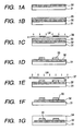
- Figs. 1A, 1B, 1C, 1D, 1E, 1F and 1G show the most preferable process flow in which a thermal crosslinkable positive resist is applied as a lower layer resist.
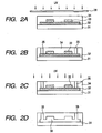
- Figs. 2A, 2B, 2C and 2D show a subsequent process following the process of Figs. 1A to 1G .
- a thermal crosslinkable positive resist layer 32 is coated over a substrate 31 and then baked.
- the coating process is performed by a solvent coating method such as spin coating or bar coating known in prior art.
- the baking process is preferably performed for 30 minutes to two hours at a baking temperature of 160 to 220°C at which a crosslinking reaction is carried out.
- a positive resist layer 33 having PMIPK as a primary component is coated over the upper layer of the thermal crosslinkable positive resist, and then is free-baked.
- the lower layer is known to be slightly dissolved by a coating solvent in the PMIPK coating process on the upper layer to form an compatible layer.
- the composition according to the present invention is crosslinkable, thereby not forming the compatible layer at all.
- a cold mirror exposing a PMIPK layer, which is the positive resist layer 33, and reflecting a wavelength of near 290 nm well.
- a mask aligner UX-3000SC commercially available by Ushio Denki Kabushiki Kaisha
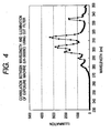
- a cut filter for cutting off light of less than 260 nm in front of an integrator including a fly-eye lens it is possible to permeate only the light of 260 to 330 nm which is a second wavelength band, as shown in Fig. 4 .
- a photosensitive wavelength band of photosensitive material in the present invention means a wavelength region which a polymer of main chain cleavage type absorbs the light and is changed into its excited state by irradiation of ionizing radiation within the upper or lower limits of wavelengths, thereby breaking the main chain thereof.
- a high molecular polymer is turned into a low molecular polymer and the solubility to the developing solution increases during the developing process to be described later.
- the upper resist layer 33 is developed and, during the development process, methylisobutyl ketone, which is a developing solution for PMIPK, is preferably used.
- methylisobutyl ketone which is a developing solution for PMIPK
- anything that dissolves an exposed portion of PMIPK and does not dissolve an unexposed portion will be applicable as the solvent according to the present invention.
- the substrate including the pattern layer of PMIPK is post-baked for 1 to 5 minutes at 100 to 120°C.
- a slope can be formed at a side face of the pattern according to temperature, time and pattern size, and an angle thereof can also be controlled by these parameters.
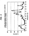
- a thermal crosslinkable positive resist layer 32 of the lower layer is exposed. This exposure is carried out by using light at 210 to 330 nm which is the first wavelength band as shown in Fig. 5 without using the above-described cut filter. At this time, the PMIPK of the upper layer is not sensitive to light because light is not irradiated by a photomask 37.
- the thermal crosslinkable positive resist layer 32 is developed.
- the development is carried out by methylisobutyl ketone.
- the developing solution is the same as the developing solution of the PMIPK of the upper layer, thereby the effect of the developing solution to the upper layer pattern can be eliminated.
- a liquid flow path forming material 34 is coated over the thermal crosslinkable positive resist layer 32 of the lower layer and the positive resist layer 33 of the upper layer.
- the coating process is carried out by a solvent coating method such as a general spin coating method well known in the prior art.
- the liquid flow path forming material is a material having onium salt as a primary component generating cations by epoxy resin of solid state and light irradiation at an ambient temperature, and has a negative property.
- Fig. 2A shows a process of performing light irradiation to the liquid flow path forming material
- a photomask 38 is adapted which does not irradiate light to a portion forming an ink discharge port.
- the pattern development of an ink discharge port 35 is carried out with respect to a photosensitive liquid flow path forming material 34.
- the photosensitive liquid flow path forming material is preferably developed by an aromatic solvent, such as xylene that does not dissolve PMIPK.
- an aromatic solvent such as xylene that does not dissolve PMIPK.
- such purpose is achieved by forming a photosensitive water repellent layer and carrying out exposure and development at the same time. At this time, the formation of the photosensitive water repellent layer may be carried out by means of lamination process.
- ionizing radiation of less than 300 nm over the liquid flow path forming material layer is entirely irradiated for a purpose of decomposing PMIPK or crosslinking resist into low molecules and easily removing them.
- the height of the liquid flow path can be varied from an ink supply hole to a heater.
- the optimization of the shape of the liquid flow path from the ink supply hole to the discharge chambers can reduce a crosstalk between the discharge chambers, as well as to be closely related to a speed of refilling ink to the discharge chambers.
- U.S. Patent No. 4,882,595 invented by Trueba and et al discloses the two-dimensional characteristic of a liquid flow path formed of photosensitive resist on a substrate, i.e., the shape in a direction parallel to the substrate, and the aforementioned characteristic.
- Japanese Patent Application Laid-Open No. 10-291317 invented by Murthy and et al discloses the changing of the height of a liquid flow path by processing a liquid flow path structure plate made of resin in a three-dimensional direction of interplanar and height directions.
- the method according to the present invention comprises a prior known solvent coating method such as spin coating used in semiconductor manufacturing techniques, so the liquid flow path can be formed stably with a very high precision.
- a two-dimensional shape in a direction parallel to the substrate is also formed by using the photolithography technique of a semiconductor, thereby it is possible to achieve a precision of submicrons unit.
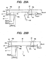
- the head produced according to a first example of using the present invention is featured in that the height of a liquid flow path from the end 42a of an ink supply hole 44 to discharge chambers 47 becomes smaller at the portion adjacent to the discharge chambers 47.
- Fig. 6B shows another liquid flow path shape for comparison.
- the speed of refilling ink to the discharge chambers 47 becomes higher since, the higher the height of the liquid flow path from the ink supply hole 42 to the discharge chambers 47 becomes, the lower the flow resistance of ink becomes.
- a discharge pressure is emitted to the ink supply hole 42 too, thereby degrading energy efficiency or increasing crosstalk between the discharge chambers 47.
- the height of the liquid flow path is designed in consideration of the aforementioned both characteristics.
- this method it is possible to change the height of the liquid flow path and achieve a liquid flow path shape of Fig. 6A .
- This head degrades the flow resistance of ink and enable refilling at a high speed by increasing the height of the liquid flow path from the ink supply hole 42 up to near the discharge chambers 47.
- the portions near the discharge chambers 47 have a configuration to suppress the energy generated from the discharge chambers 47 from being emitted to the ink supply hole 42 and prevent crosstalk by decreasing the height of the liquid flow path.
- a dust capture member hereinafter, referred to as "nozzle filter”
- nozzle filter a dust capture member of a column shape
- a nozzle filter 58 has such a shape that it does not reach to a substrate 51.
- Fig. 7B shows the configuration of a nozzle filter 59 for comparison.
- the ink discharge port of an ink jet head for achieving high image quality recording is very small and the nozzle filters are not formed, dusts and the like block the liquid flow path or the discharge port, thereby noticeably degrading the reliability of the ink jet head.
- the area of the liquid flow path can be maximized while making the interval between adjacent nozzles filters same as conventional one, thereby reducing the increase of the flow resistance of ink and capturing dusts. Consequently, even if the nozzle filter of a column shape is installed in the liquid flow path, the height of the liquid flow path can be changed so that the flow resistance of ink cannot be increased.
- the distance between adjacent filters is preferably less than 10 ⁇ m. More preferably, the columns forming these nozzle filters are configured not to reach to the substrate 51 as shown in Fig. 7A , thereby increasing the sectional area of the flow path.
- the head produced according to a third example of using the present invention is featured in that the height of a liquid flow path made of liquid flow path forming material 65 corresponding to the center portion of an ink supply hole 62 is lower than that of a liquid flow path corresponding to an opening circumferential portion 62b of the ink supply hole 62.
- Fig. 8B shows a liquid flow path shape as compared with the third embodiment.
- the aforementioned bad effect can be avoided by thickening the liquid flow path 65 corresponding to almost the overall opening of the ink supply hole 62 and increasing the height of the flow path only on the portion corresponding to the portions near the opening circumferential portion 62b of the ink supply hole 62 required for supplying ink.
- the distance from the ink supply hole opening circumferential portion 62b to the portion on which the height of the flow path is made higher by the liquid flow path forming material 65 is determined according to a discharge amount of an ink jet head to be designed or an ink viscosity, preferably, 10 to 100 ⁇ m in general.
- a discharge port of a discharge chamber 77 has a convex sectional shape.
- Fig. 9B shows a discharge port shape of another discharge chamber for comparison.
- the discharge energy of ink is greatly changed by the flow resistance of ink defined by the shape of a discharge port of the upper portion of a heater.
- the shape of a discharge shape is formed by patterning a liquid flow path forming material, thus it becomes a shape on which a discharge port pattern formed on a mask is projected.
- a discharge port is penetrated through the liquid flow path forming material layer and formed with the same area to the opening of a discharge port of the surface of the liquid flow path forming material.
- a discharge port of the discharge chamber 77 can be formed in a convex shape by changing the shape of the pattern of the upper layer material and the lower layer material. This is effective to increase ink discharge speed, increase the forwarding property of ink and provide a recording head capable of carrying out the recording process with a higher quality.
- Figs. 10 to 19 show an example of the construction and the production steps of a liquid jet recording head as obtainable through the present invention, respectively.
- the liquid jet recording head has two orifices (discharge ports) is disclosed in this example, it will be understood to those skilled in related art that the construction and the production process may be applied to the case of a high density multi-array liquid-jet recording head having two or more orifices.
- Figs. 10 to 19 schematically show the correlation of a first positive photosensitive material layer and a second positive photosensitive material layer regarding these essential portions. Other additional structures are not specially described herewith.
- a substrate 201 employed is made of glass, ceramic, plastic, metal, or the like as shown in Fig. 10 which is a schematic perspective view of a substrate before formation of a photosensitive material layer.
- the substrate 201 is not specially limited in its shape, material, and so forth, provided that it is capable of being a part of the liquid flow path forming materials and capable of acting as a supporting member to support the liquid flow path forming material composed of the photosensitive material layer, which will be described later.
- Plural liquid discharge energy generation elements 202 such as electrothermal transducers, piezoelectric elements, or the like are provided as desired on the substrate 201 (two elements in Fig. 10 ).
- the liquid discharge energy generation elements 202 apply energy to an ink to discharge recording liquid droplets and conduct recording process.
- an electrothermal transducer employed as the discharge energy generating element 202 heats the recording liquid around it to apply discharging energy; and a piezoelectric element employed as the discharge energy generation element 202 generates the discharging energy by mechanical vibration of the element.
- control signal input electrodes (not shown in the drawings) are connected to drive the elements.
- the element has a functional layer such as a protecting layer to improve durability of the discharge energy generation elements 202.
- a functional layer may naturally be provided without inconvenience.
- silicon is employed as the substrate 201. That is, since a driver or logic circuit for controlling a discharge energy generating element is produced by a general semiconductor production method, silicon is preferably applied to the substrate.
- silicon is preferably applied to the substrate.
- techniques such as YAG laser working or sand blasting may be employed.
- a prebaking temperature of this resist is very high as described above and exceeds a glass transition temperature of resin by a great extent, thereby making a resin coating fall into the through hole during prebaking.
- anisotropic etching technique of silicon by an alkali solution can be applied.
- a mask pattern is formed on the back surface of the substrate using an alkali resistant silicon nitride, and a membrane film forming an etching stopper is formed on the surface of the front substrate using the same material.
- a crosslinkable positive type resist layer 203 is formed on the substrate 201 containing the liquid discharge energy generation element 202.
- This material is a copolymer composed of methyl methacrylate, methacrylic acid and methacrylate anhydride in a ratio of 70:15:15.
- P(MMA-MAA-MAN) which is a thermally crosslinkable positive resist forming a lower layer has an absorption sensitivity around a region of 210 to 260 nm
- PMIPK which is a positive resist forming an upper layer has an absorption sensitivity around a region of 260 to 330 nm.
- a convex pattern of resist can be formed by selectively changing a wavelength band upon exposure.
- These resin particles are dissolved in cyclohexanone at a concentration of 30 wt% and then is used as a resist solution.
- This resist solution is spreading over the above-mentioned substrate 201 to coat it, prebaked in an oven for 60 minutes at 200°C and then thermally crosslinked.
- the obtained resist film had a thickness of 10 ⁇ m.
- ternary copolymer examples include:
- references examples of a ternary copolymer outside the scope of the claimed invention include:
- a positive type resist layer 204 of PMIPK is coated over the thermally crosslinkable positive resist layer 203.
- PMIPK ODUR-1010 (produced by Tokyo Ohka Kogyo Co., Ltd.) is used after being adjusted to have a resin concentration of 20 wt%. Prebaking is carried out on a hot plate for six minutes at 120°C. The obtained resin film had a thickness of 10 ⁇ m.
- the exposure of the positive resist layer 204 of PMIPK is conducted by any commonly available exposure apparatus.
- the apparatus used in the present invention is a deep UV exposure apparatus, UX-3000SC, produced by Ushio Electric Co., and is mounted with a cut filter for cutting off light of 260 nm or less as shown in Fig. 3 , and then the exposure is conducted in a 260 to 330 nm band region which is same to the second wavelength band as shown in Fig. 4 .
- An exposure amount is 10 J/cm 2 .
- the exposure is conducted through a photomask 206 drawing a pattern for leaving ionizing radiation 205 to the PMIPK.
- the development of the positive resist layer 204 of PMIPK is conducted to form a pattern.
- the development is conducted by immersing the resist layer in methylisobutylketone for one minute.
- the patterning process (exposure, development) of the lower thermally crosslinkable positive resist layer 203 is carried out.
- the same exposure apparatus as stated above is used and the patterning is conducted in a 210 to 330 nm band region which is the same first wavelength region as shown in Fig. 5 .
- An exposure amount is 35 J/cm 2 .
- Development is carried out with methylisobutyl ketone. The exposure is conducted through a photomask (not shown) drawing a pattern for leaving ionizing radiation to the thermally crosslinkable positive resist.
- a layer of liquid flow path forming material 207 is formed.
- the material of this layer is produced by dissolving 50 parts by weight of EHPE-3150 commercially available by Daicel Chemical Industries, Ltd., one part by weight of Photocation polymerization initiator SP-172 produced by Asahi Denka Co., Ltd. and 2.5 parts by weight of silane coupling agent A-187 commercially available by Nihonunica Corporation in 50 parts by weight of xylene used as a coating solvent.
- the coating is conducted by spin coating and prebaking is conducted on a hot plate for three minutes at 90°C.
- conducted is the pattern exposure and development of an ink discharge port 209.
- This pattern exposure may be conducted by any one of general exposure apparatuses. Though not shown in the drawings, a mask is used during exposure which does not irradiate light to the portion forming the ink discharge port.
- the exposure is conducted with a Canon MPA-600 Super mask aligner, with an exposure dose of 500 mJ/cm 2 .
- the development is conducted by immersing in xylene for 60 seconds. Afterwards, one hour baking is conducted at 100°C to increase the contactability of the liquid flow path forming material.
- the liquid flow path forming material layer is coated with a cyclic isoprene to protect this material layer from an alkali solution.
- a cyclic isoprene manufactured and sold by Tokyo Ohka Kogyo Co., Ltd. under a trade name of OBC is used.
- the silicon substrate is immersed in a 22 wt% tetramethyl ammonium hydroxide (TMAH) solution for 14.5 hours at 83°C, and a through hole (not shown) for supplying ink is formed.
- TMAH tetramethyl ammonium hydroxide
- silicon nitride used as a mask and a membrane is previously patterned on the silicon substrate to form an ink supply opening.
- the silicon substrate is mounted to a dry etching device in such a manner that the back surface can be upside, and the membrane film is removed by an etchant made by mixing 5% oxygen to CF 4 .
- the silicon substrate is immersed in xylene to remove the OBC.
- ionizing radiation 208 of 210 to 330 nm region band entirely irradiates to the liquid flow path forming material 207 using a low temperature mercury. Then, the upper positive resist layer of PMIPK and the lower thermally crosslinkable positive resist layer are decomposed. An irradiation dose is 81 J/cm 2 .
- the substrate 201 is immersed in lactic acid methyl to remove the resist pattern in overall as shown in the vertical sectional view of Fig. 18 .
- the substrate 201 is put into a megasonic bath of 200 MHz to promote a decrease in dissolution time period.
- liquid flow paths 211 including discharge chambers are formed, and ink is introduced into each of the discharge chambers via each liquid flow path 211 from an ink supply opening 210, thereby producing an ink discharge element having a structure of discharging ink from a discharge port 209 by a heater.
- the produced discharge element is mounted on an ink jet head unit of such a shape as shown in Fig. 19 .
- the above-mentioned ink jet head unit has such a construction, for example, that a TAB film 214 for transmitting and receiving a recording signal to/from a recording apparatus main body is formed on the outer surface of a supporting member for detachably supporting the ink tank 213.
- An ink discharge element 212 on the TAB film 214 is connected to an electric wire by an electric connecting lead 215.
- an ink jet head having a structure as shown in Fig. 6A is produced.
- the ink jet head has a horizontal distance of 100 ⁇ m from an opening circumferential portion 42a of an ink supply opening 42 to one end 47a of the ink supply opening of the discharge chamber 47.
- a liquid flow path wall 46 is formed to the portion having a distance of 60 ⁇ m from the end 47a of the ink supply opening of the discharge chamber 47, and divides the discharge elements into each.
- the height of the liquid flow path is 10 ⁇ m from the end 47a of the ink supply opening of the discharge chamber 47 to the ink supply opening 42, and the height of the other portions is 20 ⁇ m.
- the distance from the surface of the substrate 41 to the surface of the liquid flow path forming material 45 is 26 ⁇ m.
- Fig. 20B shows a cross section of a flow path of an ink jet head according to a conventional method. This head has a liquid flow path height of 15 ⁇ m throughout the overall areas.
- a flow path structure of Fig. 20A shows a refill speed of 45 ⁇ sec.
- a flow path structure of Fig. 20B shows a refill speed of 25 ⁇ sec.
- a head having a nozzle filter as shown in Fig. 7A is manufactured for trial.
- a nozzle filter 58 is configured by forming columns with a diameter of 3 ⁇ m at a portion spaced 20 ⁇ m from the opening circumferential portion of an ink supply opening 52 toward discharge chambers 57.
- the gap between the columns constituting the nozzle filter is 10 ⁇ m.
- a nozzle filter 59 according to a conventional method as shown in Fig. 7B has the same location and shape but is different from the nozzle filter of this example since it reaches up to the substrate 51.
- a filter structure of Fig. 7A shows a refill speed of 58 ⁇ sec and a filter structure of Fig. 7B shows a refill speed of 65 ⁇ sec. According to the ink jet head according to this example, it is turned out that the refill time of ink can be reduced.
- an ink jet head having a structure as shown in Fig. 8A is manufactured for trial.
- a liquid flow path corresponding to an ink supply opening 62 has a height of 30 ⁇ m from an opening circumferential portion 62b of an ink supply opening 62 toward the center portion of the supply opening.
- the layer thickness of a liquid flow path forming material 65 is 6 ⁇ m. Besides this portion, in the height of the liquid flow path corresponding to the ink supply opening 62, the layer thickness of the liquid flow path forming material 65 is 16 ⁇ m.
- the ink supply opening 62 has a width of 200 ⁇ m and a length of 14 mm.
- the layer thickness of the portion corresponding to the ink supply opening 62 of the liquid flow path forming material 65 is 6 ⁇ m.
- each of the heads of Figs. 8A and 8B are manufactured for trial, and a drop test of the heads is conducted at a height of 90 cm.
- the head structure of Fig. 8B shows a crack occurrence on the liquid flow path structure material 65 in 9 of 10 heads, while the head structure of Fig. 8A shows no crack in any of 10 heads.
- an ink jet head having a structure as shown in Fig. 9A is manufactured for trial.
- discharge chambers 77 are constructed in such a manner that a rectangular portion made of a lower layer resist is a 25 ⁇ m square having a height of 10 ⁇ m, a rectangular portion made of an upper layer resist is a 20 ⁇ m square having a height of 10 ⁇ m and a discharge port is a round hole having a diameter of 15 ⁇ m.
- the distance from the heater 73 to the opening surface of the discharge port 74 is 26 ⁇ m.
- Fig. 21B shows a sectional shape of a discharge port of a head according to a conventional method.
- the discharge chamber is a rectangular in which one side is 20 ⁇ m and a height is 20 ⁇ m.
- the discharge port 74 is formed of a round hole having a diameter of 15 ⁇ m.
- the head as shown in Fig. 21A has a discharge amount of 3ng, a discharge speed of 15 m/sec and an impact precision of 3 ⁇ m at a position spaced 1 mm from the discharge port 74 in a discharge direction.
- the head as shown in Fig. 21B has a discharge amount of 3 ng, a discharge speed of 9 m/sec and an impact precision of 5 ⁇ m.
- a substrate 201 is prepared. Most generally, as the substrate 201, a silicon substrate is applied. Generally, a driver or logic circuit for controlling a discharge energy generation element is produced by a general semiconductor manufacture method, silicon is preferably applied to this substrate. In this background example, there is prepared an electrothermal converting element (heater made of HfB 2 material) as an ink discharge pressure generation element 202 and a silicon substrate having an ink flow path and a lamination film (not shown) of SiN+Ta on a nozzle forming portion ( Fig. 2 ).
- a first positive resist layer 203 is formed on the substrate ( Fig. 2 ) including the ink discharge pressure generation element 202.
- the first positive resist the following photodegradation type positive resists are used.
- This resin powder is dissolved in cyclohexanone at a solids concentration of about 30 wt% and is used as a resist solution.
- the viscosity of the resist solution is 630 cps.
- This resist solution is coated by spin coating, prebaked for three minutes at 120°C and heat treated under a nitrogen atmosphere in an oven for 60 minutes at 250°C.
- the film thickness of the resist layer after the heat treatment is 10 ⁇ m.
- a first positive resist layer 204 polymethyl isopropenyl ketone (ODUR produced by Tokyo Oka Co.) is spin coated and baked for three minutes at 120°C.
- the film thickness of the resist layer after the baking is 10 ⁇ m.
- the patterning of a second positive resist layer is conducted.
- a deep UV exposure apparatus UX-3000SC, manufactured by Ushio Electric Co. is used, and is mounted with a cut filter for cutting off light of 260 nm or less.
- the pattern is exposed at an exposure does of 3,000 mJ/cm 2 , developed with methylisobutylketone, rinsed with isopropyl alcohol to form a second flow path pattern.
- the patterning of the first positive resist layer is conducted.
- an optical filter for cutting off the light of a wavelength of more than 270 nm is mounted.
- the pattern is exposed at an exposure does of 10,000 mJ/cm 2 , developed with the following developing solution, rinsed with isopropyl alcohol to form a second flow path pattern.
- Developing solution Diethylenglycolmonobutylether 60 vol% Ethanolamine. 5 vol% Morpholine 20 vol% Ion exchange water 15 vol%
- a photosensitive resin composition composed of the following compositions (film thickness: 20 ⁇ m on a flat plate) and baked on a hot plate for two minutes at 100°C to form a liquid flow path forming material 207.
- EHPE produced by Daicel Chemical Ind., Ltd.
- 1,4-HFAB produced. by Central Glass Co., Ltd.
- SP-170 produced by Asahi Denka Kogyo K.K.
- A-187 produced by Nippon Unicar Co., Ltd.
- Methylisobutylketone 100 parts by weight Diglyme 100 parts by weight
- a photosensitive resin composition composed of the following compositions is coated by spin coating to have a film thickness of 1 ⁇ m and baked on a hot plate for three minutes at 80°C to form an ink-repellent agent layer.
- EHPE-3158 (produced by Daicel Chemical Ind., Ltd.) 35 parts by weight 2,2-bis(4-glycidyloxyphenyl )hexafluoropropane 25 parts by weight 1,4-bis(2-hydroxyhexafluoroisopropyl)benzene 25 parts by weight 3-(2-perfluorohexyl)ethoxy-1,2-epoxypropane 16 parts by weight A-187 (produced by Nippon Unicar Co., Ltd.) 4 parts by weight SP-170 (produced by Asahi Denka Kogyo K.K.) 2 parts by weight Diethyleneglycol monoethylether 100 parts by weight
- the pattern is exposed with an exposure dose of 400 mJ/cm 2 .
- PEB is conducted on a hot plate for 120 seconds at 120°C and development is carried out with methylisobutylketone.
- the pattern of a liquid flow path forming material 207 and an ink-repellent agent layer 8 is conducted and an ink discharge port 209 is formed.
- a discharge port pattern of ⁇ 10 ⁇ m is formed.
- a polyetheramide resin composition HIMAL manufactured by Hitachi Chemical Co., Ltd.
- HIMAL manufactured by Hitachi Chemical Co., Ltd.
- an etching mask having an opening portion with a 1 mm width and a 10 mm length is created.
- the processed substrate is immersed in a TMAH aqueous solution of 22 wt% maintained at 80°C, and an ink supply opening 210 is formed.
- a protective layer OBC (commercially available by Tokyo Oka Co.: not shown) is coated on the ink-repellent agent layer 8 to perform anisotropic etching.
- the OBC used as the protective layer is dissolved and removed using xylene.
- the overall exposure is conducted with an exposure dose of 50,000 mJ/cm 2 over a nozzle forming member and the ink-repellent agent layer without mounting an optical filter, and flow path patterns 5 and 6 are solubilized.
- a liquid discharge ink jet head is created.
- the polyetheramide resin composition layer used as an etching mask is removed by dry etching using oxygen plasma.
- the resultant produced ink jet head is mounted on a printer and the evaluation of discharging and recording is conducted. As a result, a good image recording can be performed.
Applications Claiming Priority (4)
| Application Number | Priority Date | Filing Date | Title |
|---|---|---|---|
| JP2002201971 | 2002-07-10 | ||
| JP2002201971 | 2002-07-10 | ||
| JP2003271623A JP4280574B2 (ja) | 2002-07-10 | 2003-07-07 | 液体吐出ヘッドの製造方法 |
| JP2003271623 | 2003-07-07 |
Publications (2)
| Publication Number | Publication Date |
|---|---|
| EP1380425A1 EP1380425A1 (en) | 2004-01-14 |
| EP1380425B1 true EP1380425B1 (en) | 2011-02-02 |
Family
ID=29738476
Family Applications (1)
| Application Number | Title | Priority Date | Filing Date |
|---|---|---|---|
| EP03015760A Expired - Lifetime EP1380425B1 (en) | 2002-07-10 | 2003-07-10 | Method of producing microstructure, and method of producing liquid discharge head |
Country Status (7)
| Country | Link |
|---|---|
| US (1) | US6986980B2 (ko) |
| EP (1) | EP1380425B1 (ko) |
| JP (1) | JP4280574B2 (ko) |
| KR (1) | KR100591654B1 (ko) |
| CN (1) | CN1257059C (ko) |
| DE (1) | DE60335931D1 (ko) |
| TW (1) | TWI221122B (ko) |
Families Citing this family (29)
| Publication number | Priority date | Publication date | Assignee | Title |
|---|---|---|---|---|
| FR2849222B1 (fr) * | 2002-12-20 | 2005-10-21 | Commissariat Energie Atomique | Microstructure comportant une couche d'adherence et procede de fabrication d'une telle microstructure |
| DE10353767B4 (de) * | 2003-11-17 | 2005-09-29 | Infineon Technologies Ag | Vorrichtung zur Häusung einer mikromechanischen Struktur und Verfahren zur Herstellung derselben |
| DE10361075A1 (de) * | 2003-12-22 | 2005-07-28 | Pac Tech - Packaging Technologies Gmbh | Verfahren und Vorichtung zur Trocknung von Schaltungssubstraten |
| JP4761498B2 (ja) * | 2004-06-28 | 2011-08-31 | キヤノン株式会社 | 感光性樹脂組成物、ならびにこれを用いた段差パターンの製造方法及びインクジェットヘッドの製造方法 |
| CN1977219B (zh) * | 2004-06-28 | 2011-12-28 | 佳能株式会社 | 制造微细结构的方法、制造排液头的方法以及排液头 |
| JP4484774B2 (ja) * | 2004-06-28 | 2010-06-16 | キヤノン株式会社 | 液体吐出ヘッドの製造方法 |
| DE602005022448D1 (de) * | 2004-06-28 | 2010-09-02 | Canon Kk | Ekopfs und unter verwendung dieses verfahrens erhaltener flüssigkeitsausgabekopf |
| JP4533256B2 (ja) * | 2004-06-28 | 2010-09-01 | キヤノン株式会社 | 微細構造体の製造方法および液体吐出ヘッドの製造方法 |
| CN100496984C (zh) * | 2004-06-28 | 2009-06-10 | 佳能株式会社 | 排液头的制造方法和使用这一方法获得的排液头 |
| JP4447974B2 (ja) * | 2004-06-28 | 2010-04-07 | キヤノン株式会社 | インクジェットヘッドの製造方法 |
| JP5027991B2 (ja) * | 2004-12-03 | 2012-09-19 | キヤノン株式会社 | インクジェットヘッドおよびその製造方法 |
| CN101316713B (zh) * | 2005-12-02 | 2011-03-30 | 佳能株式会社 | 液体排出头的制造方法 |
| US8438729B2 (en) * | 2006-03-09 | 2013-05-14 | Canon Kabushiki Kaisha | Method of producing liquid discharge head |
| US8376525B2 (en) * | 2006-09-08 | 2013-02-19 | Canon Kabushiki Kaisha | Liquid discharge head and method of manufacturing the same |
| JP2008290413A (ja) * | 2007-05-28 | 2008-12-04 | Canon Inc | 液体吐出ヘッドの製造方法 |
| US8039195B2 (en) * | 2008-02-08 | 2011-10-18 | Taiwan Semiconductor Manufacturing Company, Ltd. | Si device making method by using a novel material for packing and unpacking process |
| US8137573B2 (en) * | 2008-06-19 | 2012-03-20 | Canon Kabushiki Kaisha | Liquid ejection head, method for manufacturing liquid ejection head, and method for manufacturing structure |
| JP5069186B2 (ja) * | 2008-07-29 | 2012-11-07 | ソニー株式会社 | 液滴吐出ヘッド及び液滴吐出装置 |
| KR20100060423A (ko) * | 2008-11-27 | 2010-06-07 | 삼성전자주식회사 | 잉크젯 프린트헤드 및 그 제조방법 |
| US8499453B2 (en) * | 2009-11-26 | 2013-08-06 | Canon Kabushiki Kaisha | Method of manufacturing liquid discharge head, and method of manufacturing discharge port member |
| FR2953991B1 (fr) * | 2009-12-10 | 2012-01-06 | Commissariat Energie Atomique | Procede de realisation d'un revetement de surface controle tridimensionnellement dans une cavite |
| US11175279B2 (en) | 2010-05-03 | 2021-11-16 | Creatv Microtech, Inc. | Polymer microfilters, devices comprising the same, methods of manufacturing the same, and uses thereof |
| WO2011139445A1 (en) * | 2010-05-03 | 2011-11-10 | Creatv Microtech, Inc. | Polymer microfilters and methods of manufacturing the same |
| US8434229B2 (en) * | 2010-11-24 | 2013-05-07 | Canon Kabushiki Kaisha | Liquid ejection head manufacturing method |
| US9308726B2 (en) * | 2012-02-16 | 2016-04-12 | Xerox Corporation | Printhead fluid paths formed with sacrificial material patterned using additive manufacturing processes |
| CN103252997B (zh) * | 2012-02-16 | 2015-12-16 | 珠海纳思达珠海赛纳打印科技股份有限公司 | 一种液体喷头及其制造方法 |
| US9599852B1 (en) * | 2013-08-05 | 2017-03-21 | Lensvector, Inc. | Manufacturing of liquid crystal lenses using carrier substrate |
| CN106716257B (zh) | 2014-09-30 | 2019-12-24 | 富士胶片株式会社 | 图案形成方法、抗蚀剂图案及电子元件的制造方法 |
| KR20230047461A (ko) * | 2020-09-07 | 2023-04-07 | 후지필름 가부시키가이샤 | 경화물의 제조 방법, 적층체의 제조 방법, 및, 전자 디바이스의 제조 방법 |
Family Cites Families (21)
| Publication number | Priority date | Publication date | Assignee | Title |
|---|---|---|---|---|
| CA969692A (en) | 1969-09-15 | 1975-06-17 | Richard A. Jones | Catalysed thermosetting polymeric coatings and inks |
| DE3540480A1 (de) * | 1985-11-15 | 1987-05-21 | Hoechst Ag | Durch strahlung polymerisierbares gemisch, daraus hergestelltes aufzeichnungsmaterial und verfahren zur herstellung von reliefaufzeichnungen |
| US4882595A (en) | 1987-10-30 | 1989-11-21 | Hewlett-Packard Company | Hydraulically tuned channel architecture |
| US4835086A (en) * | 1988-02-12 | 1989-05-30 | Hoechst Celanese Corporation | Polysulfone barrier layer for bi-level photoresists |
| US4906552A (en) * | 1988-02-22 | 1990-03-06 | Hughes Aircraft Company | Two layer dye photoresist process for sub-half micrometer resolution photolithography |
| JPH0631444B2 (ja) | 1989-06-07 | 1994-04-27 | 東洋鋼板株式会社 | 半田用複層めっき鋼板 |
| JPH0740808B2 (ja) | 1990-10-17 | 1995-05-10 | 井関農機株式会社 | トラクターの油圧昇降制御装置 |
| DE69127801T2 (de) * | 1990-12-19 | 1998-02-05 | Canon Kk | Herstellungsverfahren für flüssigkeitsausströmenden Aufzeichnungskopf |
| JP2694054B2 (ja) | 1990-12-19 | 1997-12-24 | キヤノン株式会社 | 液体噴射記録ヘッド、その製造方法、及び液体噴射記録ヘッドを備えた記録装置 |
| JPH0645242A (ja) | 1992-07-24 | 1994-02-18 | Hitachi Ltd | レジスト塗布方法及びその装置 |
| JP3143307B2 (ja) | 1993-02-03 | 2001-03-07 | キヤノン株式会社 | インクジェット記録ヘッドの製造方法 |
| EP0715957B1 (en) | 1994-12-05 | 1999-05-26 | Canon Kabushiki Kaisha | Process for the production of an ink jet head |
| DE69603639T2 (de) * | 1995-03-31 | 2000-04-13 | Canon Kk | Verfahren zum Herstellen eines Tintenstrahlkopfes |
| US6113214A (en) * | 1995-06-08 | 2000-09-05 | Canon Kabushiki Kaisha | Ink jet recording head having components made from the same material, recording apparatus using the head, and method for manufacturing such head and ink jet recording apparatus |
| US6158843A (en) | 1997-03-28 | 2000-12-12 | Lexmark International, Inc. | Ink jet printer nozzle plates with ink filtering projections |
| JP3373147B2 (ja) * | 1998-02-23 | 2003-02-04 | シャープ株式会社 | フォトレジスト膜及びそのパターン形成方法 |
| JP4497633B2 (ja) | 1999-03-15 | 2010-07-07 | キヤノン株式会社 | 撥液体層の形成方法及び液体吐出ヘッドの製造方法 |
| US6582890B2 (en) * | 2001-03-05 | 2003-06-24 | Sandia Corporation | Multiple wavelength photolithography for preparing multilayer microstructures |
| JP4532785B2 (ja) * | 2001-07-11 | 2010-08-25 | キヤノン株式会社 | 構造体の製造方法、および液体吐出ヘッドの製造方法 |
| JP2003300323A (ja) * | 2002-04-11 | 2003-10-21 | Canon Inc | インクジェットヘッド及びその製造方法 |
| JP2004042389A (ja) * | 2002-07-10 | 2004-02-12 | Canon Inc | 微細構造体の製造方法、液体吐出ヘッドの製造方法および液体吐出ヘッド |
-
2003
- 2003-07-07 JP JP2003271623A patent/JP4280574B2/ja not_active Expired - Fee Related
- 2003-07-09 US US10/615,302 patent/US6986980B2/en not_active Expired - Fee Related
- 2003-07-10 CN CNB031467830A patent/CN1257059C/zh not_active Expired - Fee Related
- 2003-07-10 EP EP03015760A patent/EP1380425B1/en not_active Expired - Lifetime
- 2003-07-10 TW TW092118905A patent/TWI221122B/zh not_active IP Right Cessation
- 2003-07-10 KR KR1020030046719A patent/KR100591654B1/ko not_active IP Right Cessation
- 2003-07-10 DE DE60335931T patent/DE60335931D1/de not_active Expired - Lifetime
Also Published As
| Publication number | Publication date |
|---|---|
| CN1257059C (zh) | 2006-05-24 |
| TWI221122B (en) | 2004-09-21 |
| US6986980B2 (en) | 2006-01-17 |
| TW200401714A (en) | 2004-02-01 |
| EP1380425A1 (en) | 2004-01-14 |
| JP2004046217A (ja) | 2004-02-12 |
| DE60335931D1 (de) | 2011-03-17 |
| KR100591654B1 (ko) | 2006-06-20 |
| JP4280574B2 (ja) | 2009-06-17 |
| CN1475350A (zh) | 2004-02-18 |
| KR20040005695A (ko) | 2004-01-16 |
| US20040131957A1 (en) | 2004-07-08 |
Similar Documents
| Publication | Publication Date | Title |
|---|---|---|
| EP1380425B1 (en) | Method of producing microstructure, and method of producing liquid discharge head | |
| JP4532785B2 (ja) | 構造体の製造方法、および液体吐出ヘッドの製造方法 | |
| US6951380B2 (en) | Method of manufacturing microstructure, method of manufacturing liquid discharge head, and liquid discharge head | |
| EP1768848B1 (en) | Liquid discharge head manufacturing method, and liquid discharge head obtained using this method | |
| EP1768847B1 (en) | Liquid discharge head manufacturing method, and liquid discharge head obtained using this method | |
| EP1766475B1 (en) | Method of forming level difference pattern using the photosensitive resin composition, and method of producing ink jet head | |
| JP5159823B2 (ja) | 構造体の製造方法および液体吐出ヘッドの製造方法 | |
| US7592131B2 (en) | Method for producing fine structured member, method for producing fine hollow structured member and method for producing liquid discharge head | |
| JP4533256B2 (ja) | 微細構造体の製造方法および液体吐出ヘッドの製造方法 | |
| JP2004042396A (ja) | 微細構造体の製造方法、液体吐出ヘッドの製造方法および液体吐出ヘッド | |
| KR20070022805A (ko) | 액체 토출 헤드 제조 방법, 및 이러한 방법을 사용하여얻어지는 액체 토출 헤드 | |
| JP2007130873A (ja) | インクジェット記録ヘッド及びその製造方法 |
Legal Events
| Date | Code | Title | Description |
|---|---|---|---|
| PUAI | Public reference made under article 153(3) epc to a published international application that has entered the european phase |
Free format text: ORIGINAL CODE: 0009012 |
|
| AK | Designated contracting states |
Kind code of ref document: A1 Designated state(s): AT BE BG CH CY CZ DE DK EE ES FI FR GB GR HU IE IT LI LU MC NL PT RO SE SI SK TR |
|
| AX | Request for extension of the european patent |
Extension state: AL LT LV MK |
|
| 17P | Request for examination filed |
Effective date: 20040714 |
|
| AKX | Designation fees paid |
Designated state(s): DE FR GB IT |
|
| 17Q | First examination report despatched |
Effective date: 20051118 |
|
| GRAP | Despatch of communication of intention to grant a patent |
Free format text: ORIGINAL CODE: EPIDOSNIGR1 |
|
| RTI1 | Title (correction) |
Free format text: METHOD OF PRODUCING MICROSTRUCTURE, AND METHOD OF PRODUCING LIQUID DISCHARGE HEAD |
|
| GRAS | Grant fee paid |
Free format text: ORIGINAL CODE: EPIDOSNIGR3 |
|
| GRAA | (expected) grant |
Free format text: ORIGINAL CODE: 0009210 |
|
| AK | Designated contracting states |
Kind code of ref document: B1 Designated state(s): DE FR GB IT |
|
| REG | Reference to a national code |
Ref country code: GB Ref legal event code: FG4D |
|
| REF | Corresponds to: |
Ref document number: 60335931 Country of ref document: DE Date of ref document: 20110317 Kind code of ref document: P |
|
| REG | Reference to a national code |
Ref country code: DE Ref legal event code: R096 Ref document number: 60335931 Country of ref document: DE Effective date: 20110317 |
|
| PLBE | No opposition filed within time limit |
Free format text: ORIGINAL CODE: 0009261 |
|
| STAA | Information on the status of an ep patent application or granted ep patent |
Free format text: STATUS: NO OPPOSITION FILED WITHIN TIME LIMIT |
|
| 26N | No opposition filed |
Effective date: 20111103 |
|
| REG | Reference to a national code |
Ref country code: DE Ref legal event code: R097 Ref document number: 60335931 Country of ref document: DE Effective date: 20111103 |
|
| GBPC | Gb: european patent ceased through non-payment of renewal fee |
Effective date: 20110710 |
|
| REG | Reference to a national code |
Ref country code: FR Ref legal event code: ST Effective date: 20120330 |
|
| PG25 | Lapsed in a contracting state [announced via postgrant information from national office to epo] |
Ref country code: FR Free format text: LAPSE BECAUSE OF NON-PAYMENT OF DUE FEES Effective date: 20110801 |
|
| PG25 | Lapsed in a contracting state [announced via postgrant information from national office to epo] |
Ref country code: IT Free format text: LAPSE BECAUSE OF FAILURE TO SUBMIT A TRANSLATION OF THE DESCRIPTION OR TO PAY THE FEE WITHIN THE PRESCRIBED TIME-LIMIT Effective date: 20110202 |
|
| PG25 | Lapsed in a contracting state [announced via postgrant information from national office to epo] |
Ref country code: GB Free format text: LAPSE BECAUSE OF NON-PAYMENT OF DUE FEES Effective date: 20110710 |
|
| PGFP | Annual fee paid to national office [announced via postgrant information from national office to epo] |
Ref country code: DE Payment date: 20150731 Year of fee payment: 13 |
|
| REG | Reference to a national code |
Ref country code: DE Ref legal event code: R119 Ref document number: 60335931 Country of ref document: DE |
|
| PG25 | Lapsed in a contracting state [announced via postgrant information from national office to epo] |
Ref country code: DE Free format text: LAPSE BECAUSE OF NON-PAYMENT OF DUE FEES Effective date: 20170201 |