EP1371088B1 - Metal gate stack with etch stop layer improved through implantation of metallic atoms and method of manufacturing the same - Google Patents
Metal gate stack with etch stop layer improved through implantation of metallic atoms and method of manufacturing the same Download PDFInfo
- Publication number
- EP1371088B1 EP1371088B1 EP02704371A EP02704371A EP1371088B1 EP 1371088 B1 EP1371088 B1 EP 1371088B1 EP 02704371 A EP02704371 A EP 02704371A EP 02704371 A EP02704371 A EP 02704371A EP 1371088 B1 EP1371088 B1 EP 1371088B1
- Authority
- EP
- European Patent Office
- Prior art keywords
- metal
- metal layer
- layer
- tin
- gate
- Prior art date
- Legal status (The legal status is an assumption and is not a legal conclusion. Google has not performed a legal analysis and makes no representation as to the accuracy of the status listed.)
- Expired - Lifetime
Links
Images


Classifications
-
- H—ELECTRICITY
- H10—SEMICONDUCTOR DEVICES; ELECTRIC SOLID-STATE DEVICES NOT OTHERWISE PROVIDED FOR
- H10D—INORGANIC ELECTRIC SEMICONDUCTOR DEVICES
- H10D64/00—Electrodes of devices having potential barriers
- H10D64/60—Electrodes characterised by their materials
- H10D64/66—Electrodes having a conductor capacitively coupled to a semiconductor by an insulator, e.g. MIS electrodes
- H10D64/667—Electrodes having a conductor capacitively coupled to a semiconductor by an insulator, e.g. MIS electrodes the conductor comprising a layer of alloy material, compound material or organic material contacting the insulator, e.g. TiN workfunction layers
-
- H—ELECTRICITY
- H10—SEMICONDUCTOR DEVICES; ELECTRIC SOLID-STATE DEVICES NOT OTHERWISE PROVIDED FOR
- H10D—INORGANIC ELECTRIC SEMICONDUCTOR DEVICES
- H10D64/00—Electrodes of devices having potential barriers
- H10D64/01—Manufacture or treatment
- H10D64/011—Manufacture or treatment of electrodes ohmically coupled to a semiconductor
-
- H—ELECTRICITY
- H10—SEMICONDUCTOR DEVICES; ELECTRIC SOLID-STATE DEVICES NOT OTHERWISE PROVIDED FOR
- H10D—INORGANIC ELECTRIC SEMICONDUCTOR DEVICES
- H10D64/00—Electrodes of devices having potential barriers
- H10D64/01—Manufacture or treatment
- H10D64/013—Manufacture or treatment of electrodes having a conductor capacitively coupled to a semiconductor by an insulator
- H10D64/01302—Manufacture or treatment of electrodes having a conductor capacitively coupled to a semiconductor by an insulator the insulator being formed after the semiconductor body, the semiconductor being silicon
- H10D64/01304—Manufacture or treatment of electrodes having a conductor capacitively coupled to a semiconductor by an insulator the insulator being formed after the semiconductor body, the semiconductor being silicon characterised by the conductor
- H10D64/01318—Manufacture or treatment of electrodes having a conductor capacitively coupled to a semiconductor by an insulator the insulator being formed after the semiconductor body, the semiconductor being silicon characterised by the conductor the conductor comprising a layer of alloy material, compound material or organic material contacting the insulator, e.g. TiN
-
- Y—GENERAL TAGGING OF NEW TECHNOLOGICAL DEVELOPMENTS; GENERAL TAGGING OF CROSS-SECTIONAL TECHNOLOGIES SPANNING OVER SEVERAL SECTIONS OF THE IPC; TECHNICAL SUBJECTS COVERED BY FORMER USPC CROSS-REFERENCE ART COLLECTIONS [XRACs] AND DIGESTS
- Y10—TECHNICAL SUBJECTS COVERED BY FORMER USPC
- Y10S—TECHNICAL SUBJECTS COVERED BY FORMER USPC CROSS-REFERENCE ART COLLECTIONS [XRACs] AND DIGESTS
- Y10S438/00—Semiconductor device manufacturing: process
- Y10S438/942—Masking
- Y10S438/947—Subphotolithographic processing
-
- Y—GENERAL TAGGING OF NEW TECHNOLOGICAL DEVELOPMENTS; GENERAL TAGGING OF CROSS-SECTIONAL TECHNOLOGIES SPANNING OVER SEVERAL SECTIONS OF THE IPC; TECHNICAL SUBJECTS COVERED BY FORMER USPC CROSS-REFERENCE ART COLLECTIONS [XRACs] AND DIGESTS
- Y10—TECHNICAL SUBJECTS COVERED BY FORMER USPC
- Y10S—TECHNICAL SUBJECTS COVERED BY FORMER USPC CROSS-REFERENCE ART COLLECTIONS [XRACs] AND DIGESTS
- Y10S438/00—Semiconductor device manufacturing: process
- Y10S438/942—Masking
- Y10S438/948—Radiation resist
- Y10S438/949—Energy beam treating radiation resist on semiconductor
Definitions
- the present invention relates to the field of semiconductor processing, and more particularly to the formation of metal gate electrodes.
- MOS transistors have typically been formed utilizing polysilicon gate electrodes.
- Polysilicon material has been preferred for use as an MOS gate electrode due to its thermal resistive properties (i.e., polysilicon can better withstand subsequent high-temperature processing).
- Polysilicon's robustness during high-temperature processing allows polysilicon to be annealed at high temperatures along with source and drain regions.
- polysilicon's ability to block the ion implantation of doped atoms into a channel region is advantageous. Due to the ion implantation blocking potential of polysilicon, polysilicon allows for the easy formation of self-aligned source and drain structures after gate patterning is completed.
- polysilicon gate electrodes have certain disadvantages.
- polysilicon gate electrodes are formed from semiconductor materials that suffer from higher resistivities than most metal materials. Therefore, polysilicon gate electrodes may operate at much slower speeds than gates made of metallic materials. To partially compensate for the high resistance, polysilicon materials often require extensive and expensive silicide processing in order to increase their speed of operation to acceptable levels.
- Metal gates are therefore being investigated as replacements for polysilicon gates.
- Metal gates are fabricated in a manner that is similar to the fabrication processes for polysilicon gates.
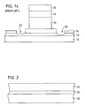
- An exemplary layer structure is depicted in Figure 1A of a metal gate structure.
- Gate oxide layer 12 is first deposited on a substrate 10.
- the layer 14 is primarily chosen for appropriate workfunction properties which determine the threshold voltage of the transistor structure.
- the barrier layer also aids in the adhesion of the subsequently formed metal gate.
- the TiN can be deposited by conventional methodologies, such as physical vapor deposition (PVD). Alternate materials such as TaN, TaSi x N y , WN etc. may be used for this purpose.
- a metal gate layer 16 is then formed on the barrier layer 14.
- An exemplary material for the metal gate layer 16 is tungsten, although other materials may be used. The tungsten is deposited by conventional methodologies
- a SiRN anti-reflective coating (ARC) 18 is formed on the metal gate layer 16. This is followed by formation of a cap layer 20 over the ARC layer 18.
- the cap layer 20 may comprise silicon nitride (SiN), for example.
- the anti-reflective coating 18 and the cap layer 20 aid in the patterning of the gate prior to the reactive ion etch process used to form the gate.
- Anti-reflective coatings 18, 20 increase the resolution during the lithography process.
- the metal gate is now etched. This is accomplished by conventional patterning and etching techniques.
- the tungsten layer is typically etched with a fluorine containing chemistry, such as SF6/N2 or SF6/Cl2/N2, with WF6 being the primary product species.
- a fluorine containing chemistry such as SF6/N2 or SF6/Cl2/N2
- WF6 being the primary product species.
- the latter chemistry has yielded good profiles.
- an appropriate SF6/C12 ratio may be chosen to provide the best profiles.
- the recipe may even be richer in Cl2 than in SF6 as required. It is desirable for the etchant to have good selectivity to the TiN of the barrier layer 14 so that the tungsten can be cleared across the entire wafer without attacking the gate oxide.
- the TiN ideally serves as an etch stop layer during the etching of the tungsten.
- An ideal etching process is depicted in FIG. 1B, which shows the patterning of the metal gate electrode by an anisotropic reactive ion etch process, stopping on the TiN at the barrier layer 14.
- FIG. 1B shows the patterning of the metal gate electrode by an anisotropic reactive ion etch process, stopping on the TiN at the barrier layer 14.
- this depiction is only an ideal depiction, as the TiN has proven in practice to be an inadequate etch stop layer.
- FIG. 1C when the tungsten is being cleared from the rest of the wafer, the TiN is completely etched on some parts of the wafer (indicated by reference numeral 22 in FIG. 1C) allowing the etchant to attack the gate oxide 12.
- embodiments of the present invention which provide a method of forming a metal gate on a wafer, comprising the steps of forming a gate oxide on a substrate and forming a first metal layer on the gate oxide.
- a metallic species is implanted into at least a surface region of the first metal layer thereby increasing the etch selectivity of at least the surface region of the first metal layer with respect to a remaining region of the first metal layer.
- a second metal layer is formed on the first metal layer. The second metal layer is then etched to form a metal gate, with the etching stopping on the surface region of the first metal layer.
- the first metal layer comprises TiN and the metallic species comprises either aluminum or tantalum, depending on the nature of the W etch chemistry.
- the W etch chemistry is F-rich, aluminum may be used as the etch stop layer owing to the low vapor pressure of AlF3.
- the W etch chemistry is Cl-rich, the much lower vapor pressure of TaCl5 as opposed to TaF5, WF6 and TiCl4 will also result in a significant slowdown of the etch rate, allowing the etch to be terminated when clearing of W is detected.
- the surface region of the TiN, containing the implanted metallic species has better etch selectivity than the region of TiN that does not contain the metallic species.
- the etch selectivity is thereby improved without additional layers, and without significantly affecting the work function of the TiN.
- the etching of the tungsten may proceed and stop on the TiN layer, thereby assuredly protecting the gate oxide underlying the etch stop layer and the TiN of the first metal layer.
- a similar approach may also be used when TaN, TaSiN or WN for example are used as the underlying metal gates, since the F-component of the W etch will readily attack these materials as well as gate oxide.
- the use of an aluminum implanted layer will provide a chance to switch to Cl2 based etches with suitable additives such as HBr, O2 or N2, where the etch rate of these materials is much lower and also results in increased selectivity to gate oxide materials.
- a metal gate structure comprising a gate oxide and a first metal layer on the gate oxide.
- the first metal layer has a surface region containing implanted species such that the surface region has greater etch selectivity than a remaining region of the first metal layer.
- a second metal layer is on the first metal layer.
- the first metal layer comprises TiN
- the second metal layer comprises tungsten.
- the TiN implanted metal species in the surface region comprise tantalum and in other embodiments aluminum.
- the TiN layer has a lower region with no implanted metallic species.
- the present invention addresses and solves problems related to the formation of metal gate structures, in particular, to those involved in the etching of a metal gate causing the possible degradation of gate oxide across a wafer.
- These and other problems are solved, in part, by the present invention which increases the etch selectivity of the TiN currently used in metal gates. This is achieved by implanting a metallic species, such as aluminum or tantalum, into a surface region of the TiN. In etching the tungsten or other metal of a metal gate, the TiN with a surface region of increased etch selectivity stops the etching better than the TiN of the prior art. This prevents etching through of the TiN and degrading of the gate oxide across the wafer.
- implantation is employed to increase the etch selectivity of the TiN, a separate, additional etch stop layer is not required, so that the stack height is not appreciably altered.
- Some increase of the TiN layer from before may be required to compensate for the finite thickness of the implanted region, if electrical constraints determine that a certain thickness of un-modified TiN is required to define the gate structure.
- the improved TiN layer provides adequate etch stopping capability and the implanted metallic species does not detrimentally affect the work function of the TiN.
- the implanted species must itself be etchable in chemistries other than that used for the W etch. For example, Al can be etched in Cl based chemistries, and Ta can be cleared either by a short F based breakthrough or a longer Cl based step.
- Figure 2 depicts a portion of a metal gate structure during its formation in accordance with embodiments of the present invention.
- a substrate 30 is provided with a gate oxide layer 32 by conventional methodology.
- the gate oxide layer 32 has a thickness of between about 15 to about 30 ⁇ in embodiments of the present invention.
- a first metal layer 34 is formed on the gate oxide layer 32.
- the first metal layer 34 may comprise TiN, in certain embodiments of the present invention, although other metals may be used.
- the TiN is deposited by conventional methodologies, such as physical vapor deposition, for example.
- the thickness of the first metal layer 34 may be between about 100 to about 200 ⁇ in embodiments of the present invention.
- the first metal layer 34 serves as a barrier layer and an adhesion layer, in certain embodiments.
- the TiN metal layer served the function of an etch stop layer. It has been found, however, that untreated TiN is inadequate in this function as it fails to protect the underlying gate oxide across the wafer during the etching of the overlying metal gate layer.
- the first metal layer 34 is treated to improve the etch selectivity of at least a surface region of the layer 34.
- the present invention introduces metal impurities 36 into at least a surface region 37 of the first metal layer 34.
- the surface region 37 may extend completely through the first metal layer 34.
- the surface region 37 extends only through a portion of the first metal layer 34.
- a lower region 35 of the first metal layer 34 contains little or none of the impurities 36.
- the metallic species 36 introduced into the TiN of the first metal layer 34 may be one or more of a number of different materials.
- Caudidates for the metallic species include aluminum, tantalum, copper, and gold. Of these materials, aluminum and tantalum are favored, since copper and gold have deleterious effects on transistors.
- Aluminum forms a stable nonvolatile fluoride AlF 3 at typical cathode temperatures (50 °C) and can adequately stop F-containing W etch chemistries. Tantalum chloride has a much lower vapor pressure than TaF 5 and WF 6 and can appreciably slow down the etch rate in Cl 2 -rich SF 6 /Cl 2 /N 2 tungsten etch chemistries.
- aluminum and tantalum are described as exemplary metallic species in the first metal layer 34, other materials or combinations of materials may be used without departing from the scope of the present invention.
- an ion implantation process is employed to introduce the metallic species 36 into the surface region 37 of the first metal layer 34.
- An exemplary ion implantation process for aluminum or tantalum metallic species uses a beam current density of between about 20-40 E10 ions/cm 2 .
- the ions are implanted, in certain exemplary embodiments, with low power, such as less than 1000 eV.
- An exemplary power is about 100 eV.
- the use of implantation to increase the etch selectivity of a surface region 37 of the first metal layer 34 does not affect the height of the metal gate stack, increases the etch stopping capability of the first metal layer 34, and does not significantly impact the work function of the TiN in the first metal layer 34.
- the remainder of the metal gate structure is provided on the first metal layer 34.
- Tungsten may be deposited as a second metal layer 38 to a thickness of between about 500 to about 1,000 ⁇ . Although tungsten is described as an exemplary material, other metals or metal alloys may be employed in the second metal layer 38.
- Anti-reflective coatings such as an SiRN ARC 40, are provided on the second metal layer 38.
- a cap layer 42 is then formed over the ARC layer 40.
- the ARC layer 40 may be between about 300 to about 1,000 ⁇ .
- the cap layer 42 which may be silicon nitride (SiN), for example, may be between about 300 to about 1,000 ⁇ .
- the anti-reflective coating of layer 40 and the cap layer 42 aid in the patterning of the metal gate structure.
- the metal gate is etched, the results of which are depicted in Figure 5.
- a reactive ion etch process which is an anisotropic etch, is performed.
- the tungsten in the second metal layer 38 is preferably etched with a Cl 2 /SF 6 /N 2 process, which currently provides the best tungsten profiles.
- Such a process has difficalties stopping on a conventional TiN layer, such as the first metal layer 34 prior to implantation of the metallic species 36. Undesirable complete etching of the TiN on some parts of the wafer would lead to degraded gate oxides.
- the improved etch selectivity of the TiN of the first metal layer 34 in the surface region 37 prevents this unintended etching through to the gate oxide layer 32. Hence, the etching process proceeds until the surface region 37 of the first metal layer 34 is reached. If aluminum is used as the implanted species, the etching effectively stops due to formation of a stable, non-volatile AlF 3 -rich layer at typical cathode temperatures (50 °C).
- the etching slows down appreciably due to the much lower vapor pressure of TaCl 5 as compared to TaF 5 or WF 6 . This permits termination of the W etch before any attack of underlying TiN occurs. The complete etching of the TiN of the first metal layer 34 and degradation of the gate oxide in the gate oxide layer 32 is thereby prevented.
- a different etch chemistry is now employed, as depicted in Figure 6, to remove the first metal layer 34 over the gate oxide 32 in areas not under the second metal layer 38 of the metal gate.
- the first metal layer 34 is etched across the wafer except within the metal gate structure.
- the etching can be precisely controlled to prevent degradation of the gate oxide.
- Suitable etchants for etching the TiN of the first metal layer 34 are well known to those of ordinary skill in the art and may be appropriately selected.
- Figure 7 depicts the metal gate structure of Figure 6 after the cap layer 42 and the anti-reflective coating 40 have been removed by conventional etching techniques. This leaves a metal gate structure that has a gate oxide, a PVD layer of TiN with implanted metal impurities, and a metal gate layer.
- the TiN layer with improved etch selectivity protects the gate oxide across the wafer during the etching of the metal gate and serves to improve the yield.
- the height of the metal gate stack is unchanged and the work function of the TiN is not deleteriously affected.
Landscapes
- Electrodes Of Semiconductors (AREA)
- Insulated Gate Type Field-Effect Transistor (AREA)
- Internal Circuitry In Semiconductor Integrated Circuit Devices (AREA)
- Drying Of Semiconductors (AREA)
Applications Claiming Priority (3)
| Application Number | Priority Date | Filing Date | Title |
|---|---|---|---|
| US810348 | 2001-03-19 | ||
| US09/810,348 US6444513B1 (en) | 2001-03-19 | 2001-03-19 | Metal gate stack with etch stop layer having implanted metal species |
| PCT/US2002/003556 WO2002075791A2 (en) | 2001-03-19 | 2002-02-06 | Metal gate stack with etch stop layer improved through implantation of metallic atoms |
Publications (2)
| Publication Number | Publication Date |
|---|---|
| EP1371088A2 EP1371088A2 (en) | 2003-12-17 |
| EP1371088B1 true EP1371088B1 (en) | 2006-05-10 |
Family
ID=25203650
Family Applications (1)
| Application Number | Title | Priority Date | Filing Date |
|---|---|---|---|
| EP02704371A Expired - Lifetime EP1371088B1 (en) | 2001-03-19 | 2002-02-06 | Metal gate stack with etch stop layer improved through implantation of metallic atoms and method of manufacturing the same |
Country Status (9)
| Country | Link |
|---|---|
| US (2) | US6444513B1 (https=) |
| EP (1) | EP1371088B1 (https=) |
| JP (1) | JP4076862B2 (https=) |
| KR (1) | KR100819193B1 (https=) |
| CN (1) | CN1246883C (https=) |
| AU (1) | AU2002238059A1 (https=) |
| DE (1) | DE60211318T2 (https=) |
| TW (1) | TWI246721B (https=) |
| WO (1) | WO2002075791A2 (https=) |
Families Citing this family (23)
| Publication number | Priority date | Publication date | Assignee | Title |
|---|---|---|---|---|
| US6511911B1 (en) * | 2001-04-03 | 2003-01-28 | Advanced Micro Devices, Inc. | Metal gate stack with etch stop layer |
| US6815364B2 (en) * | 2001-09-28 | 2004-11-09 | Infineon Technologies North America Corp. | Tungsten hard mask |
| US6589858B1 (en) * | 2002-06-07 | 2003-07-08 | Advanced Micro Devices, Inc. | Method of making metal gate stack with etch endpoint tracer layer |
| US6734089B1 (en) * | 2003-01-16 | 2004-05-11 | Micron Technology Inc | Techniques for improving wordline fabrication of a memory device |
| JP2005012179A (ja) * | 2003-05-16 | 2005-01-13 | Seiko Epson Corp | 薄膜パターン形成方法、デバイスとその製造方法及び電気光学装置並びに電子機器、アクティブマトリクス基板の製造方法 |
| US7115488B2 (en) * | 2003-08-29 | 2006-10-03 | Semiconductor Energy Laboratory Co., Ltd. | Method of manufacturing semiconductor device |
| US7952118B2 (en) * | 2003-11-12 | 2011-05-31 | Samsung Electronics Co., Ltd. | Semiconductor device having different metal gate structures |
| US7332439B2 (en) * | 2004-09-29 | 2008-02-19 | Intel Corporation | Metal gate transistors with epitaxial source and drain regions |
| JP2007080995A (ja) * | 2005-09-13 | 2007-03-29 | Toshiba Corp | 半導体装置 |
| US7511984B2 (en) * | 2006-08-30 | 2009-03-31 | Micron Technology, Inc. | Phase change memory |
| GB0625004D0 (en) * | 2006-12-15 | 2007-01-24 | Nxp Bv | Semiconductor device and method of manufacture |
| KR100953050B1 (ko) * | 2007-10-10 | 2010-04-14 | 주식회사 하이닉스반도체 | 비휘발성 메모리 소자 및 그의 제조 방법 |
| US8524588B2 (en) | 2008-08-18 | 2013-09-03 | Taiwan Semiconductor Manufacturing Company, Ltd. | Method of forming a single metal that performs N work function and P work function in a high-k/metal gate process |
| US8211775B1 (en) | 2011-03-09 | 2012-07-03 | United Microelectronics Corp. | Method of making transistor having metal gate |
| US8519487B2 (en) | 2011-03-21 | 2013-08-27 | United Microelectronics Corp. | Semiconductor device |
| US9852870B2 (en) | 2011-05-23 | 2017-12-26 | Corporation For National Research Initiatives | Method for the fabrication of electron field emission devices including carbon nanotube field electron emisson devices |
| US20120313149A1 (en) * | 2011-06-09 | 2012-12-13 | Beijing Nmc Co., Ltd. | Semiconductor structure and method for manufacturing the same |
| KR102060834B1 (ko) | 2013-07-23 | 2019-12-30 | 삼성전자주식회사 | 반도체 장치 및 그 제조방법 |
| US9455330B2 (en) * | 2014-11-21 | 2016-09-27 | International Business Machines Corporation | Recessing RMG metal gate stack for forming self-aligned contact |
| EP3038140B1 (en) | 2014-12-22 | 2017-11-22 | IMEC vzw | Method for tuning the effective work function of a metal |
| US9536974B2 (en) * | 2015-04-17 | 2017-01-03 | Globalfoundries Inc. | FET device with tuned gate work function |
| DE202015004528U1 (de) * | 2015-04-27 | 2016-07-28 | Liebherr-Components Biberach Gmbh | Arbeitsmaschine mit leistungsverzweigbarem Antrieb |
| US10658180B1 (en) | 2018-11-01 | 2020-05-19 | International Business Machines Corporation | EUV pattern transfer with ion implantation and reduced impact of resist residue |
Family Cites Families (7)
| Publication number | Priority date | Publication date | Assignee | Title |
|---|---|---|---|---|
| US5403759A (en) * | 1992-10-02 | 1995-04-04 | Texas Instruments Incorporated | Method of making thin film transistor and a silicide local interconnect |
| US5618760A (en) * | 1994-04-12 | 1997-04-08 | The Board Of Trustees Of The Leland Stanford, Jr. University | Method of etching a pattern on a substrate using a scanning probe microscope |
| KR100248123B1 (ko) * | 1997-03-04 | 2000-03-15 | 구본준 | 박막트랜지스터및그의제조방법 |
| TW471049B (en) * | 1998-05-22 | 2002-01-01 | United Microelectronics Corp | Metal gate structure and manufacturing method for metal oxide semiconductor |
| KR100532398B1 (ko) * | 1998-12-24 | 2006-01-27 | 삼성전자주식회사 | 금속막으로구성된게이트전극을갖는모스트랜지스터 |
| US6383879B1 (en) * | 1999-12-03 | 2002-05-07 | Agere Systems Guardian Corp. | Semiconductor device having a metal gate with a work function compatible with a semiconductor device |
| US6444512B1 (en) * | 2000-06-12 | 2002-09-03 | Motorola, Inc. | Dual metal gate transistors for CMOS process |
-
2001
- 2001-03-19 US US09/810,348 patent/US6444513B1/en not_active Expired - Lifetime
-
2002
- 2002-02-06 CN CNB028067924A patent/CN1246883C/zh not_active Expired - Fee Related
- 2002-02-06 DE DE60211318T patent/DE60211318T2/de not_active Expired - Lifetime
- 2002-02-06 JP JP2002574109A patent/JP4076862B2/ja not_active Expired - Fee Related
- 2002-02-06 EP EP02704371A patent/EP1371088B1/en not_active Expired - Lifetime
- 2002-02-06 KR KR1020037012166A patent/KR100819193B1/ko not_active Expired - Fee Related
- 2002-02-06 WO PCT/US2002/003556 patent/WO2002075791A2/en not_active Ceased
- 2002-02-06 AU AU2002238059A patent/AU2002238059A1/en not_active Abandoned
- 2002-02-27 TW TW091103577A patent/TWI246721B/zh not_active IP Right Cessation
- 2002-08-27 US US10/228,045 patent/US6657268B2/en not_active Expired - Fee Related
Also Published As
| Publication number | Publication date |
|---|---|
| US6444513B1 (en) | 2002-09-03 |
| WO2002075791A2 (en) | 2002-09-26 |
| CN1246883C (zh) | 2006-03-22 |
| DE60211318T2 (de) | 2007-05-10 |
| US20020132415A1 (en) | 2002-09-19 |
| DE60211318D1 (de) | 2006-06-14 |
| WO2002075791A3 (en) | 2003-03-27 |
| AU2002238059A1 (en) | 2002-10-03 |
| JP2004532516A (ja) | 2004-10-21 |
| KR20030086609A (ko) | 2003-11-10 |
| CN1503986A (zh) | 2004-06-09 |
| KR100819193B1 (ko) | 2008-04-04 |
| TWI246721B (en) | 2006-01-01 |
| US20030003645A1 (en) | 2003-01-02 |
| EP1371088A2 (en) | 2003-12-17 |
| JP4076862B2 (ja) | 2008-04-16 |
| US6657268B2 (en) | 2003-12-02 |
Similar Documents
| Publication | Publication Date | Title |
|---|---|---|
| EP1371088B1 (en) | Metal gate stack with etch stop layer improved through implantation of metallic atoms and method of manufacturing the same | |
| US6511911B1 (en) | Metal gate stack with etch stop layer | |
| KR101159339B1 (ko) | 이중 금속 게이트 구조 형성 프로세스 | |
| US5491365A (en) | Self-aligned ion implanted transition metal contact diffusion barrier apparatus | |
| US7316950B2 (en) | Method of fabricating a CMOS device with dual metal gate electrodes | |
| JP4409028B2 (ja) | 半導体デバイス形成方法 | |
| US6146542A (en) | Dry etching method of multilayer film | |
| US6436840B1 (en) | Metal gate with CVD amorphous silicon layer and a barrier layer for CMOS devices and method of making with a replacement gate process | |
| US6589866B1 (en) | Metal gate with PVD amorphous silicon layer having implanted dopants for CMOS devices and method of making with a replacement gate process | |
| US5231052A (en) | Process for forming a multilayer polysilicon semiconductor electrode | |
| US6103631A (en) | Method of manufacturing semiconductor device | |
| US6316321B1 (en) | Method for forming MOSFET | |
| US6277736B1 (en) | Method for forming gate | |
| US6642590B1 (en) | Metal gate with PVD amorphous silicon layer and barrier layer for CMOS devices and method of making with a replacement gate process | |
| US6440867B1 (en) | Metal gate with PVD amorphous silicon and silicide for CMOS devices and method of making the same with a replacement gate process | |
| JP2004165555A (ja) | 半導体装置の製造方法 | |
| US6589858B1 (en) | Method of making metal gate stack with etch endpoint tracer layer | |
| KR100213207B1 (ko) | 폴리사이드 구조의 게이트 형성방법 | |
| JP3108929B2 (ja) | ドライエッチング方法 | |
| KR100259072B1 (ko) | 금속게이트 형성방법 | |
| KR20090032893A (ko) | 반도체 소자 형성 방법 | |
| JP2005340844A (ja) | 半導体装置の製造方法 | |
| JP2001007085A (ja) | ドライエッチング方法 | |
| KR100303357B1 (ko) | 반도체 소자의 제조방법 | |
| KR100905780B1 (ko) | 게이트 구조물 및 그의 제조방법 |
Legal Events
| Date | Code | Title | Description |
|---|---|---|---|
| PUAI | Public reference made under article 153(3) epc to a published international application that has entered the european phase |
Free format text: ORIGINAL CODE: 0009012 |
|
| 17P | Request for examination filed |
Effective date: 20030910 |
|
| AK | Designated contracting states |
Kind code of ref document: A2 Designated state(s): AT BE CH CY DE DK ES FI FR GB GR IE IT LI LU MC NL PT SE TR |
|
| AX | Request for extension of the european patent |
Extension state: AL LT LV MK RO SI |
|
| RIC1 | Information provided on ipc code assigned before grant |
Ipc: 7H 01L 21/28 A Ipc: 7H 01L 29/49 B |
|
| RIN1 | Information on inventor provided before grant (corrected) |
Inventor name: DAKSHINA-MURTHY, SRIKANTESWARA Inventor name: BESSER, PAUL, R. |
|
| 17Q | First examination report despatched |
Effective date: 20040206 |
|
| RTI1 | Title (correction) |
Free format text: METAL GATE STACK WITH ETCH STOP LAYER IMPROVED THROUGH IMPLANTATION OF METALLIC ATOMS AND METHOD OF MANUFACTURING THE SAM |
|
| GRAP | Despatch of communication of intention to grant a patent |
Free format text: ORIGINAL CODE: EPIDOSNIGR1 |
|
| RBV | Designated contracting states (corrected) |
Designated state(s): DE GB |
|
| GRAS | Grant fee paid |
Free format text: ORIGINAL CODE: EPIDOSNIGR3 |
|
| GRAA | (expected) grant |
Free format text: ORIGINAL CODE: 0009210 |
|
| AK | Designated contracting states |
Kind code of ref document: B1 Designated state(s): DE GB |
|
| REG | Reference to a national code |
Ref country code: GB Ref legal event code: FG4D |
|
| REF | Corresponds to: |
Ref document number: 60211318 Country of ref document: DE Date of ref document: 20060614 Kind code of ref document: P |
|
| PLBE | No opposition filed within time limit |
Free format text: ORIGINAL CODE: 0009261 |
|
| STAA | Information on the status of an ep patent application or granted ep patent |
Free format text: STATUS: NO OPPOSITION FILED WITHIN TIME LIMIT |
|
| 26N | No opposition filed |
Effective date: 20070213 |
|
| REG | Reference to a national code |
Ref country code: GB Ref legal event code: 732E Free format text: REGISTERED BETWEEN 20091210 AND 20091216 |
|
| PGFP | Annual fee paid to national office [announced via postgrant information from national office to epo] |
Ref country code: DE Payment date: 20110228 Year of fee payment: 10 |
|
| PGFP | Annual fee paid to national office [announced via postgrant information from national office to epo] |
Ref country code: GB Payment date: 20110124 Year of fee payment: 10 |
|
| GBPC | Gb: european patent ceased through non-payment of renewal fee |
Effective date: 20120206 |
|
| REG | Reference to a national code |
Ref country code: DE Ref legal event code: R119 Ref document number: 60211318 Country of ref document: DE Effective date: 20120901 |
|
| PG25 | Lapsed in a contracting state [announced via postgrant information from national office to epo] |
Ref country code: GB Free format text: LAPSE BECAUSE OF NON-PAYMENT OF DUE FEES Effective date: 20120206 |
|
| PG25 | Lapsed in a contracting state [announced via postgrant information from national office to epo] |
Ref country code: DE Free format text: LAPSE BECAUSE OF NON-PAYMENT OF DUE FEES Effective date: 20120901 |