EP1363399A2 - Schaltungsanordnung zur Daten- und Taktrückgewinnung und entsprechendes Taktkontrollverfahren - Google Patents
Schaltungsanordnung zur Daten- und Taktrückgewinnung und entsprechendes Taktkontrollverfahren Download PDFInfo
- Publication number
- EP1363399A2 EP1363399A2 EP03010522A EP03010522A EP1363399A2 EP 1363399 A2 EP1363399 A2 EP 1363399A2 EP 03010522 A EP03010522 A EP 03010522A EP 03010522 A EP03010522 A EP 03010522A EP 1363399 A2 EP1363399 A2 EP 1363399A2
- Authority
- EP
- European Patent Office
- Prior art keywords
- interpolators
- input
- circuit
- output
- control
- Prior art date
- Legal status (The legal status is an assumption and is not a legal conclusion. Google has not performed a legal analysis and makes no representation as to the accuracy of the status listed.)
- Granted
Links
Images


Classifications
-
- H—ELECTRICITY
- H03—ELECTRONIC CIRCUITRY
- H03L—AUTOMATIC CONTROL, STARTING, SYNCHRONISATION OR STABILISATION OF GENERATORS OF ELECTRONIC OSCILLATIONS OR PULSES
- H03L7/00—Automatic control of frequency or phase; Synchronisation
- H03L7/06—Automatic control of frequency or phase; Synchronisation using a reference signal applied to a frequency- or phase-locked loop
- H03L7/08—Details of the phase-locked loop
- H03L7/085—Details of the phase-locked loop concerning mainly the frequency- or phase-detection arrangement including the filtering or amplification of its output signal
- H03L7/091—Details of the phase-locked loop concerning mainly the frequency- or phase-detection arrangement including the filtering or amplification of its output signal the phase or frequency detector using a sampling device
-
- H—ELECTRICITY
- H03—ELECTRONIC CIRCUITRY
- H03K—PULSE TECHNIQUE
- H03K5/00—Manipulating of pulses not covered by one of the other main groups of this subclass
- H03K5/13—Arrangements having a single output and transforming input signals into pulses delivered at desired time intervals
- H03K5/133—Arrangements having a single output and transforming input signals into pulses delivered at desired time intervals using a chain of active delay devices
-
- H—ELECTRICITY
- H03—ELECTRONIC CIRCUITRY
- H03L—AUTOMATIC CONTROL, STARTING, SYNCHRONISATION OR STABILISATION OF GENERATORS OF ELECTRONIC OSCILLATIONS OR PULSES
- H03L7/00—Automatic control of frequency or phase; Synchronisation
- H03L7/06—Automatic control of frequency or phase; Synchronisation using a reference signal applied to a frequency- or phase-locked loop
- H03L7/08—Details of the phase-locked loop
- H03L7/081—Details of the phase-locked loop provided with an additional controlled phase shifter
- H03L7/0812—Details of the phase-locked loop provided with an additional controlled phase shifter and where no voltage or current controlled oscillator is used
- H03L7/0814—Details of the phase-locked loop provided with an additional controlled phase shifter and where no voltage or current controlled oscillator is used the phase shifting device being digitally controlled
-
- H—ELECTRICITY
- H03—ELECTRONIC CIRCUITRY
- H03L—AUTOMATIC CONTROL, STARTING, SYNCHRONISATION OR STABILISATION OF GENERATORS OF ELECTRONIC OSCILLATIONS OR PULSES
- H03L7/00—Automatic control of frequency or phase; Synchronisation
- H03L7/06—Automatic control of frequency or phase; Synchronisation using a reference signal applied to a frequency- or phase-locked loop
- H03L7/08—Details of the phase-locked loop
- H03L7/085—Details of the phase-locked loop concerning mainly the frequency- or phase-detection arrangement including the filtering or amplification of its output signal
- H03L7/087—Details of the phase-locked loop concerning mainly the frequency- or phase-detection arrangement including the filtering or amplification of its output signal using at least two phase detectors or a frequency and phase detector in the loop
-
- H—ELECTRICITY
- H04—ELECTRIC COMMUNICATION TECHNIQUE
- H04L—TRANSMISSION OF DIGITAL INFORMATION, e.g. TELEGRAPHIC COMMUNICATION
- H04L7/00—Arrangements for synchronising receiver with transmitter
- H04L7/02—Speed or phase control by the received code signals, the signals containing no special synchronisation information
- H04L7/033—Speed or phase control by the received code signals, the signals containing no special synchronisation information using the transitions of the received signal to control the phase of the synchronising-signal-generating means, e.g. using a phase-locked loop
- H04L7/0337—Selecting between two or more discretely delayed clocks or selecting between two or more discretely delayed received code signals
-
- H—ELECTRICITY
- H03—ELECTRONIC CIRCUITRY
- H03K—PULSE TECHNIQUE
- H03K5/00—Manipulating of pulses not covered by one of the other main groups of this subclass
- H03K2005/00013—Delay, i.e. output pulse is delayed after input pulse and pulse length of output pulse is dependent on pulse length of input pulse
- H03K2005/00019—Variable delay
- H03K2005/00058—Variable delay controlled by a digital setting
- H03K2005/00065—Variable delay controlled by a digital setting by current control, e.g. by parallel current control transistors
-
- H—ELECTRICITY
- H03—ELECTRONIC CIRCUITRY
- H03K—PULSE TECHNIQUE
- H03K5/00—Manipulating of pulses not covered by one of the other main groups of this subclass
- H03K2005/00013—Delay, i.e. output pulse is delayed after input pulse and pulse length of output pulse is dependent on pulse length of input pulse
- H03K2005/00019—Variable delay
- H03K2005/00058—Variable delay controlled by a digital setting
- H03K2005/00071—Variable delay controlled by a digital setting by adding capacitance as a load
-
- H—ELECTRICITY
- H03—ELECTRONIC CIRCUITRY
- H03K—PULSE TECHNIQUE
- H03K5/00—Manipulating of pulses not covered by one of the other main groups of this subclass
- H03K2005/00013—Delay, i.e. output pulse is delayed after input pulse and pulse length of output pulse is dependent on pulse length of input pulse
- H03K2005/0015—Layout of the delay element
- H03K2005/00195—Layout of the delay element using FET's
-
- H—ELECTRICITY
- H03—ELECTRONIC CIRCUITRY
- H03L—AUTOMATIC CONTROL, STARTING, SYNCHRONISATION OR STABILISATION OF GENERATORS OF ELECTRONIC OSCILLATIONS OR PULSES
- H03L7/00—Automatic control of frequency or phase; Synchronisation
- H03L7/06—Automatic control of frequency or phase; Synchronisation using a reference signal applied to a frequency- or phase-locked loop
- H03L7/08—Details of the phase-locked loop
- H03L7/099—Details of the phase-locked loop concerning mainly the controlled oscillator of the loop
- H03L7/0995—Details of the phase-locked loop concerning mainly the controlled oscillator of the loop the oscillator comprising a ring oscillator
- H03L7/0998—Details of the phase-locked loop concerning mainly the controlled oscillator of the loop the oscillator comprising a ring oscillator using phase interpolation
-
- H—ELECTRICITY
- H04—ELECTRIC COMMUNICATION TECHNIQUE
- H04L—TRANSMISSION OF DIGITAL INFORMATION, e.g. TELEGRAPHIC COMMUNICATION
- H04L7/00—Arrangements for synchronising receiver with transmitter
- H04L7/0016—Arrangements for synchronising receiver with transmitter correction of synchronization errors
- H04L7/002—Arrangements for synchronising receiver with transmitter correction of synchronization errors correction by interpolation
- H04L7/0025—Arrangements for synchronising receiver with transmitter correction of synchronization errors correction by interpolation interpolation of clock signal
Definitions
- This invention relates to a clock and data recovery circuit and clock control method thereof.
- Fig. 8 is a diagram illustrating the structure of a clock and data recovery circuit according to the prior art.
- the clock and data recovery circuit has a voltage-controlled oscillator (VCO) 51 for generating a multiphase clock (multiphase output) of equally spaced phase differences from a reference clock (Ref CLK).
- the VCO 51 comprises an analog ring oscillator (obtained by connecting an odd-number of inverter circuits into a ring-shaped configuration).
- a multiphase clock of equally spaced phase differences is extracted differentially from the outputs of differential inverting circuits constructing the ring oscillator.
- a plurality of flip-flops 52 (F/F1 to F/F8), which have input data DATA applied commonly to their data input terminals and have the clocks of the multiphase clock output from the VCO 51 applied to respective ones of their clock terminals, sample and output the data DATA at the rising or falling edges of the clock signals.
- This clock and data recovery circuit has a counter 53, to which the data output from each of the plurality of flip-flops 42 (F/F1 to F/F8) is input, for counting the logical value of the data up and down, and a filter 55 for time-averaging the output of the counter 53 over a predetermined time constant.
- the output voltage of the filter 55 is supplied as the control voltage of the VCO 51.
- Some or all of the outputs of the flip-flops 52 and one phase of the clock output from the VCO 51 are output as data and a clock.
- the outputs of the plurality of flip-flops (F/F1 to F/F8) are the result of sampling the data DATA by clocks phase-shifted in small increments.
- the sampled waveform obtained is the result of sampling the data DATA at a frequency that is eight times the frequency of the reference clock.
- the timing of the clock of a flip-flop for which the output value does not agree with the output value of the neighboring flip-flop is the transition point of the data DATA (this point is also referred to as the "data changeover portion").
- the value of the counter 53 is counted up to advance the phase of the clock. If the clock leads the data transition point (i.e., if the latch timing is leading), the value of the counter 53 is counted down to delay the phase of the clock.
- the counter 53 may comprise a charge pump (CP) for charging a capacitance at a constant current when the output value of each of the plurality of flip-flops (F/F1 to F/F8) is logical "0", and discharging the capacitance at a constant current when the output value is logical "1".
- CP charge pump
- Reference 1 (ISSCC 1997 pp. 238-239, Alan Fiedler, "A 1.0625Gbps Transceiver with 2x-Oversampling and Transmit Signal Pre-Emphasis"), which is an example of the clock and data recovery circuit shown in Fig. 8.
- the clock and data recovery circuit described in Reference 1 has a receiver circuit for recovering a clock and data from input data and outputting the same as parallel data.
- the VCO of a PLL Phase-Locked Loop
- the receiver circuit locks the VCO to the input data and recovers clock from the NRZ (Non-Return to Zero) transitions.
- the clock and data recovery circuit described in Reference 1 has a data phase detector that comprises a plurality of high-speed latches and exclusive-OR gates for detecting coincidence/non-coincidence of the high-speed latches. Latches that sample data bits are clocked by the uninverted clock of the VCO, and latches that sample the boundary between data bits are clocked by the inverted clock of the VCO.
- the multiphase clock is generated by the VCO, and a phase interpolator comprising an analog circuit is used as an interpolator.
- Japanese Patent Application No. 2000-389526 Japanese Patent Kokai Publication JP-A-P2002-190724A
- the present Inventor proposes an arrangement, which is shown in Fig. 9, as a clock and data recovery circuit for facilitating a change in frequency range, facilitating adjustment of characteristics and varying the number of parallel data and clock outputs.
- This clock and data recovery circuit comprises a plurality of latch circuits 102 to which input data is input in common; a phase-shift circuit 101A for generating clocks, which are phase-shifted from one another, supplied to respective ones of the latch circuits; a counter 103 the count of which is counted up and down based upon the outputs of the plurality of latch circuits 102; a filter 105 for smoothing the output of the counter 103; and a decoder 106, to which the output of the filter 105 is input, for decoding this signal and outputting a signal, which controls the phases of the clocks, to the phase-shift circuit 101A.
- the decoder 106 delays the phases of clocks CKL1 to CLK8 incrementally whenever the output of counter 103 is incremented.
- the clock and data recovery circuit shown in Fig. 9 latches data successively phase by phase using a multiphase clock (eight phases in Fig. 9) the frequency of which is less than that of the data rate.
- K represents a number indicating the number of clock phases by which the width of one bit of data is clocked.
- K 2 holds. More specifically, as indicated in the timing diagram of Fig. 11, the data transition point (the data changeover portion that is the boundary between data bits in the case of the NRZ waveform) and data bit (value of the data) are sampled at two phases.
- the results of latching the width of one bit of data at the edges of a plurality of clocks are compared using the up/down counter 103, thereby detecting the point at which the data changes, phase lead/lag of the data and clock is discriminated, and a signal specifying up (for advancing the clock relative to the data) or down (for delaying the clock relative to the data ) is output.
- the output of the up/down counter 103 is supplied to the filter circuit 105.
- the latter operates on the up/down signal and, if the magnitude of count-up, count-down exceeds a fixed value, outputs a signal to the decoder 106 so as to advance or delay the clock phase.
- This conventional clock and data recovery circuit is so adapted that the clocks of the multiphase clock are shifted in unison in the phase-shift circuit 101A.
- Fig. 10 is a diagram illustrating the structure of the phase-shift circuit 101A depicted in Fig. 9.
- the phase-shift circuit 101A comprises a switch 110, to which the 8-phase clock is input, for selecting and outputting a plurality of pairs of two mutually adjacent clocks from the 8-phase clock, and a plurality of interpolators 111 (Int. 1 to Int. 8), to which the plurality of clock pairs output from the switch 110 are input, for outputting signals in which delay time is stipulated by time obtained by internally dividing the phase difference between the clocks of the pair.
- a signal U of, e.g., the four higher order bits at the output of the decoder 106 is used to control changeover of the switch 110, and a signal S of the four lower order bits at the output of the decoder 106 is used to control the 16-step interpolator 111, which is described below.
- a 16-step control signal output supplied to the interpolator 111 undergoes a thermometer-type shift. In a case where it is necessary to delay or advance phase with the 16-bit control signal being all "1"s or all "0"s, the switch 110 is changed over.
- the control signal S supplied from the decoder 106 is applied as the common signal to the eight interpolators 111 (Int. 1 to Int. 8). All eight phases of the clocks are shifted in unison at equal intervals in accordance with the control signal S.
- the solid lines in the timing diagram of Fig. 11 represent the original 8-phase clock signals (CLK1 to CLK8) output from the interpolator 111 of Fig. 10, and the dashed lines indicate the 8-phase clock signals after being shifted in phase. As illustrated in Fig. 11, the 8-phase clock signals output from the interpolator 111 are shifted in unison at equal intervals.
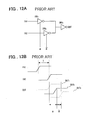
- Fig. 12A is a diagram illustrating an example of the interpolator structure
- Fig. 12B is a diagram useful in describing the operating principle of the interpolator, namely internal division of phase difference.
- the interpolator having the structure of Fig. 12A is such that output timing varies in proportion to the driving capability of juxtaposed inverters.
- N represent the number of inverters INV1 rendered active or inactive by a control signal ⁇ (N is 16 in the case of a 16-step interpolator), and let N represent the number of inverters INV2 rendered active or inactive by an inverted control signal ⁇ - obtained by inverting the control signal ⁇ .
- Each of the parallel-connected inverters INV1 is represented by a single inverter and each of the parallel-connected inverters INV2 is represented by a single inverter in Fig. 12A.
- the inverter INV1 is such that a switch (not shown) inserted between a CMOS inverter constituting the inverter INV1 and a power-supply bus is turned on when the control signal ⁇ is at the high level
- the inverter INV2 is such that a switch (not shown) inserted between a CMOS inverter constituting the inverter INV2 and a power-supply bus is turned on when the control signal ⁇ - is at the high level.
- the output terminals of the inverters INV1, INV2 are tied together and connected to the input terminal of an inverter INV3.
- C represent the capacitance at the connection node of the output terminals of the inverters INV1, INV2 N-number of each of which are provided in parallel.
- CV represent the amount of electric charge to be discharged from the connection node (capacitance C) until the output OUT of the inverter INV3 inverts, and let I represent the discharge current of the inverters INV1, INV2.
- n-number (0 ⁇ n ⁇ N) of the control signals ⁇ are placed at the high level and, hence, (N-n)-number of the inverted control signals ⁇ - are placed at the high level, then n-number of the inverters INV1 and (N-n)-number of the inverters INV2 will be activated.
- the n-number of inverters INV1 discharge the accumulated charge in the capacitance C at a current n I I for a time T at the rising edge of input signal IN1, whereby the electric charge in the capacitance becomes CV - n ⁇ IT, where T represents the time difference (phase difference) between the rising edges of input signals IN1 and IN2.
- n-number of the inverters INV1 and (N-n)-number of inverters INV2 discharge the accumulated charge of the capacitance C at a discharge current N ⁇ I at the rising edge of the input signal IN2 following elapse of the time T from the rising edge of input signal IN1.
- the propagation delay time tpd is minimized and is given by CV/N ⁇ I (see OUT1 in Fig. 12B).
- the propagation delay time tpd is maximized and is given by T + CV/N ⁇ I (see OUT3 in Fig. 12B).
- the control signal supplied from the decoder 106 is applied commonly to the plurality of interpolators 111 in the phase-shift circuit 101A, and all of the multiphase clock signals are shifted in unison at regular intervals at a prescribed phase in dependence upon the control signal.
- phase of the clock situated in the data changeover portion is shifted in a case where the timing of the data transition point shifts owing to jitter, etc., of the input data
- the phase of the clock of another phase for sampling the value of the data bit also is shifted by the same amount.
- data of the correct value will no longer be able to be sampled.
- the phase of the data transition point is delayed in a certain cycle owing to jitter of the input data or the like in a case where the data transition and the content of the data bit are being sampled by two phases, then there will also be a case where the phase of the data transition point is advanced in the next cycle (i.e., one cycle is shortened).
- an object of the present invention is to provide a clock and data recovery circuit and method that make it possible to suppress the effects of jitter components and to sample data accurately.
- a clock and data recovery circuit comprising: a phase-shift circuit having a switch, to which a plurality of clocks (referred to as a "multiphase clocks") of mutually different phases are input, for selecting and outputting a plurality of pairs of clocks from among the multiphase clocks, and a plurality of interpolators, to which the plurality of clock pairs output from the switch are input, for outputting signals in which delay time is stipulated by time obtained by internally dividing the phase difference between the clocks of the pair applied thereto; a plurality of latch circuits to which input data is applied in common, the plurality of latch circuits sampling and outputting the input data at transition edges of clocks of mutually shifted phases supplied from the interpolators corresponding to respective ones of the plurality of latch circuits; a phase detecting circuit for detecting and outputting phase, with respect to the clock, of a transition point of the input data from the outputs of the plurality of latch circuits; a filter for smooth
- the foregoing object is attained by providing a clock control method of a clock and data recovery circuit having a plurality of latch circuits to which input data is applied in common, the plurality of latch circuits sampling and outputting the input data at transition edges of clocks of mutually shifted phases supplied to respective ones of the plurality of latch circuits; a phase detecting circuit for detecting and outputting phase, with respect to the clock, of a transition point of the input data from the outputs of the plurality of latch circuits; a filter for smoothing the output of the phase detecting circuit; and a control circuit for controlling the clock phase based upon the output of the filter; a plurality of pairs of clocks being selected and output from among a plurality of clocks (referred to as a "multiphase clocks") of mutually different phases by a switch to which the multiphase clocks are input, and signals in which delay time is stipulated by time obtained by internally dividing the phase difference between the clocks of the pair being output by a plurality of interpolators
- a clock and data recovery circuit according to a preferred mode of practicing the present invention comprises: a phase-shift circuit 101 having a switch 110, to which a plurality of clocks of mutually different phases are input, for selecting and outputting a plurality of pairs of clocks from among the plurality of clocks, and a plurality of interpolators 111 (e.g., Int. 1 to Int. 8 in Fig.
- a plurality of latch circuits 102 e.g., flip-flops F/F1 to F/F8 for sampling input data at rising or falling edges of the clocks (CLK1 to CLK8) output from respective ones of the interpolators 111; a counter 103 for counting up/down a count value in which outputs of the plurality of latch circuits 102 (F/F1 to F/F8) indicate counting up or counting down; a filter 105 for averaging the output of the counter over time; and a control circuit 107 for decoding output of the filter 105 and outputting a control signal U for controlling changeover of the switch 110 in the phase-shift circuit 101 and a control signal S for setting the division ratios of the interpolators 111.
- the control circuit 107 outputs control signals Seven, Sodd for
- the interpolators 111 comprise a first group of N-number of inverters (INV1 in Fig. 12A) to which a first input signal from a first input terminal is input as a common signal and which are activated and deactivated by a first control signal supplied from the control circuit 107, and a second group of N-number of inverters (INV2 in Fig. 12A) to which a second input signal from a second input terminal is input as a common signal and which are activated and deactivated by a second control signal, which is the inverted signal of the first control signal supplied from the control circuit 107.
- the outputs of the inverters of the first group and the outputs of the inverters of the second group are tied together and connected to the input terminal of a third inverter (INV3 in Fig. 12A).
- n (0 ⁇ n ⁇ N) represent the number of inverters of the first group that are activated by the first control signal.
- the third inverter outputs a signal having a delay time stipulated by a time obtained by internally dividing time T, which corresponds to the phase difference between the first and second input signals, at a ratio (N-n):n.
- the phase of the output signal is set in variable fashion.
- the counter 103 which constitutes a phase detecting circuit, is counted up and down based upon the outputs of the plurality of latch circuits (F/F1 to F/F8) 102, and the filter 105 comprises a digital filter (averaging filter).
- the combination of pairs of clocks in the switch 110 is changed over based upon changeover signal U that is output from the control circuit 107, the division ratios of the odd- and even-numbered interpolators 111 are variably set separately based upon the control signals Sodd, Seven, respectively, that are output from the control circuit 107, and the phases of the clocks output from the odd- and even-numbered interpolators 111 are controlled separately.
- the control circuit 107 exercises control for advancing or delaying phase, depending upon jitter of the input data DATA, of the clock signal that samples the data changeover point, the phase of the clock for sampling the data bit remains as before without being immediately changed in association with the change in the phase of the clock signal that samples the data changeover point.
- such control makes it possible to avoid erroneous sampling of data.
- sets each composed of output data, which is delivered from the plurality of latch circuits (flip-flops F/F1 to F/F8), and a clock (e.g., a clock of one phase) output from the phase-shift circuit 101 are input to a selector (selection circuit) 104, which selects and outputs any set.
- a selector selection circuit
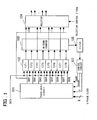
- Fig. 1 is a diagram illustrating the structure of a preferred embodiment of the invention.
- this embodiment of the clock and data recovery circuit comprises phase-shift circuit 101, to which an 8-phase clock is input, for outputting an 8-phase clock that has undergone a phase shift; the plurality of D-type flip-flops 102 (F/F1 to F/F8), to the data input terminals of which the clocks output from the phase-shift circuit 101 are input, and to the data input terminals of which the input data DATA is input, for sampling the input data DATA at the rising edges of the clocks; counter 103 the count of which is counted up or down by an up signal or down signal, wherein outputs of the plurality of D-type flip-flops 102 serve as up signals when they are, e.g., logical "1" and down signals when they are logical "0"; filter 105 for averaging the output of
- the outputs of flip-flops F/F1, F/F3, F/F5, F/F7 from among the plurality of D-type flip-flops 102 are input to the selector 104.
- an arrangement in which the outputs of all of the flip-flops F/F1 to F/F8 are input to the selector 104 may be adopted.
- the plurality of D-type flip-flops 102 sample and output the input data DATA at the rising edges (or falling edges) of the clocks CLK1 to CLK8 that are output from the phase-shift circuit 101.
- the counter 103 counts the outputs of the plurality of D-type flip-flops 102, and the count is smoothed at a predetermined time constant by the filter 105. On the basis of this smoothed signal, control to advance or delay the phases of the clocks supplied to the plurality of D-type flip-flops 102 is carried out. Thus, clock and data locked to the input data DATA are output.
- Fig. 2 is a diagram illustrating the structure of the phase-shift circuit 101 according to this embodiment of the present invention.
- the phase-shift circuit 101 includes the switch 110 to which the 8-phase clock (8-phase CLK) is input, and the eight interpolators 111 (Int. 1 to Int. 8) to each of which a clock pair output from the switch 110 is input.
- the switch 110 comprises, e.g., a rotary switch and changes over the combination of output clock pairs based upon the output signal U from the control circuit 107.
- the control circuit 107 outputs the control signal Sodd to the odd-numbered interpolators 111 (Int. 1, Int. 3, Int. 5, Int. 7) and outputs the control signal Seven to the even-numbered interpolators 111 (Int. 2, Int. 4, Int. 6, Int. 8).
- Fig. 3 is a diagram illustrating the structure of the switch 110 (rotary switch) and interpolator 111 depicted in Fig. 2.
- the control circuit 107 includes a decoder (not shown) for outputting the control signal (changeover signal) U that controls changeover of the switch 110 and the control signal S that controls the division ratio of the first group of interpolators, and a comparator circuit (or hysteresis circuit) for outputting a control signal S' for controlling the division ratio of the second group of interpolators.
- the decoder (not shown) in the control circuit 107 has a structure identical with that of the decoder 106 shown in Figs. 9, 10, decodes the output of the filter 105 and outputs the switch changeover signal U and control signal S for setting the division ratio of odd-numbered interpolators 111 1 , 111 3 , 111 5 , 111 7 .
- the signal U of the four higher order bits is used to control changeover of the switch 110
- the signal S of the four lower order bits is used to control the 16-step interpolators 111 1 , 111 3 , 111 5 , 111 7 .
- the 16-step control signal (four bits) supplied to these interpolators undergoes a thermometer-type shift. In a case where it is necessary to delay or advance phase with the 16-step control signal being all "1"s or all "0"s, the clock pairs are changed over in the switch 110 by the changeover signal U.
- the comparator circuit (or hysteresis circuit) within the control circuit 107 outputs the control signal S' for setting the division ratio of the even-numbers interpolators 111 2 , 111 4 , 111 6 , 111 8 .
- the 16-step control signal S' supplied to these interpolators undergoes a thermometer-type shift.
- control signal S and the signal obtained by inverting the control signal S by the inverter INV1 are supplied to the odd-numbered interpolators, and the control signal S' and the signal obtained by inverting the control signal S' by the inverter INV2 are supplied to the even-numbered interpolators.
- control circuit 107 In a case where the control circuit 107 is such that identical bits of the plurality of bits constituting the control signal S' continue a plurality of times, thereby specifying advance/delay of the phases of the corresponding interpolators, the control circuit 107 performs control to advance/delay the phases of the corresponding interpolators incrementally.
- the rotary switch includes a first switch 110-1, to which odd-numbered phase clocks (P0, P2, P4, P6) of the eight phase clocks P0 to P7 are input, for selecting and outputting these to each of the interpolators 111, and a second switch 110-2, to which even-numbered phase clocks (P1, P3, P5, P7) of the multiphase clocks P0 to Pn are input, for selecting and outputting these to each of the interpolators 111.
- the initial state a state in which changeover.
- clock pairs (P0,P1), (P1,P2), (P2,P3), (P3,P4), (P4,P5), (P5,P6), (P6,P7), (P7,P0), which are output from the first switch 110-1 and second switch 110-2, are input to the interpolators 111 1 to 111 8 , respectively, by way of example.
- the changeover signal U for changing over the combinations of clock pairs supplied to the interpolators 111 1 to 111 8 is output to the switches 110-1, 110-2.
- the switch 110 is referred to as a rotary switch because it rotates the clock-pair combinations.
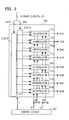
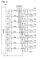
- Fig. 4 is a diagram illustrating an example of the structure of the control circuit 107 according to the embodiment of the invention shown in Figs. 1 and 2.
- the arrangement of Fig. 4 includes the decoder 106, which is identical with the decoder shown in Figs. 9 and 10.
- the decoder 106 outputs control signals S0 to S7 of eight bits.
- the interpolators whose division ratio is varied by these control signals of eight bits are 256-step interpolators.
- the control signals of eight bits output from the decoder 106 in the control circuit 107 are latched by latch circuits 120 1 to 120 8 comprising D-type flip-flops and are extracted as control signals SO to S7 for controlling the division ratios of the odd-numbered interpolators.
- the outputs of the latch circuits 120 1 to 120 8 are latched by latch circuits 121 1 to 121 8 , respectively, comprising D-type flip-flops.
- the control circuit 107 further includes 2-input, 1-output logic gates 122 1 to 122 8 to which the outputs of the latch circuits 120 1 to 120 8 , respectively, and the outputs of the latch circuits 121 1 to 121 8 , respectively, are input.
- control signals S0' to S7' for controlling the division ratios of the even-numbered interpolators.
- control signals S0 to S7 and signals obtained by inverting the control signals S0 to S7 are supplied to the odd-numbered interpolators, and signals obtained by inverting the control signals S0' to S7' are supplied to the even-numbered interpolators.
- the logic gates 122 1 to 122 8 comprise AND gates that output the high level when, e.g., two signals input to each of the logic gates 122 1 to 122 8 are both at the high level (when the value latched previously and the currently latched value are both logical "1").
- an arrangement having hysteresis may be adopted, wherein logical "1" is output when the previously latched value is logical "0" and the currently latched value is logical "1".
- the circuit groups 121, 122 construct a group of comparator circuits (group of hysteresis circuits).
- Fig. 4 The arrangement of Fig. 4 is such that the value of the applicable bit of the corresponding control signal S' is set based upon two items of time-series data with regard to each bit of the control signals S0 to S7 in circuits 121, 122.
- an alternative arrangement may be adopted in which if three or more items of time-series data are monitored with regard to each bit of the control signals S0 to S7 and agreement is achieved with a desired pattern, then the applicable bit of the control signal S' is changed.
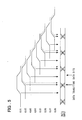
- Fig. 5 is a timing diagram useful in describing the operation of this embodiment of the invention.
- Fig. 5 illustrates clocks CLK1 to CLK8 of eight phases output from the phase-shift circuit 101 and the waveform of the data input.
- clocks CLK1, CLK3, CLK5, CLK7 sample (latch the data) the data bits
- clocks CLK2, CLK4, CLK6, CLK8 sample (i.e., perform edge detection) the changeover portions (transition points) of the input data in a case where the data changeover point and data bit are sampled in two phases [see Equation (1) above]. It will be understood that even in a case where the phases of clocks for sampling the data changeover portion are shifted as indicated by the broken lines in the timing diagram of Fig. 5, the phases of the clocks for sampling the data bit do not change and the value of the data bit is sampled correctly.
- Figs. 6A, 6B and 6C are diagrams useful in describing the operation of this embodiment.
- Fig. 6A illustrates the data input, in which reference characters tA, tB, ⁇ tG represent sampling points (times) based upon the multiphase clock.
- Fig. 6B illustrates an example of the control signals S0 to S7 and control signals S0' to S7' that are output from the control circuit 107 in correspondence with the sampling points tA, tB, ⁇ tG.
- control signals S0 to S7 for controlling the phases of the interpolators that output the sampling clocks for detecting the data transition point the value of S3 changes from moment to moment in the manner of logical "0", logical "1" owing to the effect of jitter or the like.
- control for advancing or retarding phase is carried out depending upon jitter or the like in the input data in the interpolators that supply the sampling clock for detecting the data transition point.
- S0' to S7' do not change and the phases remain as they were originally.
- Fig. 7 is a diagram illustrating a specific example of the structure of the interpolator 111 at the transistor level.
- the interpolator includes a P-channel MOS transistor MP51, which is connected between a power source VDD and an internal node N51, turned on when the output signal of an OR gate 51, the inputs to which are IN1 and IN2, assumes the low level.
- a plurality of series circuits (MN51 and C1, ⁇ , MN58 and C8), each of which comprises an N-channel MOS transistor and a capacitor, are connected in parallel between the internal node N51 and ground.
- the interpolator further includes an inverter INV51, which has the internal node N51 connected to its input, for extracting an output signal OUT delivered from its output terminal.
- a control signal Cnt (0:7) connected to the gates of N-channel MOS transistors MN51 to MN58 may be set by the output of a frequency sensing circuit (not shown) for sensing the frequency of the clock signal.
- the control signal Cnt (0:7) may be decided by setting registers or dip switches, etc., to desired values in accordance with the particular application.
- the capacitance value applied to the node N51 can be varied by the control signal Cnt (0:7), thereby making it possible to widen the frequency range that can be supported.
- the interpolator further includes 2N-number of parallel-connected N-channel MOS transistors MN11 to MN1N, MN21 to MN2N whose drains are connected to the internal node N51, and 2N-number of N-channel MOS transistors MN31 to MN3N, MN41 to MN4N whose drains are connected to the sources of the 2N-number of N-channel MOS transistors MN11 to MN1N, MN21 to MN2N, respectively, and whose sources are connected to ground.
- the input signal IN1 is connected as a common signal to the gates of N-number of the N-channel MOS transistors MN11 to MN1N, which are half of the above-mentioned 2N-number of N-channel MOS transistors, and the input signal IN2 is connected as a common signal to the gates of the N-number of N-channel MOS transistors MN21 to MN2N, which are other half of the above-mentioned 2N-number of N-channel MOS transistors.
- a prescribed number of the N-channel MOS transistors MN31 to MN3N and of the N-channel MOS transistors MN41 to MN4N are turned on by control signals (N-bit control code) S[0] to S[N-1] and control signals (N-bit control code) SB[0] to SB[N-1] input to the gates of the N-channel MOS transistors MN31 to MN3N, MN41 to MN4N.
- the N-bit control signals S[0:N-1], SB[0:N-1] are input from the decoder 106, and signals SB[0] to SB[N-1] are applied as complementary signals obtained by inverting S[0] to S[N-1] by an inverter (inverter INV in Fig. 3).
- the P-channel MOS transistor MP51 When the input signals IN1, IN2 are at the low level, the P-channel MOS transistor MP51, to the gate of which the output of OR gate 51 is input, turns on, thereby charging capacitor C by the current from the power supply.
- the capacitance value is the combined capacitance value of capacitors among capacitors C1 to C8 connected to the N-channel MOS transistors MN51 to MN58 turned on by the control signal Cnt.
- the N-channel MOS transistors MN11 to MN1N are turned on and the charge that has accumulated in the capacitor C is partially discharged via a path composed of n-number of N-channel MOS transistors turned on by the control signals S[0] to S[N-1] from among the N-channel MOS transistors MN31 to MN3N having drains connected to the sources of the N-channel MOS transistors MN11 to MN1N and sources are connected to ground, and to the gates of which the control signals S[0] to S[N-1] are input.
- the N-channel MOS transistors MN21 to MN2N are turned on and the charge that has accumulated in the capacitor C is partially discharged via a path composed of (N-n)-number of N-channel MOS transistors turned on by the control signals SB[0] to SB[N-1] from among the N-channel MOS transistors MN41 to MN4N having drains connected to the sources of the N-channel MOS transistors MN21 to MN2N and sources are connected to ground and to the gates of which the control signals S[0] to S[N-1] are input.
- CV represent the electric charge that is discharged until the output of the inverter INV51, to which the terminal voltage of capacitor C is input, is inverted to the high level.
- the charge is discharged at a current nI for the time of the phase difference (T) following the transition of the input signal IN1 to the high level.
- T phase difference
- the input signal IN1 undergoes a transition to the high level and the charge is discharged at a drain current NI of a total of N-number of N-channel MOS transistors, namely n-number of N-channel MOS transistors MN11 to MN1n and (N-n)-number of N-channel MOS transistors MN21 to MN2(N-n).
- the delay time tpd from the positive-going transition of the input signal IN2 from the low to the high level to the positive going transition of the output OUT is represented by the following equation: and delay time can be varied in steps of T/N, where T is the phase difference between the inputs IN1 and IN2.
- the positions of transistors MN11 to MN1N and transistors MN31 to MN3N and the positions of transistors MN21 to MN2N and transistors MN41 to MN4N may be interchanged. That is, it is of course permissible to adopt an arrangement in which the drains of the transistors MN31 to MN3N, to the gates of which the control signals S[0] to S[N-1], respectively, are input, are connected to the internal node N51; the transistors MN11 to MN1N, to the gates of which the input signal IN1 is input as a common signal, are connected between the sources of the transistors MN31 to MN3N and ground; the drains of the transistors MN41 to MN4N, to the gates of which the control signals SB[0] to SB[N-1], respectively, are input, are connected to the internal node N51; and the transistors MN21 to MN2N, to the gates of which the input signal IN2 is input as a common signal, are
- the multiphase clock may be produced by the VCO of a PLL. In such case the clock is extracted from an inverter circuit of a prescribed stage of the VCO ring oscillator.
- the multiphase clock may be produced by a frequency multiplier of the multiphase clock.
- the multiphase clock supplied to the phase-shift circuit 101 is generated using a multiphase clock generating circuit employing a frequency multiplying interpolator (multiphase-clock frequency dividing circuit) described in the specification of Japanese Patent Application No. 2000-389526 (Japanese Patent Kokai Publication JP-A-P2002-190724A).
Landscapes
- Engineering & Computer Science (AREA)
- Computer Networks & Wireless Communication (AREA)
- Signal Processing (AREA)
- Physics & Mathematics (AREA)
- Nonlinear Science (AREA)
- Stabilization Of Oscillater, Synchronisation, Frequency Synthesizers (AREA)
- Synchronisation In Digital Transmission Systems (AREA)
- Pulse Circuits (AREA)
- Manipulation Of Pulses (AREA)
Applications Claiming Priority (2)
| Application Number | Priority Date | Filing Date | Title |
|---|---|---|---|
| JP2002142535A JP3802447B2 (ja) | 2002-05-17 | 2002-05-17 | クロックアンドデータリカバリ回路とそのクロック制御方法 |
| JP2002142535 | 2002-05-17 |
Publications (3)
| Publication Number | Publication Date |
|---|---|
| EP1363399A2 true EP1363399A2 (de) | 2003-11-19 |
| EP1363399A3 EP1363399A3 (de) | 2010-03-31 |
| EP1363399B1 EP1363399B1 (de) | 2011-03-23 |
Family
ID=29267830
Family Applications (1)
| Application Number | Title | Priority Date | Filing Date |
|---|---|---|---|
| EP03010522A Expired - Lifetime EP1363399B1 (de) | 2002-05-17 | 2003-05-09 | Schaltungsanordnung zur Daten- und Taktrückgewinnung und entsprechendes Taktkontrollverfahren |
Country Status (4)
| Country | Link |
|---|---|
| US (1) | US6753712B2 (de) |
| EP (1) | EP1363399B1 (de) |
| JP (1) | JP3802447B2 (de) |
| DE (1) | DE60336437D1 (de) |
Cited By (3)
| Publication number | Priority date | Publication date | Assignee | Title |
|---|---|---|---|---|
| WO2007078700A1 (en) * | 2005-12-28 | 2007-07-12 | Intel Corporation | Receive clock deskewing method, apparatus and system |
| EP1898548A1 (de) * | 2006-09-05 | 2008-03-12 | Ricoh Company, Ltd. | Überabtastungsschaltung und Überabtastungsverfahren |
| EP2079210A4 (de) * | 2006-10-11 | 2011-06-29 | Thine Electronics Inc | Taktdatenwiedergewinnungseinrichtung |
Families Citing this family (49)
| Publication number | Priority date | Publication date | Assignee | Title |
|---|---|---|---|---|
| JP3636657B2 (ja) * | 2000-12-21 | 2005-04-06 | Necエレクトロニクス株式会社 | クロックアンドデータリカバリ回路とそのクロック制御方法 |
| US6977539B1 (en) * | 2003-08-26 | 2005-12-20 | Integrated Device Technology, Inc. | Clock signal generators having programmable full-period clock skew control and methods of generating clock signals having programmable skews |
| US7151398B2 (en) * | 2003-08-26 | 2006-12-19 | Integrated Device Technology, Inc. | Clock signal generators having programmable full-period clock skew control |
| US7323917B2 (en) * | 2003-09-15 | 2008-01-29 | Texas Instruments Incorporated | Method and apparatus for synthesizing a clock signal having a frequency near the frequency of a source clock signal |
| US7668271B2 (en) * | 2003-09-30 | 2010-02-23 | Rambus Inc. | Clock-data recovery (“CDR”) circuit, apparatus and method for variable frequency data |
| JP4480536B2 (ja) * | 2003-12-05 | 2010-06-16 | 株式会社リコー | データリカバリ方法およびデータリカバリ回路 |
| JP4376611B2 (ja) * | 2003-12-19 | 2009-12-02 | パナソニック株式会社 | 周波数変調回路 |
| JP2005223829A (ja) | 2004-02-09 | 2005-08-18 | Nec Electronics Corp | 分数分周回路及びこれを用いたデータ伝送装置 |
| US7428282B2 (en) * | 2004-04-15 | 2008-09-23 | Texas Instruments Incorporated | Timing recovery of PAM signals using baud rate interpolation |
| TW200620938A (en) | 2004-09-07 | 2006-06-16 | Nec Electronics Corp | Synchronization device and semiconductor device |
| US7583459B1 (en) * | 2004-11-18 | 2009-09-01 | Marvell International Ltd. | Method and apparatus for write precompensation in a magnetic recording system |
| US7209008B2 (en) * | 2005-04-25 | 2007-04-24 | Fortemedia Inc. | Multiple output phase-locked loop (PLL) using a single voltage controlled oscillator (VCO) |
| JP2007036869A (ja) * | 2005-07-28 | 2007-02-08 | Nec Electronics Corp | シリアルパラレル変換、パラレルシリアル変換、fifo一体回路 |
| US7599457B2 (en) * | 2005-08-08 | 2009-10-06 | Lattice Semiconductor Corporation | Clock-and-data-recovery system having a multi-phase clock generator for one or more channel circuits |
| JP4756954B2 (ja) | 2005-08-29 | 2011-08-24 | ルネサスエレクトロニクス株式会社 | クロックアンドデータリカバリ回路 |
| JP4668750B2 (ja) * | 2005-09-16 | 2011-04-13 | 富士通株式会社 | データ再生回路 |
| US8090065B2 (en) * | 2005-11-29 | 2012-01-03 | Sonosite, Inc. | Implied clock |
| JP4749168B2 (ja) * | 2006-02-01 | 2011-08-17 | ルネサスエレクトロニクス株式会社 | クロックアンドデータリカバリ回路 |
| US20080186618A1 (en) * | 2007-02-05 | 2008-08-07 | Broadcom Corporation, A California Corporation | Architecture for write pre-compensation |
| US7673274B2 (en) * | 2007-04-19 | 2010-03-02 | L3 Communications Integrated Systems, LP | Datapipe interpolation device |
| US8223909B2 (en) * | 2007-06-15 | 2012-07-17 | Panasonic Corporation | Digital sampling apparatuses and methods |
| US7515073B2 (en) * | 2007-08-17 | 2009-04-07 | Infineon Technologies Ag | Digital sample rate conversion |
| CN101388665B (zh) * | 2007-09-14 | 2011-11-09 | 瑞昱半导体股份有限公司 | 时间交错式时脉数据恢复装置及方法 |
| JP2010147558A (ja) | 2008-12-16 | 2010-07-01 | Renesas Electronics Corp | クロックデータリカバリ回路 |
| JP2011055048A (ja) * | 2009-08-31 | 2011-03-17 | Renesas Electronics Corp | 多相クロック生成回路 |
| JP5259563B2 (ja) * | 2009-12-22 | 2013-08-07 | 株式会社東芝 | 情報処理装置およびその制御方法 |
| US9041452B2 (en) * | 2010-01-27 | 2015-05-26 | Silicon Laboratories Inc. | Circuit and method of clocking multiple digital circuits in multiple phases |
| US8139701B2 (en) * | 2010-08-05 | 2012-03-20 | Fujitsu Limited | Phase interpolation-based clock and data recovery for differential quadrature phase shift keying |
| JP5330340B2 (ja) | 2010-08-31 | 2013-10-30 | 株式会社東芝 | サンプリング位相を補正するホストコントローラ及び方法 |
| TWI420450B (zh) * | 2010-12-23 | 2013-12-21 | Au Optronics Corp | 移位暫存器的時脈訊號供應方法與電路 |
| JP5724394B2 (ja) * | 2011-01-11 | 2015-05-27 | 富士通株式会社 | 受信回路、伝送システムおよび受信方法 |
| US8451969B2 (en) * | 2011-03-15 | 2013-05-28 | Intel Corporation | Apparatus, system, and method for timing recovery |
| US9109888B2 (en) * | 2012-03-21 | 2015-08-18 | Honda Motor Co., Ltd. | Distance measuring system |
| US8923375B2 (en) * | 2012-06-29 | 2014-12-30 | Parade Technologies, Inc. | On die jitter tolerance test |
| TWI487269B (zh) * | 2012-07-23 | 2015-06-01 | Mstar Semiconductor Inc | 相位內插裝置以及相位內插方法 |
| US9281749B2 (en) * | 2012-08-13 | 2016-03-08 | Northrop Grumman Systems Corporation | Multiple power supply systems and methods |
| JP6136711B2 (ja) * | 2013-07-29 | 2017-05-31 | 富士通株式会社 | 受信回路 |
| US9112655B1 (en) * | 2013-07-30 | 2015-08-18 | Altera Corporation | Clock data recovery circuitry with programmable clock phase selection |
| US9350527B1 (en) * | 2015-03-24 | 2016-05-24 | Sony Corporation | Reception unit and receiving method |
| KR20160145217A (ko) * | 2015-06-09 | 2016-12-20 | 에스케이하이닉스 주식회사 | 카운팅 회로, 그 카운팅 회로를 포함하는 이미지 센싱 장치 및 그 이미지 센싱 장치의 리드아웃 방법 |
| JP6592986B2 (ja) * | 2015-06-26 | 2019-10-23 | 株式会社ソシオネクスト | Cdr制御回路、cdr回路およびcdr制御方法 |
| JP6819219B2 (ja) | 2016-10-28 | 2021-01-27 | 富士通株式会社 | クロック再生回路,半導体集積回路装置およびrfタグ |
| CN110719088B (zh) * | 2018-07-13 | 2023-04-07 | 瑞昱半导体股份有限公司 | 时钟产生电路与混合式电路 |
| KR102509984B1 (ko) * | 2018-10-12 | 2023-03-14 | 삼성전자주식회사 | 클락 신호의 주파수 및 위상을 감지하는 집적 회로 및 이를 포함하는 클락 및 데이터 복원 회로 |
| US11283436B2 (en) * | 2019-04-25 | 2022-03-22 | Teradyne, Inc. | Parallel path delay line |
| US10756711B1 (en) * | 2019-11-13 | 2020-08-25 | Xilinx, Inc. | Integrated circuit skew determination |
| CN115985356B (zh) * | 2021-10-15 | 2024-09-13 | 长鑫存储技术有限公司 | 数据合成器 |
| US11711200B2 (en) | 2021-12-16 | 2023-07-25 | Analog Devices, Inc. | Multiphase clock generators with digital calibration |
| US12200090B1 (en) * | 2022-02-25 | 2025-01-14 | Acacia Communications, Inc. | Multiphase clock generation with automatic skew and amplitude control |
Family Cites Families (5)
| Publication number | Priority date | Publication date | Assignee | Title |
|---|---|---|---|---|
| US6122336A (en) * | 1997-09-11 | 2000-09-19 | Lsi Logic Corporation | Digital clock recovery circuit with phase interpolation |
| US6285726B1 (en) * | 1998-05-18 | 2001-09-04 | National Semiconductor Corporation | 10/100 mb clock recovery architecture for switches, repeaters and multi-physical layer ports |
| JP3789247B2 (ja) * | 1999-02-26 | 2006-06-21 | Necエレクトロニクス株式会社 | クロック周期検知回路 |
| JP3495311B2 (ja) * | 2000-03-24 | 2004-02-09 | Necエレクトロニクス株式会社 | クロック制御回路 |
| JP3636657B2 (ja) | 2000-12-21 | 2005-04-06 | Necエレクトロニクス株式会社 | クロックアンドデータリカバリ回路とそのクロック制御方法 |
-
2002
- 2002-05-17 JP JP2002142535A patent/JP3802447B2/ja not_active Expired - Fee Related
-
2003
- 2003-05-02 US US10/427,928 patent/US6753712B2/en not_active Expired - Fee Related
- 2003-05-09 DE DE60336437T patent/DE60336437D1/de not_active Expired - Lifetime
- 2003-05-09 EP EP03010522A patent/EP1363399B1/de not_active Expired - Lifetime
Cited By (7)
| Publication number | Priority date | Publication date | Assignee | Title |
|---|---|---|---|---|
| WO2007078700A1 (en) * | 2005-12-28 | 2007-07-12 | Intel Corporation | Receive clock deskewing method, apparatus and system |
| GB2447362A (en) * | 2005-12-28 | 2008-09-10 | Intel Corp | Receive clock deskewing method,apparatus and system |
| US7439788B2 (en) | 2005-12-28 | 2008-10-21 | Intel Corporation | Receive clock deskewing method, apparatus, and system |
| GB2447362B (en) * | 2005-12-28 | 2010-09-01 | Intel Corp | Receive clock deskewing method,apparatus,and system |
| EP1898548A1 (de) * | 2006-09-05 | 2008-03-12 | Ricoh Company, Ltd. | Überabtastungsschaltung und Überabtastungsverfahren |
| EP2079210A4 (de) * | 2006-10-11 | 2011-06-29 | Thine Electronics Inc | Taktdatenwiedergewinnungseinrichtung |
| US8045664B2 (en) | 2006-10-11 | 2011-10-25 | Thine Electronics, Inc. | Clock data recovery device |
Also Published As
| Publication number | Publication date |
|---|---|
| DE60336437D1 (de) | 2011-05-05 |
| JP2003333021A (ja) | 2003-11-21 |
| US6753712B2 (en) | 2004-06-22 |
| US20030214335A1 (en) | 2003-11-20 |
| EP1363399A3 (de) | 2010-03-31 |
| EP1363399B1 (de) | 2011-03-23 |
| JP3802447B2 (ja) | 2006-07-26 |
Similar Documents
| Publication | Publication Date | Title |
|---|---|---|
| EP1363399B1 (de) | Schaltungsanordnung zur Daten- und Taktrückgewinnung und entsprechendes Taktkontrollverfahren | |
| JP3636657B2 (ja) | クロックアンドデータリカバリ回路とそのクロック制御方法 | |
| KR100399209B1 (ko) | 클럭 제어 회로 및 클럭 제어 방법 | |
| US6583655B2 (en) | Clock control circuit | |
| KR100436604B1 (ko) | 클럭 제어회로 및 클럭 제어방법 | |
| US6642760B1 (en) | Apparatus and method for a digital delay locked loop | |
| US6693985B2 (en) | Clock and data recovery method and apparatus | |
| EP1189348B1 (de) | Verfahren und Schaltung zur Taktsteuerung | |
| US7327176B2 (en) | Delay circuit and delay synchronization loop device | |
| US7912167B2 (en) | Clock and data recovery circuit | |
| US6742133B2 (en) | Clock controlling method and clock control circuit | |
| US8502586B1 (en) | Methods of clock signal generation with selected phase delay | |
| US7750711B2 (en) | Phase select circuit with reduced hysteresis effect |
Legal Events
| Date | Code | Title | Description |
|---|---|---|---|
| PUAI | Public reference made under article 153(3) epc to a published international application that has entered the european phase |
Free format text: ORIGINAL CODE: 0009012 |
|
| AK | Designated contracting states |
Kind code of ref document: A2 Designated state(s): AT BE BG CH CY CZ DE DK EE ES FI FR GB GR HU IE IT LI LU MC NL PT RO SE SI SK TR |
|
| AX | Request for extension of the european patent |
Extension state: AL LT LV MK |
|
| PUAL | Search report despatched |
Free format text: ORIGINAL CODE: 0009013 |
|
| AK | Designated contracting states |
Kind code of ref document: A3 Designated state(s): AT BE BG CH CY CZ DE DK EE ES FI FR GB GR HU IE IT LI LU MC NL PT RO SE SI SK TR |
|
| AX | Request for extension of the european patent |
Extension state: AL LT LV MK |
|
| GRAP | Despatch of communication of intention to grant a patent |
Free format text: ORIGINAL CODE: EPIDOSNIGR1 |
|
| 17P | Request for examination filed |
Effective date: 20100701 |
|
| RIC1 | Information provided on ipc code assigned before grant |
Ipc: H03K 5/00 20060101AFI20100729BHEP |
|
| RAP1 | Party data changed (applicant data changed or rights of an application transferred) |
Owner name: RENESAS ELECTRONICS CORPORATION |
|
| AKX | Designation fees paid |
Designated state(s): DE GB |
|
| GRAS | Grant fee paid |
Free format text: ORIGINAL CODE: EPIDOSNIGR3 |
|
| GRAA | (expected) grant |
Free format text: ORIGINAL CODE: 0009210 |
|
| AK | Designated contracting states |
Kind code of ref document: B1 Designated state(s): DE GB |
|
| REG | Reference to a national code |
Ref country code: GB Ref legal event code: FG4D |
|
| REF | Corresponds to: |
Ref document number: 60336437 Country of ref document: DE Date of ref document: 20110505 Kind code of ref document: P |
|
| REG | Reference to a national code |
Ref country code: DE Ref legal event code: R096 Ref document number: 60336437 Country of ref document: DE Effective date: 20110505 |
|
| PLBE | No opposition filed within time limit |
Free format text: ORIGINAL CODE: 0009261 |
|
| STAA | Information on the status of an ep patent application or granted ep patent |
Free format text: STATUS: NO OPPOSITION FILED WITHIN TIME LIMIT |
|
| 26N | No opposition filed |
Effective date: 20111227 |
|
| REG | Reference to a national code |
Ref country code: DE Ref legal event code: R097 Ref document number: 60336437 Country of ref document: DE Effective date: 20111227 |
|
| PGFP | Annual fee paid to national office [announced via postgrant information from national office to epo] |
Ref country code: DE Payment date: 20130515 Year of fee payment: 11 Ref country code: GB Payment date: 20130508 Year of fee payment: 11 |
|
| REG | Reference to a national code |
Ref country code: DE Ref legal event code: R119 Ref document number: 60336437 Country of ref document: DE |
|
| GBPC | Gb: european patent ceased through non-payment of renewal fee |
Effective date: 20140509 |
|
| REG | Reference to a national code |
Ref country code: DE Ref legal event code: R119 Ref document number: 60336437 Country of ref document: DE Effective date: 20141202 |
|
| PG25 | Lapsed in a contracting state [announced via postgrant information from national office to epo] |
Ref country code: DE Free format text: LAPSE BECAUSE OF NON-PAYMENT OF DUE FEES Effective date: 20141202 |
|
| PG25 | Lapsed in a contracting state [announced via postgrant information from national office to epo] |
Ref country code: GB Free format text: LAPSE BECAUSE OF NON-PAYMENT OF DUE FEES Effective date: 20140509 |