EP1347653A2 - Bildanzeigevorrichtung und Projektor - Google Patents
Bildanzeigevorrichtung und Projektor Download PDFInfo
- Publication number
- EP1347653A2 EP1347653A2 EP03251840A EP03251840A EP1347653A2 EP 1347653 A2 EP1347653 A2 EP 1347653A2 EP 03251840 A EP03251840 A EP 03251840A EP 03251840 A EP03251840 A EP 03251840A EP 1347653 A2 EP1347653 A2 EP 1347653A2
- Authority
- EP
- European Patent Office
- Prior art keywords
- light
- ray
- color
- emitting
- source
- Prior art date
- Legal status (The legal status is an assumption and is not a legal conclusion. Google has not performed a legal analysis and makes no representation as to the accuracy of the status listed.)
- Withdrawn
Links
- 230000004907 flux Effects 0.000 claims description 135
- 239000007787 solid Substances 0.000 claims description 95
- 238000005286 illumination Methods 0.000 claims description 94
- 230000003287 optical effect Effects 0.000 claims description 72
- 210000001747 pupil Anatomy 0.000 claims description 48
- 239000004973 liquid crystal related substance Substances 0.000 description 17
- 230000010287 polarization Effects 0.000 description 9
- 230000008901 benefit Effects 0.000 description 6
- 239000011159 matrix material Substances 0.000 description 6
- 239000004065 semiconductor Substances 0.000 description 6
- 239000000758 substrate Substances 0.000 description 6
- 230000003595 spectral effect Effects 0.000 description 5
- 238000000034 method Methods 0.000 description 4
- 230000004044 response Effects 0.000 description 4
- 238000010521 absorption reaction Methods 0.000 description 3
- 201000009310 astigmatism Diseases 0.000 description 3
- 230000005540 biological transmission Effects 0.000 description 3
- 239000003086 colorant Substances 0.000 description 3
- 239000006185 dispersion Substances 0.000 description 3
- 229910001507 metal halide Inorganic materials 0.000 description 3
- 150000005309 metal halides Chemical class 0.000 description 3
- 230000000007 visual effect Effects 0.000 description 3
- 239000002699 waste material Substances 0.000 description 3
- 230000004075 alteration Effects 0.000 description 2
- 238000003491 array Methods 0.000 description 2
- 230000001268 conjugating effect Effects 0.000 description 2
- 238000004519 manufacturing process Methods 0.000 description 2
- 241001025261 Neoraja caerulea Species 0.000 description 1
- 230000008859 change Effects 0.000 description 1
- 238000001816 cooling Methods 0.000 description 1
- 230000007423 decrease Effects 0.000 description 1
- 230000000694 effects Effects 0.000 description 1
- 238000012423 maintenance Methods 0.000 description 1
- 230000002265 prevention Effects 0.000 description 1
- 230000035945 sensitivity Effects 0.000 description 1
- 230000001360 synchronised effect Effects 0.000 description 1
Images


Classifications
-
- G—PHYSICS
- G03—PHOTOGRAPHY; CINEMATOGRAPHY; ANALOGOUS TECHNIQUES USING WAVES OTHER THAN OPTICAL WAVES; ELECTROGRAPHY; HOLOGRAPHY
- G03B—APPARATUS OR ARRANGEMENTS FOR TAKING PHOTOGRAPHS OR FOR PROJECTING OR VIEWING THEM; APPARATUS OR ARRANGEMENTS EMPLOYING ANALOGOUS TECHNIQUES USING WAVES OTHER THAN OPTICAL WAVES; ACCESSORIES THEREFOR
- G03B21/00—Projectors or projection-type viewers; Accessories therefor
- G03B21/14—Details
- G03B21/28—Reflectors in projection beam
-
- G—PHYSICS
- G03—PHOTOGRAPHY; CINEMATOGRAPHY; ANALOGOUS TECHNIQUES USING WAVES OTHER THAN OPTICAL WAVES; ELECTROGRAPHY; HOLOGRAPHY
- G03B—APPARATUS OR ARRANGEMENTS FOR TAKING PHOTOGRAPHS OR FOR PROJECTING OR VIEWING THEM; APPARATUS OR ARRANGEMENTS EMPLOYING ANALOGOUS TECHNIQUES USING WAVES OTHER THAN OPTICAL WAVES; ACCESSORIES THEREFOR
- G03B21/00—Projectors or projection-type viewers; Accessories therefor
- G03B21/14—Details
- G03B21/20—Lamp housings
- G03B21/2006—Lamp housings characterised by the light source
- G03B21/2013—Plural light sources
-
- G—PHYSICS
- G03—PHOTOGRAPHY; CINEMATOGRAPHY; ANALOGOUS TECHNIQUES USING WAVES OTHER THAN OPTICAL WAVES; ELECTROGRAPHY; HOLOGRAPHY
- G03B—APPARATUS OR ARRANGEMENTS FOR TAKING PHOTOGRAPHS OR FOR PROJECTING OR VIEWING THEM; APPARATUS OR ARRANGEMENTS EMPLOYING ANALOGOUS TECHNIQUES USING WAVES OTHER THAN OPTICAL WAVES; ACCESSORIES THEREFOR
- G03B21/00—Projectors or projection-type viewers; Accessories therefor
- G03B21/005—Projectors using an electronic spatial light modulator but not peculiar thereto
- G03B21/008—Projectors using an electronic spatial light modulator but not peculiar thereto using micromirror devices
-
- G—PHYSICS
- G03—PHOTOGRAPHY; CINEMATOGRAPHY; ANALOGOUS TECHNIQUES USING WAVES OTHER THAN OPTICAL WAVES; ELECTROGRAPHY; HOLOGRAPHY
- G03B—APPARATUS OR ARRANGEMENTS FOR TAKING PHOTOGRAPHS OR FOR PROJECTING OR VIEWING THEM; APPARATUS OR ARRANGEMENTS EMPLOYING ANALOGOUS TECHNIQUES USING WAVES OTHER THAN OPTICAL WAVES; ACCESSORIES THEREFOR
- G03B21/00—Projectors or projection-type viewers; Accessories therefor
- G03B21/14—Details
- G03B21/20—Lamp housings
- G03B21/2006—Lamp housings characterised by the light source
- G03B21/2033—LED or laser light sources
-
- G—PHYSICS
- G03—PHOTOGRAPHY; CINEMATOGRAPHY; ANALOGOUS TECHNIQUES USING WAVES OTHER THAN OPTICAL WAVES; ELECTROGRAPHY; HOLOGRAPHY
- G03B—APPARATUS OR ARRANGEMENTS FOR TAKING PHOTOGRAPHS OR FOR PROJECTING OR VIEWING THEM; APPARATUS OR ARRANGEMENTS EMPLOYING ANALOGOUS TECHNIQUES USING WAVES OTHER THAN OPTICAL WAVES; ACCESSORIES THEREFOR
- G03B33/00—Colour photography, other than mere exposure or projection of a colour film
- G03B33/06—Colour photography, other than mere exposure or projection of a colour film by additive-colour projection apparatus
-
- H—ELECTRICITY
- H04—ELECTRIC COMMUNICATION TECHNIQUE
- H04N—PICTORIAL COMMUNICATION, e.g. TELEVISION
- H04N9/00—Details of colour television systems
- H04N9/12—Picture reproducers
- H04N9/31—Projection devices for colour picture display, e.g. using electronic spatial light modulators [ESLM]
- H04N9/3141—Constructional details thereof
- H04N9/315—Modulator illumination systems
- H04N9/3155—Modulator illumination systems for controlling the light source
-
- H—ELECTRICITY
- H04—ELECTRIC COMMUNICATION TECHNIQUE
- H04N—PICTORIAL COMMUNICATION, e.g. TELEVISION
- H04N9/00—Details of colour television systems
- H04N9/12—Picture reproducers
- H04N9/31—Projection devices for colour picture display, e.g. using electronic spatial light modulators [ESLM]
- H04N9/3141—Constructional details thereof
- H04N9/315—Modulator illumination systems
- H04N9/3164—Modulator illumination systems using multiple light sources
Definitions
- the present invention relates to an image display device and a projector, and more specifically, it relates to an image display device using a tilt-mirror device and a technique suitable for a color-display projector using a solid light-emitting element such as an LED element as a light source.
- an image display device having a tilt-mirror device has been used as a light-modulation device.
- a white light source such as a metal halide lamp
- color splitting is performed in time serial order using a color wheel comprising combined three-color filter for red light (referred to below as an R ray), green light (referred to below as a G ray), and blue light (referred to below as a B ray).
- R ray red light
- G ray green light
- B ray blue light
- the white light source such as the metal halide lamp
- the light source increases in size, and the amount of produced heat also increases by virtue of the power consumed.
- a light-emitting element such as a light emitting diode (referred to below as an LED) or a semiconductor laser diode (referred to below as an LD) may be used as a light source.
- an LED light emitting diode
- LD semiconductor laser diode
- the development of the LED arises recently, and in particular the practical application of a blue LED with high accuracy has made progress.
- light-emitting elements for R, G, and B rays are sequentially turned on in turn so as to illuminate the tilt-mirror device. Thereby, a full-color image is projected on a screen.
- the luminous flux amount of the G ray be about 60% to 80% of the entire luminous flux amount. Therefore, if the same number of light-emitting elements with the same power are provided for each color ray, the G ray is short of the luminous flux amount.
- the number of light-emitting elements for the G ray is assumed to increase more than those for the R and B rays. If so, however, the spatial area occupied by the light-emitting elements for the G ray increases as a matter of course.
- a spatial expanse having effectively operational luminous flux existing therein can be defined as the product of the area and the solid angle (etendue, geometrical extent). This product of the area and the solid angle is stored in the optical system. Therefore, if the spatial expanse of the light source increases, the angle grabbed by the tilt-mirror device is reduced. Thereby, the luminous flux from the light source cannot be effectively used.
- the light-emitting element such as the LED or LD is used as the light source in such a manner, there is a problem that the light source is increased in size because the number of light-emitting elements for the G ray is required more than that of light-emitting elements for other rays. Moreover, as described above, since the spatial expanse of the light source for the G ray is increased, there arises a problem that the amount of effectively usable luminous flux decreases.
- the present invention has been made in order to solve the problems described above, and it is an object thereof to provide a compact image-display device with high brightness using a spatial light modulation device such as a tilt-mirror device in particular and a projector having the device.
- the white light source such as the metal halide lamp is used.
- Such a lamp requires a cooling device because of the large amount of produced heat. This is one of limitations against the miniaturizing the projector.
- an image display device comprises a first color-ray light-source for supplying a first color-ray in a first wavelength region; a second color-ray light-source for supplying a second color-ray in a second wavelength region different from the first wavelength region; and a tilt-mirror device comprising a plurality of movable mirror elements the position thereof being alternatively switchable between a first reflection position and a second reflection position, wherein the first color-ray light-source is arranged so that the first color-ray is reflected in a predetermined direction when the movable mirror elements are located in the first reflection position, while the first color-ray is reflected in a direction different from the predetermined direction when the movable mirror elements are located in the second reflection position, and wherein the second color-ray light-source is arranged so that the second color-ray is reflected in the predetermined direction when the movable mirror elements are located in the second reflection position, while the second color-ray is reflected in
- the first color-ray light-source can be reduced in a spatial area, the first color-ray light-source can be miniaturized. Furthermore, as described above using the etendue, the spatial area of the first color-ray light-source is small, so that the effectively usable luminous flux can be increased.
- the image display device may preferably further comprise a light-source driving unit for turning on the first color-ray light-source and the second color-ray light-source by sequentially switching them in turn.
- a light-source driving unit for turning on the first color-ray light-source and the second color-ray light-source by sequentially switching them in turn.
- the movable mirror elements are rotatable around a predetermined shaft
- the image display device further comprises a tilt-mirror device driving unit for driving the movable mirror elements corresponding to an image signal, so as to be switched at the first reflection position and the second reflection position, which is substantially symmetrical with the first reflection position around the predetermined shaft.
- the movable mirror element can be securely driven at high speed.
- the tilt-mirror device driving unit drives the movable mirror elements at the first reflection position for guiding the first color-ray in the predetermined direction when the first color-ray light-source is turned on, while driving the movable mirror elements at the second reflection position for guiding the second color-ray in the predetermined direction when the second color-ray light-source is turned on.
- the first color-ray and the second color-ray can be modulated in contents whether they are guided to the predetermined direction.
- the light-source driving unit differentiates a turning-on period of the first color-ray light-source from a turning-on period of the second color-ray light-source within one frame of displayed images. Therefore, even when the amount of the luminous flux of the light source differs, more bright images can be displayed.
- the light-source driving unit makes a turning-on period of the first color-ray light-source longer than a turning-on period of the second color-ray light-source within one frame of displayed images.
- the light-source driving unit differentiates a unit period of a first color-ray gradation-expressing period from a unit period of a second color-ray gradation-expressing period. Thereby, appropriate gradation expression can be performed in each color-ray.
- the light-source driving unit differentiates a frequency of a first color-ray light-source driving clock signal when driving the first color-ray light-source from a frequency of a second color-ray light-source driving clock signal when driving the second color-ray light-source. Thereby, appropriate light-source driving can be performed in each color-ray.
- the first color-ray light-source driving clock signal and the second color-ray light-source driving clock signal further have a unit clock signal with a frequency common to both the signals.
- the driving circuit can be simplified.
- the second color-ray light-source comprises a plurality of red color-ray light-emitting elements and a plurality of blue color-ray light-emitting elements, and the red color-ray light-emitting elements and the blue color-ray light-emitting elements are arrange on a common substrate.
- the light-emitting element with the large luminous flux amount can be efficiently emitted in its own.
- the light-emitting element below means an element including a solid light-emitting element in the specification.
- the first color-ray light-source and the second color-ray light-source comprise a plurality of light-emitting elements, respectively, and each of the light-emitting elements comprises a light-emitting chip and a lens member for guiding light from the light-emitting chip to substantially the entire region of the tilt-mirror device.
- the tilt-mirror device can be efficiently illuminated, obtaining bright images.
- each of the light-emitting elements further comprises a tapered rod member for guiding light from the light-emitting chip in a predetermined direction.
- a tapered rod member for guiding light from the light-emitting chip in a predetermined direction.
- the light-emitting chip and the lens member are formed integrally with each other.
- the manufacturing is thereby facilitated while unevenness of light intensity of each light-emitting element can be reduced.
- An image display device comprises a first color-ray light-source for supplying a first color-ray in a first wavelength region; a second color-ray light-source for supplying a second color-ray in a second wavelength region being at least different from the first wavelength region; a spatial light modulation device for modulating light from the first color-ray light-source and the second color-ray light-source corresponding to an image signal; and a light-source drive unit for differentiating a turning-on period of the first color-ray light-source from a turning-on period of the second color-ray light-source within one frame of displayed images.
- the light-source drive unit makes a turning-on period of the first color-ray light-source longer than a turning-on period of the second color-ray light-source within one frame of displayed images.
- the light-source drive unit makes a gradation-expressing period of the first color-ray light-source longer than a gradation-expressing period of the second color-ray light-source within one frame of displayed images.
- the first color-ray is green and the second color-ray is at least any one of red and blue.
- the luminous flux amount required for obtaining white light can be obtained while the spatial area captured by the G-ray light source being reduced.
- the light-source drive unit differentiates a unit period of a first color-ray gradation-expressing period from a unit period of a second color-ray gradation-expressing period. Thereby, appropriate gradation expression can be performed in each color-ray.
- the light-source drive unit differentiates a frequency of a first color-ray light-source driving clock signal when driving the first color-ray light-source from a frequency of a second color-ray light-source driving clock signal when driving the second color-ray light-source. Thereby, appropriate light-source driving can be performed in each color-ray.
- the first color-ray light-source driving clock signal and the second color-ray light-source driving clock signal further have a unit clock signal with a frequency common to both the signals.
- the driving circuit can be simplified.
- the spatial light modulation device is a tilt-mirror device having a plurality of movable mirror elements that can alternatively select a first reflection position and a second reflection position, and in the tilt-mirror device is arranged so that the first color-ray and the second color-ray are reflected in a predetermined direction when the movable mirror elements are located in the first reflection position, while the first color-ray and the second color-ray are reflected in a direction different from the predetermined direction when the movable mirror elements are located in the second reflection position.
- a compact and bright image display device using the tilt-mirror device can be provided.
- the first color-ray light-source can be miniaturized. Furthermore, as described above using the etendue, the spatial area of the first-color light-source is small, so that the effectively usable luminous flux can be increased.
- the spatial light modulation device is a reflective liquid crystal light valve or a transmissive liquid crystal light valve.
- a compact and bright image display device using the liquid crystal light valve can be provided.
- a projector may be provided, which comprises the image display device described above and a projection lens for projecting modulated light from the spatial light modulation device.
- a compact projector capable of obtaining bright images can be provided.
- a field lens is arranged on the front surface of the reflection type spatial light-modulation, and on an area and position conjugated to an entrance pupil of the projection lens (projection lens system) with a modulation optical system including the field lens and the reflection spatial light-modulation device therebetween, a plurality of solid light-emitting elements, such as LED elements, are arranged so as to form a light-emitting region.
- a projector comprises a light source having a light-emitting region providing a plurality of solid light-emitting elements arranged thereon; a reflection type spatial light-modulation device having a modulation region for forming images by switching an illumination luminous flux from the light source; a projection lens for projecting a display luminous flux from the spatial light-modulation device; and a field lens with positive refracting power arranged in the vicinity of the spatial light-modulation device so as to transmit the illumination luminous flux and the display luminous flux therethrough, wherein an entrance pupil of the projection lens is conjugated to the light-emitting region of the light source with a modulation optical system including the field lens and the spatial light-modulation device therebetween.
- the illumination luminous flux output from the light-emitting region to the modulation optical system if the spatial light-modulation device is in an ON state, entirely becomes the display luminous flux so as to be output toward a screen.
- the illumination luminous flux output from the light-emitting region of the light source is thereby efficiently used so as to output as the display luminous flux.
- the entire light amount of the solid light-emitting elements arranged on the light-emitting region can be used for projecting images without being wasted. Accordingly, excessive solid light-emitting elements arranged in vain are eliminated, so that a projector with high utilization efficiency of the illumination luminous flux from the solid light-emitting elements and capable of displaying bright and clear color images with a simplest configuration.
- the spatial light-modulation device is a reflection type in which the reflection direction does not change, for example a reflection liquid crystal panel
- the direction of the light-emitting region conjugated to the entrance pupil of the projection lens is uniquely determined.
- DMD digital mirror device
- the illumination luminous flux is on-off controlled or modulated by the movement of the movable mirror elements within a range of several tens degree. Therefore, it is necessary that the entrance pupil of the reflection lens be optically conjugated to the light-emitting region with the modulation optical system therebetween, in which the movable mirror elements of the spatial light-modulation device are in the ON-state. That is, in the case where the light-emitting region is arranged within the range of the conjugated image of the entrance pupil, the image range is to be a range formed in the switching direction of the spatial light-modulation device or the incident direction of the ON-state.
- the light source can have two light-emitting regions. That is, the light source can have a first light-emitting region conjugated to the entrance pupil of the projection lens with the modulation optical system therebetween, in which the movable mirror elements are in a state of the first effective angle, and a second light-emitting region conjugated to the entrance pupil of the projection lens with the modulation optical system therebetween, in which the movable mirror elements are in a state of the second effective angle.
- the light source can be provided with the two light-emitting regions which are conjugated to the entrance pupil of the projection lens so that the emitted illuminating luminous flux is not wasted, the area captured by the solid light-emitting elements can be doubled, enabling more bright images to be displayed.
- the solid light-emitting elements emitting different-color illumination luminous fluxes may be preferably arranged on the two respective light-emitting regions. Furthermore, in the case where the solid light-emitting elements emitting different-color illumination luminous fluxes are arranged, since areas of the first and second light-emitting regions become equal, the allocation becomes of concern. In view of spectral luminous efficiency, in color-rays emitted from the solid light-emitting elements with each color, such as the LED elements and the organic EL, the light-power sensitivity of the green illumination luminous flux is extremely small and about half of those of other colors. Accordingly, it is preferable to use one surface of the doubled light-emitting regions for arranging the solid light-emitting elements emitting the green ray. Such an arrangement agrees with the switching control of different-color illumination luminous fluxes at different timing.
- a method for arranging the solid light-emitting elements within the range of the light-emitting region substantially agreeing with the image range of the entrance pupil due to the modulation optical system is that a range substantially agreeing with a circular image due to the field lens of the entrance pupil is filled with a plurality of the solid light-emitting elements, or the plurality of the solid light-emitting elements are arranged to disperse within the range.
- the solid light-emitting elements can be efficiently arranged, so that the luminous fluxes emitted from the entire solid light-emitting elements can be utilized for displaying images.
- the scaling factor (magnification) of the modulation optical system constituted of the field lens and the spatial light modulation device is selected to be about 1, light rays become parallel, i.e., telecentric system in between the field lens and the spatial light modulation device. Therefore, in the spatial light modulation device having the movable mirror elements, invalid light can be omitted at a small angle, facilitating to perform switching and to form images with high contrast. If the scaling factor (magnification) of the modulation optical system is selected to be 1 or more, since display luminous flux may interfere with the light-emitting region, the above advantages may be difficult.
- the scaling factor (magnification) of the modulation optical system may be selected to be 1 or less, wherein since the area of the light-emitting region can be increased, a number of the solid light-emitting elements may be arranged. In this case, convergent light enters the spatial light modulation device from the field lens; however, image quality may not be largely affected as long as it is within the switchable angular range of the spatial light modulation device.
- an individual light-emitting surface of the solid light-emitting elements i.e., the light-emitting section
- the power distribution of the generated illumination luminous flux there are individual differences between the individual solid light-emitting elements.
- the micro-lens array is arranged close to the spatial light modulation device, i.e., on the emitting side, on the solid light-emitting elements, so as to form the light-emitting region, while the individual light-emitting sections of the solid light-emitting elements are conjugated to the modulation region with the illumination lens optical system therebetween, which includes the micro-lens array.
- the modulation region is efficiently illuminated with the illumination luminous flux emitted from the individual light-emitting sections. Therefore, also in a microscopic point that is the individual light-emitting section of the solid light-emitting element, wasteful illumination luminous flux can be prevented. Furthermore, with the illumination luminous flux emitted from the individual solid light-emitting elements, the entire modulation region is illuminated, and the light power required for projection is acquired by the overlapping of these fluxes.
- the entire modulation region is illuminated by the individual solid light-emitting elements, the unevenness due to individual differences in the solid light-emitting elements can be eliminated so as to uniformly illuminate the entire modulation region. Furthermore, the entire modulation region is illuminated by the individual solid light-emitting elements conjugated to the modulation region, so that the illumination luminous flux is not wasteful, enabling a compact and bright projector capable of efficiently illuminating with a small structure to be provided.
- the individual light-emitting section of the solid light-emitting element is also to be square-shaped, and sides of the respective square shapes are arranged to be substantially in parallel with each other, so that wasteful illumination luminous flux can be effectively prevented from being produced from the individual solid light-emitting elements.
- the modulation region is rectangular-shaped, it is preferable that the light-emitting section also be rectangular-shaped, and sides in the longitudinal direction of the respective rectangular shapes be arranged to be substantially in parallel with each other.
- wasteful illumination luminous flux can be prevented from being produced because the illumination luminous fluxes from the individual solid light-emitting elements can be easily overlapped.
- micro-lenses different in lengthwise and lateral curvatures or magnification are adopted as the individual micro-lenses constituting the micro-lens array, so that images of the light-emitting sections, which are analogous or substantially agreeing with the modulation region, can be formed on the spatial light modulation device. Therefore, by overlapping these images of the light-emitting sections, the illumination can be performed without waste and unevenness.
- the first image-formation position due to the lengthwise shape of the micro-lens is differentiated from the second image-formation position due to the lateral shape of the micro-lens; however, by arranging the spatial light modulation device between the first and second image-formation positions, the modulation region can be illuminated by the individual solid light emitting elements without waste.
- Fig. 1 is a drawing illustrating a summarized configuration of an image display device 1 according to an embodiment of the present invention.
- a first color-ray light source 10 supplies a G ray, which is first color light in a first wavelength region.
- the first color-ray light source 10 is constituted of a plurality of G-ray light-emitting elements 11. LDs or LEDs may be used for the light-emitting elements. An organic EL element may also be used for the first color-ray light source 10.
- a second color-ray light source 20 supplies a B ray or an R ray, which are second color light in a second wavelength region different from the first wavelength region.
- the second color-ray light source 20 is constituted of a plurality of R-ray light-emitting elements 21 and B-ray light-emitting elements 22. The configuration of these light-emitting elements will be described later.
- the light emitted from the first color-ray light source 10 or the second color-ray light source 20 enters a tilt-mirror device 30 from the direction different from each other.
- the tilt-mirror device 30 comprises a plurality of movable mirror elements 31.
- a driving control unit 40 controls the first color-ray light source 10, the second color-ray light source 20, and the tilt-mirror device 30. The driving control will be described later in detail.
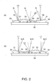
- FIGs. 2(a) and 2(b) are partially enlarged views of the tilt-mirror device 30.
- Fig. 2(a) is a drawing showing a configuration, in which the G-ray from the first color-ray light source 10 is modulated.
- the tilt-mirror device 30 is provided with a plurality of movable mirror elements 31 disposed on the surface.
- the movable mirror element 31 is rotatable around a predetermined shaft 35.
- two electrodes 33 and 34 are arranged in the vicinity of the periphery of one movable mirror element 31.
- the driving control unit 40 drives the movable mirror element 31 corresponding to an image signal to the first reflection position or the second reflection position arranged substantially symmetrically with the first reflection position around the predetermined shaft 35.
- the movable mirror elements 31 in the right and left are located at the first reflection position.
- the central movable mirror element 31 in Fig. 2(a) is located at the second reflection position.
- the driving control 40 drives the tilt-mirror device 30 so as to locate the movable mirror element 31 corresponding to the pixel at the first reflection position.
- the driving control 40 drives the tilt-mirror device 30 so as to locate the movable mirror element 31 corresponding to the pixel at the second reflection position.
- the G-ray can be modulated into light (ON) proceeding in the predetermined L1 direction and light (OFF) proceeding in the L2 direction in response to an image signal.
- the second color-ray light source 20 is configured so that if the movable mirror element 31 is located at the second reflection position, the R-ray or B-ray is reflected in the predetermined L1 direction, while if the movable mirror element 31 is located at the first reflection position, the R-ray or B-ray is reflected in an L3 direction different from the predetermined L1 direction.
- the driving control 40 drives the tilt-mirror device 30 so as to locate the movable mirror element 31 corresponding to the pixel at the second reflection position.
- the driving control 40 drives the tilt-mirror device 30 so as to locate the corresponding movable mirror element 31 at the first reflection position.
- an image signal corresponding to an R-image or a B-image designates ON of a pixel
- color light from the R-ray light-emitting element 21 or the B-ray light-emitting element 22 is guided in the L1 direction by the movable mirror element 31 corresponding to the pixel.
- an image signal corresponding to the R-image or the B-image designates OFF of a pixel
- color light from the R-ray light-emitting element 21 or the B-ray light-emitting element 22 is guided in the L3 direction different from the L1 by the movable mirror element 31 corresponding to the pixel.
- the R-ray or the B-ray can be modulated into light (ON) proceeding in the predetermined L1 direction and light (OFF) proceeding in the L3 direction in response to an image signal.
- the respective movable mirror elements 31 in the tilt-mirror device 30 modulates the R-ray, B-ray, and G-ray during one frame period by a PWM (pulse width modulation) method so as to depict colors and brightness of the entire pixels in the frame.
- PWM pulse width modulation
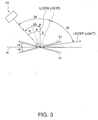
- the relationship between the inclined angle relative to a plane defined by arrays of a plurality of the movable mirror elements 31 (referred to below as a horizontal plane H) and the reflection angle will be described with reference to Fig. 3.
- the movable mirror element 31 is assumed to be rotatable at an angle of ⁇ ⁇ relative the horizontal plane H.
- the predetermined L1 direction (ON) is angled at 2 ⁇ relative to the light from the first color-ray light source 10.
- the predetermined L2 direction (OFF) is angled at 6 ⁇ relative to the light from the first color-ray light source 10.
- the respective light sources are arranged so that the predetermined L1 direction (ON) of light from the first color-ray light source 10 is aligned with the predetermined L1 direction (ON) of light from the second color-ray light source 20.
- the predetermined L2 direction in which light from the first color-ray light source 10 is reflected as OFF light, is angled at 60 relative to light from the first color-ray light source 10.
- the predetermined L3 direction in which light from the second color-ray light source 20 is reflected as OFF light, is also angled at 60 relative to light from the second color-ray light source 20.
- the predetermined L2 and L3 directions are symmetrical with each other about the predetermined L1 direction.
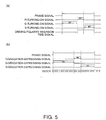
- Fig. 5(a) is a drawing showing the turning-on period and timing.
- the charts in Fig. 5(a) indicate a "frame signal”, “R-turning-on signal”, “G-turning-on signal”, “B-turning-on signal”, and “driving polarity inversion signal”. The time is plotted in the horizontal axis of the chart.
- the high-period of the "frame signal” indicates the period of one frame of an image signal.
- the high-period of the "R-turning-on signal” means the turning-on period of the R-ray light-emitting elements 21 (turning-on period RT), which agrees with a sub-frame period of images corresponding to the R-ray.
- the high-period of the "G-turning-on signal” means the turning-on period of the G-ray light-emitting elements 11 (turning-on period GT), which agrees with a sub-frame period of images corresponding to the G-ray.
- the high-period of the "B-turning-on signal” means the turning-on period of the B-ray light-emitting elements 22 (turning-on period BT), which agrees with a sub-frame period of images corresponding to the B-ray.
- the "driving polarity inversion signal” is a signal showing to locate the movable mirror element 31 whether at the first reflection position or at the second reflection position when the pixel (on a screen) is to be ON.
- the high-period of the "driving polarity inversion signal" designates to locate the movable mirror element 31 at the second reflection position when the pixel is to be ON, while the low-period designates to locate the movable mirror element 31 at the first reflection position when the pixel is to be ON.
- the G-ray light-emitting element 11 is turned on for the predetermined turning-on period GT, and the R-ray light-emitting element 21 is turned on for the turning-on period RT after the turning-on period GT is finished.
- the B-ray light-emitting element 22 is turned on for the predetermined turning-on period BT after the turning-on period RT is finished.
- the driving polarity inversion signal is in the low state for the turning-on period GT. That is, the driving polarity inversion signal locates the movable mirror element 31 at the first reflection position when the pixel is to be ON for this period.
- the driving polarity inversion signal is in the high state for the turning-on period RT and the turning-on period BT. That is, the driving polarity inversion signal locates the movable mirror element 31 at the second reflection position when the pixel is to be ON for this period.
- the driving control unit 40 serving also as a light source driver turns on the R-ray light-emitting element 21, the G-ray light-emitting element 11, and the B-ray light-emitting element 22 by sequentially switching them in turn.
- An observer can recognize the R-ray, the G-ray, and the B-ray in the integrated state with time, obtaining full-color images.
- the turning-on periods GT, RT, and BT of each color light-emitting element are independently differed from each other within one frame of displayed images. Thereby, even when the amount of the luminous flux of each light source differs, appropriate images can be displayed. In the example in Fig. 5(a), the turning-on periods GT is longest, the turning-on periods BT is next longer, and the turning-on periods RT is shortest.
- the G-ray have 60% to 80% of the entire luminous flux amount for obtaining white light.
- the turning-on period GT of the G-ray light-emitting element 11 is increased longer than the turning-on period RT of the R-ray light-emitting element 21 and the turning-on period BT of the B-ray light-emitting element 22.
- the driving control unit 40 drives the movable mirror element 31 to the first reflection position during the turning-on of the G-ray light-emitting element 11. Furthermore, in order to guide the R-ray or B-ray in the predetermined direction L1, the driving control unit 40 drives the movable mirror element 31 to the second reflection position during the turning-on of the R-ray light-emitting element 21 or the B-ray light-emitting element 22.
- the reflection position (first reflection position) of the movable mirror element 31 when the G-ray is guided in the predetermined direction L1 is opposite in position to the reflection position (second reflection position) of the movable mirror element 31 when the R-ray or B-ray is guided in the predetermined direction L1. Therefore, as shown in the driving polarity inversion signals in Fig. 5(a), the driving polarity of the G-ray light-emitting element 11 for the movable mirror element 31 is inverted from that of the R-ray light-emitting element 21 or the B-ray light-emitting element 22. Thereby, the R-ray, the G-ray, and the B-ray can be modulated in contents whether they are guided to the predetermined direction.
- Fig. 5(b) is a drawing showing the drive timing of the tilt-mirror device 30.
- Fig. 5(b) shows timing charts of a "frame signal", “R-gradation expressing signal”, “G-gradation expressing signal”, “B-gradation expressing signal”, and “clock”. The time is plotted in the horizontal axis of the charts. More specifically, the high-period of the "R-gradation expressing signal” corresponds to a gradation-expressing period RK, the high-period of the "G-gradation expressing signal” corresponds to a gradation-expressing period GK, and the high-period of the "B-gradation expressing signal” corresponds to a gradation-expressing period BK.
- RK gradation-expressing period
- G-gradation-gradation expressing signal corresponds to a gradation-expressing period GK
- B-gradation expressing signal corresponds to a gradation-expressing period BK.
- the gradation-expressing period GK arises at first, the gradation-expressing period RK continues after the gradation-expressing period GK is finished, and then, the gradation-expressing period BK arises after the gradation-expressing period RK is finished.
- the duration of the gradation-expressing period GK is longest and the gradation-expressing period RK is shortest.
- the gradation-expressing period GK is the duration necessary for achieving the optical power (gradation) of the G-ray by the spatial light modulation device (tilt-mirror device 30). Also, the gradation-expressing period GK agrees with a sub-frame period of images corresponding to the G-ray. Within the gradation-expressing period GK, incident light is modulated corresponding to an image signal by a method of pulse-duration modulation. More specifically, if the image signal designates the optical power of the G-ray with n-bits (n is a positive integer), the gradation-expressing period GK is divided into n unit periods with a length ratio of 2 0 : 2 1 : ... :, : 2 (n-1) .
- the movable mirror element 31 maintains any one of the ON state and OFF state in each of the n unit periods.
- the movable mirror element 31 may be turned on for the necessary unit periods of the n unit periods so that incident light proceeds in the direction L1 for the time proportional to its optical power. For example, if the maximum value of the optical power designated by an image signal is ((2 n ) - 1), for the entire n unit periods, i.e., for substantially the entirety of the gradation-expressing period GK, the mirror may be in the ON state.
- the mirror may be in the OFF state.
- the gradation-expressing period RK and the gradation-expressing period BK are the same as the gradation-expressing period GK, the description is omitted.
- the position of the movable mirror element 31 in the ON state in the gradation-expressing period RK and the gradation-expressing period BK is different from the position of the movable mirror element 31 in the ON state in the gradation-expressing period GK.
- lengths of these gradation-expressing periods RK, GK, and BK may be different. If the lengths of the gradation-expressing periods RK, GK, and BK are different, the respective unit periods divided into the n units also differs corresponding to the each color light of R, G, and B.
- the gradation-expressing period RK substantially agrees with the turning-on period RT shown in Fig. 5(a).
- the gradation-expressing period GK substantially agrees with the turning-on period GT shown in Fig. 5(a).
- the gradation-expressing period BK substantially agrees with the turning-on period BT shown in Fig. 5(a).
- the entire movable mirror elements 31 are driven according to the timing charts shown in Fig. 5(b).
- the driving control unit 40 can differentiate the frequency of a G-ray light-source driving clock signal when driving the G-ray light-emitting element 11 from the frequency of a second-ray light-source driving clock signal when driving the R-ray light-emitting element 21 or the B-ray light-emitting element 22. Thereby, the light source can be appropriately driven for each color. Furthermore, it is more preferable that the G-ray light-source driving clock signal and the second-ray light-source driving clock signal have a unit clock signal with the frequency common to both the signals. Thereby, the driving circuit can be simplified.
- the turning-on period or the gradation-expressing period for the G-ray may be controlled to be larger than the other rays.
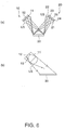
- Fig. 6(a) is a drawing of the configuration of the light source supplying illumination light.
- part of the configuration such as the movable mirror element is omitted for brevity.
- the first color-ray light source 10 and the second color-ray light source 20 have a plurality of the light-emitting elements 11, 21, and 22 for each color, respectively. Also, these light-emitting elements 11, 21, and 22 for each color have light-emitting chips 12, 24 and 25; and a lens member LS for guiding light-source light from the light-emitting chips 12, 24 and 25 to substantially the entire region of the tilt-mirror device 30; respectively.
- a plurality of the R-ray light-emitting elements 21 and a plurality of the B-ray light-emitting elements 22 are mounted on a common substrate 23. Thereby, the light-emitting element with the large luminous flux amount can be efficiently emitted in its own.
- Fig. 6(b) is a drawing showing the configuration of the light-emitting element more in detail using the G-ray light-emitting element 11 as a typical example.
- the G-ray light-emitting element 11 comprises a tapered rod member 13 for guiding light-source light to the tilt-mirror device 30, which is directed in the predetermined direction.
- a reflection surface is formed inside the tapered portion.
- the light-emitting chip 12 can be efficiently emitted, and the tilt-mirror device 30 is efficiently illuminated, obtaining bright images.
- the light-emitting chip 12 be formed integrally with the lens member LS. The manufacturing is thereby facilitated while unevenness of light intensity of each light-emitting element can be reduced.
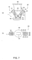
- FIG. 7(a) and 7(b) A projector according to a second embodiment of the present invention will be described with reference to Figs. 7(a) and 7(b). Like reference characters designate like portions common to the first embodiment described above and tautological description is omitted.
- the image display device 1 Out of the modulated light by the image display device 1 described above, only the light proceeding in the predetermined direction L1 (see Figs. 2(a) and 2(b).) enters a projection lens 50. Whereas the light proceeding in the direction L2 or L3 (see Figs. 2(a) and 2(b).) does not enter the projection lens 50 and is discarded.
- the projection lens 50 projects an image displayed by the image display device 1 corresponding to an image signal on a screen 60. An observer of the screen 60 recognizes the image as a full color image.
- FIG. 8 is a drawing showing a summarized configuration of a projector 100 having an image display device according to a third embodiment of the present invention.
- a light-source 110 comprises a G-ray light-emitting element 110G for supplying a G-ray, which is a first color-ray in a first wavelength region; an R-ray light-emitting element 110R for supplying an R-ray, which is a second color-ray in a second wavelength region different from the first wavelength region; and a B-ray light-emitting element 110B for supplying a B-ray.
- a G-ray light-emitting element 110G for supplying a G-ray, which is a first color-ray in a first wavelength region
- an R-ray light-emitting element 110R for supplying an R-ray, which is a second color-ray in a second wavelength region different from the first wavelength region
- a B-ray light-emitting element 110B for supplying a B-ray.
- a driving control unit 130 drives and controls the light-emitting elements for each color-ray 110R, 110G, and 110B and the tilt-mirror device 140. This driving control will be described later in detail.
- the surface of the tilt-mirror device 140 is provided with a plurality of movable mirror elements 141 arranged thereon.
- the movable mirror element 141 is rotatable around a predetermined shaft (not shown). Then, the movable mirror element 141 is inclined about the predetermined shaft as a center so as to selectively have two positional states of a first reflection position and a second reflection position.
- the driving control unit 130 drives the movable mirror element 141 corresponding to an image signal to between the first reflection position and the second reflection position, which is substantially symmetrical with the first reflection position about the predetermined shaft. For example, if the movable mirror element 141 is located at the first reflection position, the reflected light from the movable mirror element 141 proceeds in a direction incident in a projection lens system 150. The incident light in the projection lens system 150 is projected on a screen 160.
- the reflected light from the movable mirror element 141 proceeds in a direction other than that of the projection lens system 150.
- the reflected light is not projected on the screen 160.
- incident light can be modulated and reflected corresponding to an image signal.
- one light source 110 is provided on one side of the projection lens 150.
- the turning-on period and timing according to the embodiment are the same as those described with reference to Figs. 5(a) and 5(b), though the driving polarity inversion time signal in Fig. 5(a) is not necessary in this embodiment.
- the driving control unit 130 serving also as a light source driver turns on the R-ray light-emitting element 110R, the G-ray light-emitting element 110G, and the B-ray light-emitting element 110B by sequentially switching them. Within one frame of displayed images, the turning-on period of each color-ray light-emitting element is differentiated.
- the luminous flux amount can be thereby set arbitrarily. As a result, a compact and bright image display device using a spatial modulation element can be provided. Also, even when the luminous flux amount of each light source is different, more bright images can be displayed.
- the luminous flux amount of the G-ray be about 60% to 80% of the entire luminous flux amount. Therefore, a turning-on period GT of the G-ray light-emitting element 110G is increased longer than a turning-on period RT of the R-ray light-emitting element 110R and a turning-on period BT of the B-ray light-emitting element 110B. Thereby, even the G-ray light-emitting elements 110G, the R-ray light-emitting elements 110R, and the B-ray light-emitting elements 110B are the same in power and the number, the luminous flux amount of the G-ray necessary for obtaining white light can be obtained while the light source is miniaturized.
- the number of the G-ray light-emitting elements 110G, the R-ray light-emitting elements 110R, and the B-ray light-emitting elements 110B are substantially the same is now discussed.
- the spatial expanses of the light-sources for each color are substantially the same.
- the luminous flux amount of the G-ray be about 60% to 80% of the entire luminous flux amount.
- the G-ray light-emitting elements 110G are turned on for a period longer than the other light-emitting elements, so as to increase a gradation-expressing period GK of the G-ray longer than a R-gradation expressing period RK and a B-gradation expressing period BK.
- the G-ray light-emitting elements 110G, the R-ray light-emitting elements 110R, and the B-ray light-emitting elements 110B are the same in power and the number, the luminous flux amount of the G-ray necessary for obtaining white light can be obtained while the light source is miniaturized.
- the unit-bit length of the G-gradation-expressing period GK is different from the unit-bit length of the R-gradation-expressing period RK or the B-gradation-expressing period BK.
- the driving control unit 130 can differentiate a frequency of a G-ray light-source driving clock signal when driving the G-ray light-emitting elements 110G from a frequency of a second color-ray light-source driving clock signal when driving the R-ray light-emitting elements 110R or the B-ray light-emitting elements 110B. Thereby, appropriate light-source driving can be performed in each color-ray.
- the G-ray light-source driving clock signal and the second color-ray light-source driving clock signal further have a unit clock signal with a frequency common to both the signals.
- the driving circuit can be simplified.
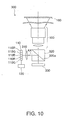
- Fig. 9 is a drawing showing a summarized configuration of a projector 200 having an image display device according to a fourth embodiment of the present invention. It is different from the third embodiment described above in that a transmissive liquid crystal light valve 210 is used as a spatial modulation element. Like reference characters designate like portions common to the first embodiment and tautological description is omitted.
- the light source 110 turns on the light-emitting elements for each color-ray 110R, 110G, and 110B with the timing shown in Fig. 5.
- Light from these light-emitting elements illuminates a transmissive liquid crystal light valve 210 crowdedly by means of the fly-eye lens array 120.
- Light incident in the transmissive liquid crystal light valve 210 is modulated and emitted by being transmitted or non-transmitted (shielded) corresponding to an image signal.
- the modulated light from the transmissive liquid crystal light valve 210 is projected on the screen 160 via the projection lens system 150.
- Fig. 10 is a drawing showing a summarized configuration of a projector 300 having an image display device according to a fifth embodiment of the present invention. It is different from the fourth embodiment described above in that a reflective liquid crystal light valve is used as a spatial modulation element. Like reference characters designate like portions common to the fourth embodiment and tautological description is omitted.
- the light source 110 turns on the light-emitting elements for each color-ray 110R, 110G, and 110B with the timing shown in Fig. 5.
- Light from these light-emitting elements is converted into S-polarization light by a polarization changer (not shown).
- the S-polarization light is reflected on a polarization surface 320a of a polarization beam splitter 320.
- the polarization surface 320a has an angular response about the polarization split. Therefore, principal light beams from the light-emitting elements for each color-ray 110R, 110G, and 110B are converted by a lens 310 so as to be substantially in parallel with an optical axis AX.
- the light reflected on the polarization surface 320a enters a reflective liquid crystal light valve 330.
- the reflective liquid crystal light valve 330 modulates the S-polarization light into a P-polarization light so as to be emitted corresponding to an image signal.
- the P-polarization light which is modulated light
- the S-polarization light which is non-modulated light
- the S-polarization light is reflected on the polarization surface 320a toward the light source 110 and is discarded.
- the modulated light is projected on the screen 160 by the projection lens system 150. Bright full-color images can be thereby projected with a compact light source.
- Fig. 11 is a drawing showing a summarized configuration of an image display device 400 according to a sixth embodiment of the present invention.
- Like reference characters designate like portions common to the embodiments described above and tautological description is omitted.
- a direct-viewing image display device is provided.
- Each color-ray from the light source 110 enters a light-guide plate 410 as a backlight ray.
- the backlight ray enters a transmissive liquid crystal light valve 420 as a spatial modulation element via the light-guide plate 410.
- the transmissive liquid crystal light valve 420 modulates incident light to be emitted by transmission or non-transmission thereof corresponding to an image signal. Thereby, full-color images can be obtained when being viewed in the direction A.
- a projector having a solid light-emitting element such as a light-emitting diode as a light source according to a seventh embodiment will be described.
- the life of the light source itself is long and maintenance due to a burned-out light bulb is not necessary.
- color balance can be adjusted by the adjustment of on-off timing for each color.
- a color filter is not necessary and light is efficiently utilized without noise. Therefore, by adopting the solid light-emitting element as a light source, a compact projector capable of projecting high-quality bright color images can be provided.
- each individual solid light-emitting element is a semiconductor light-emitting element, it is small in size, so that the light quantity necessary for an illumination device may be provably obtained by arranging a plurality of the elements two-dimensionally in an array or in a matrix arrangement.
- each individual solid light-emitting element has an area, although it is small in size, if a number of solid light-emitting elements are arranged for acquiring quantity of light, the area of a light-emitting region of the illumination device is consequently increased, and an optical system for condensing the illumination luminous flux from the illumination device on a light valve is also increased in size and complicated, so that advantages of the solid light-emitting element are reduced. Furthermore, in the optical system for condensing the illumination luminous flux, various aberrations such as astigmatism and chromatic aberration may be produced so that it becomes rather difficult to project clear color images.
- the spatial modulation device (light valve)
- the light modulated by the spatial modulation device (light valve)
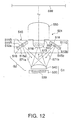
- Fig. 12 shows a summarized configuration of a projector 501 according to the present invention having LED elements, which are solid light-emitting elements, used for a light emitting source.
- the projector 501 according to the embodiment comprises a light source 510 having a plurality of the LED elements, a light valve 530, which is a reflection type spatial light modulation device, having a modulation region (reflection surface) 539 for forming images by switching an illumination luminous flux (incident luminous flux) 571a from the light source 510, and a projection lens 550 for projecting a display luminous flux 573, which is formed by modulating the illumination luminous flux 571, on a screen 599.
- a light source 510 having a plurality of the LED elements
- a light valve 530 which is a reflection type spatial light modulation device, having a modulation region (reflection surface) 539 for forming images by switching an illumination luminous flux (incident luminous flux) 571a from the light source 510
- the reflection light valve 530 is a micro-mirror device having a modulation region or an image-forming region 539 having tilt-mirror elements (switching elements), which are movable elements, each having a plurality of micro-rectangular and mirror-finished modulation surfaces (micro-mirrors), arranged in an array or a matrix arrangement.
- switching elements tilt-mirror elements
- micro-mirrors micro-rectangular and mirror-finished modulation surfaces
- a micro-mirror 531 is rotatably supported on a semiconductor substrate 535 with a column 534, so that inclination of the micro-mirror 531 is to be controlled using a pair of address electrodes 536a and 536b disposed on the surface of the semiconductor substrate 535 as actuators.
- the micro-mirror 531 is rotated about the column 534 as a center from the horizontal position in a predetermined direction within a range of about ⁇ 10° so as to be an ON-position at each position.
- the switching element 532 comprises two orientations 537a and 537b inclined about the column 534 in the right and left, so that if there is the illumination luminous flux 571 incident from the inclined direction, it is reflected in the direction toward the projection lens 550 as effective light, i.e., the display luminous flux 573.
- the switching element 532 when the switching element 532 is at an oriented state 537a, it is in an ON-state (a state of the reflected luminous flux incident in the projection lens), while being at an oriented state 537b, it is in an OFF-state (a state of the reflected luminous flux not incident in the projection lens).
- the switching element 532 when the switching element 532 is at an oriented state 537b, it is in an ON-state (a state of the reflected luminous flux incident in the projection lens), while being at an oriented state 537a, it is in an OFF-state (a state of the reflected luminous flux not incident in the projection lens).
- the projector 501 further comprises a field lens 540 with positive refracting power, which is arranged close to the projection lens 550 in the vicinity of the light valve 530 so that the illumination luminous flux 571 and the display luminous flux 573 pass therethrough. That is, the field lens 540 is located in between the projection lens 550 and the light valve 530. Also, the field lens 540 is positioned on an optical path connecting between the projection lens 550 and the light valve 530.
- the field lens 540 functions to condense the illumination luminous flux 571 outputs from the light source 510 on the light valve 530, while to the display luminous flux 573, it functions to condense the display luminous flux 573 on the screen 599 together with the projection lens 550. Furthermore, between the light source 510 and the projection lens 550, an optical system is defined, which is constituted of the field lens 540 and the modulation region 539 of the reflection light valve 530. In this specification, this optical system is referred as a modulation optical system G1.
- the light source 510 comprises two light-emitting regions 512a and 512b arranged by sandwiching an incident end of the projection lens 550 therebetween so as to be directed toward the field lens 540.
- the light-emitting regions 512a and 512b are substantially the same in shape and size; however, one light-emitting region (first light-emitting region) 512a is provided with a plurality of red LED elements (solid light-emitting elements) 511R and a plurality of blue LED elements 511B arranged thereon, while the other light-emitting region (second light-emitting region) 512b is provided with only a plurality of green LED elements 511G arranged thereon.
- the entire of the plurality of micro-lenses 516 correspond to the light-emitting regions 512a and 512b.
- the entire light emitting section 513 of the LED elements 511 corresponds to the light-emitting regions 512a and 512b.
- An optical system (referred to as an illumination optical system in the specification) G2 constituted of the respective micro-lenses 516 and the field lens 540 guides the illumination luminous flux 571 from each of the LED elements 511 to the modulation region 539 of the light valve 530.
- the modulation optical system G1 including the field lens 540 and the light valve 530 guides the illumination luminous flux 571 from the light-emitting regions 512a and 512b (micro-lens arrays 512a and 512b according to the embodiment) to an entrance pupil 552 of the projection lens 550.
- the light-emitting regions 512a and 512b are arranged in an optically conjugate relationship to the entrance pupil 552 of the projection lens 550 with the modulation optical system G1 including the field lens 540 and the light valve 530 therebetween. More specifically, the light-emitting regions 512a and 512b are located on a virtual plane optically conjugated to the entrance pupil 552 with the modulation optical system G1 including the field lens 540 and the light valve 530 therebetween. The entire rays are restricted by the entrance pupil 552 viewed from an incident side 551 of the projection lens 550.
- conjugate images 515i of the light-emitting regions 512a and 512b are formed in the entrance pupil 552. That is, the entire illumination luminous flux 571a or 571b output from the light-emitting region 512a or 512b, except losses due to reflection and absorption of the field lens 540 and absorption of the light valve 530, enters the projection lens 550 via a diaphragm 559 so as to be projected on the screen 599.
- the illumination luminous fluxes 571a and 571b output from the light-emitting regions 512a and 512b are efficiently utilized for projecting images on the screen 599. Accordingly, the projector 501 capable of displaying most bright images with minimum areas of the light-emitting regions 512a and 512b can be provided.
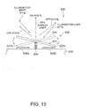
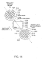
- the switching element 532 constituting the modulation region 539 of the light valve 530 is provided with two positions 537a and 537b. Therefore, when the light valve 530 is turned ON, there are two positions conjugate to the entrance pupil 552. As shown in Fig. 14, positions L1 and L2, which are symmetrical about a rotating direction (switching direction) S of the micro-mirror 531 of the switching element 532 and sandwiching the entrance pupil 552 therebetween, are positions conjugated to the entrance pupil 552. That is, in the direction passing through the center 530c of the light valve 530 and being inclined at 45° relative to one side 530a of the light valve 530, the first and second light-emitting regions 512a and 512b are located.
- This direction inclined at 45° relative to the light valve 530 is the switching direction of the switching element 532 of the light valve 530, in which the micro-mirror 531 rotates, and is an incident direction of the illumination luminous flux 571.
- the ranges of images 552i of the entrance pupil 552 formed at the positions L1 and L2 conjugated to each other with the modulation optical system G1 therebetween are regions arranged in a conjugate relationship to the entrance pupil 552. Then, in the ranges of the images 552i conjugated to the entrance pupil 552 and formed symmetrical about the switching direction S, the LED elements 511R and 511B/511G are arranged to form the first and second light-emitting regions 512a and 512b, respectively.
- the projector 501 is provided with the first and second light-emitting regions 512a and 512b conjugated to the entrance pupil 552 of the projection lens 550 by arranging the field lens 540 with a convex lens effect and positive refracting power in the vicinity of the light valve 530. Furthermore, by arranging the LED elements 511R and 511B/511G on these regions 512a and 512b, respectively, light emitted from a plurality of the LED elements can efficiently enter the projection lens 550.
- LED elements with high brightness and high power have been put in practical application for various light sources, including the blue LED elements 511B in particular.
- the light quantity of the individual LED element is extremely small in comparison with a conventional white lamp, so that it is preferable to arrange a plurality of the LED elements for acquiring sufficient quantity of light necessary for the projector 501. Even when a number of the LED elements are arranged, if substantially the entire light output therefrom is not used for projecting images to a screen, this is wasteful and increasing power consumption and size.
- the LED elements 511 are arranged on the regions 512a and 512b conjugated to the entrance pupil 552, so that light emitted from the LED elements 511 is not wastefully used and is efficiently utilized. Accordingly, the highly compact and energy-saving projector 501 capable of projecting brightest images can be achieved.
- the LED elements 511R, 511G, and 511B may also be arranged. Even in this case, light emitted from the respective LED elements efficiently enters the projection lens 550, enabling a compact projector capable of projecting bright images to be achieved by using light efficiently. However, if both the conjugate regions 512a and 512b are used, the area for arranging the LED elements 511 is doubled, enabling further bright images to be displayed.
- the LED elements 511R (red), 511G (green), and 511B (blue) may be arranged at the same rate, wherein by controlling two ON-states 537a and 537b of the switching element 530 simultaneously with each color-ray from two regions 512a and 512b emitted in a time-shared system, multi-color images can be displayed. Since the illumination luminous fluxes 571a and 571b are respectively emitted from the two-way regions 512a and 512b, if the number of switching elements 532 corresponding to each color-ray or at least two color-rays are prepared on the modulation region 539, two-color images can also be output simultaneously.
- the ON oriented states 537a and 537b may be controlled for each color, so that the control of the switching elements 532 is extremely simplified, enabling bright images to be displayed with the small number of the switching elements.
- a balance of the number of light-emitting elements for each color be set to have white light in view of spectral luminous efficiency.
- the spectral luminous efficiency is very small for green, and the power of the green-ray LED element 511G has not been improved enough to cover the spectral luminous efficiency.
- the green-ray LED elements 511G with the low spectral luminous efficiency are independently arranged on the second light-emitting region 512b, while the red-ray LED elements 511R and the blue-ray LED elements 511B are arranged on the first light-emitting region 512a, so as to acquire the color balance.
- the respective light-emitting regions 512a and 512b are located on visual planes conjugated to the entrance pupil 552. Therefore, if the LED elements 511 are efficiently arranged on the conjugated images 552i of the entrance pupil 552 produced on the conjugated virtual planes, the illumination luminous flux 571 output from the LED elements 511 can be efficiently utilized for projecting images without being wasted. Accordingly, in order to display bright images, shapes of the light-emitting regions 512a and 512b may be brought into agreement with shapes of the conjugated images 552i, respectively.
- the light-emitting regions 512a and 512b are located within ranges of the conjugated images 552i of the entrance pupil 552.
- the conjugated images 552i of the entrance pupil 552, i.e., ranges within circles indicated by dotted lines in Fig. 14 may be filled with the LED elements 511 including the micro-lenses 516.
- the LED elements 511 are arranged in an array on the first light-emitting region 512a so as to fill the images 552i of the entrance pupil with the LED elements 511. Since part of the light-emitting region 512a of the LED elements 511 is protruded out of the conjugated images 552i, wasteful light is produced. Although part of the conjugated images 552i is not overlapped on the light-emitting region 512a, in this arrangement, a number of the LED elements 511 can be easily arranged methodically.
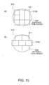
- Fig. 15(b) shows an arrangement of the LED elements 511 where the elements are horizontally or vertically shifted by a half pitch (may be less than a half pitch).
- a half pitch may be less than a half pitch.
- the LED elements 511 are arranged, so that the illumination flux 571 can be prevented from being wasted and the compact projector 501 capable of displaying bright images can be provided.
- the LED elements 511 there is dispersion in the light power output from the individual LED elements 511.
- the micro-lens array 515 is arranged so that the light emitting sections 513 of the LED elements 511 are conjugated to the modulation region 539 of the light valve 530 with the illumination optical system G2 therebetween, which includes the micro-lens 516 constituting the micro-lens array 515 and the field lens 540.
- the light emitting section 513 is conjugated to the modulation region 539, so that the modulation region 539 is efficiently illuminated with the illumination luminous flux 571 emitted from the light emitting section 513. Therefore, even in a microscopic region of the individual LED element 511, light output from the LED element 511 can be prevented from being wasted, enabling a compact projector 501 capable of displaying more bright images to be provided.
- each of the light emitting section 513 is conjugated to the modulation region 539, the entire modulation region 539 is illuminated with the illumination luminous flux 571 emitted from the light emitting section 513 of the individual LED element 511. Accordingly, the individual difference of light power output from the individual LED element 511 is cancelled, so that the modulation region 539 can be efficiently illuminated with a plurality of LED elements 511 further without dispersion. Therefore, the images projected to the screen 599 can be improved not only in brightness but also in image quality by eliminating image dispersion.
- the shape of the individual light emitting section 513 be analogous to that of the modulation region 539. That is, it is preferable that the length-and-breadth ratio (aspect ratio) of the light emitting section 513 be identical to that of the modulation region 539. It is also preferable that one side 539a of the modulation region 539 be arranged in parallel to the crosswise side 513a of the light emitting section 513. Therefore, according to the embodiment, the LED elements 511, each having a rectangular light emitting section 513 with a size of about 2 mm ⁇ 3 mm, are arranged on the first and second light-emitting regions 512a and 512b.
- the shape of the individual light emitting section 513 is not limited to be analogous to that of the modulation region 539.
- the light emitting section 513 can be conjugated to the modulation region 539.
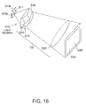
- the micro-lens 516 shown in Fig. 16 is formed to be different in lengthwise and lateral curvatures or magnification, and when passing through the illumination optical system G2, the cross-section of the illumination luminous flux 571 becomes rectangular, so that the entire modulation region 539 of the light valve 530 is illuminated therewith. Since the micro-lens 516 produces astigmatism, the image-formation position in the lengthwise direction does not agree with that in the lateral direction.
- the illumination optical system G2 is designed so as to arrange the light valve 530 between the image-formation position in the lengthwise direction 513y of the light emitting section 513 and the image-formation position in the lateral direction 513x of the light emitting section 513, substantially the entire modulation region 539 can be illuminated with the illumination luminous fluxes 571 emitted from the individual light emitting sections 513, suppressing the illumination luminous flux from being wasteful to the minimum.
- each of the LED elements 511 has an extremely microscopic and square light-emitting section 513 with a size of about 1 mm ⁇ 1 mm, for example, it is difficult to conjugate the light emitting sections 513 to the modulation region 539 in the illumination optical system G2.
- the light-emitting section 513 is square or rectangular, there are advantages for each case.
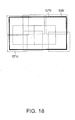
- the modulation region 539 can be illuminated so that images 571i of the light-emitting sections 513 overlap the modulation region 539, as shown in Fig. 18.
- the microscopic light-emitting surface 513 is square, since the images 571i formed on the modulation region 539 are also square, it is easy to align a side of the modulation region 539 with a side of the images 571i of the light-emitting section 513, preventing the illumination luminous flux 571i from being wasteful.
- the light-emitting section 513 is analogous to the modulation region 539 or is rectangular close thereto, by aligning the longitudinal side of the light-emitting section 513 with the longitudinal side of the modulation region 539, the shape of the modulation region 539 can be easily aligned with the entire cross-section of the illumination luminous flux 571 supplied from the light-emitting region 512a, enabling efficient illumination to be performed.
- the LED elements 511 are necessary to be arranged so that the longitudinal side of the light-emitting section 513 is to be parallel with the longitudinal side of the modulation region 539.
- the individual light-emitting sections 513 are not conjugated to the modulation region 539 with the illumination optical system G2 therebetween, in such a manner, by forming the light-emitting section 513 to be square, or more preferably to be rectangular and analogous to the modulation region 539, wasteful light can be prevented from being produced by aligning edges of the illumination luminous flux 571. Furthermore, even in the projector without the field lens 540 arranged therein, by conjugating the light-emitting section 513 to the modulation region 539 with the illumination optical system G2 (only the micro-lens 516 in this case) therebetween, an advantage of eliminating wasteful illumination luminous flux is offered.
- a projector capable of displaying bright images can be provided even though it is compact and energy saving. Also, even in the case where the light-emitting section 513 is not conjugated to the modulation region 539 with the illumination optical system G2, by forming the shape of the light-emitting section 513 to be square, or to be rectangular and analogous to the modulation region 539, wasteful illumination luminous flux can be prevented as described above.
- the above-described example as shown in Fig. 19(a) by extending the modulation optical system G1 toward the illumination luminous flux 571 and the display luminous flux 573, is described based on a modulation optical system with the magnification of 1:1 between the illumination luminous flux, i.e., incident side, and the display luminous flux, i.e., emitting side.
- the luminous flux 571 is to be parallel in between the field lens 540 in the incident side and the field lens 540 in the emitting side (identical to the incident side). Therefore, the illumination luminous flux 571 illuminating the modulation region 539 becomes telecentric, facilitating to perform switching by changing the angle of the micro-mirror 531.
- the effective light can be separated from the non-effective light by an extremely small angle.
- the incident diameter of the projection lens 550 can be increased within the range of not taking the non-effective light therein, enabling more bright images to be displayed.
- the modulation optical system G1 in which the magnification of the emitting side is not identical to that of the incident side, can be adopted.
- the light source 510 in which the magnification of the emitting side relative to the incident side is 1 or more, the light source 510 is located closer to the light valve 530 than the projection lens 550.
- the modulation optical system G1 in which the magnification of the emitting side relative to the incident side is less than 1, 1/2 (0.5 times) for example, the illumination luminous flux 571 from the light source 510 is contracted by the field lens 540 so as to converge on the entrance pupil 552 of the projection lens 550.
- the area of the light-emitting region 512a or 512b is inversely increased relative to the entrance pupil 552, so that the light power of the illumination luminous flux 571 can be increased by arranging the more number of the LED elements 511.
- the modulation region 539 is illuminated with convergent light different from parallel light, so that effective light and non-effective light are not in parallel therewith.
- the aperture of the projection lens 550 can omit the non-effective light, there is no problem in image quality.
- the lightness of the lens may be possibly unchanged.
- the projector 501 is arranged so that the light source 510 is constituted of the LED elements 511R, 511G, and 511B, which are the solid light-emitting elements, and the light-emitting region 512 having a plurality of the LED elements arranged thereon is conjugated to the entrance pupil 552 of the projection lens 550 with the modulation optical system including the field lens 540 therebetween. Therefore, wasteful illumination luminous flux emitted from the light-emitting region 512 can be eliminated, so that there can be provided a compact and energy saving projector capable of displaying bright images with high quality by taking advantages of the solid light-emitting element.
- the light valve (the spatial light modulation device) 530 is a micro-mirror device or tilt-mirror device.
- a micro-mirror device tilt-mirror device a DMD (digital micro-mirror device) may be incorporated.
- the DMD is a device manufactured by Texas Instruments, Inc.
- the micro-mirror device is used for the light valve; however, it is not limited to this, and another light valve such as reflective liquid crystal may be used.
- the LED element is adopted as the solid light-emitting element; alternatively, other solid or semiconductor light-emitting elements such as an organic EL and semiconductor laser may be used.
- a projector using the solid light-emitting element as the light source and being capable of efficiently guiding the illumination luminous flux emitted from the solid light-emitting element to the projection lens. Therefore, it is possible to provide a projector capable of efficiently illuminating the light valve with the minimum configuration and also capable of projecting bright images with high quality on a screen even if it is compact and energy saving.
Landscapes
- Physics & Mathematics (AREA)
- General Physics & Mathematics (AREA)
- Engineering & Computer Science (AREA)
- Multimedia (AREA)
- Signal Processing (AREA)
- Optics & Photonics (AREA)
- Projection Apparatus (AREA)
- Non-Portable Lighting Devices Or Systems Thereof (AREA)
- Control Of Indicators Other Than Cathode Ray Tubes (AREA)
- Mechanical Light Control Or Optical Switches (AREA)
- Liquid Crystal (AREA)
Applications Claiming Priority (8)
| Application Number | Priority Date | Filing Date | Title |
|---|---|---|---|
| JP2002081598 | 2002-03-22 | ||
| JP2002081598 | 2002-03-22 | ||
| JP2002116689 | 2002-04-18 | ||
| JP2002116689 | 2002-04-18 | ||
| JP2002246921 | 2002-08-27 | ||
| JP2002246921 | 2002-08-27 | ||
| JP2003057503A JP4055610B2 (ja) | 2002-03-22 | 2003-03-04 | 画像表示デバイス及びプロジェクタ |
| JP2003057503 | 2003-03-04 |
Publications (2)
| Publication Number | Publication Date |
|---|---|
| EP1347653A2 true EP1347653A2 (de) | 2003-09-24 |
| EP1347653A3 EP1347653A3 (de) | 2005-08-03 |
Family
ID=27792245
Family Applications (1)
| Application Number | Title | Priority Date | Filing Date |
|---|---|---|---|
| EP03251840A Withdrawn EP1347653A3 (de) | 2002-03-22 | 2003-03-24 | Bildanzeigevorrichtung und Projektor |
Country Status (6)
| Country | Link |
|---|---|
| US (2) | US7165845B2 (de) |
| EP (1) | EP1347653A3 (de) |
| JP (1) | JP4055610B2 (de) |
| KR (1) | KR100559003B1 (de) |
| CN (2) | CN100351673C (de) |
| TW (1) | TWI221931B (de) |
Cited By (12)
| Publication number | Priority date | Publication date | Assignee | Title |
|---|---|---|---|---|
| WO2005078496A3 (en) * | 2004-02-11 | 2005-12-15 | 3M Innovative Properties Co | Reshaping light source modules and illumination systems using the same |
| EP1668916A1 (de) * | 2003-09-24 | 2006-06-14 | Infocus Corporation | Projektionsvorrichtung mit achsenparallelen mikrospiegeln und lichtquellen |
| WO2006019482A3 (en) * | 2004-07-21 | 2006-06-29 | 3M Innovative Properties Co | Projection system with scrolling color illumination |
| GB2434879A (en) * | 2006-02-07 | 2007-08-08 | Shinko Electric Ind Co | Miniaturized light source and mirror arrangement for an optical device |
| EP1737244A3 (de) * | 2005-06-20 | 2008-08-27 | Seiko Epson Corporation | Anzeigeeinheit und Lichtemissionseinheit |
| WO2009027903A3 (en) * | 2007-08-28 | 2009-04-30 | Koninkl Philips Electronics Nv | A front projector |
| EP1886185A4 (de) * | 2005-06-02 | 2009-07-15 | 3M Innovative Properties Co | System zur beleuchtung mehrerer orte und projektionsanzeigesystem damit |
| NL1031720C2 (nl) * | 2005-06-02 | 2011-07-26 | Samsung Electronics Co Ltd | Verlichtingsysteem in staat tot aanpassen van de beeldverhouding en een projectiesysteem dat gebruik maakt van het verlichtingsysteem. |
| EP2458875A1 (de) * | 2010-11-26 | 2012-05-30 | Sony Corporation | Beleuchtungseinheit, Projektionsanzeigeeinheit und Direktansichtsanzeigeeinheit |
| EP2700869A4 (de) * | 2011-04-22 | 2014-11-12 | Koito Mfg Co Ltd | Optische einheit |
| CN114373786A (zh) * | 2020-10-14 | 2022-04-19 | Oppo广东移动通信有限公司 | 显示装置及电子设备 |
| GB2556938B (en) * | 2016-11-28 | 2022-09-07 | Bae Systems Plc | Multiple waveguide structure for colour displays |
Families Citing this family (72)
| Publication number | Priority date | Publication date | Assignee | Title |
|---|---|---|---|---|
| JP3990251B2 (ja) * | 2002-10-11 | 2007-10-10 | Necディスプレイソリューションズ株式会社 | 投写型表示装置 |
| JP2004356579A (ja) * | 2003-05-30 | 2004-12-16 | Toshiba Corp | レーザ光出力装置、映像表示装置、および半導体レーザの駆動制御方法 |
| US7380947B2 (en) * | 2003-07-18 | 2008-06-03 | Texas Instruments Incorporated | Multi-step turn off mode for projection display |
| US8061856B2 (en) * | 2003-11-01 | 2011-11-22 | Silicon Quest Kabushiki-Kaisha | Projection apparatus and image projection changeover method |
| US8061854B2 (en) * | 2003-11-01 | 2011-11-22 | Silicon Quest Kabushiki-Kaisha | Projection display system with varying light source |
| US20090033878A1 (en) * | 2003-11-01 | 2009-02-05 | Akira Shirai | System configurations and methods for controlling image projection apparatuses and mirror device |
| US8462421B2 (en) * | 2003-11-01 | 2013-06-11 | Silicon Quest Kabushiki-Kaisha | System configurations and methods for controlling image projection apparatuses |
| US8228593B2 (en) * | 2003-11-01 | 2012-07-24 | Silicon Quest Kabushiki-Kaisha | System configurations and method for controlling image projection apparatuses |
| US8157389B2 (en) * | 2003-11-01 | 2012-04-17 | Silicon Quest Kabushiki-Kaisha | Synchronous control system for light source and spatial light modulator employed in projection apparatus |
| US7070301B2 (en) | 2003-11-04 | 2006-07-04 | 3M Innovative Properties Company | Side reflector for illumination using light emitting diode |
| US7450311B2 (en) * | 2003-12-12 | 2008-11-11 | Luminus Devices, Inc. | Optical display systems and methods |
| US7090357B2 (en) | 2003-12-23 | 2006-08-15 | 3M Innovative Properties Company | Combined light source for projection display |
| WO2005073952A1 (ja) * | 2004-01-28 | 2005-08-11 | Matsushita Electric Industrial Co., Ltd. | 発光方法、発光装置、投写型表示装置 |
| JP4665402B2 (ja) * | 2004-02-04 | 2011-04-06 | セイコーエプソン株式会社 | 投射型表示装置および投射型表示装置の制御方法、並びに投射型表示装置の制御プログラム |
| US7427146B2 (en) | 2004-02-11 | 2008-09-23 | 3M Innovative Properties Company | Light-collecting illumination system |
| US7300177B2 (en) | 2004-02-11 | 2007-11-27 | 3M Innovative Properties | Illumination system having a plurality of light source modules disposed in an array with a non-radially symmetrical aperture |
| GB0405747D0 (en) * | 2004-03-15 | 2004-04-21 | Imec Inter Uni Micro Electr | Projector system comprising pulsed light sources |
| JP4734843B2 (ja) * | 2004-03-31 | 2011-07-27 | ブラザー工業株式会社 | 3次元形状検出装置 |
| GB2414127A (en) * | 2004-05-12 | 2005-11-16 | Sharp Kk | Time sequential colour projection |
| US7101050B2 (en) | 2004-05-14 | 2006-09-05 | 3M Innovative Properties Company | Illumination system with non-radially symmetrical aperture |
| US7095547B2 (en) * | 2004-06-28 | 2006-08-22 | Aubuchon Christopher M | Multiple beam-directing micromirror device |
| US7390097B2 (en) | 2004-08-23 | 2008-06-24 | 3M Innovative Properties Company | Multiple channel illumination system |
| KR100677551B1 (ko) | 2005-01-05 | 2007-02-02 | 삼성전자주식회사 | Led 패키지, 조명계 및 이를 채용한 프로젝션 시스템 |
| JP5225688B2 (ja) * | 2005-01-06 | 2013-07-03 | トムソン ライセンシング | デジタル光プロジェクションシステムにおけるレインボーアーチファクトの低減 |
| US7450086B2 (en) * | 2005-03-14 | 2008-11-11 | Hewlett-Packard Development Company, L.P. | Projector |
| KR101199757B1 (ko) * | 2005-03-18 | 2012-11-08 | 엘지전자 주식회사 | 디스플레이장치 및 디스플레이방법 |
| US20060221019A1 (en) * | 2005-03-29 | 2006-10-05 | Texas Instruments Incorporated | Spatial light modulation display system |
| US20060250587A1 (en) * | 2005-05-05 | 2006-11-09 | Regis Grasser | Image projection method and projection system |
| TWI260923B (en) * | 2005-06-02 | 2006-08-21 | Benq Corp | Projector and color filtering device thereof |
| FR2887640B1 (fr) * | 2005-06-24 | 2008-10-03 | Thomson Licensing Sa | Procede d'illumination d'un imageur de projecteur, systeme et projecteur correspondant |
| US7492108B2 (en) * | 2005-08-11 | 2009-02-17 | Texas Instruments Incorporated | System and method for driving light-emitting diodes (LEDs) |
| DE102005054955A1 (de) * | 2005-08-31 | 2007-04-26 | Osram Opto Semiconductors Gmbh | Lichtemittierendes Modul, insbesondere zur Verwendung in einem optischen Projektionsgerät und optisches Projektionsgerät |
| DE102005061182B4 (de) * | 2005-12-21 | 2020-03-19 | Carl Zeiss Jena Gmbh | Beleuchtungseinrichtung zur Farbbildprojektion |
| US7530696B2 (en) * | 2006-02-13 | 2009-05-12 | Hewlett-Packard Development Company, L.P. | Projectors and operation thereof |
| US20070241340A1 (en) * | 2006-04-17 | 2007-10-18 | Pan Shaoher X | Micro-mirror based display device having an improved light source |
| DE102006045692A1 (de) * | 2006-09-27 | 2008-04-03 | Osram Opto Semiconductors Gmbh | Optisches Projektionsgerät |
| DE102007025330A1 (de) * | 2007-05-31 | 2008-12-11 | Osram Gesellschaft mit beschränkter Haftung | Projektionsvorrichtung |
| EP2095184B1 (de) * | 2006-11-14 | 2020-01-01 | OSRAM GmbH | Projektions-vorrichtung mit verbesserter projektionseigenschaft |
| US9778477B2 (en) | 2007-03-02 | 2017-10-03 | Alcatel-Lucent Usa Inc. | Holographic MEMS operated optical projectors |
| DE102007025329A1 (de) * | 2007-05-31 | 2008-12-11 | Osram Gesellschaft mit beschränkter Haftung | Projektor |
| DE102007025328B4 (de) * | 2007-05-31 | 2021-03-04 | Osram Gmbh | Projektor und Verfahren zum Projizieren |
| US7750286B2 (en) * | 2007-06-19 | 2010-07-06 | Alcatel-Lucent Usa Inc. | Compact image projector having a mirror for reflecting a beam received from a polarization beam splitter back to the polarization beam splitter |
| US8149752B2 (en) * | 2007-07-06 | 2012-04-03 | Alcatel Lucent | Media-access-control protocol for a network employing multi-user wireless channels |
| TWI345128B (en) * | 2007-12-18 | 2011-07-11 | Coretronic Corp | Displaying method of digital light processing (dlp) projector and dlp projector |
| US8129669B2 (en) * | 2008-01-22 | 2012-03-06 | Alcatel Lucent | System and method generating multi-color light for image display having a controller for temporally interleaving the first and second time intervals of directed first and second light beams |
| US20090184976A1 (en) * | 2008-01-22 | 2009-07-23 | Alcatel-Lucent | System and Method for Color-Compensating a Video Signal Having Reduced Computational Requirements |
| US8247999B2 (en) * | 2008-01-22 | 2012-08-21 | Alcatel Lucent | Time division multiplexing a DC-to-DC voltage converter |
| US8109638B2 (en) * | 2008-01-22 | 2012-02-07 | Alcatel Lucent | Diffuser configuration for an image projector |
| US8262230B2 (en) * | 2008-06-04 | 2012-09-11 | Delta Electronics, Inc. | Projection system |
| KR101050648B1 (ko) * | 2008-12-02 | 2011-07-19 | 삼성전자주식회사 | Dlp 프로젝션을 구비한 휴대용 통신 장치의 발광 장치 |
| DE102009004117A1 (de) * | 2009-01-08 | 2010-07-15 | Osram Gesellschaft mit beschränkter Haftung | Projektionsmodul |
| JP2010244484A (ja) * | 2009-04-10 | 2010-10-28 | Funai Electric Co Ltd | 画像表示装置、画像表示方法および画像表示プログラム |
| US8226241B2 (en) * | 2009-05-15 | 2012-07-24 | Alcatel Lucent | Image projector employing a speckle-reducing laser source |
| US20100321640A1 (en) * | 2009-06-22 | 2010-12-23 | Industrial Technology Research Institute | Projection display chip |
| TW201128227A (en) * | 2010-02-12 | 2011-08-16 | Young Optics Inc | Optical projection system and method for reducing ghost image generated therein |
| US20110234985A1 (en) * | 2010-03-26 | 2011-09-29 | Alcatel-Lucent Usa Inc. | Despeckling laser-image-projection system |
| TWI451042B (zh) * | 2010-03-26 | 2014-09-01 | Nat Applied Res Laboratories | 三維光場的控制裝置及其控制方法 |
| US8982463B2 (en) | 2010-09-22 | 2015-03-17 | 3M Innovative Properties Company | Tilted plate normal incidence color combiner with a polarizing beam splitter |
| JP5695887B2 (ja) * | 2010-11-18 | 2015-04-08 | スタンレー電気株式会社 | 光源装置および照明装置 |
| TW201232150A (en) * | 2011-01-25 | 2012-08-01 | Hon Hai Prec Ind Co Ltd | Projecting device |
| JP6112455B2 (ja) | 2012-05-23 | 2017-04-12 | パナソニックIpマネジメント株式会社 | 多灯式投写型映像表示装置及びそのための制御装置 |
| US9335510B2 (en) * | 2012-09-28 | 2016-05-10 | Apple Inc. | Display with electromechanical mirrors for minimizing display borders |
| TWI459122B (zh) | 2013-01-17 | 2014-11-01 | Delta Electronics Inc | 光學系統 |
| US9485491B2 (en) * | 2014-12-15 | 2016-11-01 | Test Research, Inc. | Optical system |
| JP2019086632A (ja) * | 2017-11-06 | 2019-06-06 | ソニー株式会社 | プロジェクタ |
| JP7087828B2 (ja) * | 2018-08-27 | 2022-06-21 | セイコーエプソン株式会社 | 光学素子、光射出装置および画像表示システム |
| CN111240140B (zh) * | 2018-11-29 | 2022-08-30 | 青岛海信激光显示股份有限公司 | 光阀驱动控制方法、装置及投影设备 |
| CZ201948A3 (cs) | 2019-01-30 | 2020-03-18 | Varroc Lighting Systems, s.r.o. | Světelné zařízení vozidla s digitálním mikrozrcátkovým zařízením |
| KR102695894B1 (ko) * | 2019-12-10 | 2024-08-16 | 에스엘 주식회사 | 차량용 램프 |
| KR20230158056A (ko) * | 2021-04-29 | 2023-11-17 | 엘지전자 주식회사 | 영상 투사 장치 |
| CN114624811B (zh) * | 2022-05-17 | 2022-08-16 | 深圳市北泰显示技术有限公司 | 一种显示屏背光模组的生产方法 |
| WO2025127562A1 (ko) * | 2023-12-14 | 2025-06-19 | 엘지이노텍 주식회사 | 프로젝트 장치 및 이를 포함하는 전자 디바이스 |
Citations (5)
| Publication number | Priority date | Publication date | Assignee | Title |
|---|---|---|---|---|
| GB2307814A (en) | 1995-11-28 | 1997-06-04 | Rank Brimar Ltd | Dmd display system |
| US5706061A (en) | 1995-03-31 | 1998-01-06 | Texas Instruments Incorporated | Spatial light image display system with synchronized and modulated light source |
| JP2001249400A (ja) | 2000-03-03 | 2001-09-14 | Seiko Epson Corp | 投射型表示装置 |
| US20010048560A1 (en) * | 2000-05-31 | 2001-12-06 | Yasuyuki Sugano | Display apparatus |
| US20010053078A1 (en) | 2000-02-08 | 2001-12-20 | Yoshimoto Ishikawa | Illuminating-light controller, projector, and illuminating-light control method |
Family Cites Families (23)
| Publication number | Priority date | Publication date | Assignee | Title |
|---|---|---|---|---|
| US5151718A (en) * | 1990-12-31 | 1992-09-29 | Texas Instruments Incorporated | System and method for solid state illumination for dmd devices |
| US5504514A (en) * | 1992-02-13 | 1996-04-02 | Texas Instruments Incorporated | System and method for solid state illumination for spatial light modulators |
| JP3015201B2 (ja) * | 1992-05-06 | 2000-03-06 | キヤノン株式会社 | 画像形成装置、投射型表示装置並びに光変調装置 |
| JPH06265881A (ja) * | 1993-03-11 | 1994-09-22 | Mitsubishi Electric Corp | 投写型表示装置 |
| US5386250A (en) | 1993-08-09 | 1995-01-31 | Philips Electronics North America Corp. | Two-source illumination system |
| US5640214A (en) * | 1994-09-30 | 1997-06-17 | Texas Instruments Incorporated | Printer and display systems with bidirectional light collection structures |
| US6147720A (en) * | 1995-12-27 | 2000-11-14 | Philips Electronics North America Corporation | Two lamp, single light valve projection system |
| EP0865210B1 (de) * | 1997-03-12 | 2006-07-26 | Texas Instruments Incorporated | Farbsequentielle Video-Anzeigevorrichtung		 |
| JP3591220B2 (ja) * | 1997-05-28 | 2004-11-17 | 富士ゼロックス株式会社 | プロジェクタ装置 |
| JPH1152889A (ja) * | 1997-07-31 | 1999-02-26 | Ricoh Co Ltd | 画像表示装置 |
| EP0985952A4 (de) | 1998-03-26 | 2004-07-14 | Mitsubishi Electric Corp | Bildanzeige und lichtemittierende vorrichtung |
| US6227669B1 (en) * | 1998-05-26 | 2001-05-08 | Industrial Technology Research Institute | Illumination device and image projection apparatus comprising the device |
| JP3585097B2 (ja) * | 1998-06-04 | 2004-11-04 | セイコーエプソン株式会社 | 光源装置,光学装置および液晶表示装置 |
| JP2000028984A (ja) * | 1998-07-10 | 2000-01-28 | Fujitsu Ltd | 液晶表示装置の表示制御方法及び液晶表示装置 |
| US6343862B1 (en) * | 1998-11-20 | 2002-02-05 | Minolta Co., Ltd. | Projecting image display device |
| KR100584534B1 (ko) | 1999-04-26 | 2006-05-30 | 삼성전자주식회사 | 반사형 프로젝트장치 |
| JP4590647B2 (ja) * | 1999-07-30 | 2010-12-01 | 日東光学株式会社 | 光源装置およびプロジェクタ装置 |
| US6224216B1 (en) * | 2000-02-18 | 2001-05-01 | Infocus Corporation | System and method employing LED light sources for a projection display |
| WO2001069584A1 (en) * | 2000-03-14 | 2001-09-20 | Mitsubishi Denki Kabushiki Kaisha | Image display and image displaying method |
| US6733139B2 (en) * | 2000-06-05 | 2004-05-11 | Hewlett-Packard Development Company, L.P. | Projector with narrow-spectrum light source to complement broad-spectrum light source |
| US6863401B2 (en) * | 2001-06-30 | 2005-03-08 | Texas Instruments Incorporated | Illumination system |
| JP4016876B2 (ja) * | 2003-04-23 | 2007-12-05 | セイコーエプソン株式会社 | プロジェクタ |
| JP2005025160A (ja) * | 2003-06-13 | 2005-01-27 | Seiko Epson Corp | 空間光変調装置の駆動方法及びプロジェクタ |
-
2003
- 2003-03-04 JP JP2003057503A patent/JP4055610B2/ja not_active Expired - Fee Related
- 2003-03-21 CN CNB2005100512848A patent/CN100351673C/zh not_active Expired - Fee Related
- 2003-03-21 CN CNB031209025A patent/CN1264042C/zh not_active Expired - Fee Related
- 2003-03-21 TW TW092106363A patent/TWI221931B/zh not_active IP Right Cessation
- 2003-03-21 KR KR1020030017637A patent/KR100559003B1/ko not_active Expired - Fee Related
- 2003-03-24 EP EP03251840A patent/EP1347653A3/de not_active Withdrawn
- 2003-03-24 US US10/394,198 patent/US7165845B2/en not_active Expired - Lifetime
-
2004
- 2004-12-20 US US11/015,438 patent/US7207677B2/en not_active Expired - Fee Related
Patent Citations (5)
| Publication number | Priority date | Publication date | Assignee | Title |
|---|---|---|---|---|
| US5706061A (en) | 1995-03-31 | 1998-01-06 | Texas Instruments Incorporated | Spatial light image display system with synchronized and modulated light source |
| GB2307814A (en) | 1995-11-28 | 1997-06-04 | Rank Brimar Ltd | Dmd display system |
| US20010053078A1 (en) | 2000-02-08 | 2001-12-20 | Yoshimoto Ishikawa | Illuminating-light controller, projector, and illuminating-light control method |
| JP2001249400A (ja) | 2000-03-03 | 2001-09-14 | Seiko Epson Corp | 投射型表示装置 |
| US20010048560A1 (en) * | 2000-05-31 | 2001-12-06 | Yasuyuki Sugano | Display apparatus |
Cited By (23)
| Publication number | Priority date | Publication date | Assignee | Title |
|---|---|---|---|---|
| EP1668916A1 (de) * | 2003-09-24 | 2006-06-14 | Infocus Corporation | Projektionsvorrichtung mit achsenparallelen mikrospiegeln und lichtquellen |
| WO2005078496A3 (en) * | 2004-02-11 | 2005-12-15 | 3M Innovative Properties Co | Reshaping light source modules and illumination systems using the same |
| WO2006019482A3 (en) * | 2004-07-21 | 2006-06-29 | 3M Innovative Properties Co | Projection system with scrolling color illumination |
| US7147332B2 (en) | 2004-07-21 | 2006-12-12 | 3M Innovative Properties Company | Projection system with scrolling color illumination |
| EP1886185A4 (de) * | 2005-06-02 | 2009-07-15 | 3M Innovative Properties Co | System zur beleuchtung mehrerer orte und projektionsanzeigesystem damit |
| NL1031720C2 (nl) * | 2005-06-02 | 2011-07-26 | Samsung Electronics Co Ltd | Verlichtingsysteem in staat tot aanpassen van de beeldverhouding en een projectiesysteem dat gebruik maakt van het verlichtingsysteem. |
| US7810935B2 (en) | 2005-06-20 | 2010-10-12 | Seiko Epson Corporation | Display unit and light-emitting unit |
| EP1737244A3 (de) * | 2005-06-20 | 2008-08-27 | Seiko Epson Corporation | Anzeigeeinheit und Lichtemissionseinheit |
| US7470891B2 (en) | 2006-02-07 | 2008-12-30 | Shinko Electric Industries Co., Ltd. | Optical device |
| GB2434879A (en) * | 2006-02-07 | 2007-08-08 | Shinko Electric Ind Co | Miniaturized light source and mirror arrangement for an optical device |
| WO2009027903A3 (en) * | 2007-08-28 | 2009-04-30 | Koninkl Philips Electronics Nv | A front projector |
| EP2185973A2 (de) * | 2007-08-28 | 2010-05-19 | Koninklijke Philips Electronics N.V. | Frontprojektor |
| CN101796459B (zh) * | 2007-08-28 | 2012-01-11 | 皇家飞利浦电子股份有限公司 | 正面投影仪 |
| US8770761B2 (en) | 2010-11-26 | 2014-07-08 | Sony Corporation | Illumination unit, projection display unit, and direct view display unit |
| EP2587806A1 (de) * | 2010-11-26 | 2013-05-01 | Sony Corporation | Beleuchtungseinheit, Projektionsanzeigeeinheit und Direktansichtsanzeigeeinheit |
| EP2458875A1 (de) * | 2010-11-26 | 2012-05-30 | Sony Corporation | Beleuchtungseinheit, Projektionsanzeigeeinheit und Direktansichtsanzeigeeinheit |
| US9374564B2 (en) | 2010-11-26 | 2016-06-21 | Sony Corporation | Illumination unit, projection display unit, and direct view display unit |
| US9749602B2 (en) | 2010-11-26 | 2017-08-29 | Sony Corporation | Illumination unit, projection display unit, and direct view display unit |
| US10162250B2 (en) | 2010-11-26 | 2018-12-25 | Sony Corporation | Illumination unit, projection display unit, and direct view display unit |
| EP2700869A4 (de) * | 2011-04-22 | 2014-11-12 | Koito Mfg Co Ltd | Optische einheit |
| US9890910B2 (en) | 2011-04-22 | 2018-02-13 | Koito Manufacturing Co., Ltd. | Optical unit |
| GB2556938B (en) * | 2016-11-28 | 2022-09-07 | Bae Systems Plc | Multiple waveguide structure for colour displays |
| CN114373786A (zh) * | 2020-10-14 | 2022-04-19 | Oppo广东移动通信有限公司 | 显示装置及电子设备 |
Also Published As
| Publication number | Publication date |
|---|---|
| CN1447149A (zh) | 2003-10-08 |
| CN1264042C (zh) | 2006-07-12 |
| US20050111107A1 (en) | 2005-05-26 |
| JP2004145249A (ja) | 2004-05-20 |
| US20030218794A1 (en) | 2003-11-27 |
| CN100351673C (zh) | 2007-11-28 |
| CN1651975A (zh) | 2005-08-10 |
| EP1347653A3 (de) | 2005-08-03 |
| US7207677B2 (en) | 2007-04-24 |
| US7165845B2 (en) | 2007-01-23 |
| KR20030076419A (ko) | 2003-09-26 |
| TWI221931B (en) | 2004-10-11 |
| KR100559003B1 (ko) | 2006-03-10 |
| TW200400365A (en) | 2004-01-01 |
| JP4055610B2 (ja) | 2008-03-05 |
Similar Documents
| Publication | Publication Date | Title |
|---|---|---|
| US7165845B2 (en) | Image display device and projector | |
| US7270425B2 (en) | Projection type video display | |
| US7325932B2 (en) | Display device, lighting device and projector | |
| US6843566B2 (en) | Lighting device and projection type display apparatus using the same | |
| US8496332B2 (en) | Illumination system and illumination control method | |
| EP1596247A1 (de) | Lichtquelle mit vier oder fünf Farben und Projektor | |
| JPH10269802A (ja) | 照明装置および映像表示装置 | |
| US20060001838A1 (en) | Illuminating device and projection type video display | |
| JP4411923B2 (ja) | 照明装置、表示装置及びプロジェクタ | |
| JP3653492B2 (ja) | 単板型映像表示装置 | |
| JP2006039277A (ja) | 照明装置及び投写型映像表示装置 | |
| JP4259147B2 (ja) | 光源装置及びそれを用いた投影型表示装置 | |
| JP2003262795A (ja) | 照明装置 | |
| JP2003098330A (ja) | 光照射装置および表示装置 | |
| JP4470903B2 (ja) | プロジェクタ | |
| JP4561808B2 (ja) | 画像表示デバイス及びプロジェクタ | |
| US20050110955A1 (en) | Projection device | |
| JP2001268588A (ja) | 照明装置および投写型表示装置 | |
| JP5201081B2 (ja) | プロジェクタ | |
| JP4581407B2 (ja) | 光源ユニットおよびそれを用いた投射型映像表示装置 | |
| JP4014509B2 (ja) | 照明装置及び投写型映像表示装置 | |
| JP2005221872A (ja) | 照明装置および表示装置 | |
| JP4771534B2 (ja) | 投写型表示装置 | |
| JP2005043431A (ja) | 照明装置及びこれを用いたカラー画像表示装置 | |
| JP2004279816A (ja) | 照明光学系およびプロジェクタ装置 |
Legal Events
| Date | Code | Title | Description |
|---|---|---|---|
| PUAI | Public reference made under article 153(3) epc to a published international application that has entered the european phase |
Free format text: ORIGINAL CODE: 0009012 |
|
| AK | Designated contracting states |
Kind code of ref document: A2 Designated state(s): AT BE BG CH CY CZ DE DK EE ES FI FR GB GR HU IE IT LI LU MC NL PT SE SI SK TR |
|
| AX | Request for extension of the european patent |
Extension state: AL LT LV MK RO |
|
| PUAL | Search report despatched |
Free format text: ORIGINAL CODE: 0009013 |
|
| AK | Designated contracting states |
Kind code of ref document: A3 Designated state(s): AT BE BG CH CY CZ DE DK EE ES FI FR GB GR HU IE IT LI LU MC NL PT SE SI SK TR |
|
| AX | Request for extension of the european patent |
Extension state: AL LT LV MK RO |
|
| 17P | Request for examination filed |
Effective date: 20051222 |
|
| AKX | Designation fees paid |
Designated state(s): DE FR GB |
|
| STAA | Information on the status of an ep patent application or granted ep patent |
Free format text: STATUS: THE APPLICATION IS DEEMED TO BE WITHDRAWN |
|
| 18D | Application deemed to be withdrawn |
Effective date: 20110308 |