EP1341079A2 - Zufallszahlengenerator - Google Patents
Zufallszahlengenerator Download PDFInfo
- Publication number
- EP1341079A2 EP1341079A2 EP03251249A EP03251249A EP1341079A2 EP 1341079 A2 EP1341079 A2 EP 1341079A2 EP 03251249 A EP03251249 A EP 03251249A EP 03251249 A EP03251249 A EP 03251249A EP 1341079 A2 EP1341079 A2 EP 1341079A2
- Authority
- EP
- European Patent Office
- Prior art keywords
- random number
- generating device
- current path
- number generating
- insulating layer
- Prior art date
- Legal status (The legal status is an assumption and is not a legal conclusion. Google has not performed a legal analysis and makes no representation as to the accuracy of the status listed.)
- Withdrawn
Links
Images




Classifications
-
- G—PHYSICS
- G06—COMPUTING OR CALCULATING; COUNTING
- G06F—ELECTRIC DIGITAL DATA PROCESSING
- G06F7/00—Methods or arrangements for processing data by operating upon the order or content of the data handled
- G06F7/58—Random or pseudo-random number generators
- G06F7/588—Random number generators, i.e. based on natural stochastic processes
-
- B—PERFORMING OPERATIONS; TRANSPORTING
- B82—NANOTECHNOLOGY
- B82Y—SPECIFIC USES OR APPLICATIONS OF NANOSTRUCTURES; MEASUREMENT OR ANALYSIS OF NANOSTRUCTURES; MANUFACTURE OR TREATMENT OF NANOSTRUCTURES
- B82Y10/00—Nanotechnology for information processing, storage or transmission, e.g. quantum computing or single electron logic
-
- H—ELECTRICITY
- H04—ELECTRIC COMMUNICATION TECHNIQUE
- H04L—TRANSMISSION OF DIGITAL INFORMATION, e.g. TELEGRAPHIC COMMUNICATION
- H04L9/00—Cryptographic mechanisms or cryptographic arrangements for secret or secure communications; Network security protocols
- H04L9/08—Key distribution or management, e.g. generation, sharing or updating, of cryptographic keys or passwords
- H04L9/0861—Generation of secret information including derivation or calculation of cryptographic keys or passwords
-
- H—ELECTRICITY
- H10—SEMICONDUCTOR DEVICES; ELECTRIC SOLID-STATE DEVICES NOT OTHERWISE PROVIDED FOR
- H10D—INORGANIC ELECTRIC SEMICONDUCTOR DEVICES
- H10D30/00—Field-effect transistors [FET]
- H10D30/60—Insulated-gate field-effect transistors [IGFET]
- H10D30/68—Floating-gate IGFETs
- H10D30/688—Floating-gate IGFETs programmed by two single electrons
Definitions
- the present invention relates to a random number generating device.
- random numbers have been generated by the use of calculating software such as a shift register.
- the random number generated in such a manner are pseudo-random numbers, if there are considerably many numbers, a periodicity appears, thereby decreasing the security level.
- a device generating random numbers by amplifying thermal noise signals of a diode is proposed in the above-described methods.
- a very subtle thermal noise of the diode is amplified by using various kinds of amplifiers. Accordingly, in order to generate high-quality random numbers, the circuit size inevitably becomes large.
- the present invention is proposed in consideration of the above problems, and the object of the present invention is to provide a random number generating device having a smaller circuit size, and a smaller value of output bias.
- a random number generating device includes: a pair of first and second current paths arranged in parallel with each other; and a pair of first and second fine particles which are located in the vicinity of said first and second current paths, and which can mutually exchange charges, at least one of the first and second fine particles being electrically connected to one of the first and second current paths.
- the first and second fine particles are located between the first and second current paths.
- the energy level including the charging energy of a charge in the first and second fine particles is discrete.
- the diameter of the first and second fine particles is 100 nm or less.
- an odd number pairs of fist and second fine particles are provided along the direction of the currents flowing through the first and second current paths.
- Arandom number generating device includes: a pair of first and second current paths arranged in parallel with each other; an insulating layer formed between the first and second current paths; and a nanoparticle having a diameter of 1 ⁇ m or less located in the insulating layer, at least one of a capacitance of a first capacitor including the first current path, the insulating layer, and the nanoparticle and a capacitance of a second capacitor including the second current path, the insulating layer and the nanoparticle being 1 nF or less.
- plasma oscillation occurs in the nanoparticle, and the plasma frequency of the nanoparticle is 1/10 or more of the frequency of fluctuations of the currents flowing through said first and second current paths, and ten times the frequency of fluctuations of the currents flowing through said first and second current paths or less.
- the insulating layer may include a first insulating layer located between the first current path and the nanoparticle, and a second insulating layer located between the second current paths and the nanoparticle.
- a random number generating device includes: a pair of first and second current paths arranged in parallel with each other; and a layer including a plurality of trap levels formed between the first and second current paths, the trap levels being able to mutually exchange charges, the trap levels being electrically coupled with at least one of the first and second current paths.
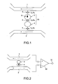
- Fig. 1 is a conceptual diagram of a random number generating device according to the first embodiment of the present invention.
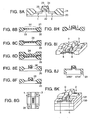
- Fig. 2 is another conceptual diagram of a random number generating device according to the first embodiment of the present invention.
- Fig. 3 shows the potential of a pair of quantum dots.
- Fig. 4 shows that an odd number pairs of quantum dots each having a first nanoparticle 3 and a second nanoparticle 4 are arranged between a first current path 1 and a second current path 2.
- Figs. 5A to 5C show a random number generating device according to the second embodiment of the present invention.
- Fig. 5A is a section view;
- Fig. 5B is a section view; and
- Fig. 5C is a perspective view.
- Figs. 6A and 6B show the structure of a random number generating device according to the third embodiment of the present invention.
- Fig. 7 is a section view of a random number generating device according to the fourth embodiment of the present invention.
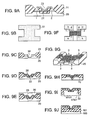
- Figs. 8A to 8K show the random number generating device according to the first example of the present invention.
- Fig. 8A is a section view
- Figs. 8B to 8F and 8H are section views showing the main fabricating steps
- Fig. 8G are a top view
- Fig. 8I is a perspective view
- Fig. 8J is a section view of a modification
- Fig. 8K is a perspective view of the modification.
- Figs. 9A to 9J show the random number generating device according to the second example of the present invention.
- Fig. 9A is a section view;
- Figs. 9C to 9E are section views showing the main fabricating steps;
- Figs. 9B and 9F are top views;
- Fig. 9G is a perspective view;
- Figs. 9H to 9J are section views of a modification.
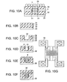
- Figs. 10A to 10G show the random number generating device according to the third example of the present invention.
- Fig. 10A is a section view;
- Figs. 10B to 10F are section views showing the main fabricating steps;
- Fig. 10G is a top view.
- Fig. 11 is a section view of a random number generating device according to the fourth example of the present invention.
- Fig. 12 is a section view of a random number generating device according to the fifth example of the present invention.
- Fig. 13 is a section view of a random number generating device according to the sixth example of the present invention.
- Fig. 14 is a section view of a random number generating device according to the seventh example of the present invention.
- Fig. 15 is a section view of a random number generating device according to the eighth example of the present invention.
- Figs. 16A to 16C are section views of random number generating devices according to other examples of the present invention.
- Fig. 1 is a conceptual view of a random number generating device according to the first embodiment of the present invention.
- the random number generating device includes a pair of first current path 1 and second current path 2, which are placed in parallel with each other, and a pair of first nanoparticle 3 and second nanoparticle 4, which are capable of exchanging electric charges, and are located between the first current path 1 and the second current path 2.
- the size of the first nanoparticle 3 and the second nanoparticle 4 is sufficiently small to enjoy the effects of the wave function of charges.
- the diameter of the nanoparticles is 100 nm or less.
- Such nanoparticles are called "quantum dots.” In a quantum dot, the energy level including charging energy of a charge is discrete.
- first nanoparticle 3 and the second nanoparticle 4 are electrically coupled via a tunnel barrier 6 having a capacitance of C B and a resistance of R B , end charges can be transferred between them.
- first nanoparticle 3 and the first current path 1 are electrically coupled via a barrier 5 having a capacitance of C A and a resistance of R A ; and the second nanoparticle 4 and the second current path 2 are electrically coupled via a barrier 7 having a capacitance of C c and a resistance of R c .
- a pair of quantum dots 23, which is formed by coupling the first nanoparticle 3 and the second nanoparticle 4, is locally not within the conditions of electrical neutrality. That is, it is assumed that an extra charge 8 is injected into the pair of quantum dots 23 from the first current path 1 or the second current path 2, or that the pair of quantum dots 23 is polarized.
- This state can be achieved if the formulas R A >> R B and R c >> R B hold, and charges are transferred more easily within the pair of quantum dots 23, i.e., between the first nanoparticle 3 and the second nanoparticle 4, than between the current paths and the pair of quantum dots 23.
- This random number generating device is achieved based on the fact that when the diameters of the first nanoparticle 3 and the second nanoparticle 4 are on the order of nanometers, the probability that a charge such as an electron exists within the first nanoparticle 3 or the second nanoparticle 4 varies with the physical uncertainty.
- a physical random number can be generated by observing the effect of the charge distribution, which shifts with the physical uncertainty, on the currents flowing through the first current path 1 and the second current path 2.
- the capacitance of a miniaturized structure is C ⁇ ⁇ o S/d, where S is the maximum section area of the miniaturized structure viewed from a direction parallel to the two current paths, d is the minimum length between two structures (quantum dots), and ⁇ 0 is the dielectric constant.
- the capacitance is about 2.2 aF (10 -18 F).
- the charging energy per electron is about 36 meV.
- the charging energy per electron of 36 meV is sufficiently higher than the thermal fluctuation energy of 25.8 meV at the room temperature of 300 K. Accordingly, in the pair of quantum dots 23, the changes in charge distrubution can be observed at the room temperature. This phenomenon is generally called "Coulomb Blockade.”
- time ⁇ t d in which a charge is stabilized in a localized level is estimated to be ⁇ t d ⁇ 1/(C•R).
- ⁇ t d is about 4.5 x 10 -11 seconds.
- the resistance R with which the Coulomb blockade effect can be observed is estimated to be 25.8 k ⁇ or more, and the capacitance C is estimated to be 2.2 aF.
- a current flows through, e.g., the first current path 1
- the charge distribution within the first nanoparticle 3 changes due to the Coulomb repulsion from the electrons of the current flowing through the first current path 1, so that an electron 8 is rearranged so as to go away from the current flowing through the first current path 1.
- the current path is a source-drain path between a silicon FET.
- the mobility between the source and the drain is ⁇
- the electric field applied between the source and the drain is E
- the mobility ⁇ is 1000 cm 2 /(Vs)
- the electric filed E is 10 6 cm/s
- the velocity of electron is 10 15 nm/s. Accordingly, if the diameter of the first nanoparticle 3 is 10 nm, time ⁇ t I in which an electron passes in the vicinity of the first nanoparticle 3 is 10 -13 seconds, and there is a strong interaction between the charge distribution within the first nanoparticle 3 and the current flowing through the first current path 1.
- the charge distribution within the first nanoparticle 3 fluctuates due to the current flowing through the first current path 1, and the fluctuations in charge distribution is reflected back in the current flowing through the first current path 1, so that the current temporally fluctuates.
- the second current path 2 is located in the vicinity of the second nanoparticle 4 and the values of the currents flowing through the first current path 1 and the second current path 2 are adjusted to be substantially on the same order.
- the first current path 1 and the second current path 2 are designed so as to be formed of the same material, and to have substantially the same section area, and the same voltage is applied to both of them.
- the state of charge within the pair of quantum dots 23, i.e., within the first nanoparticle 3 and the second nanoparticle 4 varies depending on the situations, each time it is measured, the difference between the currents flowing through the first current path and the second current path is uniformly distributed in the plus or minus region near zero.
- Fig. 2 shows, in a simplified manner, the differential amplifier 90, which amplifies the difference between the current flowing through the first current path 1 and the current flowing through the second current path 2, and outputs the result from an output terminal 91.
- changes in quantum wave function has a strong influence.
- random numbers generated by the random number generating device are physical random numbers using quantum fluctuations, which are not predictable in a quantum manner. Therefore, even if the number of the pairs of nanoparticles increases, no periodicity appears.
- Fig. 3 schematically shows the potential of the quantum dot pair 23.
- the movement of charges in the quantum dot pair 23 is expressed by the Schroedinger equation (T. Tanamoto, Physical Review A Vol. 61, p022305 (2000)).
- the two quantum dots the first nanoparticle 3 and the second nanoparticle 4
- a charge exists cannot be predicted with certainty by the observation using the first current path 1 or the second current path 2 placed nearby.
- each quantum dot is not necessarily in the ground level, but it is possible to be in an excitation state due to the thermal effect.
- Fig. 4 shows that an odd number pairs of quantum dots 23 each having a first nanoparticle 3 and a second nanoparticle 4 are arranged between the first current path 1 and the second current path 2.
- the probabilities of the appearance of the "0" current and the "1" current are about the same in average.
- the first current path 1 and the second current path 2 has the effect of either "0" or "1" current without fail.
- the Coulomb force acts thereon so that the distribution of charge is opposite in the adjacent two quantum dot pairs 23. Accordingly, it is possible to further inhibit the deviation of distribution in one direction in the quantum dots.
- the random number generating device in this embodiment can function since it has a plurality of quantum dot pairs.
- the effect of the interaction between the temporal changes in potential distribution of a capacitance network, the charge state of which is not stable, and the temporal fluctuations in current is mainly used.
- the random number generating device includes a pair of first current path 1 and second current path 2 arranged in parallel with each other, a microparticle 9 which has a diameter of 1 ⁇ m or less and is located between the first current path 1 and the second current path 2, a first insulating layer 10 located between the microparticle 9 and the first current path 1, and a second insulating layer 11 located between the microparticle 9 and the second current path 2.
- At least one of a first capacitance constituted by the first current path 1, the first insulating layer 10, and the microparticle 9, and a second capacitance constituted by the second current path 2, the second insulating layer 11, and the microparticle 9 is 1 nF or less.
- Fig. 5B shows that there are a plurality of microparticles 9 between the first current path 1 and the second current path 2.
- the Coulomb interaction acts between charges existing in the first current path 1 and the second current path 2 and charges existing in the microparticles 9. Due to the Coulomb interaction, the currents flowing through the first current path 1 and the second current path 2 and the charge distribution within the microparticles 9 temporally fluctuate.
- the Coulomb interaction acting between charges of the microparticles 9 also causes temporal fluctuations of the currents flowing through the first current path 1 and the second current path 2 and the charge distribution within the microparticles 9.
- the number of the insulating layers between the first current path 1 and the second current path 2 can be one, or three or more.
- Fig. 5C shows the case where air is used as an insulating layer between the first and second current paths and the microparticles 9.
- the current flowing through either the first current path 1 from a first source to a first drain or the second current path 2 from a second source to a second drain changes the charge distributions of the microparticles 9, thereby exerting an influence on the other current path. If the current flowing through one current path increases, the current flowing through the other current path is inhibited due to the Coulomb repulsion. Since this phenomenon may temporally change due to thermal fluctuations, etc., it is possible to obtain high-quality random numbers if the fluctuations are outputted as "0"s and "1"s.
- the intervals of quantum energy levels of the microparticles used in the random number generating device according to this embodiment should not necessarily be observed at a predetermined temperature.
- the fluctuations in current paths are caused by the temporal fluctuations of the location of minority charges due to the interactions among the minority charges or between the minority charges and the current paths.
- the degree of the fluctuations of the charges is estimated on the order of the magnitude of charge energy of the capacitor. Accordingly, the less the capacitance of some portions in the microparticles 70 is, the greater the effect obtained is.
- the effect of the strong interaction between the current paths and the charges in the material placed between the current paths to fluctuate the current values is used in the case where there is not a big difference between the plasma frequency inherent to the material placed between the current paths and the degree of temporal fluctuations of currents.
- Fig. 6A shows the structure of a random number generating device according to this embodiment.
- the structure 13 there is a structure 13 between the first current path 1 and the second current path 2.
- the structure 13 is either charged or polarized, and the cycle of the plasma oscillation is about the same as time ⁇ t I (the above-described formula) in which an electron in the currents flowing through the first current path 1 and the second current path 2 pass by a region corresponding to the charge distribution in the structure 13. In this manner, there is a strong interaction between the fluctuations of the charges in the structure 13 and the fluctuations of the electrons flowing through the current paths 1 and 2.
- Fig. 6A shows that plasma oscillation occurs in the structure 13 between the first current path 1 and the second current path 2 of the random number generating device of this embodiment.
- the structure 13 includes microparticles having a diameter of about 1 ⁇ m or less covered by an insulating layer 12.
- nanoparticles 14 having a diameter of about 100 nm or less are located near the first current path 1 and the second current path 2 and electrically connected with each other by a wiring 15.
- the wiring 15 is electrically connected with each nanoparticle 14 via an insulating layer 73.
- the plasma frequency of the wiring 15 is not significantly different from the frequency of the fluctuations in the first current path 1 and the second current path 2, a correlation between the first current path 1 and the second current path 2 occurs, which can be effectively used for generating random numbers.
- the trap levels can be generated by injecting Ga, B, Si, W, etc., into an insulating layer by the use of FIB (Focused Ion Beam).
- Figs. 8A to 16C show that the random number generating devices of the first to the fourth embodiments of the present invention are formed on a silicon substrate. If the size of particles is sufficiently small to cause the quantum effect, the effect explained in the descriptions of the first embodiment can be achieved.
- Fig. 8A shows the section view of the random number generating device according to the first example. A current flows in the direction perpendicular to the sheet of paper.
- an insulating layer 22 is formed on a silicon substrate 20.
- Silicon nanoparticles 23 are formed on the insulating layer 22.
- the silicon nanoparticles 23 are covered by an oxide layer 24.
- two sidewall fine lines 25 are formed.
- the two sidewall fine lines 25 serve as the first current path 1 and the second current path 2.
- the silicon nanoparticles 23 are located between the two sidewall fine lines 25. Charges can transfer from/to the two silicon nanoparticles 23, which constitute the pair of quantum dots 23.
- the method of fabricating this device is as follows.
- device isolation regions 21 are formed on the silicon substrate 20 to form a device region 51. Then, thermal oxidation of the surface of the silicon substrate 20 is performed to form the silicon oxide layer 22 having a thickness of 10 nm or less.
- the silicon substrate 20 may be of either n-type or p-type.
- silicon quantum dots 28 are formed by first forming a polysilicon layer through CVD, etc., and then annealing the polysilicon layer.
- the oxide layer 24 having a thickness of about 8 nm is formed through CVD, etc.
- the oxide layer 24 is patterned by the use of an exposing apparatus. It is preferable that after the patterning, the remaining portion includes one or more silicon quantum dots 28.
- a polysilicon layer is formed through CVD, etc., and the sidewall fine lines 25 are formed at both the sides of the portion containing the silicon quantum dots 28 by removing the polysilicon layer.
- Fig. 8G illustrates the device region viewed from the top of the substrate.
- ion implantation is performed to form the sources (S) and the drains (D) serving as contact regions for the currents.
- the silicon substrate 20 is of n-type, boron, etc. is used, and if the silicon substrate 20 is of p-type, phosphorus etc., is used.
- Fig. 8I is a perspective view of Fig. 8H.
- the sidewall fine lines 25 serve as the first current path 1 and the second current path 2 used to detect the effect of the charge distribution of the adjacent quantum dots.
- Nanoparticles such as polystyrene beads can be used as the quantum dots 28. Further, metal fine particles such as Au can also be used.
- an amorphous silicon layer can be used instead of the quantum dots 28, since there are many trap levels in amorphous silicon, it can be used as a substitute for the pair of quantum dots 23.
- Fig. 8J is a section view in the case where STI (Shallow Trench Isolation) 27 is used for isolating devices.
- STI Shallow Trench Isolation
- Fig. 8K is a perspective view in which an SOI substrate 100 is used instead of the substrate 200.
- the portion into which ions are injected can reach the oxide layer 101 in the substrate.
- Fig. 9A is a section view of the random number generating device according to the second example. Currents flow in the direction perpendicular to the paper plane.
- an insulating layer 22 is formed on a silicon substrate 20. Silicon microparticles 23 are formed on the insulating layer 22. Under the insulating layer 22 on the silicon substrate 20, the first current path 1 and the second current path 2 are formed. The silicon microparticles 23 are arranged between the first current path 1 and the second current path 2.
- the method of fabricating this device is as follows.
- a device region 51 is formed on the silicon substrate 20 so as to have recessed portions.
- Fig. 9B is a top view.
- the recessed portions are not indispensable, since they are for effectively detecting the changes in electric field of the quantum dots.
- a conduction region is formed by injecting ions to the device region 51.
- the types of ions to be injected are the same as those for the first example.
- a trench 30 is formed by exposing the center portion of the device region by the use of an electron beam exposing apparatus, and etching the silicon substrate 20.
- Fig. 9G is a perspective view of the device in Fig. 9D.
- Fig. 9F is a top view of the device in Fig. 9D.
- an oxide layer 80 is deposited through CVD, etc., and a contact hole is formed to form a current terminal.
- the circled portion has an effect of quantum dot pairs 23.
- quantum dots of a material other than polysilicon can also be used.
- the trench 30 can be formed by anisotropic etching utilizing, e.g., the plane direction of the silicon substrate 20.
- Fig. 9I is a section view in which STIs 27 are used for isolating devices.
- Fig. 9J is a section view in which an SOI substrate 100 is used.
- the portion into which ions are injected can reach the oxide layer 101 in the substrate.
- Fig. 10A is a section view of the random number generating device according to the third example. Currents flow in the direction perpendicular to the paper plane.
- silicon nanoparticles 9 are filled in a trench, and the first current path 1 and the second current path 2 are formed at both sides of the trench via an insulating layer 31.
- the first current path 1 and the second current path 2 are formed on a silicon oxide layer 32.
- a pair of silicon nanoparticles 9 constitutes the coupled quantum dots 23.
- the method of fabricating this device is as follows.
- a silicon oxide layer 32 having a thickness of a few hundreds nm or more is formed on a silicon substrate 20.
- a polysilicon layer 33 is formed on the silicon oxide layer 32.
- the polysilicon layer 33 will serve as the first current path and the second current path later.
- a silicon oxide layer 34 is formed on the polysilicon layer 33 through CVD, etc.
- part of the silicon oxide layer 34, the polysilicon layer 33, and the silicon oxide layer 32 is patterned to form a trench 30.
- a thin oxide layer 31 is formed on the inner sidewall of the trench 30 through thermal oxidation.
- silicon quantum dots 9 are formed of polysilicon, etc., in the trench 30.
- a protection oxide layer 35 is formed through CVD, etc.
- Fig. 10G is a top view of the device.
- Fig. 11 is a section view of the random number generating device according to the fourth example. Currents flow in the direction perpendicular to the paper plane.
- the second current path 2 is formed on an insulating layer 40.
- the first current path 1 is formed on the second current path 2 via an insulating layer 41.
- An insulating layer 42 is formed on the first current path 1.
- the first current path 1 and the second current path 2 have end portions formed by etching, at which a sidewall insulating layer 43 is formed. Silicon fine particles 9 are formed on the sidewall of the sidewall insulating layer 43. These silicon fine particles constitute quantum dots 23.
- the above-described structure can be achieved by patterning part of laminated layers formed by laminating the insulating layer 40, the second current path 2, the insulating layer 41, and the first current path 1, oxidizing the angled portion, and depositing the silicon fine particles 23 on the angled portion.
- Fig. 12 is a section view of a random number generating device according to the fifth example.
- the second current path 2 is formed on a silicon thermal oxide layer 40 obtained by heating the substrate. Pairs of quantum dots 23 are formed on the second current path 2 by embedding silicon fine particles 9 in a silicon oxide layer 45 formed through CVD.
- the first current path 1 is formed on the pairs of quantum dots 23.
- a silicon oxide layer 42 is formed on the first current path 1 through CVD.
- This structure can be achieved by laminating the silicon thermal oxide layer 40, the second current path 2, the pairs of quantum dots 23 obtained by embedding silicon fine particles 9 in the silicon oxide layer 45, the first current path 1, and the silicon oxide layer 42, and performing patterning thereof.
- Fig. 13 is a section view of a random number generating device according to the sixth example.
- the second current path 2 is formed on a silicon thermal oxide layer 50 obtained by heating a substrate.
- a silicon oxide layer 51 is formed on the second current path 2 through CVD.
- a silicon nitride layer 52 is formed on the silicon oxide layer 51.
- a silicon oxide layer 53 is formed on the silicon nitride layer 52 through CVD.
- the first current path 1 is formed on the silicon oxide layer 53.
- a silicon oxide layer 54 is formed on the first current path 1 through CVD.
- trap levels 55 are formed at the interfaces between the silicon nitride layer 52 and the silicon oxide layer 51, and between the silicon nitride layer 52 and the silicon oxide layer 53. The trap levels are formed between the first current path 1 and the second current path 2.
- Fig. 14 is a section view of a random number generating device according to the seventh example.
- the second current path is formed on a silicon thermal oxide layer 50 obtained by hearing a substrate.
- a silicon oxide layer 51 is formed on the second current path 2 through CVD.
- An amorphous silicon layer 60 is formed on the silicon oxide layer 51.
- a silicon oxide layer 53 is formed on the amorphous silicon layer 60 through CVD.
- the first current path 1 is formed on the silicon oxide layer 53.
- a silicon oxide layer 54 is formed on the first current path 1 thorough CVD.
- the amorphous silicon layer 60 has grain boundaries, part of which serves as quantum dots. Further, since trap levels exist at grain boundaries of the amorphous silicon layer 60, the trap levels can be used.
- Fig. 15 is a section view of a random number generating device according to the eighth example.
- pairs of quantum dots 23 covered by a thermal oxide layer are formed on a silicon substrate 20.
- a silicon layer 61 is formed thereon.
- the surface of the silicon substrate 20 serves as the second current path 2.
- the silicon layer 61 serves as the first current path.
- This structure can be achieved by laminating silicon on a silicon thermal oxide layer obtained by heating the substrate with the epitaxila technique, and then crystallizing it to form the first current path 1.
- a gate electrode 62 is formed thereon. The gate electrode 62 is used to adjust the current amount of the first current path 1 and the second current path 2.
- the quantum dots in the first, second, and fourth examples are replaced by trap levels 55 formed by injecting ions of Ga, B, Si, W, and the like by Focused Ion Beam (FIB).
- FIB Focused Ion Beam
- the trap levels may reach the substrate. Further, it is possible to form trap levels between the silicon substrate and the thermal oxide layer by roughening the surface of the silicon substrate by using KOH or the like without using FIB.
- the first current path and the second current path are formed of polysilicon.
- a silicide material such as CoSi, FeSi, NiSi, TiSi, etc. can be used in order to improve the conductivity.
- the first current path and the second current path can be formed of a metal such as Al, Fe, Ti, Ni, Co, and Cu.
- quantum dots of the above-described examples
- silicidation of the surface of the quantum dots can be performed.
- two types of semiconductors or metals can be used to form the quantum dots.
- the gate electrode on the device or on the backside of the substrate so as to adjust the charge distribution of the quantum dots.
- a magnetic field can be applied to the device.
- the quantum dots can be placed in a cavity or a multiple quantum well structure.
- pairs of coupled quantum dots are mainly used.
- the number of quantum dots coupled can be three or more.
- the number of laminated quantum dots can be three or more.
- the device isolation can be performed by Local Oxidation of Silicon (LOCOS), Shallow Trench Isolation (STI), or other methods.
- LOCOS Local Oxidation of Silicon
- STI Shallow Trench Isolation
- a silicon oxide layer is used as a tunnel oxide layer or an insulating layer in the above-described embodiments
- a high dielectric constant material such as SiN, alumina, HfO 2 , ZrO 2 , etc. can be used instead. Further, two or more of these materials can be laminated.
- the first current path and the second current path may have constricted portions, i.e., so-called the point contact structure. Or, they may be single electron devices.
- the substrate is a silicon substrate in the above embodiments, it may be formed of glass, STO, GaN, GaAs, etc.
- quantum fluctuations or thermal fluctuations of subtle charges have influence on currents flowing through current paths. Accordingly, it is possible to generate high-quality random numbers at a high speed and without a deviation by using the difference in the currents flowing through the currents paths as random number data.
Landscapes
- Engineering & Computer Science (AREA)
- Theoretical Computer Science (AREA)
- Physics & Mathematics (AREA)
- Nanotechnology (AREA)
- General Physics & Mathematics (AREA)
- Chemical & Material Sciences (AREA)
- Pure & Applied Mathematics (AREA)
- Computer Security & Cryptography (AREA)
- Mathematical Optimization (AREA)
- Mathematical Physics (AREA)
- Mathematical Analysis (AREA)
- Crystallography & Structural Chemistry (AREA)
- Computational Mathematics (AREA)
- General Engineering & Computer Science (AREA)
- Computer Networks & Wireless Communication (AREA)
- Signal Processing (AREA)
- Semiconductor Integrated Circuits (AREA)
- Light Receiving Elements (AREA)
- Thin Film Transistor (AREA)
- Non-Volatile Memory (AREA)
- Control Of Electrical Variables (AREA)
Applications Claiming Priority (2)
| Application Number | Priority Date | Filing Date | Title |
|---|---|---|---|
| JP2002054153A JP3974429B2 (ja) | 2002-02-28 | 2002-02-28 | 乱数発生素子 |
| JP2002054153 | 2002-02-28 |
Publications (2)
| Publication Number | Publication Date |
|---|---|
| EP1341079A2 true EP1341079A2 (de) | 2003-09-03 |
| EP1341079A3 EP1341079A3 (de) | 2006-03-01 |
Family
ID=27678564
Family Applications (1)
| Application Number | Title | Priority Date | Filing Date |
|---|---|---|---|
| EP03251249A Withdrawn EP1341079A3 (de) | 2002-02-28 | 2003-02-28 | Zufallszahlengenerator |
Country Status (3)
| Country | Link |
|---|---|
| US (4) | US7405423B2 (de) |
| EP (1) | EP1341079A3 (de) |
| JP (1) | JP3974429B2 (de) |
Cited By (2)
| Publication number | Priority date | Publication date | Assignee | Title |
|---|---|---|---|---|
| WO2005085992A1 (de) * | 2004-03-08 | 2005-09-15 | Siemens Aktiengesellschaft | Manipulationssichere erzeugung von echten zufallszahlen |
| EP2421043A1 (de) * | 2010-08-20 | 2012-02-22 | Hitachi, Ltd. | Quantenpunktvorrichtung |
Families Citing this family (28)
| Publication number | Priority date | Publication date | Assignee | Title |
|---|---|---|---|---|
| JP3974429B2 (ja) * | 2002-02-28 | 2007-09-12 | 株式会社東芝 | 乱数発生素子 |
| US7589029B2 (en) | 2002-05-02 | 2009-09-15 | Micron Technology, Inc. | Atomic layer deposition and conversion |
| JP4359130B2 (ja) * | 2003-12-05 | 2009-11-04 | 株式会社東芝 | 乱数生成素子 |
| DE602006013409D1 (de) * | 2005-01-17 | 2010-05-20 | Biophos Ag | Verfahren und vorrichtung zur messung dynamischer partikelparameter |
| WO2007011660A2 (en) * | 2005-07-14 | 2007-01-25 | William Marsh Rice University | Quantum dot probes |
| US7927948B2 (en) | 2005-07-20 | 2011-04-19 | Micron Technology, Inc. | Devices with nanocrystals and methods of formation |
| US7989290B2 (en) | 2005-08-04 | 2011-08-02 | Micron Technology, Inc. | Methods for forming rhodium-based charge traps and apparatus including rhodium-based charge traps |
| US7575978B2 (en) | 2005-08-04 | 2009-08-18 | Micron Technology, Inc. | Method for making conductive nanoparticle charge storage element |
| JP4160605B2 (ja) * | 2006-05-09 | 2008-10-01 | 株式会社東芝 | 乱数発生装置 |
| JP2009544024A (ja) * | 2006-07-17 | 2009-12-10 | ビオフォス アクチエンゲゼルシャフト | 画像相関によるモバイル粒子分析装置 |
| WO2008087692A1 (ja) * | 2007-01-19 | 2008-07-24 | Hiroshima University | 半導体メモリ、それを用いた半導体メモリシステム、および半導体メモリに用いられる量子ドットの製造方法 |
| JP4594971B2 (ja) | 2007-01-19 | 2010-12-08 | 国立大学法人広島大学 | 半導体メモリ、それを用いた半導体メモリシステム、および半導体メモリに用いられる量子ドットの製造方法 |
| JP2008288346A (ja) | 2007-05-16 | 2008-11-27 | Hiroshima Univ | 半導体素子 |
| US8367506B2 (en) | 2007-06-04 | 2013-02-05 | Micron Technology, Inc. | High-k dielectrics with gold nano-particles |
| JP5128355B2 (ja) * | 2008-04-18 | 2013-01-23 | 日本電信電話株式会社 | 乱数発生素子 |
| JP5295651B2 (ja) * | 2008-06-13 | 2013-09-18 | 株式会社東芝 | 乱数生成装置 |
| US8495118B2 (en) * | 2008-10-30 | 2013-07-23 | Seagate Technology Llc | Tunable random bit generator with magnetic tunnel junction |
| JP4368934B1 (ja) | 2009-02-09 | 2009-11-18 | アイランド ジャイアント デベロップメント エルエルピー | 液体収容システム、液体収容容器、および液体導出制御方法 |
| US9013784B2 (en) * | 2010-10-29 | 2015-04-21 | Hewlett-Packard Development Company, L.P. | Nanoparticle waveguide apparatus, system and method |
| WO2012158791A2 (en) * | 2011-05-16 | 2012-11-22 | The Board Of Trustees Of The University Of Illinois | Electronic device from dissipative quantum dots |
| CN105144388A (zh) * | 2013-03-09 | 2015-12-09 | 国立研究开发法人科学技术振兴机构 | 逻辑计算元件 |
| WO2015033600A1 (ja) * | 2013-09-06 | 2015-03-12 | 独立行政法人科学技術振興機構 | 電極対、その作製方法、デバイス用基板及びデバイス |
| CA2948408C (en) * | 2014-05-09 | 2023-03-07 | Quantum Numbers Corp. | Method for generating random numbers and associated random number generator |
| ES2910453T3 (es) * | 2014-06-06 | 2022-05-12 | Newsouth Innovations Pty Ltd | Aparato de procesamiento avanzado |
| GB2543125B (en) * | 2016-07-27 | 2017-10-18 | Quantum Base Ltd | Generating a unique response to a challenge |
| US10168996B1 (en) | 2018-01-15 | 2019-01-01 | Quantum Numbers Corp. | Method and system for generating a random bit sample |
| CN108776582B (zh) * | 2018-05-08 | 2021-09-21 | 清华大学 | 一种基于量子隧穿效应的真随机数序列产生方法 |
| US20240008299A1 (en) * | 2020-12-25 | 2024-01-04 | Sharp Kabushiki Kaisha | Light-emitting element |
Family Cites Families (11)
| Publication number | Priority date | Publication date | Assignee | Title |
|---|---|---|---|---|
| US5377129A (en) * | 1990-07-12 | 1994-12-27 | Massachusetts Institute Of Technology | Particle interaction processing system |
| DE69721929T2 (de) * | 1996-03-26 | 2004-05-13 | Samsung Electronics Co., Ltd., Suwon | Tunneleffektanordnung und verfahren zur herstellung |
| AT405109B (de) * | 1997-05-21 | 1999-05-25 | Wasshuber Christoph Dipl Ing D | Ein-elektron speicherbauelement |
| TW381057B (en) * | 1997-08-07 | 2000-02-01 | Hitachi Ltd | Semiconductor device |
| US7015499B1 (en) * | 1999-12-01 | 2006-03-21 | D-Wave Systems, Inc. | Permanent readout superconducting qubit |
| JP4873335B2 (ja) * | 2000-04-28 | 2012-02-08 | 独立行政法人科学技術振興機構 | 情報処理構造体 |
| US6492843B1 (en) * | 2000-09-29 | 2002-12-10 | Intel Corporation | Random frequency clock generator |
| KR100455282B1 (ko) * | 2001-01-11 | 2004-11-08 | 삼성전자주식회사 | 램 및 롬 기능을 갖는 단일 트랜지스터를 포함하는 메모리소자와 그 동작 및 제조방법 |
| KR100459895B1 (ko) * | 2002-02-09 | 2004-12-04 | 삼성전자주식회사 | 퀀텀 도트를 가지는 메모리 소자 및 그 제조방법 |
| JP3974429B2 (ja) * | 2002-02-28 | 2007-09-12 | 株式会社東芝 | 乱数発生素子 |
| US7105425B1 (en) * | 2002-05-16 | 2006-09-12 | Advanced Micro Devices, Inc. | Single electron devices formed by laser thermal annealing |
-
2002
- 2002-02-28 JP JP2002054153A patent/JP3974429B2/ja not_active Expired - Fee Related
-
2003
- 2003-02-27 US US10/373,874 patent/US7405423B2/en not_active Expired - Fee Related
- 2003-02-28 EP EP03251249A patent/EP1341079A3/de not_active Withdrawn
-
2008
- 2008-06-20 US US12/143,104 patent/US7558813B2/en not_active Expired - Fee Related
- 2008-06-20 US US12/143,206 patent/US8330160B2/en not_active Expired - Fee Related
- 2008-06-20 US US12/143,124 patent/US7629609B2/en not_active Expired - Fee Related
Non-Patent Citations (1)
| Title |
|---|
| PHYS. REV. A, vol. 61, 2000, pages 022305-1 - 022305-7 |
Cited By (3)
| Publication number | Priority date | Publication date | Assignee | Title |
|---|---|---|---|---|
| WO2005085992A1 (de) * | 2004-03-08 | 2005-09-15 | Siemens Aktiengesellschaft | Manipulationssichere erzeugung von echten zufallszahlen |
| US7496617B2 (en) | 2004-03-08 | 2009-02-24 | Siemens Aktiengesellschaft | Tamper proof generation of true random numbers |
| EP2421043A1 (de) * | 2010-08-20 | 2012-02-22 | Hitachi, Ltd. | Quantenpunktvorrichtung |
Also Published As
| Publication number | Publication date |
|---|---|
| JP3974429B2 (ja) | 2007-09-12 |
| EP1341079A3 (de) | 2006-03-01 |
| JP2003258240A (ja) | 2003-09-12 |
| US20080256152A1 (en) | 2008-10-16 |
| US7558813B2 (en) | 2009-07-07 |
| US20030162587A1 (en) | 2003-08-28 |
| US20080251783A1 (en) | 2008-10-16 |
| US7405423B2 (en) | 2008-07-29 |
| US7629609B2 (en) | 2009-12-08 |
| US8330160B2 (en) | 2012-12-11 |
| US20080251782A1 (en) | 2008-10-16 |
Similar Documents
| Publication | Publication Date | Title |
|---|---|---|
| US7629609B2 (en) | Random number generating device | |
| KR100372668B1 (ko) | 반도체 장치 | |
| US6716690B1 (en) | Uniformly doped source/drain junction in a double-gate MOSFET | |
| US20040063289A1 (en) | Reduction in source-drain resistance of semiconductor device | |
| US7494862B2 (en) | Methods for uniform doping of non-planar transistor structures | |
| TW405225B (en) | Semiconductor device and manufacturing method therefor | |
| US8686514B2 (en) | Multiple threshold voltages in field effect transistor devices | |
| CN103377999B (zh) | 具有连接通孔结构的3维集成电路系统及用以形成该集成电路系统的方法 | |
| EP2421043B1 (de) | Quantenpunktvorrichtung | |
| US20200343435A1 (en) | Method for producing an electronic component with double quantum dots | |
| JP3743745B2 (ja) | 半導体素子 | |
| Batra et al. | Detection of low energy single ion impacts in micron scale transistors at room temperature | |
| JP5841013B2 (ja) | 半導体装置 | |
| WO2011019913A1 (en) | Silicon photon detector | |
| US7217620B2 (en) | Methods of forming silicon quantum dots and methods of fabricating semiconductor memory device using the same | |
| KR100966008B1 (ko) | 상온동작 단전자 소자 및 그 제조방법 | |
| US7605045B2 (en) | Field effect transistors and methods for fabricating the same | |
| US20080116522A1 (en) | Cmos structure including topographic active region | |
| JPH09191104A (ja) | 単一電子素子 | |
| US8652963B2 (en) | MOSFET integrated circuit with uniformly thin silicide layer and methods for its manufacture | |
| CN107017166A (zh) | 控制eDRAM深沟槽上方的外延生长以及如此形成的eDRAM | |
| US10950726B2 (en) | Semiconductor device, CMOS circuit, and electronic apparatus with stress in channel region | |
| KR101012265B1 (ko) | 상온동작 단전자 소자의 제작방법 | |
| JPH11195780A (ja) | 単一電子装置およびその製造方法 | |
| WO2006068107A1 (ja) | 電荷蓄積増倍装置及びそれを用いたイメージセンサ |
Legal Events
| Date | Code | Title | Description |
|---|---|---|---|
| PUAI | Public reference made under article 153(3) epc to a published international application that has entered the european phase |
Free format text: ORIGINAL CODE: 0009012 |
|
| 17P | Request for examination filed |
Effective date: 20030310 |
|
| AK | Designated contracting states |
Kind code of ref document: A2 Designated state(s): AT BE BG CH CY CZ DE DK EE ES FI FR GB GR HU IE IT LI LU MC NL PT SE SI SK TR |
|
| AX | Request for extension of the european patent |
Extension state: AL LT LV MK RO |
|
| PUAL | Search report despatched |
Free format text: ORIGINAL CODE: 0009013 |
|
| RIC1 | Information provided on ipc code assigned before grant |
Ipc: H01L 29/788 20060101ALI20060104BHEP Ipc: H03K 3/84 20060101ALI20060104BHEP Ipc: G06F 7/58 20060101AFI20030531BHEP |
|
| AK | Designated contracting states |
Kind code of ref document: A3 Designated state(s): AT BE BG CH CY CZ DE DK EE ES FI FR GB GR HU IE IT LI LU MC NL PT SE SI SK TR |
|
| AX | Request for extension of the european patent |
Extension state: AL LT LV MK RO |
|
| AKX | Designation fees paid |
Designated state(s): DE FR GB |
|
| 17Q | First examination report despatched |
Effective date: 20070509 |
|
| GRAP | Despatch of communication of intention to grant a patent |
Free format text: ORIGINAL CODE: EPIDOSNIGR1 |
|
| STAA | Information on the status of an ep patent application or granted ep patent |
Free format text: STATUS: THE APPLICATION IS DEEMED TO BE WITHDRAWN |
|
| 18D | Application deemed to be withdrawn |
Effective date: 20100320 |