EP1298794A2 - Circuit de réduction de bruit de commutation et amplificateur pour fréquences vocales - Google Patents
Circuit de réduction de bruit de commutation et amplificateur pour fréquences vocales Download PDFInfo
- Publication number
- EP1298794A2 EP1298794A2 EP02021728A EP02021728A EP1298794A2 EP 1298794 A2 EP1298794 A2 EP 1298794A2 EP 02021728 A EP02021728 A EP 02021728A EP 02021728 A EP02021728 A EP 02021728A EP 1298794 A2 EP1298794 A2 EP 1298794A2
- Authority
- EP
- European Patent Office
- Prior art keywords
- power source
- amplifier
- pulse width
- time
- voltage
- Prior art date
- Legal status (The legal status is an assumption and is not a legal conclusion. Google has not performed a legal analysis and makes no representation as to the accuracy of the status listed.)
- Granted
Links
Images
Classifications
-
- H—ELECTRICITY
- H03—ELECTRONIC CIRCUITRY
- H03F—AMPLIFIERS
- H03F3/00—Amplifiers with only discharge tubes or only semiconductor devices as amplifying elements
- H03F3/20—Power amplifiers, e.g. Class B amplifiers, Class C amplifiers
- H03F3/21—Power amplifiers, e.g. Class B amplifiers, Class C amplifiers with semiconductor devices only
- H03F3/217—Class D power amplifiers; Switching amplifiers
-
- H—ELECTRICITY
- H03—ELECTRONIC CIRCUITRY
- H03F—AMPLIFIERS
- H03F1/00—Details of amplifiers with only discharge tubes, only semiconductor devices or only unspecified devices as amplifying elements
- H03F1/30—Modifications of amplifiers to reduce influence of variations of temperature or supply voltage or other physical parameters
- H03F1/305—Modifications of amplifiers to reduce influence of variations of temperature or supply voltage or other physical parameters in case of switching on or off of a power supply
-
- H—ELECTRICITY
- H03—ELECTRONIC CIRCUITRY
- H03G—CONTROL OF AMPLIFICATION
- H03G3/00—Gain control in amplifiers or frequency changers without distortion of the input signal
- H03G3/20—Automatic control
- H03G3/30—Automatic control in amplifiers having semiconductor devices
- H03G3/34—Muting amplifier when no signal is present or when only weak signals are present, or caused by the presence of noise signals, e.g. squelch systems
- H03G3/348—Muting in response to a mechanical action or to power supply variations, e.g. during tuning; Click removal circuits
Definitions
- the present invention relates to a pop sound reduction circuit which is applied to a voice output device constituted by semiconductor integrated circuits, and more particularly to a pop sound reduction circuit which reduces pop sound generated at the time when power is turned on/off and a voice output amplification device comprising the same.
- a power supply from one electric power source has been considered to be advantageous from the viewpoint of a circuit scale and cost.
- a pulse width modulation amplifier performs a switching operation at a constant frequency and a constant duty ratio (usually 50 %) so that an output reference potential during a normal operation becomes equal to a predetermined DC value (usually about VCC/2).
- the output reference potential obtained by the switching operation by the pulse width modulation amplifier at the time when the power source is turned on reaches smoothly from a potential of a GND level to a predetermined output DC potential during the normal operation.
- noises having a frequency of an audio band should not be generated.
- the switching frequency In the vicinity of the lowest operation voltage of the circuit itself, the switching frequency itself passes through the audio band, and thus the switching frequency may generate noises called pop sound.
- the output reference potential decreases smoothly from the value during the normal operation to the GND level when the electric power source is turned off. During this period of time, no generation of noises having an audio frequency band is desired, and it is desirable that the circuit is stopped in a state where unnecessary noises occur after turning-off of the electric power source.
- the voice output amplification device having the SEPP circuit structure using the switching system, to which power is supplied from one electric power source, a countermeasure to improve the level of the pop sound by canceling the voltage variation of GND by making the output a BLT structure and by making the power supplied from two electric power systems.
- the BTL structure is adopted, the number of amplifiers per one channel is doubled, and when the voice output amplification device is powered from two electric power sources, the structure of the power sources become complex. Therefore, the voice output amplification device encounters a problem of high cost.
- a pop sound reduction circuit comprises a pulse width modulation amplifier configured to amplify a reference voltage to an intermediate amplitude of a pulse width modulated signal, a first switch configured to activate and deactivate the pulse width modulation amplifier, a buffer amplifier configured to generate a DC voltage equal to the reference voltage, a second switch configured to activate and deactivate the buffer amplifier, and a control circuit configured to close and open the first and second switches complementary, depending on a potential in a leading region of the reference voltage which rises from a time of turning-on of a power source as well as a potential in a trailing region of the reference voltage which falls from a time of turning-off of the power source.
- a voice output amplification device comprises a pulse width modulation amplifier configured to convert an input signal to a pulse width modulated signal by use of a triangular wave signal, a triangular wave oscillator configured to supply the triangular wave signal to the pulse width modulation amplifier, a reference voltage generator configured to generate a first reference voltage respectively having time constants in a leading region from a time of turning-on of a power source and a trailing region from a time of turning-off of the power source, an input amplifier configured to amplify the input signal to a predetermined potential to supply the amplified input signal to the pulse width modulation amplifier, a pop sound reduction circuit, and a power source line configured to supply a power source voltage, wherein the input signal is converted to the pulse width modulated signal which swings between the power source voltage and a ground potential, and then the pulse width modulated signal is delivered as an analog output signal at an output stage provided outside the voice output amplification device.
- a method for reducing pop sound comprises delivering a leading output voltage from a buffer amplifier by deactivating a pulse width modulation amplifier and activating the buffer amplifier complementary until first and second reference voltages reach a stable region of the pulse width modulation amplifier from a time of turning-on of a power source, delivering an output voltage from the pulse width modulation amplifier by activating the pulse width modulation amplifier and deactivating the buffer amplifier complementary after the first and second output reference voltages reach the stable region of the pulse width modulation amplifier, and delivering a trailing output voltage from the buffer amplifier by deactivating the pulse width modulation amplifier and activating the buffer amplifier complementary from a time just before the first and second reference voltages pass through the stable region from a time of turning-off of the power source.
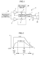
- Fig. 1 is a block diagram for explaining a basic operation of a voice output amplification device comprising a pop sound reduction circuit according to an embodiment.
- Fig. 2 is a voltage waveform diagram for a period of time from a power source on to a power source off in Fig. 1.
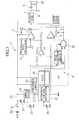
- Fig. 3 is a circuit constitution view of the voice output amplification device comprising the pop sound reduction circuit according to the embodiment.
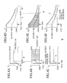
- Figs. 4A to 4F are voltage waveform diagrams for a period of time from the power source on to the power source off.
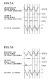
- Figs. 5A and 5B are waveform diagrams illustrating a relation between a triangular waveform signal and an output current appearing at an output stage.
- a voice output amplification device 1 comprises a pulse width modulation amplifier (PWM) 2 which sets a reference voltage to an intermediate potential of an amplitude of a pulse width signal and converts an input signal to a pulse width modulated (PWM) signal by use of a triangular wave signal; a buffer amplifier 3 configured to generate a DC voltage equal to the reference voltage; and a pop sound reduction circuit 30.
- the pop sound reduction circuit 30 comprises a first switch 4 configured to open and close the output path from a PWM amplifier 2; a second switch 5 configured to open and close the output path from the buffer amplifier 3; and a control circuit 6 configured to control the first and second switches 4 and 5 to allow the output from one of the PWM amplifier 2 and the buffer amplifier 3 to be delivered.
- a reference voltage generator circuit 19 is coupled to the voice output amplification device 1 so that the reference voltage, that is defined as a voltage at the intermediate potential during a normal operation, can be supplied to the voice output amplification device 1. Note that other signal inputs and a power source in the respective amplifiers are omitted.
- first and second switches 4, 5 open and close the output paths from the PWM 2 and buffer amplifier 3, the first and second switches can be employed such that the power supplies to the PWM 2 and buffer amplifier 3 are opened and closed.
- the control circuit 6 opens the first switch 4 and closes the second switch 5, thus allowing only the output from the buffer amplifier 3 can be delivered. Since a predetermined time constant is imparted to the reference voltage that is being supplied to the buffer amplifier 3, an output voltage OUTPUT DC from the buffer amplifier 3 rises gradually. Subsequently, when the reference voltage reaches the stable operation voltage region of the PWM amplifier 2, the control circuit 6 closes the first switch 4 and opens the second switch 5, thus the output from the PWM amplifier 2 can be delivered.
- a PWM signal which was converted from the input signal is delivered as an output signal in the PWM amplifier 2.
- This PWM signal is a switching waveform signal which sets the reference voltage to the intermediate amplitude of the PWM signal and alternates between the power source voltage VCC and the ground potential GND. Each pulse is modulated to a time width in accordance with the input signal.
- the output voltage OUTPUT DC is delivered from the buffer amplifier 3 until the reference voltage reaches the stable operation voltage region of the PWM amplifier 2, and the PWM amplifier 2 is operated after the reference voltage reached the stable operation voltage region of the PWM amplifier 2, whereby it is possible to reduce the occurrence of abnormal sound and pop sound due to an unstable operation of the PWM amplifier 2 at the time when the power source VCC is turned on. Furthermore, as described later, by exchanging the output of the amplifier 2, 3 at a timing such that current fluctuation at the output stage of the voice output amplification device 1 becomes minimum, it is possible to further decrease the pop sound.
- the control circuit 6 opens the first switch 4 and closes the second switch 5 before the reference voltage passes through the stable operation voltage region of the PWM 2, thus allowing the delivery of the output from the buffer amplifier 3.
- the output voltage OUTPUT DC from the buffer amplifier 3 gradually decreases, and then becomes equal to the GND level.
- Fig. 3 is another circuit configuration of the voice output amplification device according to the embodiment of the present invention, which shows the SEPP circuit using the above mentioned exchanging system, wherein the power supply to the amplifier 2,3 is exchanged using one electric power source 32.
- the PWM amplifier 2 compares an analog input signal, for example, an audio signal, which is supplied from an input amplifier 16, and a triangular wave signal which is supplied from a triangular wave oscillator 17, and converts the input signal to the PWM signal by the PWM operation, thus outputting the PWM signal.
- the PWM amplifier 2 shown in Fig. 3 is constituted by a PWM comparator and an output circuit amplifier.
- the power source voltage VCC is supplied to the PWM amplifier 2 through a first switch 4.
- the buffer amplifier 3 is a linear amplifier for generating a DC voltage equal to the reference voltage VCC/2.
- the buffer amplifier 3 generates an output voltage equivalent to the reference voltage for a period of time until the output reference voltage reaches the stable operation voltage region of the PWM amplifier 2 after the reference voltage stabilizes at VCC/2 after turning-on of the power source. Also at the time of the turning-off of the power source, the buffer amplifier 3 is activated immediately before the reference voltage passes through the stable operation voltage region of the PWM amplifier 2, and the buffer amplifier 3 outputs the output voltage which gradually falls to the GND level. Moreover, at the time of the turning-off of the power source, the buffer amplifier 3 discharges charges remaining in the output stage to the outside.
- the switching of the first and second switches 4 and 5 are controlled complementarily depending on the output signal from a hysteresis comparator 21. Specifically, when the first switch 4 is closed, the second switch is opened. When the first switch 4 is opened, the second switch 5 is closed.
- the input amplifier 16 amplifies the analog input signal by use of the reference voltage delivered from an reference voltage generator 19.
- the triangular wave oscillator 17 generates the triangular signal, which is compared with the input signal in the PWM amplifier 2.
- the triangular wave signal generated in the triangular wave oscillator is transmitted to the PWM amplifier 2 and a peak detection circuit 18.
- a sawtooth wave signal can be also used.
- the position of the peak voltage and the position where fluctuation of the output current at the output stage becomes minimum do not coincide with each other temporally. Accordingly, the phase of the peak voltage must be corrected.
- a circuit for correcting the phase may be provided at the front stage of the peak detection circuit 18, or the configuration of the voice output amplification device is modified so that the sawtooth signal is supplied only to the PWM amplifier 2, and a triangular wave signal from the triangular wave oscillator 17 in synchronization with the sawtooth signal is supplied to the peak detection circuit 18.
- the peak detection circuit 18 detects a peak voltage of the triangular wave signal generated by the triangular wave oscillator 17, and provides a detection signal to the hysteresis comparator 21 at a timing when the peak voltage is detected.
- the reference voltage generator 19 generates the reference voltage VCC/2 that serve as the operation reference voltages of the PWM amplifier 2 and the buffer amplifier 3.
- the foregoing PWM amplifier 2 sets the reference voltage to the intermediate potential of the amplitude of the PWM signal, and generates the PWM signal which swings between the power source voltage VCC and the ground potential GND.
- the reference voltage delivered from the PWM amplifier 2 has time constants at the leading region spanning from the time of he turning-on the power source and at the trailing region after the time of the turning-off the power source, respectively.
- the reference voltage provided by the PWM amplifier 2 rises to VCC/2 with a predetermined leading time from the time of the turning-on the power source, and decreases from VCC/2 to the GND level with a predetermined breaking time from the time of the turning-off the power source.
- the power source voltage VCC 32 is supplied to the reference voltage generator 19 through a ripple filter 23 via a power source line 33, and the time constant is imparted by a capacitor 26 provided at the outside.
- the reference voltage corresponds to a first reference voltage in this embodiment, and is supplied to the buffer amplifier 3 and the hysteresis comparator 21 through a power source input line (not shown).
- a VCC/2 generator 20 generates a VCC/2 for the output detection to be supplied to the hysteresis comparator 21.
- the VCC/2 for the output detection is an intermediate potential between the power source VCC and the ground potential GND similar to the reference voltage VCC/2, and the VCC/2 for the output detection is used for detecting a timing when the value of reference voltage becomes equal to the VCC/2 for the output detection. Therefore, the VCC/2 for the output detection has no time constant in the leading region beginning from the time of the turning-on of the power source and in the trailing region beginning from the time of the turning-off of the power source, and rises to VCC/2 immediately after the turning-on of the power source. In the case of the turning-off of the power source, the VCC/2 for the output detection decrease to the GND level while keeping the potential of VCC/2. Actually, the VCC/2 for the output detection does not become equal to the GND level immediately due to influences of residual charges.
- the VCC/2 for the output detection corresponds to a second reference voltage in this embodiment.
- the hysteresis comparator 21 compares the output reference voltage and the VCC/2 for the output detection with each other, and drives the first and second switches 4 and 5 at the time when both of the value of reference voltage and the VCC/2 for the output detection becomes equal to each other. Specifically, the hysteresis comparator 21 outputs a detection signal at the time when the value of reference voltage which rises immediately after the turning-on of the power source becomes approximately equal to the VCC/2 for the output detection, as well as at the time when the reference voltage which is not supplied after the turning-off of the power source becomes approximately equal to the VCC/2 for the output detection. Then, the hysteresis comparator 21 drives the first and second switches 4 and 5 complementarily.
- the hysteresis comparator 21 monitors the detection signal from the peak detection circuit 18, and drives the foregoing first and second switches 4 and 5 at the timing of the detection signal. Note that the hysteresis comparator 21 constitutes a comparison circuit in this embodiment.
- a discharge circuit 22 is a circuit for controlling the slope of the trailing region of the foregoing reference voltage VCC/2 so that the reference voltage VCC/2 provided by the reference voltage generator 19 after the turning-off of the power source is decreases while keeping approximately the intermediate potential of the power source voltage VCC.
- Such a control of the slope is necessary for making the operation timing in the hysteresis comparator 21 proper, which drives the switches at the time when the reference voltage and the VCC/2 for the output detection become approximately equal to each other.
- the buffer amplifier 3 it is possible to allow the buffer amplifier 3 to operate before the reference voltage passes through the stable operation voltage region of the PWM amplifier 2 at the time of the turning-off of the power source, that is, before the PWM amplifier 2 causes the failure operation.
- a power source decoupling capacitor 24, a ripple filter capacitor 25 and the VCC/2 bias capacitor 26 are coupled to the voice output amplification device 11, and the output coil 7, the filter capacitor 8, the output capacitor 9 and the speaker 10 are coupled thereto as the output stage.
- VCC power source
- the peak detection circuit 18, the VCC/2 generator 20, the hysteresis comparator 21 and the discharge circuit 22 constitute the control circuit 6 shown in Fig.1.
- Figs. 4A to 4C show the voltage waveform at the time of the turning-on of the power source respectively
- Figs. 4D to 4F show the voltage waveform at the time of the turning-off of the power source respectively.
- Fig. 4A and Fig. 4D are graphs comparing the power source voltage VCC and the output voltage (output DC).
- Fig. 4B and Fig. 4E are obtained by superposing the PWM signal output from the PWM amplifier 2 onto the waveforms of Fig. 4A and Fig. 4D.
- Fig. 4C and Fig. 4F are obtained by superposing the VCC/2 for the output detection onto the waveforms of Fig. 4A and Fig. 4D.
- the power source voltage VCC and the VCC/2 for the output detection rise at the timing of the turning-on of the power source (VCC ON), as shown in Fig. 4C.
- VCC ON the timing of the turning-on of the power source
- Fig. 4C the first switch 4 is opened and the second switch 5 is closed.
- the buffer amplifier 3 Since the output from the buffer amplifier 3, to which the reference voltage VCC/2 is given, has a time constant in its leading region, the output voltage begins to rise more gradually compared to the VCC/2 for the output detection, as shown in Fig. 4A.
- the period i of Fig. 4A indicates a period where the operation of the PWM amplifier 2 is unstable, and the output voltage from the buffer amplifier 3 is delivered to the output stage during this period.
- the hysteresis comparator 21 compares the reference voltage VCC/2 and the VCC/2 for the output detection with each other.
- the hysteresis comparator 21 delivers the detection signal at the time when the reference voltage VCC/2 and the VCC/2 of the output detection becomes approximately equal to each other, that is, at the time when both of the voltages reach the region A of Fig. 4C, and close the first switch 4 and open the second switch 5.
- the operation of the PWM amplifier 2 being unstable shifts to the period in which the operation thereof is fully stable.
- the PWM amplifier 2 operates at the stable region ( period ii ), as shown in Fig. 4A.
- the hysteresis comparator 21 monitors also the detection signal from the peak detection circuit 18, and drives the two switches at the timing of this detection signal.
- the timing at which the hysteresis comparator 21 closes the first switch 4 and opens the second switch 5 is a timing at which the reference voltage and the VCC/2 for the output detection becomes approximately equal to each other and the detection signal is delivered from the peak detection circuit 18.
- the PWM signal obtained by converting the input signal thereto by the PWM amplifier 2 is provided as the output voltage, as shown in Fig. 4B.
- the output voltage is delivered from the buffer amplifier 3 until the reference voltage reaches the stable region of the PWM amplifier 2 after the turning-on of the power source, and the PWM amplifier 2 is operated after the reference voltage reaches the stable region of the PWM amplifier 2, whereby it is possible to reduce the occurrence of the abnormal sound and the pop sound due to the unstable operation of the PWM amplifier 2 at the time of the turning-on of the power source.
- the peak voltage of the triangular wave signal is detected, and the exchanging operation is performed at this detection timing, whereby it is possible to further reduce the pop sound. The reason of this face will be described.
- the peak detection circuit 18 detects the peak voltage of the triangular wave signal (the region indicated by the symbol ⁇ in Fig. 5A ), and provides the detection signal every time when the circuit 18 detects the peak voltage.
- the opening/closing of the switches 4, 5 is performed at the peak voltage portion of the triangular wave signal and the PWM amplifier 2 is activated in the above described manner, it is possible to operate the PWM amplifier 2 at the timing when the current fluctuation at the output stage is minimum, that is, at the timing when energy supplied to the both ends of the output coil 7 becomes minimum value.
- Fig. 5A the peak detection circuit 18 detects the peak voltage of the triangular wave signal (the region indicated by the symbol ⁇ in Fig. 5A ), and provides the detection signal every time when the circuit 18 detects the peak voltage.
- the energy supplied to the output coil 7 coupled to the output stage changes depending on the phase of the switching waveform at the time when the switching operation is performed, and current induced by this energy may cause the pop sound.
- the PWM amplifier 2 when the PWM amplifier 2 is activated at the timing when the peak voltage is detected and the current fluctuation at the output stage becomes minimum, the PWM operation starts from the voltage level of the reference voltage that is the intermediate potential as shown by the symbol B in Fig. 4B, and the occurrence of the pop sound due to the current fluctuation at the output stage can be suppressed. This fact holds true not only at the time of the turning-on of the power source, but also at the time of the turning-off of the power source.
- the power source voltage VCC and the VCC/2 for the output detection fall as shown in Fig. 4F.
- the PWM signal provides by the PWM amplifier 2 at this time decreases its amplitude gradually as the reference voltage falls as shown in Fig. 4E.
- the reference voltage has the time constant in the trailing region, the reference voltage begins to fall more gradually compared to the VCC/2 for the output detection.
- the hysteresis comparator 21 compares the reference voltage and the VCC/2 for the output detection with each other, and outputs the detection signal at the time when the reference voltage and the VCC/2 for the output detection become approximately equal to each other, that is, at the time when both reach the region C of Fig. 4F.
- the hysteresis comparator 21 opens the first switch 4, and closes the second switch 5.
- the region C is a region where shifting is made from the period in which the operation of the PWM amplifier 2 is stable to the period in which the operation thereof is unstable. Afterward, the PWM amplifier 2 operates outside the stable region ( period iii ).
- the hysteresis comparator 21 monitors the detection signal from the peak detection circuit 18, and performs the complementary switching of the two switches 4, 5 at the timing of this detection signal.
- the timing at which the hysteresis comparator 21 opens the first switch 4 and closes the second switch 5 is a timing at which the reference voltage and the VCC/2 for the output detection becomes approximately equal to each other and the detection signal is delivered from the peak detection circuit 18.
- the output voltage is taken out from the PMW amplifier 2 until the reference voltage passes through the stable region of the PWM amplifier 2 after the turning-off of the power source, and the output exchange is made from the PWM amplifier 2 to the buffer amplifier 3 immediately before the reference voltage passes through the stable region of the PWM amplifier 2, whereby it is possible to reduce the occurrence of the abnormal sound and the pop sound due to the failure operation of the PWM amplifier 2 at the time of the turning-off of the power source.
- the peak voltage of the triangular wave signal is detected in the similar manner to that at the time of the turning-on of the power source, whereby it is possible to further reduce the pop sound.
- the PWM operation is stopped when the output voltage becomes the reference voltage that is the intermediate potential, and it is possible to suppress the occurrence of the pop sound owing to the current fluctuation at the output stage.
- the voice output amplification device 11 having the SEPP structure using the output exchange system as shown in Fig. 3, to which the power is supplied from one electric power source, the number of amplifiers per one channel need not to be doubled unlike the case where the output stage is constituted by the BTL structure, and the structure of the power source is not complicated unlike the case where two power sources is used for the operation. Accordingly, the reduction of the pop sound can be realized with a lower cost compared to the improvement technique by the conventional structure.
Applications Claiming Priority (2)
| Application Number | Priority Date | Filing Date | Title |
|---|---|---|---|
| JP2001295094 | 2001-09-26 | ||
| JP2001295094A JP2003110441A (ja) | 2001-09-26 | 2001-09-26 | ポップ音低減回路及び音声出力増幅装置 |
Publications (3)
| Publication Number | Publication Date |
|---|---|
| EP1298794A2 true EP1298794A2 (fr) | 2003-04-02 |
| EP1298794A3 EP1298794A3 (fr) | 2003-10-22 |
| EP1298794B1 EP1298794B1 (fr) | 2005-12-21 |
Family
ID=19116587
Family Applications (1)
| Application Number | Title | Priority Date | Filing Date |
|---|---|---|---|
| EP02021728A Expired - Lifetime EP1298794B1 (fr) | 2001-09-26 | 2002-09-25 | Circuit de réduction de bruit de commutation et amplificateur pour fréquences vocales |
Country Status (5)
| Country | Link |
|---|---|
| US (1) | US7142048B2 (fr) |
| EP (1) | EP1298794B1 (fr) |
| JP (1) | JP2003110441A (fr) |
| CN (1) | CN1237708C (fr) |
| DE (1) | DE60208137T2 (fr) |
Families Citing this family (27)
| Publication number | Priority date | Publication date | Assignee | Title |
|---|---|---|---|---|
| JP2004229203A (ja) * | 2003-01-27 | 2004-08-12 | Ricoh Co Ltd | 半導体集積回路および該半導体集積回路を用いた音響素子ドライブアンプ |
| US20040151329A1 (en) * | 2003-01-30 | 2004-08-05 | Rupinder Judge | Prevention of audio pop in a digital audio device |
| KR100604815B1 (ko) | 2003-05-02 | 2006-07-26 | 삼성전자주식회사 | 신호 발생장치 및 신호 발생방법 |
| US8144100B2 (en) | 2003-12-17 | 2012-03-27 | Samsung Electronics Co., Ltd. | Shared buffer display panel drive methods and systems |
| US8179345B2 (en) * | 2003-12-17 | 2012-05-15 | Samsung Electronics Co., Ltd. | Shared buffer display panel drive methods and systems |
| CN100514842C (zh) * | 2004-04-21 | 2009-07-15 | 罗姆股份有限公司 | 信号输出电路、使用其的音频信号输出装置、电子设备 |
| KR100598366B1 (ko) * | 2005-04-06 | 2006-07-06 | 주식회사 팬택 | 팝노이즈 출력 제거가 가능한 전자기기 및 팝노이즈 출력제거 회로 |
| KR100565103B1 (ko) * | 2005-05-10 | 2006-03-30 | (주)유비아이사운드 | 스위칭 증폭기에서의 출력 펄스 폭 변조 방법 및 그 장치 |
| TW200711257A (en) * | 2005-09-02 | 2007-03-16 | Princeton Technology Corp | Charging circuit, integrated circuit and control method |
| JP2007151098A (ja) * | 2005-11-07 | 2007-06-14 | Matsushita Electric Ind Co Ltd | ポップ音を抑止した音声信号出力制御装置 |
| JP2007235409A (ja) | 2006-02-28 | 2007-09-13 | Fujitsu Ten Ltd | 音響信号生成装置 |
| GB2440188B (en) * | 2006-07-14 | 2011-06-08 | Wolfson Ltd | Amplifier Circuits, Methods of Starting and Stopping Amplifier Circuits |
| GB2441362B (en) * | 2006-08-31 | 2011-09-21 | Wolfson Microelectronics Plc | Amplifier apparatus and method |
| JP4290721B2 (ja) * | 2006-11-15 | 2009-07-08 | シャープ株式会社 | バンドパスフィルタ回路、並びに赤外線信号処理回路 |
| US8232678B2 (en) * | 2006-12-15 | 2012-07-31 | Bang & Olufsen Icepower A/S | Extra power stage added for pop elimination |
| TWI325225B (en) * | 2006-12-19 | 2010-05-21 | Qisda Corp | Audio signal output circuit capable of decreasing pop noise |
| JP4316606B2 (ja) | 2006-12-22 | 2009-08-19 | 日本テキサス・インスツルメンツ株式会社 | 電圧供給回路及び回路装置 |
| CN101409543B (zh) * | 2007-10-10 | 2011-07-20 | 义隆电子股份有限公司 | 多电平脉冲宽度调制方法 |
| TWM332340U (en) * | 2007-12-04 | 2008-05-11 | Princeton Technology Corp | Audio playing system |
| US9014396B2 (en) * | 2008-01-31 | 2015-04-21 | Qualcomm Incorporated | System and method of reducing click and pop noise in audio playback devices |
| JP5018795B2 (ja) * | 2009-01-22 | 2012-09-05 | 日本テキサス・インスツルメンツ株式会社 | 電圧供給回路及び回路装置 |
| CN101511046B (zh) * | 2009-02-24 | 2013-10-09 | 华为终端有限公司 | 一种能消除爆音的音频播放设备和方法 |
| US8228117B2 (en) * | 2009-07-15 | 2012-07-24 | Freescale Semiconductor, Inc. | Quiet power up and power down of closed loop digital PWM modulators |
| TWI531153B (zh) * | 2012-03-29 | 2016-04-21 | 微晶片科技公司 | 音訊放大裝置 |
| TWI543638B (zh) * | 2014-01-28 | 2016-07-21 | 宏達國際電子股份有限公司 | 聲音產生系統和其音頻放大的方法 |
| KR20160068562A (ko) * | 2014-12-05 | 2016-06-15 | 에스케이하이닉스 주식회사 | 증폭 성능을 향상시킬 수 있는 버퍼 회로 |
| JP7273484B2 (ja) | 2018-11-16 | 2023-05-15 | 株式会社東芝 | 信号生成回路 |
Citations (4)
| Publication number | Priority date | Publication date | Assignee | Title |
|---|---|---|---|---|
| US4458208A (en) * | 1981-04-10 | 1984-07-03 | Sony Corporation | Pulse width modulated signal amplifier |
| EP0817371A1 (fr) * | 1996-06-27 | 1998-01-07 | Harris Corporation | Amplificateur classe D sans bruit de claquement à la mise sous tension |
| EP1049247A1 (fr) * | 1999-04-27 | 2000-11-02 | STMicroelectronics S.r.l. | Amplificateur classe D à grande largeur de bande |
| US20010013808A1 (en) * | 2000-02-14 | 2001-08-16 | Masanori Fujisawa | Mute circuit and digital audio amplifier circuit |
Family Cites Families (4)
| Publication number | Priority date | Publication date | Assignee | Title |
|---|---|---|---|---|
| US6016075A (en) * | 1997-06-04 | 2000-01-18 | Lord Corporation | Class-D amplifier input structure |
| EP0968565A2 (fr) * | 1998-01-22 | 2000-01-05 | Koninklijke Philips Electronics N.V. | Amplificateur a modulation de largeur d'impulsion |
| JP2001223536A (ja) | 2000-02-14 | 2001-08-17 | Rohm Co Ltd | ミュート回路およびデジタルオーディオ増幅回路 |
| JP3814118B2 (ja) | 2000-02-28 | 2006-08-23 | ローム株式会社 | ミュート回路およびオーディオ増幅回路 |
-
2001
- 2001-09-26 JP JP2001295094A patent/JP2003110441A/ja not_active Withdrawn
-
2002
- 2002-09-25 EP EP02021728A patent/EP1298794B1/fr not_active Expired - Lifetime
- 2002-09-25 US US10/253,864 patent/US7142048B2/en not_active Expired - Fee Related
- 2002-09-25 DE DE60208137T patent/DE60208137T2/de not_active Expired - Fee Related
- 2002-09-26 CN CNB021498814A patent/CN1237708C/zh not_active Expired - Fee Related
Patent Citations (4)
| Publication number | Priority date | Publication date | Assignee | Title |
|---|---|---|---|---|
| US4458208A (en) * | 1981-04-10 | 1984-07-03 | Sony Corporation | Pulse width modulated signal amplifier |
| EP0817371A1 (fr) * | 1996-06-27 | 1998-01-07 | Harris Corporation | Amplificateur classe D sans bruit de claquement à la mise sous tension |
| EP1049247A1 (fr) * | 1999-04-27 | 2000-11-02 | STMicroelectronics S.r.l. | Amplificateur classe D à grande largeur de bande |
| US20010013808A1 (en) * | 2000-02-14 | 2001-08-16 | Masanori Fujisawa | Mute circuit and digital audio amplifier circuit |
Also Published As
| Publication number | Publication date |
|---|---|
| CN1420624A (zh) | 2003-05-28 |
| DE60208137D1 (de) | 2006-01-26 |
| US7142048B2 (en) | 2006-11-28 |
| EP1298794B1 (fr) | 2005-12-21 |
| EP1298794A3 (fr) | 2003-10-22 |
| DE60208137T2 (de) | 2006-08-31 |
| JP2003110441A (ja) | 2003-04-11 |
| US20030058040A1 (en) | 2003-03-27 |
| CN1237708C (zh) | 2006-01-18 |
Similar Documents
| Publication | Publication Date | Title |
|---|---|---|
| US7142048B2 (en) | Pop sound reduction circuit and voice output amplification device | |
| US7924089B2 (en) | Offset voltage correction circuit and class D amplifier | |
| US20080042743A1 (en) | Differential input class d amplifier | |
| US6812785B2 (en) | Digital power amplifier and digital/analog converter | |
| US9065401B2 (en) | Amplification systems and methods with noise reductions | |
| US8284953B2 (en) | Circuit and method of reducing pop-up noise in a digital amplifier | |
| KR20050050608A (ko) | D-급 증폭기 | |
| WO2010067823A1 (fr) | Amplificateur électrique classe d | |
| WO2011111298A1 (fr) | Amplificateur numérique | |
| US8115564B2 (en) | Systems and methods to minimize startup transients in class-D amplifiers | |
| US20070030061A1 (en) | Elimination of pop-up noise in class D amplifier | |
| US11831286B2 (en) | Audio amplifier with embedded buck controller for class-G application | |
| US6987418B2 (en) | Sound signal generating apparatus and method for reducing pop noise | |
| US7113030B2 (en) | Class-D power amplifier capable of eliminating excessive response phenomenon when returning to a steady state from an abnormal state and an amplification method thereof | |
| JP4513832B2 (ja) | D級増幅回路 | |
| JPS58182905A (ja) | 高効率低歪回路システム | |
| KR20040051561A (ko) | Pdm 클래스-d 증폭기의 선형화 | |
| US7279966B2 (en) | Systems for pseudo-BD modulation | |
| US11552602B2 (en) | Class-D amplifier with high dynamic range | |
| US6191650B1 (en) | Class d amplifier with pulse width modulation and a very low power consumption | |
| US11005427B2 (en) | Audible noise reduction in an audio power amplifier | |
| JP4166044B2 (ja) | ポップ音防止回路 | |
| CN219019013U (zh) | 一种用于音频模式切换的消音电路及芯片 | |
| JP4940795B2 (ja) | D級増幅回路 | |
| JPH08116220A (ja) | 電力増幅装置 |
Legal Events
| Date | Code | Title | Description |
|---|---|---|---|
| PUAI | Public reference made under article 153(3) epc to a published international application that has entered the european phase |
Free format text: ORIGINAL CODE: 0009012 |
|
| 17P | Request for examination filed |
Effective date: 20020925 |
|
| AK | Designated contracting states |
Kind code of ref document: A2 Designated state(s): AT BE BG CH CY CZ DE DK EE ES FI FR GB GR IE IT LI LU MC NL PT SE SK TR |
|
| AX | Request for extension of the european patent |
Extension state: AL LT LV MK RO SI |
|
| RIN1 | Information on inventor provided before grant (corrected) |
Inventor name: YAMASHITA, KOUICHI,INTELLECTUAL PROPERTY DIVISION Inventor name: MIYAGAKI, KENICHI,INTELLECTUAL PROPERTY DIVISION |
|
| PUAL | Search report despatched |
Free format text: ORIGINAL CODE: 0009013 |
|
| AK | Designated contracting states |
Kind code of ref document: A3 Designated state(s): AT BE BG CH CY CZ DE DK EE ES FI FR GB GR IE IT LI LU MC NL PT SE SK TR |
|
| AX | Request for extension of the european patent |
Extension state: AL LT LV MK RO SI |
|
| AKX | Designation fees paid |
Designated state(s): DE FR |
|
| 17Q | First examination report despatched |
Effective date: 20040316 |
|
| GRAP | Despatch of communication of intention to grant a patent |
Free format text: ORIGINAL CODE: EPIDOSNIGR1 |
|
| GRAS | Grant fee paid |
Free format text: ORIGINAL CODE: EPIDOSNIGR3 |
|
| GRAA | (expected) grant |
Free format text: ORIGINAL CODE: 0009210 |
|
| AK | Designated contracting states |
Kind code of ref document: B1 Designated state(s): DE FR |
|
| REF | Corresponds to: |
Ref document number: 60208137 Country of ref document: DE Date of ref document: 20060126 Kind code of ref document: P |
|
| ET | Fr: translation filed | ||
| PLBE | No opposition filed within time limit |
Free format text: ORIGINAL CODE: 0009261 |
|
| STAA | Information on the status of an ep patent application or granted ep patent |
Free format text: STATUS: NO OPPOSITION FILED WITHIN TIME LIMIT |
|
| 26N | No opposition filed |
Effective date: 20060922 |
|
| PGFP | Annual fee paid to national office [announced via postgrant information from national office to epo] |
Ref country code: FR Payment date: 20080915 Year of fee payment: 7 |
|
| PGFP | Annual fee paid to national office [announced via postgrant information from national office to epo] |
Ref country code: DE Payment date: 20081002 Year of fee payment: 7 |
|
| REG | Reference to a national code |
Ref country code: FR Ref legal event code: ST Effective date: 20100531 |
|
| PG25 | Lapsed in a contracting state [announced via postgrant information from national office to epo] |
Ref country code: FR Free format text: LAPSE BECAUSE OF NON-PAYMENT OF DUE FEES Effective date: 20090930 Ref country code: DE Free format text: LAPSE BECAUSE OF NON-PAYMENT OF DUE FEES Effective date: 20100401 |