EP1049247A1 - Amplificateur classe D à grande largeur de bande - Google Patents
Amplificateur classe D à grande largeur de bande Download PDFInfo
- Publication number
- EP1049247A1 EP1049247A1 EP99830247A EP99830247A EP1049247A1 EP 1049247 A1 EP1049247 A1 EP 1049247A1 EP 99830247 A EP99830247 A EP 99830247A EP 99830247 A EP99830247 A EP 99830247A EP 1049247 A1 EP1049247 A1 EP 1049247A1
- Authority
- EP
- European Patent Office
- Prior art keywords
- output
- input
- stage
- delay
- digital signal
- Prior art date
- Legal status (The legal status is an assumption and is not a legal conclusion. Google has not performed a legal analysis and makes no representation as to the accuracy of the status listed.)
- Granted
Links
Images

Classifications
-
- H—ELECTRICITY
- H03—ELECTRONIC CIRCUITRY
- H03F—AMPLIFIERS
- H03F3/00—Amplifiers with only discharge tubes or only semiconductor devices as amplifying elements
- H03F3/20—Power amplifiers, e.g. Class B amplifiers, Class C amplifiers
- H03F3/21—Power amplifiers, e.g. Class B amplifiers, Class C amplifiers with semiconductor devices only
- H03F3/217—Class D power amplifiers; Switching amplifiers
Definitions
- the present invention relates to Class-D PWM amplifiers.
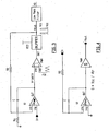
- Fig. 1 shows the typical scheme of a Class-D amplifier.
- This type of amplifier is a well-known PWM system (re: K. Nielsen, "Review and Comparison of PWM methods for analog and digital input switching power amplifiers” AES 22-25/3/97).
- the input signal ( Vin ) is compared with a waveform, most often triangular ( Vtr ) having a relatively high frequency fsw much higher than the frequency band limit of the amplifier.
- the output ( Vout ) is a PWM (Pulse Width Modulated) signal switching between a positive voltage ( Vcc ) and a negative voltage ( -Vcc ).
- Vo and Vin are thereby theoretically linear. In practice though this is not true because the non-idealities of the triangular wave and of the output buffer stage may produce an unacceptable amount of distortion on the output signal.
- a feedback loop capable of compensating the non-idealities of the system is a must.
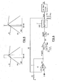
- FIG. 3 A typical feedback circuit is shown in Fig. 3
- The. open loop gain Gloop of the system may be easily calculated by analyzing the scheme of Fig. 4, wherein a linearized system is considered with the Vin node short-circuited to ground and the PWM stage substituted with a linear block with a gain Vcc/Vtr (re: equation 2).
- the input resistor R1 has been neglected because, at the frequencies of interest, the negative input of the integrator represents a virtual ground (because the integrating capacitor C represents an extremely low impedance) and therefore there is not any significative voltage drop on the input resistor R1 .
- This system has a stability limit that limits the system's bandwidth.
- This limit may be calculated (by referring to Fig. 3) by considering that for a correct functioning of the system, the slope of the ripple signal ( Vr ) must be lower than the slope of the triangular wave ( Vtr ).
- the system may produce repeated output switchings at intervals equal to the delay of the chain delay defined by the PWM stage and by the output buffer stage.
- the maximum slope of the ripple signal should be considered, in other words the maximum input signal Vin max .
- equation (12) may simplified into the following equation: f 0 ⁇ fsw ⁇
- the amplifier of the present invention functions even when the slope of the triangular wave is lower than the slope of the ripple of the input signal without causing spurious repetitive switchings of the output signal.
- the invention is defined in claim 1.
- Fig. 6 The functional diagram of a class-D amplifier according to the present invention is shown in Fig. 6.
- the only element that is introduced is the block DELAY Td, coupled in the direct signal path, in cascade to the output of the comparator PWM and, preferably, before the output power stage BUFFER.
- the introduction of the delay changes the PWM stage gain (the larger is the introduced delay the lower is the gain).
- the most critical condition for the stability of a system with a delay block coincides with that of an average duty-cycle and not with that of maximum or minimum duty-cycle as it was the case in a known system.
- the PWM modulator may be considered, for bandwidth calculation, as a linear block with a voltage gain given by the ratio between the average of the output signal and the average of the ripple signal.
- the calculation entails three steps:
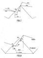
- Fig. 8 indicates the parameter notation adopted for the analysis and calculation.
- the problem is to establish the maximum admissible value of the parameter a without generating stability problems.
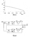
- the ratio ⁇ must be less than the limit value ⁇ max ., whose value is shown in the diagram of Fig. 8.
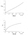
- a system with a ⁇ factor of about 1.6 may be implemented without any stability problems.
- the maximum value of the ⁇ factor for a certain delay Td (re: Fig. 9)
- the maximum bandwidth increment of the bandwidth ( ⁇ max. ) for the considered delay Td may be calculated.
- the improvement is of about 60%.
- the maximum usable delay is upper limited by the maximum duty-cycle at a certain switching frequency.
- the duty-cycle may range between 5% and 95% without skipping phenomena and with a bandwidth improvement factor of 1.5 referred to an amplifier made according to the prior art.
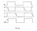
- the delay Td to be introduced may be larger than the minimum time Ton (or Toff ) of a phase of the PWM input signal, it is necessary to use two independent voltage ramps, respectively starting with the rising edge and with the falling edge of the digital input signal.
- Fig. 12 shows a possible circuit diagram of the delay block that is introduced in the direct signal path of the PWM signal in an amplifier realized according to the present invention.
- the slope of the voltage ramps is given by -I/C, where I is the discharge current of the capacitor C .
- the FF1 flip-flop When the input signal goes high, the FF1 flip-flop is set and the capacitor C is discharged at a constant current I .
- the voltage on the node A starts to decrease with a constant slope I/C.
- the reset of the flip-flop FF1 takes place when the input signal goes low.
- the reset of FF1 determines the reset of the voltage ramp (the node A switching to a high logic state).
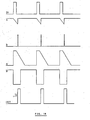
- Fig. 14 illustrates a condition when the duration of the high input phases Ton is shorter than the delay Td. It may be observed that in this case, the reset of the FF1 flip-flop follows directly the rising edge of the voltage on the node B. Therefore the duration of the set pulse of the output flip-flop FF 0 is determined solely by the delay of the flip-flop FF1 and of the pair of inverters.
Priority Applications (3)
| Application Number | Priority Date | Filing Date | Title |
|---|---|---|---|
| DE69926479T DE69926479D1 (de) | 1999-04-27 | 1999-04-27 | Klasse D Verstärker mit hoher Bandbreite |
| EP99830247A EP1049247B1 (fr) | 1999-04-27 | 1999-04-27 | Amplificateur classe D à grande largeur de bande |
| US09/557,364 US6346852B1 (en) | 1999-04-27 | 2000-04-25 | Class-D amplifier with enhanced bandwidth |
Applications Claiming Priority (1)
| Application Number | Priority Date | Filing Date | Title |
|---|---|---|---|
| EP99830247A EP1049247B1 (fr) | 1999-04-27 | 1999-04-27 | Amplificateur classe D à grande largeur de bande |
Publications (2)
| Publication Number | Publication Date |
|---|---|
| EP1049247A1 true EP1049247A1 (fr) | 2000-11-02 |
| EP1049247B1 EP1049247B1 (fr) | 2005-08-03 |
Family
ID=8243375
Family Applications (1)
| Application Number | Title | Priority Date | Filing Date |
|---|---|---|---|
| EP99830247A Expired - Lifetime EP1049247B1 (fr) | 1999-04-27 | 1999-04-27 | Amplificateur classe D à grande largeur de bande |
Country Status (3)
| Country | Link |
|---|---|
| US (1) | US6346852B1 (fr) |
| EP (1) | EP1049247B1 (fr) |
| DE (1) | DE69926479D1 (fr) |
Cited By (4)
| Publication number | Priority date | Publication date | Assignee | Title |
|---|---|---|---|---|
| EP1298794A2 (fr) * | 2001-09-26 | 2003-04-02 | Kabushiki Kaisha Toshiba | Circuit de réduction de bruit de commutation et amplificateur pour fréquences vocales |
| WO2003090343A2 (fr) | 2002-04-19 | 2003-10-30 | Koninklijke Philips Electronics N.V. | Amplificateur de puissance |
| EP1429455A1 (fr) * | 2002-12-11 | 2004-06-16 | Dialog Semiconductor GmbH | Linéarisation d'un amplificateur PDM de classe D |
| WO2010141193A3 (fr) * | 2009-05-16 | 2011-02-03 | Alcatel-Lucent Usa Inc. | Amplificateur de transimpédance doté d'une commande répartie de ligne de rétroaction |
Families Citing this family (15)
| Publication number | Priority date | Publication date | Assignee | Title |
|---|---|---|---|---|
| EP1178388B1 (fr) * | 2000-08-04 | 2006-06-28 | STMicroelectronics S.r.l. | Convertisseur MIC/MID avec amplificateur MID de puissance |
| EP1184973B1 (fr) * | 2000-08-29 | 2007-06-06 | STMicroelectronics S.r.l. | Equipement amplificateur de puissance |
| US6621335B2 (en) | 2001-04-18 | 2003-09-16 | Microsemi Corporation | Class D amplifier with passive RC network |
| GB0110340D0 (en) * | 2001-04-27 | 2001-06-20 | Watts Robert D | A signal processing circuit |
| US6404280B1 (en) * | 2001-06-01 | 2002-06-11 | Constel Signal Processing Co., Ltd. | Method and system for low-distortion power amplification |
| CN100547911C (zh) * | 2003-03-10 | 2009-10-07 | Nxp股份有限公司 | 三态d类放大器 |
| TWI220333B (en) * | 2003-06-12 | 2004-08-11 | Delta Electronics Inc | PWM buffer circuit for adjusting a frequency and a duty cycle of a PWM signal |
| US7772902B2 (en) | 2003-09-09 | 2010-08-10 | Delta Electronics, Inc. | PWM buffer circuit for adjusting a frequency and a duty cycle of a PWM signal |
| JP4710298B2 (ja) * | 2003-11-26 | 2011-06-29 | ヤマハ株式会社 | D級増幅器 |
| JP4452487B2 (ja) * | 2003-12-01 | 2010-04-21 | セイコーNpc株式会社 | D級増幅器 |
| US7683566B2 (en) * | 2007-01-30 | 2010-03-23 | Inventec Corporation | Fan rotation speed control circuit of power supply system |
| US7554391B1 (en) | 2008-01-11 | 2009-06-30 | Freescale Semiconductor, Inc. | Amplifier having a virtual ground and method thereof |
| US9595946B2 (en) | 2014-01-17 | 2017-03-14 | Stmicroelectronics S.R.L. | PWM modulator |
| CN103905006B (zh) * | 2014-03-28 | 2017-10-24 | 深圳创维-Rgb电子有限公司 | 一种具有占空比限制功能的d类功放芯片及其装置 |
| CN104104343B (zh) * | 2014-07-10 | 2017-09-29 | 矽力杰半导体技术(杭州)有限公司 | 应用于d类音频放大器的三角波产生方法及电路 |
Citations (2)
| Publication number | Priority date | Publication date | Assignee | Title |
|---|---|---|---|---|
| US4458208A (en) * | 1981-04-10 | 1984-07-03 | Sony Corporation | Pulse width modulated signal amplifier |
| US4649565A (en) * | 1982-09-02 | 1987-03-10 | U.S. Philips Corporation | Electro-acoustic converter with compensated frequency response characteristic |
Family Cites Families (3)
| Publication number | Priority date | Publication date | Assignee | Title |
|---|---|---|---|---|
| US5672998A (en) * | 1995-08-09 | 1997-09-30 | Harris Corporation | Class D amplifier and method |
| US5805020A (en) * | 1996-06-27 | 1998-09-08 | Harris Corporation | Silent start class D amplifier |
| US6016075A (en) * | 1997-06-04 | 2000-01-18 | Lord Corporation | Class-D amplifier input structure |
-
1999
- 1999-04-27 EP EP99830247A patent/EP1049247B1/fr not_active Expired - Lifetime
- 1999-04-27 DE DE69926479T patent/DE69926479D1/de not_active Expired - Lifetime
-
2000
- 2000-04-25 US US09/557,364 patent/US6346852B1/en not_active Expired - Lifetime
Patent Citations (2)
| Publication number | Priority date | Publication date | Assignee | Title |
|---|---|---|---|---|
| US4458208A (en) * | 1981-04-10 | 1984-07-03 | Sony Corporation | Pulse width modulated signal amplifier |
| US4649565A (en) * | 1982-09-02 | 1987-03-10 | U.S. Philips Corporation | Electro-acoustic converter with compensated frequency response characteristic |
Cited By (10)
| Publication number | Priority date | Publication date | Assignee | Title |
|---|---|---|---|---|
| EP1298794A2 (fr) * | 2001-09-26 | 2003-04-02 | Kabushiki Kaisha Toshiba | Circuit de réduction de bruit de commutation et amplificateur pour fréquences vocales |
| EP1298794A3 (fr) * | 2001-09-26 | 2003-10-22 | Kabushiki Kaisha Toshiba | Circuit de réduction de bruit de commutation et amplificateur pour fréquences vocales |
| US7142048B2 (en) | 2001-09-26 | 2006-11-28 | Kabushiki Kaisha Toshiba | Pop sound reduction circuit and voice output amplification device |
| WO2003090343A2 (fr) | 2002-04-19 | 2003-10-30 | Koninklijke Philips Electronics N.V. | Amplificateur de puissance |
| WO2003090343A3 (fr) * | 2002-04-19 | 2004-06-03 | Koninkl Philips Electronics Nv | Amplificateur de puissance |
| US7113038B2 (en) | 2002-04-19 | 2006-09-26 | Koninklijke Philips Electronics N.V. | Power amplifier |
| EP1429455A1 (fr) * | 2002-12-11 | 2004-06-16 | Dialog Semiconductor GmbH | Linéarisation d'un amplificateur PDM de classe D |
| US6771121B2 (en) | 2002-12-11 | 2004-08-03 | Dialog Semiconductor Gmbh | Linearization of a PDM Class-D amplifier |
| WO2010141193A3 (fr) * | 2009-05-16 | 2011-02-03 | Alcatel-Lucent Usa Inc. | Amplificateur de transimpédance doté d'une commande répartie de ligne de rétroaction |
| CN102428645A (zh) * | 2009-05-16 | 2012-04-25 | 阿尔卡特朗讯 | 具有分布式反馈线路控制的跨阻抗放大器 |
Also Published As
| Publication number | Publication date |
|---|---|
| US6346852B1 (en) | 2002-02-12 |
| DE69926479D1 (de) | 2005-09-08 |
| EP1049247B1 (fr) | 2005-08-03 |
Similar Documents
| Publication | Publication Date | Title |
|---|---|---|
| EP1049247B1 (fr) | Amplificateur classe D à grande largeur de bande | |
| EP0503571B1 (fr) | Amplificateur à modulation de largeur d'impulsion | |
| JP3982342B2 (ja) | D級増幅器における三角波生成回路および該三角波生成回路を用いたd級増幅器 | |
| US6362683B1 (en) | Break-before-make distortion compensation for a digital amplifier | |
| KR100617960B1 (ko) | 자가 발진형 펄스 폭 변조회로 및 펄스 폭 변조 방법 | |
| KR100775184B1 (ko) | D-급 증폭기 | |
| US7221216B2 (en) | Self-oscillating switching amplifier | |
| KR100435182B1 (ko) | Pwm 부궤환에 의한 디지털 pwm 입력 d급 음향 증폭기 | |
| KR100600507B1 (ko) | 펄스폭 변조 회로 | |
| US6489841B2 (en) | Class D audio amplifier | |
| KR20040015383A (ko) | 아날로그 fir 필터 | |
| US10560082B2 (en) | Pulse width modulation circuit, corresponding device and method | |
| WO2000022727A1 (fr) | Modulateur de classe d a frequence variable a ecretage a niveau variable et limitation de frequence integres | |
| JP4566566B2 (ja) | 電力増幅装置 | |
| US7545207B2 (en) | Control circuit and method for a switching amplifier | |
| US6956431B2 (en) | Pulse width modulation amplifier | |
| JPS628619A (ja) | デジタル−アナログ変換器 | |
| US7388426B2 (en) | Control circuit and method for a switching amplifier | |
| US6750705B2 (en) | Class D amplifier energy control | |
| JP4305275B2 (ja) | Pwm変調における過変調防止回路 | |
| US9991852B2 (en) | System and method for close-down pop reduction | |
| EP2750289B9 (fr) | Modulateur de largeur d'impulsion et amplificateur de commutation | |
| JP4947307B2 (ja) | スイッチングアンプ | |
| JPH0260089B2 (fr) | ||
| JPS59117667A (ja) | 時分割掛算回路 |
Legal Events
| Date | Code | Title | Description |
|---|---|---|---|
| PUAI | Public reference made under article 153(3) epc to a published international application that has entered the european phase |
Free format text: ORIGINAL CODE: 0009012 |
|
| AK | Designated contracting states |
Kind code of ref document: A1 Designated state(s): DE FR GB IT |
|
| AX | Request for extension of the european patent |
Free format text: AL;LT;LV;MK;RO;SI |
|
| 17P | Request for examination filed |
Effective date: 20001113 |
|
| AKX | Designation fees paid |
Free format text: DE FR GB IT |
|
| GRAP | Despatch of communication of intention to grant a patent |
Free format text: ORIGINAL CODE: EPIDOSNIGR1 |
|
| GRAS | Grant fee paid |
Free format text: ORIGINAL CODE: EPIDOSNIGR3 |
|
| GRAA | (expected) grant |
Free format text: ORIGINAL CODE: 0009210 |
|
| AK | Designated contracting states |
Kind code of ref document: B1 Designated state(s): DE FR GB IT |
|
| REG | Reference to a national code |
Ref country code: GB Ref legal event code: FG4D |
|
| REF | Corresponds to: |
Ref document number: 69926479 Country of ref document: DE Date of ref document: 20050908 Kind code of ref document: P |
|
| PG25 | Lapsed in a contracting state [announced via postgrant information from national office to epo] |
Ref country code: DE Free format text: LAPSE BECAUSE OF FAILURE TO SUBMIT A TRANSLATION OF THE DESCRIPTION OR TO PAY THE FEE WITHIN THE PRESCRIBED TIME-LIMIT Effective date: 20051104 |
|
| PLBE | No opposition filed within time limit |
Free format text: ORIGINAL CODE: 0009261 |
|
| STAA | Information on the status of an ep patent application or granted ep patent |
Free format text: STATUS: NO OPPOSITION FILED WITHIN TIME LIMIT |
|
| 26N | No opposition filed |
Effective date: 20060504 |
|
| EN | Fr: translation not filed | ||
| PG25 | Lapsed in a contracting state [announced via postgrant information from national office to epo] |
Ref country code: FR Free format text: LAPSE BECAUSE OF FAILURE TO SUBMIT A TRANSLATION OF THE DESCRIPTION OR TO PAY THE FEE WITHIN THE PRESCRIBED TIME-LIMIT Effective date: 20060929 |
|
| PGFP | Annual fee paid to national office [announced via postgrant information from national office to epo] |
Ref country code: IT Payment date: 20070608 Year of fee payment: 9 |
|
| PG25 | Lapsed in a contracting state [announced via postgrant information from national office to epo] |
Ref country code: FR Free format text: LAPSE BECAUSE OF FAILURE TO SUBMIT A TRANSLATION OF THE DESCRIPTION OR TO PAY THE FEE WITHIN THE PRESCRIBED TIME-LIMIT Effective date: 20050803 |
|
| PG25 | Lapsed in a contracting state [announced via postgrant information from national office to epo] |
Ref country code: IT Free format text: LAPSE BECAUSE OF NON-PAYMENT OF DUE FEES Effective date: 20080427 |
|
| PGFP | Annual fee paid to national office [announced via postgrant information from national office to epo] |
Ref country code: GB Payment date: 20100329 Year of fee payment: 12 |
|
| GBPC | Gb: european patent ceased through non-payment of renewal fee |
Effective date: 20110427 |
|
| PG25 | Lapsed in a contracting state [announced via postgrant information from national office to epo] |
Ref country code: GB Free format text: LAPSE BECAUSE OF NON-PAYMENT OF DUE FEES Effective date: 20110427 |