EP1297937B1 - Spachtel zur Herstellung von Rippen in Flachbildschirmen und sein Herstellungsverfahren - Google Patents
Spachtel zur Herstellung von Rippen in Flachbildschirmen und sein Herstellungsverfahren Download PDFInfo
- Publication number
- EP1297937B1 EP1297937B1 EP02021722A EP02021722A EP1297937B1 EP 1297937 B1 EP1297937 B1 EP 1297937B1 EP 02021722 A EP02021722 A EP 02021722A EP 02021722 A EP02021722 A EP 02021722A EP 1297937 B1 EP1297937 B1 EP 1297937B1
- Authority
- EP
- European Patent Office
- Prior art keywords
- blade
- compound layer
- hard particles
- comb teeth
- ribs
- Prior art date
- Legal status (The legal status is an assumption and is not a legal conclusion. Google has not performed a legal analysis and makes no representation as to the accuracy of the status listed.)
- Expired - Lifetime
Links
- 238000004519 manufacturing process Methods 0.000 title claims description 19
- 150000001875 compounds Chemical class 0.000 claims description 59
- 239000000758 substrate Substances 0.000 claims description 58
- 239000002245 particle Substances 0.000 claims description 42
- 239000000919 ceramic Substances 0.000 claims description 23
- 238000000034 method Methods 0.000 claims description 21
- 229910052751 metal Inorganic materials 0.000 claims description 15
- 239000002184 metal Substances 0.000 claims description 15
- MCMNRKCIXSYSNV-UHFFFAOYSA-N Zirconium dioxide Chemical compound O=[Zr]=O MCMNRKCIXSYSNV-UHFFFAOYSA-N 0.000 claims description 12
- 229910003460 diamond Inorganic materials 0.000 claims description 11
- 239000010432 diamond Substances 0.000 claims description 11
- 239000000463 material Substances 0.000 claims description 10
- 229910052759 nickel Inorganic materials 0.000 claims description 10
- HBMJWWWQQXIZIP-UHFFFAOYSA-N silicon carbide Chemical compound [Si+]#[C-] HBMJWWWQQXIZIP-UHFFFAOYSA-N 0.000 claims description 10
- 229910001220 stainless steel Inorganic materials 0.000 claims description 9
- 239000010935 stainless steel Substances 0.000 claims description 9
- 229910010271 silicon carbide Inorganic materials 0.000 claims description 7
- 229910018104 Ni-P Inorganic materials 0.000 claims description 6
- 229910018536 Ni—P Inorganic materials 0.000 claims description 6
- 229910052581 Si3N4 Inorganic materials 0.000 claims description 6
- 239000000654 additive Substances 0.000 claims description 6
- PNEYBMLMFCGWSK-UHFFFAOYSA-N aluminium oxide Inorganic materials [O-2].[O-2].[O-2].[Al+3].[Al+3] PNEYBMLMFCGWSK-UHFFFAOYSA-N 0.000 claims description 6
- HQVNEWCFYHHQES-UHFFFAOYSA-N silicon nitride Chemical compound N12[Si]34N5[Si]62N3[Si]51N64 HQVNEWCFYHHQES-UHFFFAOYSA-N 0.000 claims description 6
- MTPVUVINMAGMJL-UHFFFAOYSA-N trimethyl(1,1,2,2,2-pentafluoroethyl)silane Chemical compound C[Si](C)(C)C(F)(F)C(F)(F)F MTPVUVINMAGMJL-UHFFFAOYSA-N 0.000 claims description 6
- 229910052582 BN Inorganic materials 0.000 claims description 5
- 229910017709 Ni Co Inorganic materials 0.000 claims description 5
- 229910003267 Ni-Co Inorganic materials 0.000 claims description 5
- 229910003262 Ni‐Co Inorganic materials 0.000 claims description 5
- NRTOMJZYCJJWKI-UHFFFAOYSA-N Titanium nitride Chemical compound [Ti]#N NRTOMJZYCJJWKI-UHFFFAOYSA-N 0.000 claims description 5
- 230000000996 additive effect Effects 0.000 claims description 5
- 229910052796 boron Inorganic materials 0.000 claims description 5
- INAHAJYZKVIDIZ-UHFFFAOYSA-N boron carbide Chemical compound B12B3B4C32B41 INAHAJYZKVIDIZ-UHFFFAOYSA-N 0.000 claims description 5
- KZHJGOXRZJKJNY-UHFFFAOYSA-N dioxosilane;oxo(oxoalumanyloxy)alumane Chemical compound O=[Si]=O.O=[Si]=O.O=[Al]O[Al]=O.O=[Al]O[Al]=O.O=[Al]O[Al]=O KZHJGOXRZJKJNY-UHFFFAOYSA-N 0.000 claims description 5
- 239000010954 inorganic particle Substances 0.000 claims description 5
- 229910052863 mullite Inorganic materials 0.000 claims description 5
- 229910052721 tungsten Inorganic materials 0.000 claims description 5
- UONOETXJSWQNOL-UHFFFAOYSA-N tungsten carbide Chemical compound [W+]#[C-] UONOETXJSWQNOL-UHFFFAOYSA-N 0.000 claims description 5
- PMHQVHHXPFUNSP-UHFFFAOYSA-M copper(1+);methylsulfanylmethane;bromide Chemical compound Br[Cu].CSC PMHQVHHXPFUNSP-UHFFFAOYSA-M 0.000 claims description 4
- 239000003623 enhancer Substances 0.000 claims description 4
- 239000011521 glass Substances 0.000 description 15
- 239000003795 chemical substances by application Substances 0.000 description 12
- PXHVJJICTQNCMI-UHFFFAOYSA-N nickel Substances [Ni] PXHVJJICTQNCMI-UHFFFAOYSA-N 0.000 description 12
- 239000011248 coating agent Substances 0.000 description 11
- 238000000576 coating method Methods 0.000 description 11
- 230000000052 comparative effect Effects 0.000 description 6
- 238000001035 drying Methods 0.000 description 5
- 238000007747 plating Methods 0.000 description 5
- 238000007639 printing Methods 0.000 description 5
- 238000005282 brightening Methods 0.000 description 4
- 239000006185 dispersion Substances 0.000 description 4
- 238000009713 electroplating Methods 0.000 description 4
- 238000010438 heat treatment Methods 0.000 description 4
- 239000003381 stabilizer Substances 0.000 description 4
- 230000015572 biosynthetic process Effects 0.000 description 3
- 230000000694 effects Effects 0.000 description 3
- 238000007373 indentation Methods 0.000 description 3
- 238000002156 mixing Methods 0.000 description 3
- 239000000843 powder Substances 0.000 description 3
- 238000005488 sandblasting Methods 0.000 description 3
- VEXZGXHMUGYJMC-UHFFFAOYSA-N Hydrochloric acid Chemical compound Cl VEXZGXHMUGYJMC-UHFFFAOYSA-N 0.000 description 2
- 238000000137 annealing Methods 0.000 description 2
- 239000011230 binding agent Substances 0.000 description 2
- 230000007423 decrease Effects 0.000 description 2
- 238000011161 development Methods 0.000 description 2
- 238000007650 screen-printing Methods 0.000 description 2
- ORTVZLZNOYNASJ-UPHRSURJSA-N (z)-but-2-ene-1,4-diol Chemical compound OC\C=C/CO ORTVZLZNOYNASJ-UPHRSURJSA-N 0.000 description 1
- PIGFYZPCRLYGLF-UHFFFAOYSA-N Aluminum nitride Chemical compound [Al]#N PIGFYZPCRLYGLF-UHFFFAOYSA-N 0.000 description 1
- 229910021586 Nickel(II) chloride Inorganic materials 0.000 description 1
- KGBXLFKZBHKPEV-UHFFFAOYSA-N boric acid Chemical compound OB(O)O KGBXLFKZBHKPEV-UHFFFAOYSA-N 0.000 description 1
- 239000004327 boric acid Substances 0.000 description 1
- 239000000470 constituent Substances 0.000 description 1
- 238000005260 corrosion Methods 0.000 description 1
- 230000007797 corrosion Effects 0.000 description 1
- 229910052593 corundum Inorganic materials 0.000 description 1
- 239000007822 coupling agent Substances 0.000 description 1
- 230000003247 decreasing effect Effects 0.000 description 1
- 238000007598 dipping method Methods 0.000 description 1
- 238000007606 doctor blade method Methods 0.000 description 1
- 238000011156 evaluation Methods 0.000 description 1
- 238000010030 laminating Methods 0.000 description 1
- 239000004973 liquid crystal related substance Substances 0.000 description 1
- 238000000691 measurement method Methods 0.000 description 1
- 239000007769 metal material Substances 0.000 description 1
- 239000000203 mixture Substances 0.000 description 1
- QMMRZOWCJAIUJA-UHFFFAOYSA-L nickel dichloride Chemical compound Cl[Ni]Cl QMMRZOWCJAIUJA-UHFFFAOYSA-L 0.000 description 1
- 230000000149 penetrating effect Effects 0.000 description 1
- ACVYVLVWPXVTIT-UHFFFAOYSA-N phosphinic acid Chemical compound O[PH2]=O ACVYVLVWPXVTIT-UHFFFAOYSA-N 0.000 description 1
- 150000003016 phosphoric acids Chemical class 0.000 description 1
- 239000004033 plastic Substances 0.000 description 1
- 125000002924 primary amino group Chemical group [H]N([H])* 0.000 description 1
- -1 saccharin Chemical class 0.000 description 1
- CVHZOJJKTDOEJC-UHFFFAOYSA-N saccharin Chemical compound C1=CC=C2C(=O)NS(=O)(=O)C2=C1 CVHZOJJKTDOEJC-UHFFFAOYSA-N 0.000 description 1
- 229940081974 saccharin Drugs 0.000 description 1
- 235000019204 saccharin Nutrition 0.000 description 1
- 239000000901 saccharin and its Na,K and Ca salt Substances 0.000 description 1
- FZHAPNGMFPVSLP-UHFFFAOYSA-N silanamine Chemical compound [SiH3]N FZHAPNGMFPVSLP-UHFFFAOYSA-N 0.000 description 1
- HUAUNKAZQWMVFY-UHFFFAOYSA-M sodium;oxocalcium;hydroxide Chemical compound [OH-].[Na+].[Ca]=O HUAUNKAZQWMVFY-UHFFFAOYSA-M 0.000 description 1
- 150000003464 sulfur compounds Chemical class 0.000 description 1
- 238000012360 testing method Methods 0.000 description 1
- 239000002699 waste material Substances 0.000 description 1
- 229910001845 yogo sapphire Inorganic materials 0.000 description 1
Images


Classifications
-
- H—ELECTRICITY
- H01—ELECTRIC ELEMENTS
- H01J—ELECTRIC DISCHARGE TUBES OR DISCHARGE LAMPS
- H01J9/00—Apparatus or processes specially adapted for the manufacture, installation, removal, maintenance of electric discharge tubes, discharge lamps, or parts thereof; Recovery of material from discharge tubes or lamps
- H01J9/24—Manufacture or joining of vessels, leading-in conductors or bases
-
- H—ELECTRICITY
- H01—ELECTRIC ELEMENTS
- H01J—ELECTRIC DISCHARGE TUBES OR DISCHARGE LAMPS
- H01J9/00—Apparatus or processes specially adapted for the manufacture, installation, removal, maintenance of electric discharge tubes, discharge lamps, or parts thereof; Recovery of material from discharge tubes or lamps
- H01J9/24—Manufacture or joining of vessels, leading-in conductors or bases
- H01J9/241—Manufacture or joining of vessels, leading-in conductors or bases the vessel being for a flat panel display
- H01J9/242—Spacers between faceplate and backplate
-
- B—PERFORMING OPERATIONS; TRANSPORTING
- B29—WORKING OF PLASTICS; WORKING OF SUBSTANCES IN A PLASTIC STATE IN GENERAL
- B29C—SHAPING OR JOINING OF PLASTICS; SHAPING OF MATERIAL IN A PLASTIC STATE, NOT OTHERWISE PROVIDED FOR; AFTER-TREATMENT OF THE SHAPED PRODUCTS, e.g. REPAIRING
- B29C59/00—Surface shaping of articles, e.g. embossing; Apparatus therefor
- B29C59/02—Surface shaping of articles, e.g. embossing; Apparatus therefor by mechanical means, e.g. pressing
- B29C59/026—Surface shaping of articles, e.g. embossing; Apparatus therefor by mechanical means, e.g. pressing of layered or coated substantially flat surfaces
-
- H—ELECTRICITY
- H01—ELECTRIC ELEMENTS
- H01J—ELECTRIC DISCHARGE TUBES OR DISCHARGE LAMPS
- H01J11/00—Gas-filled discharge tubes with alternating current induction of the discharge, e.g. alternating current plasma display panels [AC-PDP]; Gas-filled discharge tubes without any main electrode inside the vessel; Gas-filled discharge tubes with at least one main electrode outside the vessel
- H01J11/20—Constructional details
- H01J11/34—Vessels, containers or parts thereof, e.g. substrates
- H01J11/36—Spacers, barriers, ribs, partitions or the like
-
- B—PERFORMING OPERATIONS; TRANSPORTING
- B29—WORKING OF PLASTICS; WORKING OF SUBSTANCES IN A PLASTIC STATE IN GENERAL
- B29C—SHAPING OR JOINING OF PLASTICS; SHAPING OF MATERIAL IN A PLASTIC STATE, NOT OTHERWISE PROVIDED FOR; AFTER-TREATMENT OF THE SHAPED PRODUCTS, e.g. REPAIRING
- B29C59/00—Surface shaping of articles, e.g. embossing; Apparatus therefor
- B29C59/02—Surface shaping of articles, e.g. embossing; Apparatus therefor by mechanical means, e.g. pressing
- B29C2059/027—Grinding; Polishing
-
- B—PERFORMING OPERATIONS; TRANSPORTING
- B29—WORKING OF PLASTICS; WORKING OF SUBSTANCES IN A PLASTIC STATE IN GENERAL
- B29K—INDEXING SCHEME ASSOCIATED WITH SUBCLASSES B29B, B29C OR B29D, RELATING TO MOULDING MATERIALS OR TO MATERIALS FOR MOULDS, REINFORCEMENTS, FILLERS OR PREFORMED PARTS, e.g. INSERTS
- B29K2995/00—Properties of moulding materials, reinforcements, fillers, preformed parts or moulds
- B29K2995/0037—Other properties
- B29K2995/0087—Wear resistance
-
- H—ELECTRICITY
- H01—ELECTRIC ELEMENTS
- H01J—ELECTRIC DISCHARGE TUBES OR DISCHARGE LAMPS
- H01J2211/00—Plasma display panels with alternate current induction of the discharge, e.g. AC-PDPs
- H01J2211/20—Constructional details
- H01J2211/34—Vessels, containers or parts thereof, e.g. substrates
- H01J2211/36—Spacers, barriers, ribs, partitions or the like
Definitions
- the present invention relates to a blade for forming ribs and its production method for easily and accurately forming ribs (ceramic capillary ribs) in the production process of FPD (flat panel displays) such as PDP (plasma display panels) and PALC (plastic addressed liquid crystal displays).
- FPD flat panel displays
- PDP plasma display panels
- PALC plastic addressed liquid crystal displays
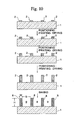
- ribs 8 are made by positioning a rib-forming paste 2 containing glass powder on a glass substrate 1 in a prescribed pattern by a thick film printing method, coating several layers of the paste, and baking the paste after drying to form ribs 8 at prescribed intervals on substrate 1 as shown in FIG. 10 .
- the height H of rib 8 is normally 100-300 ⁇ m
- rib width W is normally about 50-100 ⁇ m
- the spread S of cell 9 between the ribs is normally about 100-300 ⁇ m.
- the sandblasting method is known as a second method of forming ribs.
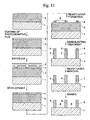
- a ceramic paste containing glass powder is coated onto the entire surface of a glass substrate 1 using a thick film method, and after forming pattern forming layer 3 having a height of 150-200 ⁇ m by drying or laminating ceramic green tape containing glass powder, this pattern forming layer 3 is coated with a photosensitive film 4, and this film 4 is further covered with a mask 5 followed by exposure and development to form resist layer 6 of a prescribed pattern as shown in FIG. 11 .
- the above resist layer 6 is removed using a remover and so forth to obtain the desired ribs 8.
- the above second forming method of the prior art requires the coating of a photosensitive film to form the resist layer as well as complicated steps such as exposure and development.
- the object of the present invention is to provide a blade for forming ribs that is able to improve wear resistance.
- Another object of the present invention is to provide a production method of a blade that lowers the frequency of blade replacement and improves the accuracy of the ribs that are formed.
- One aspect of the invention is according to claim 1, another aspect is according to claim 9.
- the present invention provide, as shown in FIG. 2 , a blade for forming ribs 13, either on the surface of a substrate 10 or via an undercoating layer on the surface of a substrate, by moving a blade body 12 in a fixed direction relative to a paste film 11 in the state in which comb teeth 12b formed on at least a portion of the periphery of blade body 12 are penetrated into a ceramic paste film 11 formed on the surface of substrate 10 to plasticly deform paste film 11, the surface of comb teeth 12b formed on blade body 12 that makes contact with paste film 11 is coated with a compound layer 12c in which hard particles are dispersed in a metal.
- the material of the comb teeth prefferably be stainless steel.
- the compound layer it is also preferable for the compound layer to contain 1-50% by volume of hard particles with respect to 100% by volume of the compound layer.
- the thickness of the compound layer it is also preferable for the thickness of the compound layer to be 0.1-20 ⁇ m.
- the metal of the compound layer prefferably be selected from the group consisting of Ni, Ni-P, Ni-B, Ni-W, Ni-Co and Co.
- the Vickers hardness H of the hard particles of compound layer it is also preferable for the Vickers hardness H of the hard particles of compound layer to be 1,000 or more.
- the hard particles of the compound layer are one type or two or more types of inorganic particles selected from diamond, amorphous diamond, silicon carbide, c-boron nitride, silicon nitride, alumina, tungsten carbide, titanium carbide, titanium nitride, tetraboron carbide, mullite, aluminum nitride and zirconia.
- the average particle diameter of the hard particles it is also preferable for the average particle diameter of the hard particles to be 0.1-10 ⁇ m.
- the additive in the blade, it is also preferable for the additive to be a microcrystallizing agent, stress relief agent, brightening agent, dispersion stabilizer or surface potential controller.
- the present invention provides a method of producing a blade for forming ribs 13 and 23 either on the surface of a substrate 10 or via an undercoating layer 22 on the surface of substrate 10 by moving a blade body 12 in a fixed direction relative to a paste film 11 in the state in which comb teeth 12b formed on at least a portion of the periphery of blade body 12 are penetrated into ceramic paste film 11 formed on the surface of substrate 10 to plasticly deform paste film 11; comprising the step of: a step in which in which comb teeth 12b are formed on one edge of a plate-shaped blade body 12 made of ceramic or metal; and a step in which the surface of comb teeth 12b is coated with a compound layer 12c in which hard particles are dispersed in a metal.
- the replacement frequency of the blade can be lowered and the accuracy of the ribs that are formed can be improved.
- the material of the comb teeth prefferably be stainless steel.
- the compound layer in the blade production method, it is also preferable for the compound layer to contain 1-50% by volume of hard particles with respect to 100% by volume of the compound layer.
- the thickness of the compound layer it is also preferable for the thickness of the compound layer to be 0.1-20 ⁇ m.
- the metal of compound layer prefferably be selected from the group consisting of Ni, Ni-P, Ni-B, Ni-W, Ni-Co and Co.
- the Vickers hardness H of the hard particles of compound layer is 1,000 or more.
- the hard particles of compound layer prefferably be one type or two or more types of inorganic particles selected from diamond, amorphous diamond, silicon carbide, c-boron nitride, silicon nitride, alumina, tungsten carbide, titanium carbide, titanium nitride, tetraboron carbide, mullite, aluminum nitride and zirconia.
- the average particle diameter of the hard particles it is also preferable for the average particle diameter of the hard particles to be 0.1-10 ⁇ m.
- the additive in the blade production method, it is also preferable for the additive to be a microcrystallizing agent, stress relief agent, brightening agent, dispersion stabilizer, or a surface potential controller.
- a plurality of comb teeth 12b are formed at equal intervals and in the same direction on one edge of plate-shaped blade body 12 made of ceramic or metal as shown in FIGS. 4 and 5 .
- the characteristic constitution of the blade for forming ribs of the present invention lies in the coating of the surface of comb teeth 12b formed on blade body 12 that make contact with paste film 11 with a compound layer 12c in which hard particles are dispersed in a metal.
- Stainless steel having superior corrosion resistance that is not react with the paste and is not dissolved in the paste is used for the material of comb teeth 12b.
- the compound layer 12c that coats the surface of comb teeth 12b contains hard particles at a ratio of 1-50 % by volume to 100 % by volume of the compound layer. If the blending ratio of hard particles is less than the 1% by volume, the effect of improving wear resistance is small, and if the blending ratio exceeds 50% by volume, the fixing of hard particles to the film is inadequate, causing them to fall off during the course of wear.
- the blending ratio of hard particles is preferably 3-20 % by volume.
- the thickness of the coated compound layer is 0.1-20 ⁇ m. If the thickness is less than 0.1 ⁇ m, the effect of improving wear resistance is small, and if the thickness exceeds 20 ⁇ m, cracks form in the compound layer or the compound layer comes off of the blade base material during rib formation.
- the thickness of the coated compound layer is preferably 1-10 ⁇ m.
- the metal material of compound layer 12c is selected from the group consisting of Ni, Ni-P, Ni-B, Ni-W, Ni-Co and Co. Among these, Ni, Ni-P and Ni-B are preferable from the viewpoint of material cost and characteristics.
- the hard particles of compound layer 12c have a Vickers hardness of 1,000 or more.
- Vickers hardness HV is one kind of indentation hardness, and is typically used as one of the values for expressing the hardness of an object.
- the measurement method consists of using a diamond quadrangular pyramid having an angle between opposing sides of 136° as an indenter, and determining the length of the diagonal line of the square indentation that results when that indenter is pressed into the sample at a fixed load. The surface area of the indentation is then determined from the length of this diagonal line, and value obtained by dividing the load by the surface area is obtained as the Vickers hardness. This Vickers hardness is expressed as a value only without units.
- the material of the hard particles is one type or two or more types of inorganic particles selected from diamond, amorphous diamond (DLC), silicon carbide (SiC), c-boron nitride (c-BN), silicon nitride (Si 3 N 4 ), alumina (Al 2 O 3 ), tungsten carbide (WC), titanium carbide (TiC), titanium nitride (TiN), tetraboron carbide (B 4 C), mullite, aluminum nitride (AlN) and zirconia (ZrO 2 ).
- silicon carbide is preferable from the viewpoint of material cost and characteristics.
- the average particle diameter of the hard particles is 0.1-10 ⁇ m. If the average particle diameter is less than 0.1 ⁇ m, the effect of improving wear resistance is small, and if the average particle diameter exceeds 10 ⁇ m, variations in the shape of the blade openings become large.
- the average particle diameter of the hard particles is preferably 1-5 ⁇ m.
- Blade durability and accuracy of the intervals between the ribs formed using this blade are improved by additionally containing an additive in the compound layer.
- additives include a microcrystallizing agent, stress relief agent, brightening agent, dispersion stabilizer, surface potential controller and hardness enhancer. More specifically, examples of microcrystallizing agents and stress relief agents include sulfur compounds such as saccharin, examples of brightening agents include butenediol, examples of hard particle dispersion stabilizers and surface potential controllers include amino compounds such as aminosilane coupling agents, and examples of hardness enhancers include phosphoric acid compounds such as hypophosphorous acid.
- Examples of methods for coating the surface of comb teeth 12b with the compound layer include electrolytic plating and non-electrolytic plating. Annealing treatment may also be performed after the compound layer is formed on the blade. The hardness of the compound layer can be increased by this annealing treatment.
- the following provides an explanation of an example of a method for coating the surface of the comb teeth of the blade with the compound layer using electrolytic plating.
- a stainless steel blade is degreased with base, and then cleaned with hydrochloric acid.
- nickel strike plating is performed on the surface of the blade.
- a compound plating bath is prepared in the ratio of 450 g/l of nickel sulfaminate, 5 g/l of nickel chloride, 30 g/l of boric acid and 50 g/l of silicon carbide powder having an average particle diameter of 3.0 ⁇ m.
- the blade is immersed in the prepared compound plating bath as the cathode, while a plate made of nickel metal is immersed in the compound plating bath as the anode.
- a compound plated film is formed on the stainless steel blade serving as the cathode under conditions of a cathode current density of 5 A/dm 2 , plating time of 10 min., pH of 4.0 and bath temperature of 45°C.
- a compound plated film having a film thickness of 5 ⁇ m can be formed on the stainless steel blade.
- the amount of silicon carbide powder contained in this compound plated film is 10 % by volume.
- the respective gaps between comb teeth 12b are formed corresponding to the cross-sectional shape of the ribs formed by this blade 12.
- the shape of the gaps of comb teeth 12b is not only the case of forming a rectangular shape as shown in FIG. 4 , but rather the shape of the gaps of comb teeth 12b may form a trapezoidal shape or inverted trapezoidal shape according to the application of the FPD ultimately produced. If the shape of the gaps of comb teeth 12b is made to be trapezoidal, ribs 13 can be formed that are suited for applications having wide openings, while if the shape of the gaps of comb teeth 12b is made to be inverted trapezoidal, ribs 13 can be formed in which the apices of the ribs have a wide area and are flat.
- a paste is first coated onto substrate 10 to form ceramic paste 11 on its surface.
- suitable substrates in the present invention include glass substrate 10 only shown in FIG. 8A , glass substrate 10 on which electrodes 16 are formed on its surface shown in FIG. 8B , and glass substrate 10 on which an undercoating layer 17 made of ceramic and so forth is formed on the surface shown in FIG. 8C .
- glass substrate 10 on which undercoating layer 17 is formed on its surface is suitable for using the blade of the present invention. Coating of paste onto the surface of substrate 10 is carried out by a known means such as screen printing, dipping or doctor blade coating.
- comb teeth 12b formed on at least a portion of the periphery of blade body 12 are penetrated into paste film 11 formed by coating a paste onto the surface of substrate 10, and edge 12a of blade 12 is brought into contact with the surface of substrate 10 on which paste film 11 has been formed.
- edge 12a is in contact with the surface of substrate 10
- either blade 12 is moved in a fixed direction as indicated with the solid line arrow of FIG. 2 while fixing substrate 10, or substrate 10 is moved in a fixed direction as shown with the broken line arrow of FIG. 2 while fixing blade 12, to plasticly deform paste film 11.
- the locations corresponding to comb teeth 12b of blade 12 in the paste coated onto the surface of substrate 10 are those locations that move to the gaps between comb teeth 12b or are scratched off, and only the paste located in the gaps between comb teeth 12b remains on substrate 10 to form ribs 13 on the surface of substrate 10.
- the depth of the grooves of the comb teeth is greater than the thickness of paste film 11
- paste that is scratched off when blade 12 or glass substrate 10 is moved enters the grooves, allowing the formation of ribs 13 having a height equal to or greater than the thickness of paste film 11.
- Ribs 13 formed in this manner become ceramic ribs (not shown) by being subsequently dried, and by additionally heating to remove binder followed by baking, the ceramic ribs 14 shown in FIG. 3 are formed.
- FIGS. 6 and 7 The same reference symbols used in FIGS. 2 and 3 indicate the same constituent members in FIGS. 6 and 7 .
- the following points are different from the previously described method. Namely, by penetrating comb teeth 12b formed on blade 12 into paste film 11 formed by coating a paste onto the surface of substrate 10, and moving blade 12 or substrate 10 in a fixed direction in the state in which edge 12a of blade 12 is lifted from the surface of substrate 10 at a prescribed height, undercoating layer 22 and ribs 23 on this undercoating layer 22 can be formed on the surface of substrate 10.
- the constitution other than that described above is similar to the first embodiment for carrying out the invention.
- formation of ribs 23 by blade 12 is carried out by either moving blade 12 in a fixed direction as shown with the solid line arrow while fixing substrate 10, or moving substrate 10 in a fixed direction, in the state in which edge 12a of blade 12 is lifted from the surface of substrate 10 at a prescribed height.
- undercoating layer 22 is formed while leaving paste on the surface of the substrate to a prescribed height from the surface of substrate 10, and the locations corresponding to comb teeth 12b of blade 12 in the paste above this undercoating layer 22 either move to the gaps of comb teeth 12b or are scratched off, and only the paste located in the gaps of comb teeth 12b remains on undercoating layer 22, while ribs 23 are formed on undercoating layer 22.
- the undercoating layer 22 and ribs 23 formed in this manner are subsequently dried to form a ceramic green layer and ceramic green ribs (not shown), and as a result of heating to remove binder followed by baking, dielectric layer 24 is formed on the substrate as shown in FIG. 7 , and ceramic ribs 25 are formed on this dielectric layer 24.
- a soda lime-based glass substrate 10 was prepared having a diagonal dimension of (106.68cm) 42 inches and thickness of 3 mm.
- a ceramic paste was coated onto this glass substrate 10 followed by baking to form a ceramic undercoating layer having a thickness of 10 ⁇ m on the glass substrate.
- a paste was coated onto glass substrate 10 having an undercoating layer on its surface at a thickness of 350 ⁇ m by screen printing to form paste film 11.
- a blade 12 formed from stainless steel was prepared in which the pitch of comb teeth 12b was 360 ⁇ m, the gap w between comb teeth 12b was 180 ⁇ m, the depth was 350 ⁇ m, the thickness was 0.1 mm and the edge angle was 75 degrees ( FIGS. 4 and 5 ).
- the surface of comb teeth 12b of this blade 12 was coated with a compound layer in which hard particles in the form of silicon carbide particles were dispersed in nickel metal ( FIG. 1 ).
- the composition of this compound layer consisted of 10 % by volume of silicon carbide to 100 % by volume of the compound layer.
- Blade 12 Comb teeth 12b of this blade 12 were then penetrated into paste film 11 at a printing pressure of 18 MPa, and blade 12 was moved at the rate of 10 mm/sec in the direction indicated with the solid line arrow of FIG. 2 in the state in which its edge 12a was in contact with glass substrate 10 to plasticly deform paste film 11 and form ribs 13 on substrate 10.
- ribs 13 were formed on substrate 10 in the same manner as Example 1.
Landscapes
- Engineering & Computer Science (AREA)
- Manufacturing & Machinery (AREA)
- Mechanical Engineering (AREA)
- Physics & Mathematics (AREA)
- Plasma & Fusion (AREA)
- Gas-Filled Discharge Tubes (AREA)
- Other Surface Treatments For Metallic Materials (AREA)
- Coating Apparatus (AREA)
- Structures Of Non-Positive Displacement Pumps (AREA)
- Printing Plates And Materials Therefor (AREA)
Claims (16)
- Klinge (12) zur Ausbildung der Rippen eines flachen Anzeige-Paneels (13, 23) entweder auf der Oberfläche eines Substrats (10) oder eine Grundschicht (22) auf der Oberfläche eines Substrats (10) durch Bewegung des Klingenkörpers (12) in einer feststehenden Richtung in Bezug auf einen pastösen Film (11), der auf der Oberfläche des Substrats (10) ausgebildet ist, um den pastösen Film (11) plastisch zu deformieren, wobei die Klinge kammartige Zähne (12b) mit dazwischen liegenden Spalten aufweist, die mit der Querschnittsform der von der Klinge auszubildenden Rippen korrespondieren, wobei
die Oberfläche der kammartigen Zähne (12b), die in Kontakt mit dem pastösen Film zu bringen ist, mit einer Verbundschicht (12c) beschichtet ist, in der harte Partikel in einem Metall dispergiert sind, und
die Verbundschicht (12c) des Weiteren ein Additiv in der Form eines Härte-Verstärkers enthält. - Klinge (12) gemäß Anspruch 1, wobei das Material der kammartigen Zähne (12b) Edelstahl ist.
- Klinge (12) gemäß Anspruch 1 oder 2, wobei die Verbundschicht (12c) 1 bis 50 Vol-% der harten Partikel in Bezug auf 100 Vol-% der Verbundschicht enthält.
- Klinge (12) gemäß Anspruch 1, 2 oder 3, wobei die Dicke der Verbundschicht (12c) 0,1 bis 20 µm beträgt.
- Klinge (12) gemäß einem der voranstehenden Ansprüche, wobei das Metall der Verbundschicht (12b) aus Nickel, Ni-P, Ni-B, Ni-W, Ni-Co und Co ausgewählt ist.
- Klinge (12) gemäß einem der voranstehenden Ansprüche, wobei die Vickers-Härte H der harten Partikel der Verbundschicht (12c) 1000 oder höher ist.
- Klinge (12) gemäß einem der voranstehenden Ansprüche, wobei die harten Partikel der Verbundschicht (12c) anorganische Partikel eines oder mehrerer Arten sind, und aus Diamant, amorphem Diamant, Silizium-Karbid, C-Bornitrid, Silizium-Nitrid, Aluminiumoxid, Wolfram-Karbid, Titan-Karbid, Titan-Nitrid, Tetra-Borkarbid, Mullit, Aluminium-Nitrid und Zirkonoxid ausgewählt sind.
- Klinge (12) gemäß einem der voranstehenden Ansprüche, wobei der durchschnittliche Partikeldurchmesser der Härtepartikel 0,1 bis 10 µm beträgt.
- Verfahren zur Herstellung einer Klinge (12) gemäß Anspruch 1, wobei das Verfahren umfasst:einen Schritt, in dem die kammartigen Zähne (12c) an einer Kante eines plattenförmigen Klingenkörpers (12), der aus einer Keramik oder Metall gefertigt ist, ausgebildet werden, und gekennzeichnet durch:einen Schritt, bei dem die Oberfläche der kammartigen Zähne (12b) mit einer Verbundschicht (12c) beschichtet wird, in der harte Partikel in einem Metall dispergiert sind, wobei die Verbundschicht (12b) des Weiteren ein Additiv in der Form eines Härte-Verstärkers enthält.
- Klingen(12)-Herstellungsverfahren gemäß Anspruch 9, wobei das Material der kammartigen Zähne (12b) Edelstahl ist.
- Klingen(12)-Herstellungsverfahren gemäß Anspruch 9 oder 10, wobei die Verbundschicht (12c) 1 bis 50 Vol-% der harten Partikel in Bezug auf 100 Vol-% der Verbundschicht (12c) enthält.
- Klingen(12)-Herstellungsverfahren gemäß Anspruch 9, 10 oder 11, wobei die Dicke der Verbundschicht (12c) 0,1 bis 20 µm beträgt.
- Klingen(12)-Herstellungsverfahren gemäß einem der Ansprüche 9 bis 12, wobei das Metall der Verbundschicht (12c) aus Nickel, Nickel-Phosphor, Nickel-Bor, Nickel-Wolfram, Nickel-Kobalt und Kobalt ausgewählt ist.
- Klingen(12)-Herstellungsverfahren gemäß einem der Ansprüche 9 bis 13, wobei die Vickers-Härte H der Härtepartikel der Verbundschicht (12c) 1000 oder mehr beträgt.
- Klingen(12)-Herstellungsverfahren gemäß einem der Ansprüche 9 bis 14, wobei die harten Partikel der Verbundschicht (12c) ein oder zwei oder mehr harte anorganischer Partikel sind, die aus Diamant, amorphem Diamant, Silizium-Karbid, C-Bornitrid, Silizium-Nitrid, Aluminium-Oxid, Wolfram-Karbid, Titan-Karbid, Titan-Nitrid, Tetra-Borkarbid, Mullit, Aluminium-Nitrid oder Zirkonoxid ausgewählt sind.
- Klingen(12)-Herstellungsverfahren gemäß Anspruch 15, wobei der durchschnittliche Partikeldurchmesser der harten Partikel 0,1 bis 10 µm beträgt.
Applications Claiming Priority (2)
| Application Number | Priority Date | Filing Date | Title |
|---|---|---|---|
| JP2001296896 | 2001-09-27 | ||
| JP2001296896A JP3987701B2 (ja) | 2001-09-27 | 2001-09-27 | リブ状物の形成用ブレード及びこのブレードの製造方法 |
Publications (3)
| Publication Number | Publication Date |
|---|---|
| EP1297937A2 EP1297937A2 (de) | 2003-04-02 |
| EP1297937A3 EP1297937A3 (de) | 2005-08-10 |
| EP1297937B1 true EP1297937B1 (de) | 2009-07-29 |
Family
ID=19118059
Family Applications (1)
| Application Number | Title | Priority Date | Filing Date |
|---|---|---|---|
| EP02021722A Expired - Lifetime EP1297937B1 (de) | 2001-09-27 | 2002-09-25 | Spachtel zur Herstellung von Rippen in Flachbildschirmen und sein Herstellungsverfahren |
Country Status (7)
| Country | Link |
|---|---|
| US (1) | US6872115B2 (de) |
| EP (1) | EP1297937B1 (de) |
| JP (1) | JP3987701B2 (de) |
| KR (1) | KR100624829B1 (de) |
| CN (1) | CN100466144C (de) |
| DE (1) | DE60233100D1 (de) |
| TW (1) | TWI221308B (de) |
Families Citing this family (5)
| Publication number | Priority date | Publication date | Assignee | Title |
|---|---|---|---|---|
| SE519466C2 (sv) * | 2000-12-07 | 2003-03-04 | Swedev Ab | Schaber - eller rakelblad med beläggning av nickel innefattandes nötningsbeständiga partiklar och metod vid dess framställning |
| FR2818798B1 (fr) * | 2000-12-22 | 2003-02-21 | Thomson Multimedia Sa | Procede de fabrication d'un reseau de barrieres en materiau mineral sur une dalle pour panneau de visualisation a plasma |
| KR100450832B1 (ko) * | 2002-07-15 | 2004-10-12 | 엘지전자 주식회사 | 모세관 몰딩법에 의한 플라즈마 디스플레이 소자의 격벽제조방법 및 그것의 페이스트 조성물 |
| CN100538968C (zh) * | 2006-07-06 | 2009-09-09 | 东元电机股份有限公司 | 使阻隔壁厚度均匀化的方法 |
| US8725688B2 (en) * | 2008-09-05 | 2014-05-13 | Commvault Systems, Inc. | Image level copy or restore, such as image level restore without knowledge of data object metadata |
Family Cites Families (9)
| Publication number | Priority date | Publication date | Assignee | Title |
|---|---|---|---|---|
| JP3591910B2 (ja) * | 1995-03-30 | 2004-11-24 | 大日本印刷株式会社 | プラズマディスプレイパネルのセル障壁製造方法 |
| JPH10188793A (ja) * | 1996-10-21 | 1998-07-21 | Hitachi Ltd | ガス放電型表示パネル、ガス放電型表示パネルの製造方法およびガス放電型表示パネルを用いた表示装置 |
| DE69826359T2 (de) * | 1997-04-30 | 2005-09-29 | Kyocera Corp. | Hertellungsverfahren eines Substrats für eine Plasma-Anzeigeeinheit |
| JP2958298B2 (ja) * | 1997-05-22 | 1999-10-06 | 三星電管株式會社 | プラズマ表示素子の隔壁製造方法及びその製造装置 |
| KR100277633B1 (ko) * | 1997-12-23 | 2001-02-01 | 김순택 | 플라즈마디스플레이장치의격벽제조방법및그에의한플라즈마디스플레이장치 |
| JP3387833B2 (ja) | 1998-01-30 | 2003-03-17 | 三菱マテリアル株式会社 | セラミックキャピラリリブの形成方法及びこれを用いたセラミックリブの形成方法 |
| JP3346356B2 (ja) * | 1998-12-21 | 2002-11-18 | 三菱マテリアル株式会社 | リブ状物の形成装置 |
| JP3991500B2 (ja) * | 1999-04-16 | 2007-10-17 | 三菱マテリアル株式会社 | 基板表面にリブ状物を形成する方法及びその成形装置 |
| JP3565211B2 (ja) * | 2002-03-29 | 2004-09-15 | 三菱マテリアル株式会社 | リブ状物の形成装置 |
-
2001
- 2001-09-27 JP JP2001296896A patent/JP3987701B2/ja not_active Expired - Fee Related
-
2002
- 2002-09-23 TW TW091121766A patent/TWI221308B/zh not_active IP Right Cessation
- 2002-09-24 US US10/252,361 patent/US6872115B2/en not_active Expired - Fee Related
- 2002-09-24 KR KR1020020057876A patent/KR100624829B1/ko not_active Expired - Fee Related
- 2002-09-25 DE DE60233100T patent/DE60233100D1/de not_active Expired - Lifetime
- 2002-09-25 EP EP02021722A patent/EP1297937B1/de not_active Expired - Lifetime
- 2002-09-25 CN CNB021439516A patent/CN100466144C/zh not_active Expired - Fee Related
Also Published As
| Publication number | Publication date |
|---|---|
| CN1414592A (zh) | 2003-04-30 |
| KR20030026881A (ko) | 2003-04-03 |
| TWI221308B (en) | 2004-09-21 |
| US6872115B2 (en) | 2005-03-29 |
| JP3987701B2 (ja) | 2007-10-10 |
| EP1297937A2 (de) | 2003-04-02 |
| EP1297937A3 (de) | 2005-08-10 |
| JP2003109495A (ja) | 2003-04-11 |
| US20030056313A1 (en) | 2003-03-27 |
| CN100466144C (zh) | 2009-03-04 |
| DE60233100D1 (de) | 2009-09-10 |
| KR100624829B1 (ko) | 2006-09-18 |
Similar Documents
| Publication | Publication Date | Title |
|---|---|---|
| EP2103712B1 (de) | Ni-P-Schichtsystem und Zubereitungsverfahren | |
| KR102078293B1 (ko) | 유리 에칭 매질 및 방법 | |
| EP1297937B1 (de) | Spachtel zur Herstellung von Rippen in Flachbildschirmen und sein Herstellungsverfahren | |
| EP3293001A1 (de) | Laminierter körper mit korrosionsbeständiger beschichtung und verfahren zur herstellung davon | |
| ITMI20001287A1 (it) | Elettrodo caratterizzato da elevata adesione di uno strato cataliticosuperficiale. | |
| KR102549660B1 (ko) | 전해 로듐 도금액 | |
| JP2001517737A (ja) | 電気めっき方法 | |
| JPH09272994A (ja) | ファインパターン用電解銅箔 | |
| CN101160212B (zh) | 经表面处理的刮刀片 | |
| US11492725B2 (en) | High-strength single-crystal like nanotwinned nickel coatings and methods of making the same | |
| CN100430151C (zh) | 涂覆模头和涂覆设备 | |
| JP3045031B2 (ja) | 酸素発生用陽極の製法 | |
| JP3306504B2 (ja) | 不溶性陽極 | |
| KR20100088029A (ko) | 부식 측정 장치 및 이를 이용한 부식 측정 방법 | |
| EP1540027B1 (de) | Mit auf sn basierendem metall beschichtetes stahlband mit hervorragendem aussehen und herstellungsverfahren dafür | |
| JP3898822B2 (ja) | ラッピングキャリアおよびその製造方法 | |
| JP3700661B2 (ja) | 金属箔の製造装置 | |
| IL127078A (en) | Method for obtaining a high surface finish on titanium based coatings | |
| JP3596530B2 (ja) | リブ状物の形成用ブレード | |
| Kuromitsu et al. | New Process of Barrier‐Rib Formation for AC PDPs | |
| KR20010047218A (ko) | 플라즈마 디스플레이 패널용 배면기판의 격벽 형성용 롤러 | |
| JP5966782B2 (ja) | 不溶性陽極 | |
| CN112410836A (zh) | 一种五金件表面处理工艺 | |
| JP2005029822A (ja) | めっき厚調整用ガス噴射ノズル | |
| HK1115353B (en) | Surface-treated doctor blade |
Legal Events
| Date | Code | Title | Description |
|---|---|---|---|
| PUAI | Public reference made under article 153(3) epc to a published international application that has entered the european phase |
Free format text: ORIGINAL CODE: 0009012 |
|
| AK | Designated contracting states |
Kind code of ref document: A2 Designated state(s): AT BE BG CH CY CZ DE DK EE ES FI FR GB GR IE IT LI LU MC NL PT SE SK TR Designated state(s): AT BE BG CH CY CZ DE DK EE ES FI FR GB GR IE IT LI LU MC NL PT SE SK TR |
|
| AX | Request for extension of the european patent |
Extension state: AL LT LV MK RO SI |
|
| RIN1 | Information on inventor provided before grant (corrected) |
Inventor name: LEE, HYUN SUB Inventor name: KIM, JOON MIN Inventor name: CHUNG, SEUNG JAE Inventor name: SEO, YOUNG SOO Inventor name: HEO, EUN GI Inventor name: KANG, YOUNG CHEUL Inventor name: KUROMITSU, YOSHIROU,MITSUBISHI MATERIALS CORP. Inventor name: UESUGI, RYUJI,MITSUBISHI MATERIALS CORP. Inventor name: KANDA, YOSHIO,MITSUBISHI MATERIALS CORP. Inventor name: SUGAMURA, KUNIO,MITSUBISHI MATERIALS CORP. Inventor name: SAKURAI, HIDEAKI,MITSUBISHI MATERIALS CORP. |
|
| RIN1 | Information on inventor provided before grant (corrected) |
Inventor name: LEE, HYUN SUB Inventor name: KIM, JOON MIN Inventor name: CHUNG, SEUNG JAE Inventor name: SEO, YOUNG SOO Inventor name: HEO, EUN GI Inventor name: KANG, YOUNG CHEUL Inventor name: KUROMITSU, YOSHIROU,MITSUBISHI MATERIALS CORP. Inventor name: UESUGI, RYUJI,MITSUBISHI MATERIALS CORP. Inventor name: KANDA, YOSHIO,MITSUBISHI MATERIALS CORP. Inventor name: SUGAMURA, KUNIO,MITSUBISHI MATERIALS CORP. Inventor name: SAKURAI, HIDEAKI,MITSUBISHI MATERIALS CORP. |
|
| PUAL | Search report despatched |
Free format text: ORIGINAL CODE: 0009013 |
|
| AK | Designated contracting states |
Kind code of ref document: A3 Designated state(s): AT BE BG CH CY CZ DE DK EE ES FI FR GB GR IE IT LI LU MC NL PT SE SK TR |
|
| AX | Request for extension of the european patent |
Extension state: AL LT LV MK RO SI |
|
| 17P | Request for examination filed |
Effective date: 20060210 |
|
| AKX | Designation fees paid |
Designated state(s): DE FR GB NL |
|
| GRAP | Despatch of communication of intention to grant a patent |
Free format text: ORIGINAL CODE: EPIDOSNIGR1 |
|
| GRAS | Grant fee paid |
Free format text: ORIGINAL CODE: EPIDOSNIGR3 |
|
| GRAA | (expected) grant |
Free format text: ORIGINAL CODE: 0009210 |
|
| AK | Designated contracting states |
Kind code of ref document: B1 Designated state(s): DE FR GB NL |
|
| REG | Reference to a national code |
Ref country code: GB Ref legal event code: FG4D |
|
| REF | Corresponds to: |
Ref document number: 60233100 Country of ref document: DE Date of ref document: 20090910 Kind code of ref document: P |
|
| PGFP | Annual fee paid to national office [announced via postgrant information from national office to epo] |
Ref country code: NL Payment date: 20090930 Year of fee payment: 8 Ref country code: GB Payment date: 20090825 Year of fee payment: 8 |
|
| PGFP | Annual fee paid to national office [announced via postgrant information from national office to epo] |
Ref country code: DE Payment date: 20090925 Year of fee payment: 8 |
|
| PGFP | Annual fee paid to national office [announced via postgrant information from national office to epo] |
Ref country code: FR Payment date: 20091016 Year of fee payment: 8 |
|
| PLBE | No opposition filed within time limit |
Free format text: ORIGINAL CODE: 0009261 |
|
| STAA | Information on the status of an ep patent application or granted ep patent |
Free format text: STATUS: NO OPPOSITION FILED WITHIN TIME LIMIT |
|
| 26N | No opposition filed |
Effective date: 20100503 |
|
| REG | Reference to a national code |
Ref country code: NL Ref legal event code: V1 Effective date: 20110401 |
|
| GBPC | Gb: european patent ceased through non-payment of renewal fee |
Effective date: 20100925 |
|
| REG | Reference to a national code |
Ref country code: FR Ref legal event code: ST Effective date: 20110531 |
|
| REG | Reference to a national code |
Ref country code: DE Ref legal event code: R119 Ref document number: 60233100 Country of ref document: DE Effective date: 20110401 |
|
| PG25 | Lapsed in a contracting state [announced via postgrant information from national office to epo] |
Ref country code: DE Free format text: LAPSE BECAUSE OF NON-PAYMENT OF DUE FEES Effective date: 20110401 Ref country code: FR Free format text: LAPSE BECAUSE OF NON-PAYMENT OF DUE FEES Effective date: 20100930 |
|
| PG25 | Lapsed in a contracting state [announced via postgrant information from national office to epo] |
Ref country code: GB Free format text: LAPSE BECAUSE OF NON-PAYMENT OF DUE FEES Effective date: 20100925 Ref country code: NL Free format text: LAPSE BECAUSE OF NON-PAYMENT OF DUE FEES Effective date: 20110401 |