EP1292648B1 - Heterostruktur mit rückseitiger donatordotierung - Google Patents
Heterostruktur mit rückseitiger donatordotierung Download PDFInfo
- Publication number
- EP1292648B1 EP1292648B1 EP01964955A EP01964955A EP1292648B1 EP 1292648 B1 EP1292648 B1 EP 1292648B1 EP 01964955 A EP01964955 A EP 01964955A EP 01964955 A EP01964955 A EP 01964955A EP 1292648 B1 EP1292648 B1 EP 1292648B1
- Authority
- EP
- European Patent Office
- Prior art keywords
- channel
- layer
- substrate
- heterostructure according
- border surface
- Prior art date
- Legal status (The legal status is an assumption and is not a legal conclusion. Google has not performed a legal analysis and makes no representation as to the accuracy of the status listed.)
- Expired - Lifetime
Links
Images






Classifications
-
- H—ELECTRICITY
- H10—SEMICONDUCTOR DEVICES; ELECTRIC SOLID-STATE DEVICES NOT OTHERWISE PROVIDED FOR
- H10D—INORGANIC ELECTRIC SEMICONDUCTOR DEVICES
- H10D30/00—Field-effect transistors [FET]
- H10D30/40—FETs having zero-dimensional [0D], one-dimensional [1D] or two-dimensional [2D] charge carrier gas channels
- H10D30/47—FETs having zero-dimensional [0D], one-dimensional [1D] or two-dimensional [2D] charge carrier gas channels having two-dimensional [2D] charge carrier gas channels, e.g. nanoribbon FETs or high electron mobility transistors [HEMT]
- H10D30/471—High electron mobility transistors [HEMT] or high hole mobility transistors [HHMT]
- H10D30/473—High electron mobility transistors [HEMT] or high hole mobility transistors [HHMT] having confinement of carriers by multiple heterojunctions, e.g. quantum well HEMT
- H10D30/4732—High electron mobility transistors [HEMT] or high hole mobility transistors [HHMT] having confinement of carriers by multiple heterojunctions, e.g. quantum well HEMT using Group III-V semiconductor material
-
- H—ELECTRICITY
- H10—SEMICONDUCTOR DEVICES; ELECTRIC SOLID-STATE DEVICES NOT OTHERWISE PROVIDED FOR
- H10D—INORGANIC ELECTRIC SEMICONDUCTOR DEVICES
- H10D62/00—Semiconductor bodies, or regions thereof, of devices having potential barriers
- H10D62/60—Impurity distributions or concentrations
-
- H—ELECTRICITY
- H10—SEMICONDUCTOR DEVICES; ELECTRIC SOLID-STATE DEVICES NOT OTHERWISE PROVIDED FOR
- H10D—INORGANIC ELECTRIC SEMICONDUCTOR DEVICES
- H10D84/00—Integrated devices formed in or on semiconductor substrates that comprise only semiconducting layers, e.g. on Si wafers or on GaAs-on-Si wafers
- H10D84/01—Manufacture or treatment
-
- H—ELECTRICITY
- H10—SEMICONDUCTOR DEVICES; ELECTRIC SOLID-STATE DEVICES NOT OTHERWISE PROVIDED FOR
- H10D—INORGANIC ELECTRIC SEMICONDUCTOR DEVICES
- H10D84/00—Integrated devices formed in or on semiconductor substrates that comprise only semiconducting layers, e.g. on Si wafers or on GaAs-on-Si wafers
- H10D84/80—Integrated devices formed in or on semiconductor substrates that comprise only semiconducting layers, e.g. on Si wafers or on GaAs-on-Si wafers characterised by the integration of at least one component covered by groups H10D12/00 or H10D30/00, e.g. integration of IGFETs
- H10D84/82—Integrated devices formed in or on semiconductor substrates that comprise only semiconducting layers, e.g. on Si wafers or on GaAs-on-Si wafers characterised by the integration of at least one component covered by groups H10D12/00 or H10D30/00, e.g. integration of IGFETs of only field-effect components
- H10D84/83—Integrated devices formed in or on semiconductor substrates that comprise only semiconducting layers, e.g. on Si wafers or on GaAs-on-Si wafers characterised by the integration of at least one component covered by groups H10D12/00 or H10D30/00, e.g. integration of IGFETs of only field-effect components of only insulated-gate FETs [IGFET]
- H10D84/85—Complementary IGFETs, e.g. CMOS
-
- H—ELECTRICITY
- H10—SEMICONDUCTOR DEVICES; ELECTRIC SOLID-STATE DEVICES NOT OTHERWISE PROVIDED FOR
- H10D—INORGANIC ELECTRIC SEMICONDUCTOR DEVICES
- H10D62/00—Semiconductor bodies, or regions thereof, of devices having potential barriers
- H10D62/80—Semiconductor bodies, or regions thereof, of devices having potential barriers characterised by the materials
- H10D62/85—Semiconductor bodies, or regions thereof, of devices having potential barriers characterised by the materials being Group III-V materials, e.g. GaAs
- H10D62/8503—Nitride Group III-V materials, e.g. AlN or GaN
Definitions
- the present invention relates to a heterostructure such as those used for field effect transistors in power electronics and high-temperature electronics.
- heterostructures having an In (Ga) N channel, an (Al) GaN-cap layer and a GaN buffer layer are used. Due to the material properties of GaN and its compounds such as AlGaN and InGaN, these heterostructures have been intensively researched in recent years to enable applications in power electronics and high temperature electronics.
- the InGaN channel is strained due to the different lattice constants of GaN and InGaN. Due to the material caused by the GaN / InGaN / GaN system piezoelectric fields that generate polarized charges (piezo charges) at the interfaces.
- a GaN / InGaN / GaN heterostructure has a positive charge on the InGaN / GaN and a negative charge on the GaN / InGaN interface.
- the generated interfacial charges can reach a charge carrier density of 1.3 x 10 14 cm -2 with an indium content of 100%.
- the advantage of this structure is that the charges generated by the piezoelectric fields are in the channel. Due to the material properties of GaN, spontaneous polarization charges also form on the surface and on the back of the buffer, but these have only a secondary influence on the transistor properties.
- Piezoelectric fields in GaN / InGaN heterostructures also play an important role when these structures are used as radiation-emitting semiconductor chips (light-emitting diodes).
- the active layer in such a heterostructure has a single or multiple quantum well structure. In order to eliminate the influence of the radiation behavior of such semiconductor chips influence the piezoelectric fields in the quantum wells, these fields are eliminated as completely as possible by doping.
- FIG. 1 shows in its partial image 1A such a heterostructure with a buffer 1, a channel 2, a cap layer 3 and the boundary surfaces 5 and 6 between the layers 1/2 and the layers 2/3, respectively. Furthermore, the piezoelectric charges are shown, wherein it can be seen that the generated positive piezoelectric charge is located at the interface 5 and the generated negative piezoelectric charge is located at the interface 6. Under the influence of an applied external electric field E, the piezoelectric charges now move in opposite directions according to the arrows A and B.
- Modulation-doped (MODFET), channel-doped and undoped (Piezo-FET) AlGaN / GaN field effect transistors are known in the literature.
- MODFET Modulation-doped
- piezo-FET AlGaN / GaN field effect transistors
- strains lead to piezoelectric fields that form polarized charges at the interfaces.
- not both interface charges are in the channel, but the negative charge is at AlGaN / GaN-In terface as 2DEG (2-diversive electron gas) and the positive charge on the AlGaN surface.
- the disadvantage of such a structure is that the bound interfacial charge at the AlGaN / GaN interface interacts with the opposite polarity surface charge through the polarizing fields.
- the surface charges take little influence on the output characteristic in the DC operation of a GaN-based transistor.
- the charge on the surface of the channel charge must follow because of their interaction.
- the surface charge will no longer follow the channel charge.
- This now opposite polarity quasi stationary charge violates the neutrality condition and can now capture the free charges in the channel, with the consequence that the output current decreases and the maximum RF power is reduced compared to the DC power.
- the positive interface charge at the backside InGaN / GaN interface and the induced negative interfacial charge at the GaN / InGaN front interface contribute to the current transport at.
- the electron mobility in InGaN is much higher and can theoretically be 4500cm 2 / Vsec.
- the mobility of holes in InGaN is many times lower than the electron mobility.
- the resulting net current flux given by the positive interface charge and negative interface charge is determined by the condition of charge neutrality, ie, the slower hole current determines the resulting cutoff frequency of the device.
- the channel can be blocked by a pn junction.
- the object of the present invention is now to avoid the disadvantages described above in heterostructures with a channel made of a piezopolar material.
- the positive polarization charge at the interface between the buffer and the channel is compensated for example by a thin n-type doping in the channel or in the buffer or substrate, so that only one electron channel results.
- FIGS. 1B and 1C show how, by doping with a stationary donor 12, moving electrons 13 are introduced into the channel, which recombine with the piezoelectric charge 10 so that only the electrons 11 remain as mobile charge carriers in the channel.
- Figure 1B shows the distribution of charge on an inverted GaN / InGaN / GaN HEMT donor-doped structure in the InGaN.
- FIG. 1C shows another possibility, namely the distribution of the charge on an inverted GaN / InGaN / GaN HEMT structure with donor doping in the buffer GaN.
- a positive counter charge to the electron channel charge remains after recombination of the charge 10 and 13 only a positive stationary donor charge 12 in the doped donor layer 4 of the buffer 1 left.
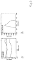
- FIGS. 2A and 2B show the simulated wall course in a 20 nm GaN / 20 nm InGaN / GaN buffer system and the charge carrier distribution. For this simulation, all layers are undoped and the indium content is 20%.
- Figs. 3A and 3B show the simulated wall trace and the carrier distribution in a GaN / InGaN / GaN system with an N-compensation charge in the InGaN channel as in Fig. 1B.
- a 10 nm thick N-compensation doping (1.5 x 10 19 cm -3 ) in the InGaN channel was assumed.
- FIGS. 4A and 4B show a corresponding simulation of a system as in FIG. 1C, ie with a 10 nm thick N compensation doping (1 ⁇ 10 19 cm -3 ) as a donor layer in the GaN buffer below the channel. In both cases of Figs. 3 and 4, the doping was chosen exactly so that the hole channel was compensated.
- FIG. 5 shows the layer structure of an inverted donor-doped GaN / InGaN / GaN field-effect transistor according to the present invention.
- the field effect transistor was applied to a sapphire substrate and additionally provided with contact electrodes 7, 8 and a gate electrode 9 (gate electrode).
- the indium content is approximately 7% in the 10 nm undoped InGaN layer of channel 2 and in the 10 nm thick doped InGaN: Si layer 4, 2.
- the 3 ⁇ m thick buffer 1 and the 20 nm thick cap layer 3 are each undoped.
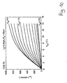
- FIG. 6 shows the output characteristic of this FET structure with 20 nm GaN undoped as a cap layer, 10 nm InGaN undoped as a channel, 10 nm InGaN doped (2 ⁇ 10 18 cm -3 ) as a compensation layer with an indium content of 7% and one 3 ⁇ m thick GaN buffer layer, which is also undoped.
- the gate length was chosen to be 0.5 ⁇ m. In this case, a maximum saturation current of 250 mA / mm has now been achieved.
- FIG. 8 shows the layer structure of an inverted InGaN-based donor-donor HEMT which has also been realized.
- the donor doping of 1 ⁇ 10 19 cm -3 is located in a 10 nm thick GaN layer 4 below the InGaN channel 2, separated therefrom by a 5 nm thick undoped GaN spacer layer 21 for the separation of the doping fuselages.
- the indium content in the 20 nm undoped InGaN layer 2 is 10%.
- the 3 ⁇ m thick GaN buffer 1 and the 20 nm thick GaN cap layer 3 are undoped.
- FIGS. 9 and 10 show the output characteristics of this structure. In the case of a transistor with a 0.5 ⁇ m gate length (FIG. 9) or with a 0.25 ⁇ m gate length (FIG. 10), a maximum saturation current of 600 mA / mm or 900 mA / mm was achieved.
- a free electron channel is formed by donor compensation doping of the vacant holes in an InGaN-based inverted HEMT structure.
- Fig. 11 the structure of such an inverter having an N-channel and a P-channel is InGaN-based HFET shown.
- the same reference numerals have been used for the same layers, wherein in the P-channel system, the corresponding reference numerals are shown as primed reference numerals (eg, 3 'instead of 3 for the cap layer).
- the layer structure of the N-channel transistor is in accordance with FIG. 8.
- the P-channel transistor consists of a 3 ⁇ m thick undoped GaN buffer 1, which the P-channel transistor has in common with the N-channel transistor , a 20 nm thick undoped InGaN layer 2 'with 10% indium content as a channel, a 5 nm thick magnesium-doped GaN layer for compensation doping of this induced electron channel with an acceptor concentration of 2 x 10 19 cm -3 and a 20 nm thick undoped GaN -Cap layer 3 '. Both in the N-type and in the P-type transistor, a space layer 21 or 21 'is located between the channel and the doped layer.
- an insulator 22 for example of SiO 2 or SiN, between the gates 9, 9 'and the semiconductor material of Cap layer 3, 3 'placed.
- FIG. 12 and FIG. 13 show the band profile or the charge carrier distribution of a P-channel InGaN-based heterostructure with N compensation doping as shown in the right-hand part of FIG. 11.
- a P-channel transistor is thus realized.
- Fig. 14 shows the DT output characteristic of such a P-channel HFET of 0.5 ⁇ m gate length.
Landscapes
- Junction Field-Effect Transistors (AREA)
- Surface Acoustic Wave Elements And Circuit Networks Thereof (AREA)
- Steroid Compounds (AREA)
- Insulated Gate Type Field-Effect Transistor (AREA)
- Crystals, And After-Treatments Of Crystals (AREA)
Description
- Die vorliegende Erfindung bezieht sich auf eine Heterostruktur wie sie beispielsweise für Feldeffektransistoren in der Leistungselektronik und Hochtemperaturelektronik eingesetzt werden. Dabei werden insbesondere Heterostrukturen, die einen In(Ga)N-Kanal, eine (Al)GaN-Cap-Schicht und eine GaN-Pufferschicht aufweisen, verwendet. Aufgrund der Materialeigenschaften von GaN und dessen Verbindungen wie AlGaN und InGaN werden diese Heterostrukturen in den letzten Jahren intensiv beforscht, um Anwendungen in der Leistungselektronik und Hochtemperaturelektronik zu ermöglichen.
- Bei Heterostrukturen, die einen In(Ga)N-Kanal, eine (Al)GaN-Cap-Schicht und eine GaN-Pufferschicht oder -Substrat aufweisen, ist der InGaN-Kanal aufgrund der unterschiedlichen Gitterkonstanten von GaN und InGaN verspannt. Materialbedingt entstehen dadurch im GaN/InGaN/GaN-System piezoelektrische Felder, die an den Grenzflächen polarisierte Ladungen (Piezoladungen) erzeugen. Eine GaN/InGaN/GaN-Heterostruktur besitzt dabei eine positive Grenzflächenladung am InGaN/GaN und eine negative Grenzflächenladung am GaN/InGaN-Übergang (Interface). Die erzeugten Grenzflächenladungen können bei einem Indiumgehalt von 100 % eine Ladungsträgerdichte von 1,3 x 1014 cm-2 erreichen. Der Vorteil dieser Struktur besteht darin, daß die durch die piezoelektrischen Felder erzeugten Ladungen sich im Kanal befinden. Aufgrund der Materialeigenschaften von GaN bilden sich zusätzlich spontane Polarisationsladungen an der Oberfläche und der Pufferrückseite, die jedoch nur einen sekundären Einfluß auf die Transistoreigenschaften haben.
- Piezoelektrische Felder in GaN/InGaN-Heterostrukturen spielen auch eine wesentliche Rolle, wenn diese Strukturen als strahlungsemitterende Halbleiterchips (Leuchtdiode) eingesetzt werden. In WO 00/21143 weist die aktive Schicht in einer solchen Heterostruktur eine Einfach- oder Mehrfach-Quantenwell-Struktur auf. Um den das Strahlungsverhalten solcher Halbleiterchips beinträchtigenden Einfluß den piezoelektrischen Feldern in den Quantenfilmen zu eliminieren, werden diese Felder durch Dotierung möglichst vollständig beseitigt.
- Fig. 1 zeigt in ihrem Teilbild 1A eine solche Heterostruktur mit einem Puffer 1, einem Kanal 2, einer Cap-Schicht 3 und den Grenzflächen 5 bzw. 6 zwischen den Schichten 1/2 bzw. den Schichten 2/3. Weiterhin sind die Piezoladungen dargestellt, wobei zu erkennen ist, daß die erzeugte positive Piezoladung sich an der Grenzfläche 5 befindet und die erzeugte negative Piezoladung sich an der Grenzfläche 6 befindet. Unter dem Einfluß eines angelegten äußeren elektrischen Feldes E bewegen sich nun die Piezoladungen entgegengesetzt gemäß den Pfeilen A und B.
- In der Literatur sind modulationsdotierte (MODFET), kanaldotierte und undotierte (Piezo-FET) AlGaN/GaN-Feldeffektransistoren bekannt. Auch im AlGaN/GaN-System führen Verspannungen zu piezoelektrischen Feldern, die an den Grenzflächen polarisierten Ladungen bilden. Im Gegensatz zu einem GaN/InGaN/GaN-System befinden sich nicht beide Grenzflächenladungen im Kanal, sondern die negative Ladung am AlGaN/GaN-In terface als 2DEG (2-diversivales Elektronengas) und die positive Ladung an der AlGaN-Oberfläche.
- Der Nachteil einer solchen Struktur ist, daß die gebundene Grenzflächenladung an der AlGaN/GaN-Grenzfläche mit der gegenpoligen Oberflächenladung durch die polarisierenden Felder in Wechselwirkung zueinanderstehen. Die Oberflächenladungen nehmen im DC-Betrieb eines GaN-basierenden Transistors wenig Einfluß auf die Ausgangscharakteristik. Im RF-Betrieb muß die Ladung an der Oberfläche der Kanalladung aufgrund ihrer Wechselwirkung folgen. Vorausgesetzt die Ladungen im Kanal bewegen sich mit höherer Geschwindigkeit als die Oberflächenladung, so folgt bei einer charakteristischen Frequenz im RF-Betrieb die Oberflächenladung nicht mehr der Kanalladung. Diese jetzt gegenpolige quasi ortsfeste Ladung verletzt die Neutralitätsbedingung und kann nun die freien Ladungen im Kanal einfangen, mit der Konsequenz, daß der Ausgangsstrom abnimmt und die maximale RF-Leistung sich gegenüber der DC-Leistung reduziert.
- Im Gegensatz zum AlGaN/GaN-System befindet sich im GaN/InGaN/GaN-System keine durch die piezoelektrische Polarisation erzeugte Grenzflächenladung an der Probenoberfläche. Eine Wechselwirkung zwischen piezoelektrischer Polarisationsladung und Oberflächenladung wird vermieden. Dadurch wird der Effekt der Stromkompensation und dem resultierenden Leistungsabfall bei höherfrequenter Eingangsleistung, der bei AlGaN/GaN-Transistoren zu beobachten ist, verhindert.
- In einer GaN/InGaN/GaN tragen zum Stromtransport die positive Grenzflächenladung am rückseitigen InGaN/GaN-Interface und die induzierte negative Grenzflächenladung am GaN/InGaN vorderseitigen Interface bei. Im Vergleich zu GaN oder AlGaN ist die Elektronenbeweglichkeit in InGaN wesentlich höher und kann nach theoretischen Berechnungen 4500cm2/Vsec betragen. Die Beweglichkeit von Löchern ist im InGaN allerdings um ein Vielfaches geringer als die Elektronenbeweglichkeit. Der resultierende Nettostromfluß gegeben durch die positive Grenzflächenladung und negative Grenzflächenladung, ist bestimmt durch die Bedingung der Ladungsneutralität, d. h. der langsamere Löcherstrom bestimmt die resultierende Grenzfrequenz des Bauelements. Zudem kann der Kanal durch einen pn-Übergang gesperrt werden.
- Aufgabe der vorliegenden Erfindung ist es nun, die oben beschriebenen Nachteile bei Heterostrukturen mit einem Kanal aus einem piezopolaren Material zu vermeiden.
- Diese Aufgabe wird durch die Heterostruktur gemäß Patentanspruch 1 und dem Feldeffektransistor gemäß Patentanspruch 24 sowie die Verwendung gemäß Patentanspruch 28 gelöst. Vorteilhafte Weiterbildungen der Heterostruktur bzw. des Feldeffektransistors werden in den jeweiligen abhängigen Ansprüchen gegeben.
- Erfindungsgemäß werden beispielsweise durch eine dünne n-Dotierung im Kanal oder im Puffer bzw. Substrat die positive Polarisationsladung an der Grenzfläche zwischen Puffer und Kanal kompensiert, so daß nur ein Elektronenkanal resultiert. Dies ist mit Bezug auf die Figuren 1B sowie 1C dargestellt. 1B zeigt, wie durch die Dotierung mit einem ortsfesten Donator 12 bewegliche Elektronen 13 in den Kanal eingebracht werden, die mit der Piezoladung 10 rekombinieren, so daß lediglich noch die Elektronen 11 als bewegliche Ladungsträger im Kanal verbleiben.
- Die Fig. 1B zeigt die Verteilung der Ladung an einer invertierten GaN/InGaN/GaN HEMT-Struktur mit Donatordotierung im InGaN. Die Fig. 1C zeigt eine weitere Möglichkeit, nämlich die Verteilung der Ladung an einer invertierten GaN/InGaN/GaN HEMT-Struktur mit Donatordotierung im Puffer GaN. Deutlich zu sehen ist hier in gleicher Weise wie in Fig. 1B die Kompensation der positiven Piezoladung 10 im Kanal durch die Elektronenmodulationsdotierung aus der Spenderschicht 4, die ein dotierter Bereich des Puffers 1 ist. Als positive Gegenladung zur Elektronenkanalladung bleibt nach Rekombination der Ladung 10 und 13 lediglich eine positive ortsfeste Donatorladung 12 in der dotierten Spenderschicht 4 des Puffers 1 übrig. Fig. 2A und Fig. 2B zeigen den simulierten Wandverlauf in einem 20 nm GaN/20 nm InGaN/GaN-Puffersystem und die Ladungsträgerverteilung. Für diese Simulation sind alle Schichten undotiert und der Indiumgehalt beträgt 20 %. Demgegenüber zeigt Fig. 3A und 3B den simulierten Wandverlauf und die Ladungsträgerverteilung in einem GaN/InGaN/GaN-System mit einer N-Kompensationsladung im InGaN-Kanal wie in Fig. 1B. Für diese Simulation wurde eine 10 nm dicke N-Kompensationsdotierung (1,5 x 1019 cm-3) im InGaN-Kanal angenommen.
- Fig. 4A und Fig. 4B zeigen eine entsprechende Simulation eines Systems wie in Fig. 1C, d.h. mit einer 10 nm dicken N-Kompensationsdotierung (1 x 1019 cm-3) als Spenderschicht im GaN-Puffer unterhalb des Kanals. In beiden Fällen der Fig. 3 und 4 wurde die Dotierung exakt so gewählt, daß der Löcherkanal kompensiert wurde.
- Aus Fig. 3B und Fig. 4B ist im Vergleich zu Fig. 2B unmittelbar zu erkennen, daß die positiven Piezoladungen an der Grenzfläche zwischen Puffer und Kanal vollständig kompensiert wurden und folglich keine Löcherleitung im Kanal mehr vorliegt.
- Fig. 5 zeigt den Schichtaufbau eines invertierten GaN/InGaN/GaN-Feldeffektransistors mit rückseitiger Donatordotierung gemäß der vorliegenden Erfindung. Hier erfolgte die Dotierung mit Silizium als ortsfestem Donator (2 x 1018 cm-3) in einer 10 nm dicken InGaN-Schicht, die an der Grenzfläche zwischen dem Kanal 2 und dem Puffer 1 liegt. Der Feldeffektransistor wurde auf ein Substrat aus Saphir aufgebracht und zusätzlich mit Kontaktelektroden 7, 8 und einer Torelektrode 9 (Gate-Elektrode) versehen.
- Der Indiumgehalt beträgt in der 10 nm undotierten InGaN-Schicht des Kanals 2 und in der 10 nm dicken dotierten InGaN:Si-Schicht 4, 2 ca. 7 %. Der 3 µm dicke Puffer 1 und die 20 nm dicke Cap-Schicht 3 sind jeweils undotiert.
- Fig. 6 zeigt die Ausgangskennlinie dieser FET-Struktur mit 20 nm GaN undotiert als Cap-Schicht, 10 nm InGaN undotiert als Kanal, 10 nm InGaN dotiert (2 x 1018 cm-3) als Kompensationsschicht mit einem Indiumgehalt von 7 % und einer 3 µm dicken GaN-Pufferschicht, die ebenfalls undotiert ist. Die Gate-Länge. Die Gate-Länge wurde zu 0,5 µm gewählt. Hierbei wurde nun ein maximaler Sättigungsstrom von 250 mA/mm erreicht.
- Im abgeschnürten Zustand wurde mit einem derartigen FET eine Durchbruchspannung von 120 V erreicht. Das ergab eine Ausgangsleistung von 2,5 W/mm. Im RF-Betrieb konnte mit einer Eingangsleistung von 16 dBm an einer 50 Ohm Lastgerade bis 10 kHz keine Stromkompression festgestellt werden. Dies ist in Fig. 7 dargestellt, die den maximalen RF-Ausgangsstrom normiert auf den maximalen DC-Ausgangsstrom in Abhängigkeit von der Frequenz bei diesem FET aus Fig. 5 zeigt.
- Fig. 8 zeigt den Schichtaufbau eines invertierten InGaN-basierenden HEMT mit rückseitiger Donatordotierung, der ebenfalls realisiert wurde.
- Die Donatordotierung von 1 x 1019 cm-3 befindet sich in einer 10 nm dicken GaN-Schicht 4 unterhalb des InGaN-Kanals 2, von diesem getrennt durch eine 5 nm dicke undotierte GaN-Spacerschicht 21 zur Trennung der Dotierrümpfe. Der Indiumgehalt beträgt in der 20 nm undotierten InGaN-Schicht 2 10 %. Der 3 µm dikke GaN-Puffer 1 und die 20 nm dicke GaN-Cap-Schicht 3 sind undotiert. In den Fig. 9 und 10 sind die Ausgangskennlinien dieser Struktur dargestellt. Bei einem Transistor mit 0,5 µm Gate-Länge (Fig. 9) bzw. mit 0,25 µm Gate-Länge (Fig. 10) wurde ein maximaler Sättigungsstrom von 600 mA/mm bzw. 900 mA/mm erreicht.
- Mit den bisherigen Beispielen, die im wesentlichen Fig. 1B bzw. 1C entsprachen, wurde dargestellt, daß durch eine Donatorkompensationsdotierung der freien Löcher in einem InGaN-basierenden invertierten HEMT-Struktur ein freier Elektronenkanal entsteht. Es ist jedoch prinzipiell auch möglich, eine Akzeptor-Kompensationsdotierung der freien Elektronen durchzuführen und so einen freien Löcherkanal zu erzeugen. Dies ermöglicht es, komplementäre Logikschaltungen aufzubauen (in Analogie zur CMOS-Schaltung). In Fig. 11 ist der Aufbau eines derartigen Inverters mit einem N-Kanal und einem P-Kanal aus InGaN-basierten HFET dargestellt. Dabei wurden für die selben Schichten dieselben Bezugszeichen verwendet, wobei in dem P-Kanal-System die entsprechenden Bezugszeichen als gestrichene Bezugszeichen dargestellt werden (z.B. 3' statt 3 für die Cap-Schicht). Der Schichtaufbau des N-Kanal-Transistors ist dabei entsprechend Fig. 8. Der P-Kanal-Transistor besteht aus einem 3 µm dicken undotierten GaN-Puffer 1, den der P-Kanal-Transistor mit dem N-Kanal-Transistor in gemein hat, einer 20 nm dicken undotierten InGaN-Schicht 2' mit 10 % Indiumgehalt als Kanal, einer 5 nm dicken magnesiumdotierten GaN-Schicht zur Kompensationsdotierung des hierzu induzierten Elektronenkanals mit einer Akzeptorkonzentration von 2 x 1019 cm-3 sowie einer 20 nm dicken undotierten GaN-Cap-Schicht 3'. Sowohl im N-Typ als auch im P-Typ-Transistor befindet sich zwischen dem Kanal und der dotierten Schicht eine Space-Schicht 21 bzw. 21'.
- Zur Angleichung der beiden Potentiale des N-Typ-Transistors bzw. des P-Typ-Transistors unter dem Gate-Bereich der beiden Transistoren wird ein Isolator 22, beispielsweise aus SiO2 oder SiN, zwischen den Gates 9, 9' und dem Halbleitermaterial der Cap-Schicht 3, 3' plaziert.
- Fig. 12 und Fig. 13 zeigen den Bandverlauf bzw. die Ladungsträgerverteilung einer wie im rechten Teilbild der Figur 11 aufgebaut dargestellten P-Kanal InGaN-basierenden Heterostruktur mit N-Kompensationsdotierung. Bei Anlegen einer negativen Grain-Source-Spannung und einer positiven Gate-Spannung wird damit ein P-Kanal-Transistor realisiert. Dies wird in Fig. 14 dargestellt, in der die DT-Ausgangskennlinie eines derartigen P-Kanal-HFET mit 0,5 µm Gate-Länge dargestellt ist.
Claims (28)
- Heterostruktur mit einer Pufferschicht bzw. Substrat, einem auf der Pufferschicht bzw. dem Substrat angeordneten Kanal sowie einer auf dem Kanal angeordneten Cap-Schicht, wobei der Kanal aus einem piezopolaren Material besteht so daß sowohl an der Grenzfläche zwischen Pufferschicht bzw. Substrat und Kanal sowie an der Grenzfläche zwischen Kanal und Cap-Schicht Piezoladungen jeweils unterschiedlichen Ladungstyps entstehen,
dadurch gekennzeichnet, daß
entweder der Bereich um die Grenzfläche zwischen Pufferschicht bzw. Substrat und Kanal oder der Bereich um die Grenzfläche zwischen Kanal und Cap-Schicht derart dotiert ist, daß die an der jeweiligen Grenzfläche auftretenden Piezoladungen kompensiert werden. - Heterostruktur nach dem vorhergehenden Anspruch, gekennzeichnet durch eine GaN-Pufferschicht bzw. Substrat, einen auf der Pufferschicht bzw. dem- Substrat angeordneten InGaN-Kanal sowie eine auf dem Kanal angeordnete GaN- oder AlGaN-Cap-Schicht, wobei entweder der Bereich um die Grenzfläche zwischen Pufferschicht bzw. Substrat und Kanal n-dotiert ist oder
der Bereich um die Grenzfläche zwischen Kanal und Cap-Schicht p-dotiert ist. - Heterostruktur nach einem der vorhergehenden Ansprüche, dadurch gekennzeichnet, daß der Bereich um die Grenzfläche zwischen Pufferschicht bzw. Substrat und Kanal derart n-dotiert ist, daß die in dem Kanal vorhandenen piezoinduzierten positiven Ladungen kompensiert werden.
- Heterostruktur nach Anspruch 1 oder 2, dadurch gekennzeichnet, daß der Bereich um die Grenzfläche zwischen Kanal und Cap-Schicht derart p-dotiert ist, daß die in dem Kanal vorhandenen piezoinduzierten negativen Ladungen kompensiert werden.
- Heterostruktur nach einem der vorhergehenden Ansprüche, dadurch gekennzeichnet, daß der dotierte Bereich als Zwischenschicht zwischen Pufferschicht bzw. Substrat und Kanal bzw. zwischen Kanal und Cap-Schicht ausgebildet ist.
- Heterostruktur nach dem vorhergehenden Anspruch, dadurch gekennzeichnet, daß die Zwischenschicht eine GaN-Schicht oder InGaN-Schicht ist.
- Heterostruktur nach Anspruch 5, dadurch gekennzeichnet, daß die Zwischenschicht eine Zusammensetzung wie die entsprechende ihr benachbarte Pufferschicht bzw. Substrat, Kanal oder Cap-Schicht aufweist.
- Heterostruktur nach einem der vorhergehenden Ansprüche, dadurch gekennzeichnet, daß der dotierte Bereich bzw. die Zwischenschicht von dem Kanal durch eine undotierte Abstandschicht getrennt ist.
- Heterostruktur nach dem vorhergehenden Anspruch, dadurch gekennzeichnet, daß die Abstandschicht eine GaN-Schicht ist.
- Heterostruktur nach einem der Ansprüche 2 oder 6, dadurch gekennzeichnet, daß der Indiumgehalt in der InGaN-Schicht zwischen 1 % und 99 % je einschließlich beträgt.
- Heterostruktur nach dem vorhergehenden Anspruch, dadurch gekennzeichnet, daß der Indiumgehalt in der InGaN-Schicht zwischen 5 % und 30 % je einschließlich beträgt.
- Heterostruktur nach dem vorhergehenden Anspruch, dadurch gekennzeichnet, daß der Indiumgehalt in der InGaN-Schicht zwischen 7 % und 20 % je einschließlich beträgt.
- Heterostruktur nach dem vorhergehenden Anspruch, dadurch gekennzeichnet, daß der Indiumgehalt in der InGaN-Schicht 7 %, 10 % oder 20 % beträgt.
- Heterostruktur nach einem der vorhergehenden Ansprüche, dadurch gekennzeichnet, daß die Dicke der Pufferschicht bzw. des Substrats zwischen 1 und 10 µm, der Zwischenschicht zwischen 5 und 50 nm, der Abstandsschicht zwischen 1 und 20 nm, des Kanals zwischen 5 und
50 nm und/oder der Cap-Schicht zwischen 5 und 50 nm beträgt. - Heterostruktur nach dem vorhergehenden Anspruch, dadurch gekennzeichnet, daß die Dicke der Pufferschicht bzw. des Substrats etwa 3 µm, der Zwischenschicht etwa 10 nm, der Abstandschicht etwa 5 nm, des Kanals etwa
10 nm oder 20 nm und/oder der Cap-Schicht etwa 20 nm beträgt. - Heterostruktur nach einem der vorhergehenden Ansprüche, dadurch gekennzeichnet, daß der Bereich um die Grenzfläche zwischen der Pufferschicht bzw. dem Substrat und dem Kanal eine Donatordotierung zwischen 1 · 1018 cm-3 und 2 · 1019 cm-3 aufweist.
- Heterostruktur nach dem vorhergehenden Anspruch, dadurch gekennzeichnet, daß der Bereich um die Grenzfläche zwischen der Pufferschicht bzw. dem Substrat und dem Kanal eine Donatordotierung zwischen 2 · 1018 cm-3 und 1 · 1019 cm-3 je einschließlich aufweist.
- Heterostruktur nach Anspruch 16, dadurch gekennzeichnet, daß der Bereich um die Grenzfläche zwischen der Pufferschicht bzw. dem Substrat und dem Kanal eine Donatordotierung von 1 · 1018 cm-3 oder 2 · 1019 cm-3 aufweist.
- Heterostruktur nach einem der vorhergehenden Ansprüche, dadurch gekennzeichnet, daß der Dotierstoff für die Dotierung im Bereich um die Grenzfläche zwischen der Pufferschicht bzw. dem Substrat und dem Kanal Silizium ist.
- Heterostruktur nach einem der vorhergehenden Ansprüche, dadurch gekennzeichnet, daß der Bereich um die Grenzfläche zwischen Kanal und Cap-Schicht eine Akzeptordotierung zwischen 1 · 1018 cm-3 und 5 · 1019 cm-3 aufweist.
- Heterostruktur nach dem vorhergehenden Anspruch, dadurch gekennzeichnet, daß der Bereich um die Grenzfläche zwischen Kanal und Cap-Schicht eine Akzeptordotierung zwischen 2· 1018 cm-3 und 2 · 1019 cm-3 je einschließlich aufweist.
- Heterostruktur nach dem vorhergehenden Anspruch, dadurch gekennzeichnet, daß der Bereich um die Grenzfläche zwischen Kanal und Cap-Schicht eine Akzeptordotierung von 2 · 1019 cm-3 aufweist.
- Heterostruktur nach einem der vorhergehenden Ansprüche, dadurch gekennzeichnet, daß der Dotierstoff für die Dotierung im Bereich um die Grenzfläche zwischen Kanal und Cap-Schicht Magnesium ist.
- Feldeffekttransistor mit einer Heterostruktur nach einem der vorhergehenden Ansprüchen, dadurch gekennzeichnet, daß auf der dem Kanal abgewandten Oberfläche der Cap-Struktur zwei Kontaktelektroden und eine Torelektrode (Gateelektrode) angeordnet sind.
- Feldeffekttransistor nach dem vorhergehenden Anspruch, dadurch gekennzeichnet, daß die beiden Kontaktelektroden sperrfreie S- bzw. D-Kontakte sind.
- Feldeffekttransistor nach einem der Ansprüche 24 oder 25, dadurch gekennzeichnet, daß die Gateelektrode eine Schottky-Metall-Gateelektrode ist.
- Feldeffekttransistor nach einem der Ansprüche 24 bis 26, dadurch gekennzeichnet, daß die Gateelektrode einen p--dotierten Gatekontakt aufweist.
- Verwendung von Heterostrukturen und Feldeffekttransistoren nach einem der vorhergehenden Ansprüche für die Leistungselektronik oder Hochtemperaturelektronik, in Feldeffektransistoren oder Logikschaltungen, insbesondere komplementären Logikschaltungen.
Applications Claiming Priority (3)
| Application Number | Priority Date | Filing Date | Title |
|---|---|---|---|
| DE10027052 | 2000-06-02 | ||
| DE10027052 | 2000-06-02 | ||
| PCT/EP2001/006279 WO2001092428A1 (de) | 2000-06-02 | 2001-06-01 | Heterostruktur mit rückseitiger donatordotierung |
Publications (2)
| Publication Number | Publication Date |
|---|---|
| EP1292648A2 EP1292648A2 (de) | 2003-03-19 |
| EP1292648B1 true EP1292648B1 (de) | 2007-04-11 |
Family
ID=7644271
Family Applications (1)
| Application Number | Title | Priority Date | Filing Date |
|---|---|---|---|
| EP01964955A Expired - Lifetime EP1292648B1 (de) | 2000-06-02 | 2001-06-01 | Heterostruktur mit rückseitiger donatordotierung |
Country Status (7)
| Country | Link |
|---|---|
| US (2) | US7352008B2 (de) |
| EP (1) | EP1292648B1 (de) |
| JP (1) | JP5179694B2 (de) |
| AT (1) | ATE359602T1 (de) |
| AU (1) | AU2001285729A1 (de) |
| DE (1) | DE50112334D1 (de) |
| WO (1) | WO2001092428A1 (de) |
Families Citing this family (19)
| Publication number | Priority date | Publication date | Assignee | Title |
|---|---|---|---|---|
| DE50112334D1 (de) * | 2000-06-02 | 2007-05-24 | Microgan Gmbh | Heterostruktur mit rückseitiger donatordotierung |
| DE50211972D1 (de) * | 2001-07-20 | 2008-05-08 | Erhard Kohn | Feldeffekttransistor |
| JP2004006461A (ja) * | 2002-05-31 | 2004-01-08 | Nec Corp | 半導体装置 |
| US7928455B2 (en) * | 2002-07-15 | 2011-04-19 | Epistar Corporation | Semiconductor light-emitting device and method for forming the same |
| US7700973B2 (en) * | 2003-10-10 | 2010-04-20 | The Regents Of The University Of California | GaN/AlGaN/GaN dispersion-free high electron mobility transistors |
| US7268375B2 (en) * | 2003-10-27 | 2007-09-11 | Sensor Electronic Technology, Inc. | Inverted nitride-based semiconductor structure |
| JP3931879B2 (ja) * | 2003-11-28 | 2007-06-20 | 株式会社デンソー | センサフュージョンシステム及びそれを用いた車両制御装置 |
| US7525130B2 (en) * | 2004-09-29 | 2009-04-28 | The Regents Of The University Of California | Polarization-doped field effect transistors (POLFETS) and materials and methods for making the same |
| US7615774B2 (en) | 2005-04-29 | 2009-11-10 | Cree.Inc. | Aluminum free group III-nitride based high electron mobility transistors |
| TW200830550A (en) * | 2006-08-18 | 2008-07-16 | Univ California | High breakdown enhancement mode gallium nitride based high electron mobility transistors with integrated slant field plate |
| JP4712683B2 (ja) * | 2006-12-21 | 2011-06-29 | パナソニック株式会社 | トランジスタおよびその製造方法 |
| WO2008151842A1 (de) * | 2007-06-15 | 2008-12-18 | Microgan Gmbh | Logikschaltung auf basis von nitriden von hauptgruppe-iii-elementen |
| JP4584293B2 (ja) | 2007-08-31 | 2010-11-17 | 富士通株式会社 | 窒化物半導体装置、ドハティ増幅器、ドレイン電圧制御増幅器 |
| GB0717802D0 (en) * | 2007-09-12 | 2007-10-24 | Photonstar Led Ltd | Electrically isolated vertical light emitting diode structure |
| KR101774933B1 (ko) * | 2010-03-02 | 2017-09-06 | 삼성전자 주식회사 | 듀얼 디플리션을 나타내는 고 전자 이동도 트랜지스터 및 그 제조방법 |
| JP2013041986A (ja) * | 2011-08-16 | 2013-02-28 | Advanced Power Device Research Association | GaN系半導体装置 |
| CN105556678B (zh) * | 2013-09-30 | 2018-04-10 | Hrl实验室有限责任公司 | 具有高阈值电压和低导通电阻的常关型iii族氮化物晶体管 |
| US11581866B2 (en) * | 2016-03-11 | 2023-02-14 | Akoustis, Inc. | RF acoustic wave resonators integrated with high electron mobility transistors including a shared piezoelectric/buffer layer and methods of forming the same |
| US11349023B2 (en) * | 2019-10-01 | 2022-05-31 | Taiwan Semiconductor Manufacturing Company, Ltd. | Integration of p-channel and n-channel E-FET III-V devices without parasitic channels |
Family Cites Families (36)
| Publication number | Priority date | Publication date | Assignee | Title |
|---|---|---|---|---|
| JPH0629574A (ja) * | 1992-03-10 | 1994-02-04 | Asahi Chem Ind Co Ltd | 発光素子およびその製造方法 |
| US5571732A (en) * | 1993-08-19 | 1996-11-05 | Texas Instruments Incorporated | Method for fabricating a bipolar transistor |
| JP3269344B2 (ja) * | 1995-08-21 | 2002-03-25 | 松下電器産業株式会社 | 結晶成長方法および半導体発光素子 |
| JP3307218B2 (ja) * | 1996-03-11 | 2002-07-24 | 日亜化学工業株式会社 | 窒化物半導体レーザ素子の製造方法 |
| JPH09266352A (ja) * | 1996-03-28 | 1997-10-07 | Fuji Photo Film Co Ltd | 半導体発光素子 |
| JP3478005B2 (ja) * | 1996-06-10 | 2003-12-10 | ソニー株式会社 | 窒化物系化合物半導体のエッチング方法および半導体装置の製造方法 |
| JP3458625B2 (ja) * | 1996-11-13 | 2003-10-20 | ソニー株式会社 | 半導体の成長方法 |
| US5929467A (en) * | 1996-12-04 | 1999-07-27 | Sony Corporation | Field effect transistor with nitride compound |
| JPH10189944A (ja) * | 1996-12-24 | 1998-07-21 | Furukawa Electric Co Ltd:The | 高電子移動度トランジスタ |
| JPH10294452A (ja) * | 1997-04-22 | 1998-11-04 | Sony Corp | ヘテロ接合電界効果トランジスタ |
| US6784463B2 (en) * | 1997-06-03 | 2004-08-31 | Lumileds Lighting U.S., Llc | III-Phospide and III-Arsenide flip chip light-emitting devices |
| US5926726A (en) * | 1997-09-12 | 1999-07-20 | Sdl, Inc. | In-situ acceptor activation in group III-v nitride compound semiconductors |
| JPH11261053A (ja) * | 1998-03-09 | 1999-09-24 | Furukawa Electric Co Ltd:The | 高移動度トランジスタ |
| JP3369464B2 (ja) * | 1998-03-19 | 2003-01-20 | 日本電信電話株式会社 | 半導体装置 |
| US6064078A (en) * | 1998-05-22 | 2000-05-16 | Xerox Corporation | Formation of group III-V nitride films on sapphire substrates with reduced dislocation densities |
| US6657300B2 (en) * | 1998-06-05 | 2003-12-02 | Lumileds Lighting U.S., Llc | Formation of ohmic contacts in III-nitride light emitting devices |
| JP3642199B2 (ja) * | 1998-09-22 | 2005-04-27 | 松下電器産業株式会社 | 窒化ガリウム系化合物半導体発光素子の製造方法 |
| WO2000021143A1 (de) * | 1998-10-05 | 2000-04-13 | Osram Opto Semiconductors Gmbh & Co. Ohg | Strahlungsemittierender halbleiterchip |
| JP3209270B2 (ja) * | 1999-01-29 | 2001-09-17 | 日本電気株式会社 | ヘテロ接合電界効果トランジスタ |
| GB9912583D0 (en) * | 1999-05-28 | 1999-07-28 | Arima Optoelectronics Corp | A light emitting diode having a two well system with asymmetric tunneling |
| US6592663B1 (en) * | 1999-06-09 | 2003-07-15 | Ricoh Company Ltd. | Production of a GaN bulk crystal substrate and a semiconductor device formed on a GaN bulk crystal substrate |
| US6567443B2 (en) * | 1999-09-29 | 2003-05-20 | Xerox Corporation | Structure and method for self-aligned, index-guided, buried heterostructure AlGalnN laser diodes |
| US6441393B2 (en) * | 1999-11-17 | 2002-08-27 | Lumileds Lighting U.S., Llc | Semiconductor devices with selectively doped III-V nitride layers |
| US6515313B1 (en) * | 1999-12-02 | 2003-02-04 | Cree Lighting Company | High efficiency light emitters with reduced polarization-induced charges |
| US6803596B2 (en) * | 1999-12-27 | 2004-10-12 | Sanyo Electric Co., Ltd. | Light emitting device |
| JP3393602B2 (ja) * | 2000-01-13 | 2003-04-07 | 松下電器産業株式会社 | 半導体装置 |
| DE50112334D1 (de) * | 2000-06-02 | 2007-05-24 | Microgan Gmbh | Heterostruktur mit rückseitiger donatordotierung |
| US6727531B1 (en) * | 2000-08-07 | 2004-04-27 | Advanced Technology Materials, Inc. | Indium gallium nitride channel high electron mobility transistors, and method of making the same |
| JP2002064201A (ja) * | 2000-08-18 | 2002-02-28 | Toshiba Corp | 半導体電界効果トランジスタ及び電力増幅器 |
| US6548333B2 (en) * | 2000-12-01 | 2003-04-15 | Cree, Inc. | Aluminum gallium nitride/gallium nitride high electron mobility transistors having a gate contact on a gallium nitride based cap segment |
| US6630692B2 (en) * | 2001-05-29 | 2003-10-07 | Lumileds Lighting U.S., Llc | III-Nitride light emitting devices with low driving voltage |
| DE50211972D1 (de) * | 2001-07-20 | 2008-05-08 | Erhard Kohn | Feldeffekttransistor |
| US6515308B1 (en) * | 2001-12-21 | 2003-02-04 | Xerox Corporation | Nitride-based VCSEL or light emitting diode with p-n tunnel junction current injection |
| JP4385205B2 (ja) * | 2002-12-16 | 2009-12-16 | 日本電気株式会社 | 電界効果トランジスタ |
| US7268375B2 (en) * | 2003-10-27 | 2007-09-11 | Sensor Electronic Technology, Inc. | Inverted nitride-based semiconductor structure |
| JP2006269534A (ja) * | 2005-03-22 | 2006-10-05 | Eudyna Devices Inc | 半導体装置及びその製造方法、その半導体装置製造用基板及びその製造方法並びにその半導体成長用基板 |
-
2001
- 2001-06-01 DE DE50112334T patent/DE50112334D1/de not_active Expired - Lifetime
- 2001-06-01 WO PCT/EP2001/006279 patent/WO2001092428A1/de not_active Ceased
- 2001-06-01 AT AT01964955T patent/ATE359602T1/de active
- 2001-06-01 US US10/297,234 patent/US7352008B2/en not_active Expired - Lifetime
- 2001-06-01 JP JP2002500626A patent/JP5179694B2/ja not_active Expired - Fee Related
- 2001-06-01 AU AU2001285729A patent/AU2001285729A1/en not_active Abandoned
- 2001-06-01 EP EP01964955A patent/EP1292648B1/de not_active Expired - Lifetime
-
2006
- 2006-01-03 US US11/324,601 patent/US7394112B2/en not_active Expired - Fee Related
Also Published As
| Publication number | Publication date |
|---|---|
| WO2001092428A8 (de) | 2002-01-03 |
| US7352008B2 (en) | 2008-04-01 |
| AU2001285729A1 (en) | 2001-12-11 |
| US7394112B2 (en) | 2008-07-01 |
| JP5179694B2 (ja) | 2013-04-10 |
| EP1292648A2 (de) | 2003-03-19 |
| JP2003535481A (ja) | 2003-11-25 |
| ATE359602T1 (de) | 2007-05-15 |
| US20060113564A1 (en) | 2006-06-01 |
| DE50112334D1 (de) | 2007-05-24 |
| WO2001092428A3 (de) | 2002-05-30 |
| WO2001092428A1 (de) | 2001-12-06 |
| US20030155578A1 (en) | 2003-08-21 |
Similar Documents
| Publication | Publication Date | Title |
|---|---|---|
| DE102016119563B4 (de) | Bidirektionale selbstsperrende Bauelemente und Schaltungen | |
| EP1292648A2 (de) | Heterostruktur mit rückseitiger donatordotierung | |
| DE112012004541B4 (de) | Halbleitervorrichtung | |
| DE112014003481B4 (de) | GaN-TRANSISTOREN MIT POLYSILIZIUMSCHICHTEN ZUR BILDUNG VON ZUSÄTZLICHEN KOMPONENTEN UND VERFAHREN ZU DEREN HERSTELLUNG | |
| DE102016125865B4 (de) | Verfahren zum Herstellen eines Halbleiterbauelements und Halbleiterbauelement | |
| DE102004058431B4 (de) | III-Nitrid Halbleitervorrichtung mit Grabenstruktur | |
| DE102012107523B4 (de) | HEMT mit integrierter Diode mit niedriger Durchlassspannung | |
| DE102014108628B4 (de) | Kaskadendioden und Verfahren zur Herstellung einer Kaskadendiode | |
| DE102016114496A1 (de) | Lawinenrobuster quasi-vertikaler hemt | |
| DE102015119345B4 (de) | Halbleiterfeldplatte für verbindungshalbleiterbauelemente | |
| DE102016113735A1 (de) | Durchschlagfestes HEMT-Substrat und Bauelement | |
| DE102014116091B4 (de) | Halbleiterbauelement | |
| DE102016101909A1 (de) | Schaltkreis und Halbleiterbauelement | |
| DE102013112831B4 (de) | Ladungskompensations-Halbleiterbauelement | |
| DE102013003283A1 (de) | Selbstsperrender verbundhalbleiter-tunneltransistor | |
| DE102014108625A1 (de) | Gate-stack für selbstsperrenden verbundhalbleitertransistor | |
| DE102014109147A1 (de) | Feldeffekthalbleiter-Bauelement sowie Verfahren zu dessen Betrieb und Herstellung | |
| DE102012101217A1 (de) | Normalerweise ausgeschaltete Halbleiterschalter und normalerweise ausgeschaltete JFETs | |
| DE102013102457A1 (de) | Überspannungsschutzeinrichtung für verbindungshalbleiter-feldeffekttransistoren | |
| DE102014102467A1 (de) | Ladungsschutz für III-Nitrid-Vorrichtungen | |
| DE102014118834A1 (de) | Halbleiterbauelement und Verfahren | |
| DE112022003273T5 (de) | Schaltungen und Verfahren zur Steuerung einer Spannung eines Halbleitersubstrats | |
| DE102015100388A1 (de) | Anreicherungstyp-Bauelement | |
| DE102016106314A1 (de) | Integrierte halbleitervorrichtung | |
| DE102008008931B3 (de) | Vorrichtung und Verfahren zum Schalten von elektrischen Signalen und Leistungen |
Legal Events
| Date | Code | Title | Description |
|---|---|---|---|
| PUAI | Public reference made under article 153(3) epc to a published international application that has entered the european phase |
Free format text: ORIGINAL CODE: 0009012 |
|
| 17P | Request for examination filed |
Effective date: 20021213 |
|
| AK | Designated contracting states |
Kind code of ref document: A2 Designated state(s): AT BE CH CY DE DK ES FI FR GB GR IE IT LI LU MC NL PT SE TR |
|
| AX | Request for extension of the european patent |
Extension state: AL LT LV MK RO SI |
|
| RIN1 | Information on inventor provided before grant (corrected) |
Inventor name: KAMP, MARKUS Inventor name: SEYBOTH, MATTHIAS Inventor name: DAUMILLER, INGO Inventor name: KOHN, ERHARD |
|
| RAP1 | Party data changed (applicant data changed or rights of an application transferred) |
Owner name: MICROGAN GMBH |
|
| GRAP | Despatch of communication of intention to grant a patent |
Free format text: ORIGINAL CODE: EPIDOSNIGR1 |
|
| RIC1 | Information provided on ipc code assigned before grant |
Ipc: H01L 29/36 20060101AFI20060718BHEP Ipc: H01L 29/778 20060101ALI20060718BHEP |
|
| GRAS | Grant fee paid |
Free format text: ORIGINAL CODE: EPIDOSNIGR3 |
|
| GRAA | (expected) grant |
Free format text: ORIGINAL CODE: 0009210 |
|
| AK | Designated contracting states |
Kind code of ref document: B1 Designated state(s): AT BE CH CY DE DK ES FI FR GB GR IE IT LI LU MC NL PT SE TR |
|
| PG25 | Lapsed in a contracting state [announced via postgrant information from national office to epo] |
Ref country code: FI Free format text: LAPSE BECAUSE OF FAILURE TO SUBMIT A TRANSLATION OF THE DESCRIPTION OR TO PAY THE FEE WITHIN THE PRESCRIBED TIME-LIMIT Effective date: 20070411 |
|
| REG | Reference to a national code |
Ref country code: GB Ref legal event code: FG4D Free format text: NOT ENGLISH |
|
| REG | Reference to a national code |
Ref country code: CH Ref legal event code: NV Representative=s name: TROESCH SCHEIDEGGER WERNER AG Ref country code: CH Ref legal event code: EP |
|
| GBT | Gb: translation of ep patent filed (gb section 77(6)(a)/1977) |
Effective date: 20070411 |
|
| REG | Reference to a national code |
Ref country code: IE Ref legal event code: FG4D Free format text: LANGUAGE OF EP DOCUMENT: GERMAN |
|
| REF | Corresponds to: |
Ref document number: 50112334 Country of ref document: DE Date of ref document: 20070524 Kind code of ref document: P |
|
| PG25 | Lapsed in a contracting state [announced via postgrant information from national office to epo] |
Ref country code: ES Free format text: LAPSE BECAUSE OF FAILURE TO SUBMIT A TRANSLATION OF THE DESCRIPTION OR TO PAY THE FEE WITHIN THE PRESCRIBED TIME-LIMIT Effective date: 20070722 |
|
| REG | Reference to a national code |
Ref country code: SE Ref legal event code: TRGR |
|
| PG25 | Lapsed in a contracting state [announced via postgrant information from national office to epo] |
Ref country code: PT Free format text: LAPSE BECAUSE OF FAILURE TO SUBMIT A TRANSLATION OF THE DESCRIPTION OR TO PAY THE FEE WITHIN THE PRESCRIBED TIME-LIMIT Effective date: 20070911 |
|
| ET | Fr: translation filed | ||
| NLV1 | Nl: lapsed or annulled due to failure to fulfill the requirements of art. 29p and 29m of the patents act | ||
| REG | Reference to a national code |
Ref country code: IE Ref legal event code: FD4D |
|
| BERE | Be: lapsed |
Owner name: MICROGAN G.M.B.H. Effective date: 20070630 |
|
| PG25 | Lapsed in a contracting state [announced via postgrant information from national office to epo] |
Ref country code: IE Free format text: LAPSE BECAUSE OF FAILURE TO SUBMIT A TRANSLATION OF THE DESCRIPTION OR TO PAY THE FEE WITHIN THE PRESCRIBED TIME-LIMIT Effective date: 20070411 Ref country code: NL Free format text: LAPSE BECAUSE OF FAILURE TO SUBMIT A TRANSLATION OF THE DESCRIPTION OR TO PAY THE FEE WITHIN THE PRESCRIBED TIME-LIMIT Effective date: 20070411 Ref country code: MC Free format text: LAPSE BECAUSE OF NON-PAYMENT OF DUE FEES Effective date: 20070630 Ref country code: DK Free format text: LAPSE BECAUSE OF FAILURE TO SUBMIT A TRANSLATION OF THE DESCRIPTION OR TO PAY THE FEE WITHIN THE PRESCRIBED TIME-LIMIT Effective date: 20070411 |
|
| PLBE | No opposition filed within time limit |
Free format text: ORIGINAL CODE: 0009261 |
|
| STAA | Information on the status of an ep patent application or granted ep patent |
Free format text: STATUS: NO OPPOSITION FILED WITHIN TIME LIMIT |
|
| 26N | No opposition filed |
Effective date: 20080114 |
|
| PG25 | Lapsed in a contracting state [announced via postgrant information from national office to epo] |
Ref country code: BE Free format text: LAPSE BECAUSE OF NON-PAYMENT OF DUE FEES Effective date: 20070630 |
|
| PG25 | Lapsed in a contracting state [announced via postgrant information from national office to epo] |
Ref country code: GR Free format text: LAPSE BECAUSE OF FAILURE TO SUBMIT A TRANSLATION OF THE DESCRIPTION OR TO PAY THE FEE WITHIN THE PRESCRIBED TIME-LIMIT Effective date: 20070712 |
|
| PG25 | Lapsed in a contracting state [announced via postgrant information from national office to epo] |
Ref country code: CY Free format text: LAPSE BECAUSE OF FAILURE TO SUBMIT A TRANSLATION OF THE DESCRIPTION OR TO PAY THE FEE WITHIN THE PRESCRIBED TIME-LIMIT Effective date: 20070411 |
|
| PG25 | Lapsed in a contracting state [announced via postgrant information from national office to epo] |
Ref country code: LU Free format text: LAPSE BECAUSE OF NON-PAYMENT OF DUE FEES Effective date: 20070601 |
|
| PG25 | Lapsed in a contracting state [announced via postgrant information from national office to epo] |
Ref country code: TR Free format text: LAPSE BECAUSE OF FAILURE TO SUBMIT A TRANSLATION OF THE DESCRIPTION OR TO PAY THE FEE WITHIN THE PRESCRIBED TIME-LIMIT Effective date: 20070411 |
|
| REG | Reference to a national code |
Ref country code: DE Ref legal event code: R082 Ref document number: 50112334 Country of ref document: DE Representative=s name: WITTE, WELLER & PARTNER PATENTANWAELTE MBB, DE |
|
| REG | Reference to a national code |
Ref country code: FR Ref legal event code: PLFP Year of fee payment: 16 |
|
| REG | Reference to a national code |
Ref country code: FR Ref legal event code: PLFP Year of fee payment: 17 |
|
| REG | Reference to a national code |
Ref country code: FR Ref legal event code: PLFP Year of fee payment: 18 |
|
| PGFP | Annual fee paid to national office [announced via postgrant information from national office to epo] |
Ref country code: IT Payment date: 20190624 Year of fee payment: 19 |
|
| PGFP | Annual fee paid to national office [announced via postgrant information from national office to epo] |
Ref country code: SE Payment date: 20190619 Year of fee payment: 19 Ref country code: FR Payment date: 20190619 Year of fee payment: 19 |
|
| PGFP | Annual fee paid to national office [announced via postgrant information from national office to epo] |
Ref country code: CH Payment date: 20190619 Year of fee payment: 19 |
|
| PGFP | Annual fee paid to national office [announced via postgrant information from national office to epo] |
Ref country code: GB Payment date: 20190619 Year of fee payment: 19 Ref country code: AT Payment date: 20190621 Year of fee payment: 19 |
|
| PGFP | Annual fee paid to national office [announced via postgrant information from national office to epo] |
Ref country code: DE Payment date: 20200724 Year of fee payment: 20 |
|
| REG | Reference to a national code |
Ref country code: CH Ref legal event code: PL |
|
| REG | Reference to a national code |
Ref country code: AT Ref legal event code: MM01 Ref document number: 359602 Country of ref document: AT Kind code of ref document: T Effective date: 20200601 |
|
| GBPC | Gb: european patent ceased through non-payment of renewal fee |
Effective date: 20200601 |
|
| PG25 | Lapsed in a contracting state [announced via postgrant information from national office to epo] |
Ref country code: GB Free format text: LAPSE BECAUSE OF NON-PAYMENT OF DUE FEES Effective date: 20200601 Ref country code: FR Free format text: LAPSE BECAUSE OF NON-PAYMENT OF DUE FEES Effective date: 20200630 Ref country code: LI Free format text: LAPSE BECAUSE OF NON-PAYMENT OF DUE FEES Effective date: 20200630 Ref country code: CH Free format text: LAPSE BECAUSE OF NON-PAYMENT OF DUE FEES Effective date: 20200630 |
|
| PG25 | Lapsed in a contracting state [announced via postgrant information from national office to epo] |
Ref country code: AT Free format text: LAPSE BECAUSE OF NON-PAYMENT OF DUE FEES Effective date: 20200601 Ref country code: SE Free format text: LAPSE BECAUSE OF NON-PAYMENT OF DUE FEES Effective date: 20200602 |
|
| REG | Reference to a national code |
Ref country code: DE Ref legal event code: R071 Ref document number: 50112334 Country of ref document: DE |
|
| REG | Reference to a national code |
Ref country code: SE Ref legal event code: EUG |
|
| PG25 | Lapsed in a contracting state [announced via postgrant information from national office to epo] |
Ref country code: IT Free format text: LAPSE BECAUSE OF NON-PAYMENT OF DUE FEES Effective date: 20200601 |