EP1290561B1 - Multiple access per cycle in a multiple bank dimm - Google Patents
Multiple access per cycle in a multiple bank dimm Download PDFInfo
- Publication number
- EP1290561B1 EP1290561B1 EP01937381.0A EP01937381A EP1290561B1 EP 1290561 B1 EP1290561 B1 EP 1290561B1 EP 01937381 A EP01937381 A EP 01937381A EP 1290561 B1 EP1290561 B1 EP 1290561B1
- Authority
- EP
- European Patent Office
- Prior art keywords
- clock signal
- memory chip
- memory
- data
- clock
- Prior art date
- Legal status (The legal status is an assumption and is not a legal conclusion. Google has not performed a legal analysis and makes no representation as to the accuracy of the status listed.)
- Expired - Lifetime
Links
Images


Classifications
-
- G—PHYSICS
- G06—COMPUTING OR CALCULATING; COUNTING
- G06F—ELECTRIC DIGITAL DATA PROCESSING
- G06F13/00—Interconnection of, or transfer of information or other signals between, memories, input/output devices or central processing units
- G06F13/38—Information transfer, e.g. on bus
- G06F13/42—Bus transfer protocol, e.g. handshake; Synchronisation
- G06F13/4204—Bus transfer protocol, e.g. handshake; Synchronisation on a parallel bus
- G06F13/4234—Bus transfer protocol, e.g. handshake; Synchronisation on a parallel bus being a memory bus
- G06F13/4243—Bus transfer protocol, e.g. handshake; Synchronisation on a parallel bus being a memory bus with synchronous protocol
-
- G—PHYSICS
- G11—INFORMATION STORAGE
- G11C—STATIC STORES
- G11C7/00—Arrangements for writing information into, or reading information out from, a digital store
- G11C7/10—Input/output [I/O] data interface arrangements, e.g. I/O data control circuits, I/O data buffers
-
- G—PHYSICS
- G11—INFORMATION STORAGE
- G11C—STATIC STORES
- G11C7/00—Arrangements for writing information into, or reading information out from, a digital store
- G11C7/10—Input/output [I/O] data interface arrangements, e.g. I/O data control circuits, I/O data buffers
- G11C7/1015—Read-write modes for single port memories, i.e. having either a random port or a serial port
- G11C7/1042—Read-write modes for single port memories, i.e. having either a random port or a serial port using interleaving techniques, i.e. read-write of one part of the memory while preparing another part
Definitions
- the present invention relates to providing increased data access speed in computer memories without increasing the basic clock rate of the memory.
- Double Bus Rate means that the Data Rate out of and into a BUS system will be double of what each individual chip connected to the BUS delivers at its operating clock frequency.
- a memory chip of the single data rate type SDR operating at a certain base frequency will produce data rate DR of one period of the base frequency.
- a DR of 100 MHz means that the duration of each data bit will be equal to one period of the 100 MHz frequency which is equal to 10 nanoseconds.
- the data bit pulse- width coming out of the DRAM chip will be one period of the base clock. Therefore, as shown in figure 1 A , the actual frequency [MPW1] of any data bit alternating between 1 and 0 when the base clock is 100 MHz is 50 MHz.
- a cluster of memory chips such as SDRAMs
- SDRAMs are assembled together on a printed circuit board.
- the smallest bus-width is the actual number of bits coming out of a single SDRAM chip in a cluster of one).
- These boards are configured in several forms, known as SIMMs, DIMMs, SODIMMs, RIMMs, etc.
- SIMMs SIMMs
- DIMMs DIMMs
- SODIMMs SODIMMs
- RIMMs etc.
- DIMM will be used hereinafter to refer to any or all of these different types.
- the prior art DIMM module of 168 pins (the design applies to any DIMM of any other pin count, or any other package known by any other name), currently uses (as defined by the JEDEC 1 Committee) 72 Data bits bus, Control lines, Address lines, Power and Clocks.
- the present modules as defined by the JEDEC standard can accommodate up to two Banks or Rows of SDRAM chips. Other configurations of banks are also used depending on the system architecture. The selection of the Banks is controlled by a single Chip Select (CS) line or a combination of the Chip Selects and other control lines.
- the DIMM module is either a Register or Non-Register configuration. In a Register configuration all the Address and Control lines are latched into a Register first before they are presented to the devices to be selected for operation.
- Non-Register[MPW2] configuration the Address and Control lines are wired directly from the input tabs of the DIMM to the devices.
- Either configuration can have a Phase Locked Loop (PLL) for clock synchronization or utilize the clock presented to the DIMM by the system.
- PLL Phase Locked Loop
- the module can only produce a maximum DR of 100 MHz. If the clock frequency is raised to 133 MHz, and the SDRAM devices on the DIMM operate at 133 MHz, the maximum DR is increased to 133 MHz. In order to achieve 200 MHz DR, the SDRAM chips must operate at the base frequency of 200 MHz.
- FIG. 2 it is seen that, in the prior art, two identical memory chips 100, 102, are controlled by the same 100 MHz clock at clock input A 104, and clock input B 106.
- the single bit output 106 of chip A is connected to the corresponding output 107 of chip B. Only one chip is allowed to operate at any given time with the other chip isolated to high impedance by internal chip circuitry at the outputs 106, 107.
- the Chip Select (CS) input of Chip A 120 allows Chip A to access the data, and the corresponding input 121 does the same for chip B.
- This architecture is the basis for building DIMM modules with prior art.
- the data bit at pin D 106,107 will either come from chip A or chip B.
- the clock which appears at the input pin of chip A 104 and chip B 105 has a 100 MHZ frequency.
- a typical clock cycle begins at t1 with an positive-going signal, and ends at t2, 10 nanoseconds later.
- a typical data signal, shown as Figure 2C is synchronized with the clock signal, so that a data "one" condition begins at t1, and ends at t2, while the following data "zero" begins at t2 and ends at t3.
- the highest bandwidth data signal which be processed by this system is one with alternating ones and zeros. Still referring to figure 2C , it is seen that such a data signal has a frequency of one-half the clock frequency, although the data rate, measured in bits per second, is the same as the clock rate.
- the highest data rate DR delivered to a memory bus of the prior art system is equal to the data rate that the memory chips A or chips B can deliver by design.
- the JEDEC group has developed an architecture wherein one bit of data has duration of validity equal to one half the period of the base clock frequency. This scheme is called DDR for (Double Data Rate).
- DDR DIMM Double Data Rate
- a DIMM designed with such SDRAM devices is called DDR DIMM.
- DDR DIMM Although such DDR memories are currently in existence, they require memory chips operating at twice the clock frequency. Such high speed memory chips are expensive and difficult to produce.
- FIG 1A a 100 MHz clock is shown Fig 1A , together with a typical data bus signal (a single bit only is shown for illustrative purposes) of the prior art DIMM, in Fig 1B .
- Each data bit begins in synchronism with a positive-going edge t1 of the clock signal.
- This waveform is typical of the SDR configuration of the prior art.
- each data bit of the DDR data signal begins with either the positive-going edge t1 of the clock signal, or the negative-going edge t12 of the clock signal.
- the devices used incorporate a 100 MHz base clock frequency, and a 100 MHz Data Bit Frequency of the DDR type.
- these devices will be called SDRAM DDR devices (100,100).
- the current invention will disclose a system which produces 400 MHz DR and 200 MHz Data Bit Frequency utilizing SDRAM chips (100,100). This system is called the Double Data Rate / Double Bus Rate (DDR/DBR.) system.
- DDR/DBR. Double Data Rate / Double Bus Rate
- US 5,691,955 discloses a synchronous semiconductor memory device provided with two column address counters corresponding to two banks of a SDRAM.
- the two column address counters receives two reference internal column address signals output from the two column address buffers.
- Each of the column address counters outputs internal column address signals successively and alternately according to the reference internal column address signals.
- a computer memory system with a data bus includes a first bank memory bank with data lines; a second memory bank having data lines; and a clock signal having a multiplicity of cycles, each having a start, and a period p;
- the system includes a first switching means to connect the data lines of the first memory bank with the data bus beginning at the start of each cycle, and lasting for a time p/2, and a second switching means to connect the data lines of the second memory bank with the data bus beginning at p/2 after the start of each cycle, and lasting for a time p/2 thereafter.
- the computer memory system may also include a delayed clock signal at a phase 180 degrees relative to the clock signal, with the second switching means synchronized with the delayed clock signal.
- system includes a motherboard, and the means to generate the delayed clock signal, the first memory bank, the second memory bank, the first switching means, and the second switching means are all located on the motherboard.
- the system includes one or more DIMM boards, and the means to generate the delayed clock signal, the first memory bank, the second memory bank, the first switching means, and the second switching means are located on the DIMM boards.
- the first FET switch includes a control input, a first side connected with the data bus, and a second side connected to the data lines of the first memory bank.
- the second FET switch further includes a control input, with a first side connected with the data bus, and a second side connected to the data lines of the second memory bank.
- the system also includes a circuit having an input and an output, with the input connected to the clock signal, and the delayed clock signal the output, selected from the group which consists of wire length delay circuits, skewed output driver delay circuits, cascaded PLLs delay circuits, skewed output PLL delay circuits, external to PLL delay circuits, passive element delay circuits, and programmed delay lines.
- a computer memory system having a data bus, includes a first bank memory bank having data lines, a second memory bank having data lines, and a clock signal having a multiplicity of cycles, each having a start, and a period p. It also has a first switching means to connect the data lines of the first memory bank with the data bus beginning at the start of each cycle, and lasting for a time p/4 , and starting again at p/2 after the start of each cycle, and lasting for a time p/4.
- a single bit of memory is shown; with the understanding that a typical computer memory may have 64 or 72 bits.
- the operation of the single bit may be extrapolated to include the 64 or 72 bits which make up a single memory read or write.
- a single memory chip will have 8 bits or more, and 8 or 9 memory chips will be required to form a single memory word. But for simplicity and clarity of the description following, a single chip, with a single bit output, will be used.
- memory chips A 100 and B 102 are enabled and they are allowed to operate with their respective clocks, clock A 104, and clock B 106, both operating at 100 MHZ.
- Clock B in this example is shifted or delayed from the other by one half period, as seen in Figure 3C .
- FET switch A 110 corresponds to memory chip A
- FET switch B 111 corresponds to memory chip B.
- the output 108 of memory chip A is connected to the input of FET switch A 110.
- FET switch A is controlled by enable signal A 112.
- the output of memory chip B is similarly switched by FET switch B 113.
- the outputs of FET switch A 116 is connected to the output of FET switch B 114.
- the two outputs are connected to a tab of the DIMM, which tab can be part of a wider Data Bus.
- FIG. 3F which shows the output of FET switch B
- FET switch B when, at the next half period and beginning at t2, FET switch B is enabled, and allowed to remain enabled for one-half a period until t3, and then switched off for a half-period, the output of memory chip B will then be connected to the data bus 114, 116 for the other half-period.
- the data bus is connected alternately between memory chip A and memory chip B, resulting in two data bits on the data bus in each clock period p.
- the result is in accordance with the DDR standard, that is, the data rate on the bus is twice the data rate of the standard, SDR system.
- the current invention discloses a method whereby DDR operation is accomplished with single data rate memory chips.
- the individual memory chips continue to operate at SDR speed, with one data bit output every clock cycle.
- the FET switches, by reducing the sampling time to one-half the actual data time of the corresponding memory chip, in effect double the bandwidth of the memory chip itself.
- memory chips A and B operate by design at DDR speed, each producing output data at a rate equal to the basic clock rate, then by applying a clock to chip B further by 1 ⁇ 4 period and applying the FET switching which maintains the data to the data bus valid for one-quarter a clock period, four data bits are passed to the data bus within one period of the clock.
- the outputs of the FET switches in this embodiment are shown in figures 1 E and 1F
- FIG. 1A the system clock has a period p equal to t2-tl
- the 90 degree-phase-shifted clock applied to chip B is shown in Figure 1D.
- Figure 1E depicts the data output onto the data bus 114, 116 by memory chip A.
- the output 106 of memory chip A is connected to the data bus for half the period t12-t1, while the output 107 of memory chip B is connected to the data bus starting at time t112, and is valid for the same half-period as the output of memory chip A.
- the interval t2-tl will be referred to as p (the period of the waveform), and the interval directly following t1, marked “1" in the figure to indicate a TRUE state of the signal, will be referred to as ⁇ t.
- the interval tl2-tl will be referred to as p/2.
- Each data bit valid duration is useful only for the required set-up and hold times of the device that receives the data.
- the set up and hold times required for the data bit to be valid is decreasing. Therefore, utilizing only a portion of the data bit valid duration does not affect the reliability of the operation, but allows the enhancing of the speed significantly.
- Control lines such as RAS (Row Address Select), CAS (Column Address Select), WE (Write Enable), and CS (Chip Select) are normally[MPW5] used for operation of devices such as memory chips.
- the signals on these Control lines are normally clocked into the device by the rising edge of the 100 MHz clock. According to the first preferred embodiment of this invention, the data at the output each device is referenced to the rising edge of the clock which controls that device. [MPW6]
- a single FET is used to multiplex the output of two memory modules, rather than employing two FET switches.
- the FET switch has two inputs, each one connected to a separate memory chip output, and a single FET output connected to the data bus.
- the two SDRAM memory chips have their data output pins connected together to the DIMM board tab 130, as shown in figure 4A .
- This connection can be either on a motherboard, or on a DIMM.
- Chip B 102 has its clock, shown in Figure 4(c) , shifted by one half period relative to the base clock shown in figure 4B .
- each SDRAM memory chip holds a data bit valid at the output pin 106, 107 when enabled by the corresponding output enable signals 124, 126, and revert to high impedance when not enabled.
- This type of device is referred to as a tri-state device, having an output which may be a logic one, a logic zero, and a high impedance state.
- each memory chip could be controlled to be active either at the first half of the clock cycle, or the second half, in accordance to an additional control signal.
- the outputs of both memory chips could be reduced in duration to one quarter of the period and be grouped together to be active either at the first or second half of the period as shown in figures 1E and 1F .
- This increase in data frequency can be accomplished internally in each SDRAM chip.
- the connection of the output of the SDRAM with the data bus is either controlled by circuitry internal to the SDRAM, or by an external output enable (OE) control line.
- OE output enable
- the SDRAM chip internal arrangement can be such that the four data bits are produced internally instead of using outside controls and connections.
- the waveform of figure 5B shows two bits from the output of a DDR chip not modified, the first data bit between t1 and t2, and the second data bit between t2 and t3.
- the waveform of figure 5C shows that the two data bits are modified in duration to one quarter of the base clock period, the first data bits occurring between t1 and t12, and the second between t12 and t2. These data bits are valid at the first half of the period only.
- the waveform of Figure 5D shows that the two DDR modified data bits are valid for the second half of the base clock period, t2:t3.
- each SDRAM memory chip Internal to each SDRAM memory chip is a controller which contains a data receiver. When data is transmitted into this receiver, it must be synchronized with the basic system clock, as in Figure 5A . In order to accomplish the clocking of the data into a receiver of the controller, several methods can be employed. If the data stream of the waveform of Figure 5E is generated by the SDRAMs, a clock of the same waveform can be produced internal to the SDRAMs. This clock can be used by the controller of each SDRAM to latch up the data into its own registers for processing.
- the first memory bank will be made up of an array of memory chips which constitute the first bank
- the second memory bank will be made up of an array of memory chips which constitute the second bank.
- memory banks A and B are both DDR memories.
- the same basic clock signal is used to synchronize both memory bank A and memory bank B.
- memory bank A produces a first internal output which is valid for a duration p/4 of the basic clock cycle, and a second internal output at p/2 after the beginning of the cycle, again lasting for a duration p/4.
- Memory bank B produces a third internal output, beginning at p/4 after the beginning of the cycle. which is valid for a duration p/4 of the basic clock cycle, and a fourth internal output, again at 3p/4 after the beginning of the cycle, again lasting for a duration p/4.
- the first and second internal outputs are exchanged, and the third and fourth internal outputs are exchanged.
- the data on the data bus will contain the data bits from memory chip A during the first half of the clock period, and from memory chip B during the second half of the clock period.
- the main clock feeding the memory module is phase shifted or delayed by one half period, 180 degrees, or one quarter period, 90 degrees, depending upon the specific embodiment.
- one method of generating the delayed clock signal is the use of a clock driver or Phase Locked Loop (PLL) with multiple outputs of the same phase in order to drive several SDRAM chips with small capacitive loading.
- PLL Phase Locked Loop
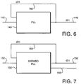
- a simple PLL 140 is shown in Figure 6 .
- the PLL has an input 140, and output 148, with a time delay dtl inherent between the output of the PLL and the load (not shown).
- a feedback signal 146 has the identical delay dtl. As a result, the output will be phase locked to the signal as seen at the load.
- Skewed drivers are defined as those with a single input, and two or more outputs, with each output having a different phase angle, or delay, relative to the input.
- a variation of the PLL is the skewed PLL, shown in Figure 7 .
- the skewed PLL has input 152, and two separate outputs 156 and 158.
- the skewed PLL has a phase delay between the outputs 156 and 158, which may be used to drive multiple clocks required by this invention.
- any PLL output can be used to generate the delayed clock or phase shifted clock.
- two methods are used to produce a phase shifted, or delayed, clock.
- the phase shift, or delay of the PLL may be created in a number of ways.
- the PLL may contain a delay internal to the PLL, so that the output will be automatically delayed relative to the input.
- a delay line or circuit may be inserted in series between two PLL circuits, creating a cascaded PLL delay circuit.
- One proposed method is to use the clock generated by the DIMM to drive the first bank of SDRAMs . If the clock delay is done on the DIMM, a printed wire length is incorporated to accurately give the required delay to generate a shifted clock. This shifted clock is then used to drive a second PLL. The output of the second PLL is the delayed clock used to drive the second of the two banks of SDRAMs.
- the wire length required is determined via simulation, theoretical, and trial and error methods.
- the DIMM uses a delayed clock also located on the motherboard, to drive the PLL, located on the DIMM.
- the outputs of the PLL will drive the SDRAM chips of the bank.
- phase delayed clock Other methods of creating a second phase delayed clock include use of delay line chips can also be used to accomplish the predetermined phase shift required for the delayed clock. Also, combination of passive and active circuits can be employed to accomplish the desired phase shift. These include programmable delay lines currently commercially available. These devices and techniques are well known in the art, and will not be described further herein.
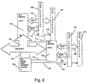
- the DIMM modules themselves become memory banks.
- the DIMMs inserted into DIMM connector 166 and 168 form the equivalent of a first and second memory bank, respectively.
- the data 172 to and from the first DIMM, in connector 166 is switched on and off the data bus by FET switch 160.
- the data 170 is switched to and from the second DIMM, mounted in DIMM connector 168, by the same FET switch 160.
- the Phase Locked Loop Phase shift doubler produces clock signals 174 and 176, which are in quadrature with respect to each other, to enable the first DIMM, and then the second DIMM.
- Enable signal 180 generated by the PLL circuit 164, generates signals analogous to FET EN A 112 and FET EN B 113 of Figure 3A , alternately enabling the first DIMM and the second DIMM in the current embodiment.
- Figure 8 also shows a second set of DIMM connectors 182, 184, in which a third and fourth memory bank is created by the insertion of two more DIMMs.
- These two additional DIMMs operated in exactly the same manner as the first and second DIMMs, having their own FET switch 178, quadrature clock signals 190 and 192, etc.
- each DDR DIMM serving the function of the DDR data bank in the previous embodiments.
- This embodiment has the advantage of using DIMMs in their currently available forms, thus requiring only the manufacture of a motherboard to enjoy the advantages in speed and access time of the current invention.
Landscapes
- Engineering & Computer Science (AREA)
- Theoretical Computer Science (AREA)
- Physics & Mathematics (AREA)
- General Engineering & Computer Science (AREA)
- General Physics & Mathematics (AREA)
- Dram (AREA)
Applications Claiming Priority (3)
| Application Number | Priority Date | Filing Date | Title |
|---|---|---|---|
| US09/572,641 US6446158B1 (en) | 1999-05-17 | 2000-05-17 | Memory system using FET switches to select memory banks |
| US572641 | 2000-05-17 | ||
| PCT/US2001/015592 WO2001088714A1 (en) | 2000-05-17 | 2001-05-15 | Multiple access per cycle in a multiple bank dimm |
Publications (3)
| Publication Number | Publication Date |
|---|---|
| EP1290561A1 EP1290561A1 (en) | 2003-03-12 |
| EP1290561A4 EP1290561A4 (en) | 2006-10-11 |
| EP1290561B1 true EP1290561B1 (en) | 2019-10-23 |
Family
ID=24288730
Family Applications (1)
| Application Number | Title | Priority Date | Filing Date |
|---|---|---|---|
| EP01937381.0A Expired - Lifetime EP1290561B1 (en) | 2000-05-17 | 2001-05-15 | Multiple access per cycle in a multiple bank dimm |
Country Status (6)
| Country | Link |
|---|---|
| US (1) | US6446158B1 (enExample) |
| EP (1) | EP1290561B1 (enExample) |
| JP (1) | JP4769953B2 (enExample) |
| CN (1) | CN1436331A (enExample) |
| AU (1) | AU2001263124A1 (enExample) |
| WO (1) | WO2001088714A1 (enExample) |
Families Citing this family (94)
| Publication number | Priority date | Publication date | Assignee | Title |
|---|---|---|---|---|
| US6323060B1 (en) | 1999-05-05 | 2001-11-27 | Dense-Pac Microsystems, Inc. | Stackable flex circuit IC package and method of making same |
| US6643752B1 (en) | 1999-12-09 | 2003-11-04 | Rambus Inc. | Transceiver with latency alignment circuitry |
| US7363422B2 (en) | 2000-01-05 | 2008-04-22 | Rambus Inc. | Configurable width buffered module |
| US20050010737A1 (en) * | 2000-01-05 | 2005-01-13 | Fred Ware | Configurable width buffered module having splitter elements |
| US6502161B1 (en) | 2000-01-05 | 2002-12-31 | Rambus Inc. | Memory system including a point-to-point linked memory subsystem |
| US7356639B2 (en) * | 2000-01-05 | 2008-04-08 | Rambus Inc. | Configurable width buffered module having a bypass circuit |
| US7017002B2 (en) * | 2000-01-05 | 2006-03-21 | Rambus, Inc. | System featuring a master device, a buffer device and a plurality of integrated circuit memory devices |
| US7404032B2 (en) | 2000-01-05 | 2008-07-22 | Rambus Inc. | Configurable width buffered module having switch elements |
| US7266634B2 (en) * | 2000-01-05 | 2007-09-04 | Rambus Inc. | Configurable width buffered module having flyby elements |
| US6262895B1 (en) | 2000-01-13 | 2001-07-17 | John A. Forthun | Stackable chip package with flex carrier |
| KR100587052B1 (ko) * | 2000-06-30 | 2006-06-07 | 주식회사 하이닉스반도체 | 고속 인터페이스용 장치 |
| US6839820B1 (en) * | 2000-07-20 | 2005-01-04 | Silicon Graphics, Inc. | Method and system for controlling data access between at least two memory arrangements |
| TW526417B (en) * | 2000-08-03 | 2003-04-01 | Asustek Comp Inc | Control circuit for providing applications of unbuffered dual in-line memory modules (DIMM) on system supporting only registered DIMM chipset |
| US6737891B2 (en) | 2001-02-01 | 2004-05-18 | Chris Karabatsos | Tri-directional, high-speed bus switch |
| DE10106817C1 (de) * | 2001-02-14 | 2002-08-08 | Infineon Technologies Ag | Speicheranordnung |
| US6629225B2 (en) * | 2001-05-31 | 2003-09-30 | Intel Corporation | Method and apparatus for control calibration of multiple memory modules within a memory channel |
| US7202555B2 (en) | 2001-10-26 | 2007-04-10 | Staktek Group L.P. | Pitch change and chip scale stacking system and method |
| US7371609B2 (en) | 2001-10-26 | 2008-05-13 | Staktek Group L.P. | Stacked module systems and methods |
| US6914324B2 (en) | 2001-10-26 | 2005-07-05 | Staktek Group L.P. | Memory expansion and chip scale stacking system and method |
| US7053478B2 (en) | 2001-10-26 | 2006-05-30 | Staktek Group L.P. | Pitch change and chip scale stacking system |
| US20030234443A1 (en) | 2001-10-26 | 2003-12-25 | Staktek Group, L.P. | Low profile stacking system and method |
| US20060255446A1 (en) | 2001-10-26 | 2006-11-16 | Staktek Group, L.P. | Stacked modules and method |
| US7310458B2 (en) | 2001-10-26 | 2007-12-18 | Staktek Group L.P. | Stacked module systems and methods |
| US7026708B2 (en) | 2001-10-26 | 2006-04-11 | Staktek Group L.P. | Low profile chip scale stacking system and method |
| US6940729B2 (en) | 2001-10-26 | 2005-09-06 | Staktek Group L.P. | Integrated circuit stacking system and method |
| US6956284B2 (en) * | 2001-10-26 | 2005-10-18 | Staktek Group L.P. | Integrated circuit stacking system and method |
| US7656678B2 (en) | 2001-10-26 | 2010-02-02 | Entorian Technologies, Lp | Stacked module systems |
| US7485951B2 (en) | 2001-10-26 | 2009-02-03 | Entorian Technologies, Lp | Modularized die stacking system and method |
| US7081373B2 (en) | 2001-12-14 | 2006-07-25 | Staktek Group, L.P. | CSP chip stack with flex circuit |
| US7003684B2 (en) * | 2002-03-27 | 2006-02-21 | Via Technologies, Inc. | Memory control chip, control method and control circuit |
| TW559809B (en) * | 2002-03-27 | 2003-11-01 | Via Tech Inc | Memory control chip, control method and control circuit |
| US20050050375A1 (en) * | 2003-08-29 | 2005-03-03 | Mark Novak | Memory interface system and method |
| US7542304B2 (en) | 2003-09-15 | 2009-06-02 | Entorian Technologies, Lp | Memory expansion and integrated circuit stacking system and method |
| US8250295B2 (en) * | 2004-01-05 | 2012-08-21 | Smart Modular Technologies, Inc. | Multi-rank memory module that emulates a memory module having a different number of ranks |
| WO2005083572A1 (ja) * | 2004-03-02 | 2005-09-09 | Sony Corporation | メモリ制御装置、メモリ制御方法、メモリ制御プログラムおよび画像撮像装置 |
| US7916574B1 (en) | 2004-03-05 | 2011-03-29 | Netlist, Inc. | Circuit providing load isolation and memory domain translation for memory module |
| US7289386B2 (en) | 2004-03-05 | 2007-10-30 | Netlist, Inc. | Memory module decoder |
| US7532537B2 (en) * | 2004-03-05 | 2009-05-12 | Netlist, Inc. | Memory module with a circuit providing load isolation and memory domain translation |
| US20060050492A1 (en) | 2004-09-03 | 2006-03-09 | Staktek Group, L.P. | Thin module system and method |
| US7616452B2 (en) | 2004-09-03 | 2009-11-10 | Entorian Technologies, Lp | Flex circuit constructions for high capacity circuit module systems and methods |
| US7443023B2 (en) | 2004-09-03 | 2008-10-28 | Entorian Technologies, Lp | High capacity thin module system |
| US7760513B2 (en) | 2004-09-03 | 2010-07-20 | Entorian Technologies Lp | Modified core for circuit module system and method |
| US7511968B2 (en) | 2004-09-03 | 2009-03-31 | Entorian Technologies, Lp | Buffered thin module system and method |
| US7468893B2 (en) | 2004-09-03 | 2008-12-23 | Entorian Technologies, Lp | Thin module system and method |
| US7324352B2 (en) | 2004-09-03 | 2008-01-29 | Staktek Group L.P. | High capacity thin module system and method |
| US7606049B2 (en) | 2004-09-03 | 2009-10-20 | Entorian Technologies, Lp | Module thermal management system and method |
| US7606050B2 (en) | 2004-09-03 | 2009-10-20 | Entorian Technologies, Lp | Compact module system and method |
| US7423885B2 (en) | 2004-09-03 | 2008-09-09 | Entorian Technologies, Lp | Die module system |
| US7542297B2 (en) | 2004-09-03 | 2009-06-02 | Entorian Technologies, Lp | Optimized mounting area circuit module system and method |
| US7446410B2 (en) | 2004-09-03 | 2008-11-04 | Entorian Technologies, Lp | Circuit module with thermal casing systems |
| US7522421B2 (en) | 2004-09-03 | 2009-04-21 | Entorian Technologies, Lp | Split core circuit module |
| US7606040B2 (en) | 2004-09-03 | 2009-10-20 | Entorian Technologies, Lp | Memory module system and method |
| US7579687B2 (en) | 2004-09-03 | 2009-08-25 | Entorian Technologies, Lp | Circuit module turbulence enhancement systems and methods |
| US7289327B2 (en) | 2006-02-27 | 2007-10-30 | Stakick Group L.P. | Active cooling methods and apparatus for modules |
| US7280428B2 (en) | 2004-09-30 | 2007-10-09 | Rambus Inc. | Multi-column addressing mode memory system including an integrated circuit memory device |
| US7571296B2 (en) * | 2004-11-11 | 2009-08-04 | Nvidia Corporation | Memory controller-adaptive 1T/2T timing control |
| US8595459B2 (en) | 2004-11-29 | 2013-11-26 | Rambus Inc. | Micro-threaded memory |
| US7309914B2 (en) | 2005-01-20 | 2007-12-18 | Staktek Group L.P. | Inverted CSP stacking system and method |
| US7033861B1 (en) | 2005-05-18 | 2006-04-25 | Staktek Group L.P. | Stacked module systems and method |
| US20060277355A1 (en) * | 2005-06-01 | 2006-12-07 | Mark Ellsberry | Capacity-expanding memory device |
| US7464225B2 (en) | 2005-09-26 | 2008-12-09 | Rambus Inc. | Memory module including a plurality of integrated circuit memory devices and a plurality of buffer devices in a matrix topology |
| US11328764B2 (en) | 2005-09-26 | 2022-05-10 | Rambus Inc. | Memory system topologies including a memory die stack |
| US7562271B2 (en) | 2005-09-26 | 2009-07-14 | Rambus Inc. | Memory system topologies including a buffer device and an integrated circuit memory device |
| US7576995B2 (en) | 2005-11-04 | 2009-08-18 | Entorian Technologies, Lp | Flex circuit apparatus and method for adding capacitance while conserving circuit board surface area |
| US7508069B2 (en) | 2006-01-11 | 2009-03-24 | Entorian Technologies, Lp | Managed memory component |
| US7508058B2 (en) | 2006-01-11 | 2009-03-24 | Entorian Technologies, Lp | Stacked integrated circuit module |
| US7608920B2 (en) | 2006-01-11 | 2009-10-27 | Entorian Technologies, Lp | Memory card and method for devising |
| US7304382B2 (en) | 2006-01-11 | 2007-12-04 | Staktek Group L.P. | Managed memory component |
| US7605454B2 (en) | 2006-01-11 | 2009-10-20 | Entorian Technologies, Lp | Memory card and method for devising |
| US7511969B2 (en) | 2006-02-02 | 2009-03-31 | Entorian Technologies, Lp | Composite core circuit module system and method |
| US20070260841A1 (en) | 2006-05-02 | 2007-11-08 | Hampel Craig E | Memory module with reduced access granularity |
| US7468553B2 (en) | 2006-10-20 | 2008-12-23 | Entorian Technologies, Lp | Stackable micropackages and stacked modules |
| US7417310B2 (en) | 2006-11-02 | 2008-08-26 | Entorian Technologies, Lp | Circuit module having force resistant construction |
| US7937537B2 (en) * | 2007-09-24 | 2011-05-03 | International Business Machines Corporation | Memory switching data processing system |
| US7945740B2 (en) * | 2007-09-24 | 2011-05-17 | International Business Machines Corporation | Structure for a memory switching data processing system |
| US8154901B1 (en) | 2008-04-14 | 2012-04-10 | Netlist, Inc. | Circuit providing load isolation and noise reduction |
| US8516185B2 (en) | 2009-07-16 | 2013-08-20 | Netlist, Inc. | System and method utilizing distributed byte-wise buffers on a memory module |
| US8417870B2 (en) | 2009-07-16 | 2013-04-09 | Netlist, Inc. | System and method of increasing addressable memory space on a memory board |
| US9128632B2 (en) | 2009-07-16 | 2015-09-08 | Netlist, Inc. | Memory module with distributed data buffers and method of operation |
| US8402208B2 (en) * | 2009-10-06 | 2013-03-19 | Dell Products L.P. | Configurable memory controller/memory module communication system |
| KR101796116B1 (ko) | 2010-10-20 | 2017-11-10 | 삼성전자 주식회사 | 반도체 장치, 이를 포함하는 메모리 모듈, 메모리 시스템 및 그 동작방법 |
| WO2012061633A2 (en) | 2010-11-03 | 2012-05-10 | Netlist, Inc. | Method and apparatus for optimizing driver load in a memory package |
| US9477597B2 (en) * | 2011-03-25 | 2016-10-25 | Nvidia Corporation | Techniques for different memory depths on different partitions |
| US8701057B2 (en) | 2011-04-11 | 2014-04-15 | Nvidia Corporation | Design, layout, and manufacturing techniques for multivariant integrated circuits |
| US9529712B2 (en) | 2011-07-26 | 2016-12-27 | Nvidia Corporation | Techniques for balancing accesses to memory having different memory types |
| US9268719B2 (en) | 2011-08-05 | 2016-02-23 | Rambus Inc. | Memory signal buffers and modules supporting variable access granularity |
| JP2013061767A (ja) * | 2011-09-13 | 2013-04-04 | Elpida Memory Inc | メモリシステムおよびメモリモジュール |
| CN110428855B (zh) | 2013-07-27 | 2023-09-22 | 奈特力斯股份有限公司 | 具有本地分别同步的内存模块 |
| KR101707266B1 (ko) * | 2013-08-29 | 2017-02-15 | 엘에스산전 주식회사 | Plc에서의 os의 업데이트 장치 및 방법 |
| KR102509330B1 (ko) * | 2018-04-16 | 2023-03-14 | 에스케이하이닉스 주식회사 | 샘플링 회로 및 이를 이용한 반도체 메모리 장치 |
| US10963404B2 (en) | 2018-06-25 | 2021-03-30 | Intel Corporation | High bandwidth DIMM |
| US10884958B2 (en) | 2018-06-25 | 2021-01-05 | Intel Corporation | DIMM for a high bandwidth memory channel |
| US10635357B2 (en) | 2018-07-03 | 2020-04-28 | Nvidia Corporation | Method for overlapping memory accesses |
| US11699471B2 (en) | 2019-09-25 | 2023-07-11 | Intel Corporation | Synchronous dynamic random access memory (SDRAM) dual in-line memory module (DIMM) having increased per data pin bandwidth |
Citations (1)
| Publication number | Priority date | Publication date | Assignee | Title |
|---|---|---|---|---|
| US5691955A (en) * | 1995-09-05 | 1997-11-25 | Mitsubishi Denki Kabushiki Kaisha | Synchronous semiconductor memory device operating in synchronization with external clock signal |
Family Cites Families (10)
| Publication number | Priority date | Publication date | Assignee | Title |
|---|---|---|---|---|
| JPH03113547A (ja) * | 1989-09-28 | 1991-05-14 | Casio Comput Co Ltd | 記憶制御装置 |
| JPH03269662A (ja) * | 1990-03-20 | 1991-12-02 | Fujitsu Ltd | 高速メモリアクセス方式 |
| US5261068A (en) * | 1990-05-25 | 1993-11-09 | Dell Usa L.P. | Dual path memory retrieval system for an interleaved dynamic RAM memory unit |
| JPH06202933A (ja) * | 1992-12-28 | 1994-07-22 | Toshiba Corp | 同期式大規模集積回路記憶装置 |
| JPH07282000A (ja) * | 1994-04-04 | 1995-10-27 | Hitachi Ltd | バスインタフェース回路及びデータ転送システム |
| US5666322A (en) * | 1995-09-21 | 1997-09-09 | Nec Electronics, Inc. | Phase-locked loop timing controller in an integrated circuit memory |
| US5950223A (en) * | 1997-06-19 | 1999-09-07 | Silicon Magic Corporation | Dual-edge extended data out memory |
| US6233650B1 (en) * | 1998-04-01 | 2001-05-15 | Intel Corporation | Using FET switches for large memory arrays |
| JP4540137B2 (ja) * | 1998-07-24 | 2010-09-08 | ルネサスエレクトロニクス株式会社 | 同期型半導体記憶装置 |
| DE19849909A1 (de) * | 1998-10-29 | 2000-05-04 | Philips Corp Intellectual Pty | Schaltungsanordnung zum Verarbeiten binärer Signale |
-
2000
- 2000-05-17 US US09/572,641 patent/US6446158B1/en not_active Expired - Lifetime
-
2001
- 2001-05-15 CN CN01809630A patent/CN1436331A/zh active Pending
- 2001-05-15 JP JP2001585044A patent/JP4769953B2/ja not_active Expired - Fee Related
- 2001-05-15 EP EP01937381.0A patent/EP1290561B1/en not_active Expired - Lifetime
- 2001-05-15 AU AU2001263124A patent/AU2001263124A1/en not_active Abandoned
- 2001-05-15 WO PCT/US2001/015592 patent/WO2001088714A1/en not_active Ceased
Patent Citations (1)
| Publication number | Priority date | Publication date | Assignee | Title |
|---|---|---|---|---|
| US5691955A (en) * | 1995-09-05 | 1997-11-25 | Mitsubishi Denki Kabushiki Kaisha | Synchronous semiconductor memory device operating in synchronization with external clock signal |
Also Published As
| Publication number | Publication date |
|---|---|
| WO2001088714A1 (en) | 2001-11-22 |
| EP1290561A1 (en) | 2003-03-12 |
| CN1436331A (zh) | 2003-08-13 |
| AU2001263124A1 (en) | 2001-11-26 |
| US6446158B1 (en) | 2002-09-03 |
| JP2004511026A (ja) | 2004-04-08 |
| JP4769953B2 (ja) | 2011-09-07 |
| EP1290561A4 (en) | 2006-10-11 |
Similar Documents
| Publication | Publication Date | Title |
|---|---|---|
| EP1290561B1 (en) | Multiple access per cycle in a multiple bank dimm | |
| US8458507B2 (en) | Bus frequency adjustment circuitry for use in a dynamic random access memory device | |
| US7612621B2 (en) | System for providing open-loop quadrature clock generation | |
| JP4159415B2 (ja) | メモリモジュール及びメモリシステム | |
| US8422263B2 (en) | Load reduced memory module and memory system including the same | |
| US8966208B2 (en) | Semiconductor memory device with plural memory die and controller die | |
| EP2319044B1 (en) | Memory system and method using stacked memory device dice, and system using the memory system | |
| KR100382736B1 (ko) | 독출동작과 기입동작시 서로 다른 데이터율을 갖는 반도체메모리장치 및 이를 채용하는 시스템 | |
| JP3929116B2 (ja) | メモリサブシステム | |
| KR100601149B1 (ko) | 데이터 전송장치 | |
| US7872937B2 (en) | Data driver circuit for a dynamic random access memory (DRAM) controller or the like and method therefor | |
| KR100626375B1 (ko) | 고주파로 동작하는 반도체 메모리 장치 및 모듈 | |
| US20100312956A1 (en) | Load reduced memory module | |
| US11146275B2 (en) | Signal generation circuit and a semiconductor apparatus using the signal generation circuit | |
| US8053911B2 (en) | Semiconductor device and data processor | |
| US20100312925A1 (en) | Load reduced memory module | |
| JP2003337742A (ja) | メモリシステムとモジュール及びレジスタ | |
| JPH1166852A (ja) | 半導体記憶装置 | |
| Wang et al. | A 500-Mb/s quadruple data rate SDRAM interface using a skew cancellation technique | |
| CN118899020B (zh) | 片上终结信号产生电路以及存储系统 | |
| JP2008123543A (ja) | データ伝送方法、システム及びデバイス | |
| US20020181290A1 (en) | Data output interface, in particular for semiconductor memories |
Legal Events
| Date | Code | Title | Description |
|---|---|---|---|
| PUAI | Public reference made under article 153(3) epc to a published international application that has entered the european phase |
Free format text: ORIGINAL CODE: 0009012 |
|
| 17P | Request for examination filed |
Effective date: 20021115 |
|
| AK | Designated contracting states |
Designated state(s): AT BE CH CY DE DK ES FI FR GB GR IE IT LI LU MC NL PT SE TR Kind code of ref document: A1 Designated state(s): AT BE CH CY DE DK ES FI FR GB GR IE IT LI LU MC NL PT SE TR |
|
| AX | Request for extension of the european patent |
Extension state: AL LT LV MK RO SI |
|
| A4 | Supplementary search report drawn up and despatched |
Effective date: 20060911 |
|
| 17Q | First examination report despatched |
Effective date: 20080402 |
|
| RAP1 | Party data changed (applicant data changed or rights of an application transferred) |
Owner name: URENSCHI ASSETS LIMITED LIABILITY COMPANY |
|
| RIN1 | Information on inventor provided before grant (corrected) |
Inventor name: KARABATSOS, CHRIS |
|
| RAP1 | Party data changed (applicant data changed or rights of an application transferred) |
Owner name: CALLAHAN CELLULAR L.L.C. |
|
| GRAP | Despatch of communication of intention to grant a patent |
Free format text: ORIGINAL CODE: EPIDOSNIGR1 |
|
| STAA | Information on the status of an ep patent application or granted ep patent |
Free format text: STATUS: GRANT OF PATENT IS INTENDED |
|
| INTG | Intention to grant announced |
Effective date: 20181130 |
|
| GRAJ | Information related to disapproval of communication of intention to grant by the applicant or resumption of examination proceedings by the epo deleted |
Free format text: ORIGINAL CODE: EPIDOSDIGR1 |
|
| STAA | Information on the status of an ep patent application or granted ep patent |
Free format text: STATUS: EXAMINATION IS IN PROGRESS |
|
| INTC | Intention to grant announced (deleted) | ||
| GRAP | Despatch of communication of intention to grant a patent |
Free format text: ORIGINAL CODE: EPIDOSNIGR1 |
|
| STAA | Information on the status of an ep patent application or granted ep patent |
Free format text: STATUS: GRANT OF PATENT IS INTENDED |
|
| INTG | Intention to grant announced |
Effective date: 20190510 |
|
| GRAS | Grant fee paid |
Free format text: ORIGINAL CODE: EPIDOSNIGR3 |
|
| GRAA | (expected) grant |
Free format text: ORIGINAL CODE: 0009210 |
|
| STAA | Information on the status of an ep patent application or granted ep patent |
Free format text: STATUS: THE PATENT HAS BEEN GRANTED |
|
| AK | Designated contracting states |
Kind code of ref document: B1 Designated state(s): AT BE CH CY DE DK ES FI FR GB GR IE IT LI LU MC NL PT SE TR |
|
| REG | Reference to a national code |
Ref country code: GB Ref legal event code: FG4D |
|
| REG | Reference to a national code |
Ref country code: CH Ref legal event code: EP |
|
| REG | Reference to a national code |
Ref country code: IE Ref legal event code: FG4D |
|
| REG | Reference to a national code |
Ref country code: DE Ref legal event code: R096 Ref document number: 60151201 Country of ref document: DE |
|
| REG | Reference to a national code |
Ref country code: AT Ref legal event code: REF Ref document number: 1194442 Country of ref document: AT Kind code of ref document: T Effective date: 20191115 |
|
| REG | Reference to a national code |
Ref country code: NL Ref legal event code: MP Effective date: 20191023 |
|
| PG25 | Lapsed in a contracting state [announced via postgrant information from national office to epo] |
Ref country code: GR Free format text: LAPSE BECAUSE OF FAILURE TO SUBMIT A TRANSLATION OF THE DESCRIPTION OR TO PAY THE FEE WITHIN THE PRESCRIBED TIME-LIMIT Effective date: 20200124 Ref country code: NL Free format text: LAPSE BECAUSE OF FAILURE TO SUBMIT A TRANSLATION OF THE DESCRIPTION OR TO PAY THE FEE WITHIN THE PRESCRIBED TIME-LIMIT Effective date: 20191023 Ref country code: FI Free format text: LAPSE BECAUSE OF FAILURE TO SUBMIT A TRANSLATION OF THE DESCRIPTION OR TO PAY THE FEE WITHIN THE PRESCRIBED TIME-LIMIT Effective date: 20191023 Ref country code: PT Free format text: LAPSE BECAUSE OF FAILURE TO SUBMIT A TRANSLATION OF THE DESCRIPTION OR TO PAY THE FEE WITHIN THE PRESCRIBED TIME-LIMIT Effective date: 20200224 Ref country code: ES Free format text: LAPSE BECAUSE OF FAILURE TO SUBMIT A TRANSLATION OF THE DESCRIPTION OR TO PAY THE FEE WITHIN THE PRESCRIBED TIME-LIMIT Effective date: 20191023 Ref country code: SE Free format text: LAPSE BECAUSE OF FAILURE TO SUBMIT A TRANSLATION OF THE DESCRIPTION OR TO PAY THE FEE WITHIN THE PRESCRIBED TIME-LIMIT Effective date: 20191023 |
|
| REG | Reference to a national code |
Ref country code: DE Ref legal event code: R097 Ref document number: 60151201 Country of ref document: DE |
|
| PG25 | Lapsed in a contracting state [announced via postgrant information from national office to epo] |
Ref country code: DK Free format text: LAPSE BECAUSE OF FAILURE TO SUBMIT A TRANSLATION OF THE DESCRIPTION OR TO PAY THE FEE WITHIN THE PRESCRIBED TIME-LIMIT Effective date: 20191023 |
|
| REG | Reference to a national code |
Ref country code: AT Ref legal event code: MK05 Ref document number: 1194442 Country of ref document: AT Kind code of ref document: T Effective date: 20191023 |
|
| PLBE | No opposition filed within time limit |
Free format text: ORIGINAL CODE: 0009261 |
|
| STAA | Information on the status of an ep patent application or granted ep patent |
Free format text: STATUS: NO OPPOSITION FILED WITHIN TIME LIMIT |
|
| PG25 | Lapsed in a contracting state [announced via postgrant information from national office to epo] |
Ref country code: IT Free format text: LAPSE BECAUSE OF FAILURE TO SUBMIT A TRANSLATION OF THE DESCRIPTION OR TO PAY THE FEE WITHIN THE PRESCRIBED TIME-LIMIT Effective date: 20191023 |
|
| 26N | No opposition filed |
Effective date: 20200724 |
|
| PG25 | Lapsed in a contracting state [announced via postgrant information from national office to epo] |
Ref country code: AT Free format text: LAPSE BECAUSE OF FAILURE TO SUBMIT A TRANSLATION OF THE DESCRIPTION OR TO PAY THE FEE WITHIN THE PRESCRIBED TIME-LIMIT Effective date: 20191023 |
|
| REG | Reference to a national code |
Ref country code: DE Ref legal event code: R119 Ref document number: 60151201 Country of ref document: DE |
|
| PG25 | Lapsed in a contracting state [announced via postgrant information from national office to epo] |
Ref country code: CH Free format text: LAPSE BECAUSE OF NON-PAYMENT OF DUE FEES Effective date: 20200531 Ref country code: LI Free format text: LAPSE BECAUSE OF NON-PAYMENT OF DUE FEES Effective date: 20200531 Ref country code: MC Free format text: LAPSE BECAUSE OF FAILURE TO SUBMIT A TRANSLATION OF THE DESCRIPTION OR TO PAY THE FEE WITHIN THE PRESCRIBED TIME-LIMIT Effective date: 20191023 |
|
| REG | Reference to a national code |
Ref country code: BE Ref legal event code: MM Effective date: 20200531 |
|
| GBPC | Gb: european patent ceased through non-payment of renewal fee |
Effective date: 20200515 |
|
| PG25 | Lapsed in a contracting state [announced via postgrant information from national office to epo] |
Ref country code: LU Free format text: LAPSE BECAUSE OF NON-PAYMENT OF DUE FEES Effective date: 20200515 |
|
| PG25 | Lapsed in a contracting state [announced via postgrant information from national office to epo] |
Ref country code: GB Free format text: LAPSE BECAUSE OF NON-PAYMENT OF DUE FEES Effective date: 20200515 Ref country code: FR Free format text: LAPSE BECAUSE OF NON-PAYMENT OF DUE FEES Effective date: 20200531 Ref country code: IE Free format text: LAPSE BECAUSE OF NON-PAYMENT OF DUE FEES Effective date: 20200515 |
|
| PG25 | Lapsed in a contracting state [announced via postgrant information from national office to epo] |
Ref country code: DE Free format text: LAPSE BECAUSE OF NON-PAYMENT OF DUE FEES Effective date: 20201201 Ref country code: BE Free format text: LAPSE BECAUSE OF NON-PAYMENT OF DUE FEES Effective date: 20200531 |
|
| PG25 | Lapsed in a contracting state [announced via postgrant information from national office to epo] |
Ref country code: TR Free format text: LAPSE BECAUSE OF FAILURE TO SUBMIT A TRANSLATION OF THE DESCRIPTION OR TO PAY THE FEE WITHIN THE PRESCRIBED TIME-LIMIT Effective date: 20191023 Ref country code: CY Free format text: LAPSE BECAUSE OF FAILURE TO SUBMIT A TRANSLATION OF THE DESCRIPTION OR TO PAY THE FEE WITHIN THE PRESCRIBED TIME-LIMIT Effective date: 20191023 |