EP1264210B1 - Electrophoretic display - Google Patents
Electrophoretic display Download PDFInfo
- Publication number
- EP1264210B1 EP1264210B1 EP01914676A EP01914676A EP1264210B1 EP 1264210 B1 EP1264210 B1 EP 1264210B1 EP 01914676 A EP01914676 A EP 01914676A EP 01914676 A EP01914676 A EP 01914676A EP 1264210 B1 EP1264210 B1 EP 1264210B1
- Authority
- EP
- European Patent Office
- Prior art keywords
- electrophoretic
- microcups
- composition
- sealing
- electrophoretic display
- Prior art date
- Legal status (The legal status is an assumption and is not a legal conclusion. Google has not performed a legal analysis and makes no representation as to the accuracy of the status listed.)
- Expired - Lifetime
Links
- 238000000034 method Methods 0.000 claims abstract description 76
- 239000002904 solvent Substances 0.000 claims abstract description 73
- 230000008569 process Effects 0.000 claims abstract description 64
- 239000002245 particle Substances 0.000 claims abstract description 54
- 239000000049 pigment Substances 0.000 claims abstract description 54
- 239000000203 mixture Substances 0.000 claims description 72
- 238000007789 sealing Methods 0.000 claims description 54
- 239000010410 layer Substances 0.000 claims description 51
- 239000002243 precursor Substances 0.000 claims description 49
- 229920001187 thermosetting polymer Polymers 0.000 claims description 43
- 230000005855 radiation Effects 0.000 claims description 36
- 239000004020 conductor Substances 0.000 claims description 30
- 229920001169 thermoplastic Polymers 0.000 claims description 25
- 239000004416 thermosoftening plastic Substances 0.000 claims description 25
- 238000002360 preparation method Methods 0.000 claims description 21
- 229920002120 photoresistant polymer Polymers 0.000 claims description 19
- 239000006185 dispersion Substances 0.000 claims description 17
- 239000012790 adhesive layer Substances 0.000 claims description 12
- 229920000642 polymer Polymers 0.000 claims description 12
- 239000000463 material Substances 0.000 claims description 11
- 239000011877 solvent mixture Substances 0.000 claims description 11
- 238000000576 coating method Methods 0.000 claims description 10
- 230000005484 gravity Effects 0.000 claims description 10
- NIXOWILDQLNWCW-UHFFFAOYSA-M Acrylate Chemical compound [O-]C(=O)C=C NIXOWILDQLNWCW-UHFFFAOYSA-M 0.000 claims description 9
- GWEVSGVZZGPLCZ-UHFFFAOYSA-N Titan oxide Chemical compound O=[Ti]=O GWEVSGVZZGPLCZ-UHFFFAOYSA-N 0.000 claims description 9
- 239000011248 coating agent Substances 0.000 claims description 9
- 239000003086 colorant Substances 0.000 claims description 8
- 238000005192 partition Methods 0.000 claims description 8
- 238000004049 embossing Methods 0.000 claims description 7
- 238000011049 filling Methods 0.000 claims description 7
- 239000000654 additive Substances 0.000 claims description 6
- 230000009477 glass transition Effects 0.000 claims description 6
- 238000010030 laminating Methods 0.000 claims description 6
- 239000006228 supernatant Substances 0.000 claims description 6
- CERQOIWHTDAKMF-UHFFFAOYSA-M Methacrylate Chemical compound CC(=C)C([O-])=O CERQOIWHTDAKMF-UHFFFAOYSA-M 0.000 claims description 5
- 239000012463 white pigment Substances 0.000 claims description 5
- 229920001651 Cyanoacrylate Polymers 0.000 claims description 4
- 230000000996 additive effect Effects 0.000 claims description 4
- 238000001816 cooling Methods 0.000 claims description 4
- 238000010406 interfacial reaction Methods 0.000 claims description 4
- 238000004132 cross linking Methods 0.000 claims description 3
- 239000003960 organic solvent Substances 0.000 claims description 3
- 238000010894 electron beam technology Methods 0.000 claims description 2
- 238000003475 lamination Methods 0.000 claims description 2
- 125000003903 2-propenyl group Chemical group [H]C([*])([H])C([H])=C([H])[H] 0.000 claims 4
- 150000002118 epoxides Chemical class 0.000 claims 4
- 125000000524 functional group Chemical group 0.000 claims 4
- 125000000391 vinyl group Chemical group [H]C([*])=C([H])[H] 0.000 claims 4
- 229920002554 vinyl polymer Polymers 0.000 claims 4
- NLCKLZIHJQEMCU-UHFFFAOYSA-N cyano prop-2-enoate Chemical class C=CC(=O)OC#N NLCKLZIHJQEMCU-UHFFFAOYSA-N 0.000 claims 2
- 239000012948 isocyanate Substances 0.000 claims 2
- 150000002513 isocyanates Chemical class 0.000 claims 2
- 238000001704 evaporation Methods 0.000 claims 1
- 230000008020 evaporation Effects 0.000 claims 1
- 239000004014 plasticizer Substances 0.000 claims 1
- 238000004519 manufacturing process Methods 0.000 abstract description 12
- 239000010408 film Substances 0.000 description 30
- 239000012530 fluid Substances 0.000 description 27
- 239000000725 suspension Substances 0.000 description 16
- 239000003094 microcapsule Substances 0.000 description 15
- 239000000975 dye Substances 0.000 description 11
- 239000000853 adhesive Substances 0.000 description 9
- 230000001070 adhesive effect Effects 0.000 description 9
- 238000001723 curing Methods 0.000 description 9
- CSCPPACGZOOCGX-UHFFFAOYSA-N Acetone Chemical compound CC(C)=O CSCPPACGZOOCGX-UHFFFAOYSA-N 0.000 description 8
- -1 perfluoro Chemical group 0.000 description 8
- 239000000126 substance Substances 0.000 description 8
- 239000000178 monomer Substances 0.000 description 7
- 239000000243 solution Substances 0.000 description 7
- PXHVJJICTQNCMI-UHFFFAOYSA-N Nickel Chemical compound [Ni] PXHVJJICTQNCMI-UHFFFAOYSA-N 0.000 description 6
- YXFVVABEGXRONW-UHFFFAOYSA-N Toluene Chemical compound CC1=CC=CC=C1 YXFVVABEGXRONW-UHFFFAOYSA-N 0.000 description 6
- 239000003921 oil Substances 0.000 description 6
- 238000012695 Interfacial polymerization Methods 0.000 description 5
- 229920001577 copolymer Polymers 0.000 description 5
- 239000000047 product Substances 0.000 description 5
- 229920002799 BoPET Polymers 0.000 description 4
- KFZMGEQAYNKOFK-UHFFFAOYSA-N Isopropanol Chemical compound CC(C)O KFZMGEQAYNKOFK-UHFFFAOYSA-N 0.000 description 4
- 239000005041 Mylar™ Substances 0.000 description 4
- 239000003795 chemical substances by application Substances 0.000 description 4
- NNBZCPXTIHJBJL-UHFFFAOYSA-N decalin Chemical compound C1CCCC2CCCCC21 NNBZCPXTIHJBJL-UHFFFAOYSA-N 0.000 description 4
- 229910052751 metal Inorganic materials 0.000 description 4
- 239000002184 metal Substances 0.000 description 4
- 230000003287 optical effect Effects 0.000 description 4
- 239000004033 plastic Substances 0.000 description 4
- 229920003023 plastic Polymers 0.000 description 4
- 238000000935 solvent evaporation Methods 0.000 description 4
- 239000000758 substrate Substances 0.000 description 4
- OGIDPMRJRNCKJF-UHFFFAOYSA-N titanium oxide Inorganic materials [Ti]=O OGIDPMRJRNCKJF-UHFFFAOYSA-N 0.000 description 4
- XILPLWOGHPSJBK-UHFFFAOYSA-N 1,2-dichloro-4-(trifluoromethyl)benzene Chemical compound FC(F)(F)C1=CC=C(Cl)C(Cl)=C1 XILPLWOGHPSJBK-UHFFFAOYSA-N 0.000 description 3
- ZWEHNKRNPOVVGH-UHFFFAOYSA-N 2-Butanone Chemical compound CCC(C)=O ZWEHNKRNPOVVGH-UHFFFAOYSA-N 0.000 description 3
- RTZKZFJDLAIYFH-UHFFFAOYSA-N Diethyl ether Chemical compound CCOCC RTZKZFJDLAIYFH-UHFFFAOYSA-N 0.000 description 3
- OKKJLVBELUTLKV-UHFFFAOYSA-N Methanol Chemical compound OC OKKJLVBELUTLKV-UHFFFAOYSA-N 0.000 description 3
- 230000015572 biosynthetic process Effects 0.000 description 3
- 238000005323 electroforming Methods 0.000 description 3
- UHESRSKEBRADOO-UHFFFAOYSA-N ethyl carbamate;prop-2-enoic acid Chemical compound OC(=O)C=C.CCOC(N)=O UHESRSKEBRADOO-UHFFFAOYSA-N 0.000 description 3
- 238000002474 experimental method Methods 0.000 description 3
- 150000008282 halocarbons Chemical class 0.000 description 3
- 239000007791 liquid phase Substances 0.000 description 3
- 230000007246 mechanism Effects 0.000 description 3
- 229910052759 nickel Inorganic materials 0.000 description 3
- 230000000630 rising effect Effects 0.000 description 3
- 238000004062 sedimentation Methods 0.000 description 3
- 125000006850 spacer group Chemical group 0.000 description 3
- 239000004094 surface-active agent Substances 0.000 description 3
- OVISMSJCKCDOPU-UHFFFAOYSA-N 1,6-dichlorohexane Chemical compound ClCCCCCCCl OVISMSJCKCDOPU-UHFFFAOYSA-N 0.000 description 2
- FIHBHSQYSYVZQE-UHFFFAOYSA-N 6-prop-2-enoyloxyhexyl prop-2-enoate Chemical compound C=CC(=O)OCCCCCCOC(=O)C=C FIHBHSQYSYVZQE-UHFFFAOYSA-N 0.000 description 2
- VYZAMTAEIAYCRO-UHFFFAOYSA-N Chromium Chemical compound [Cr] VYZAMTAEIAYCRO-UHFFFAOYSA-N 0.000 description 2
- 239000004831 Hot glue Substances 0.000 description 2
- MWCLLHOVUTZFKS-UHFFFAOYSA-N Methyl cyanoacrylate Chemical compound COC(=O)C(=C)C#N MWCLLHOVUTZFKS-UHFFFAOYSA-N 0.000 description 2
- CTQNGGLPUBDAKN-UHFFFAOYSA-N O-Xylene Chemical compound CC1=CC=CC=C1C CTQNGGLPUBDAKN-UHFFFAOYSA-N 0.000 description 2
- 239000004820 Pressure-sensitive adhesive Substances 0.000 description 2
- 238000003848 UV Light-Curing Methods 0.000 description 2
- 239000006229 carbon black Substances 0.000 description 2
- 238000005354 coacervation Methods 0.000 description 2
- 238000009713 electroplating Methods 0.000 description 2
- 239000011521 glass Substances 0.000 description 2
- 238000011065 in-situ storage Methods 0.000 description 2
- 239000004615 ingredient Substances 0.000 description 2
- 239000007788 liquid Substances 0.000 description 2
- 239000011159 matrix material Substances 0.000 description 2
- 150000002924 oxiranes Chemical class 0.000 description 2
- 239000012071 phase Substances 0.000 description 2
- 229920002493 poly(chlorotrifluoroethylene) Polymers 0.000 description 2
- 229920003229 poly(methyl methacrylate) Polymers 0.000 description 2
- 238000006116 polymerization reaction Methods 0.000 description 2
- 239000004926 polymethyl methacrylate Substances 0.000 description 2
- 239000000843 powder Substances 0.000 description 2
- KCTAWXVAICEBSD-UHFFFAOYSA-N prop-2-enoyloxy prop-2-eneperoxoate Chemical compound C=CC(=O)OOOC(=O)C=C KCTAWXVAICEBSD-UHFFFAOYSA-N 0.000 description 2
- 230000004044 response Effects 0.000 description 2
- 230000035945 sensitivity Effects 0.000 description 2
- APSBXTVYXVQYAB-UHFFFAOYSA-M sodium docusate Chemical compound [Na+].CCCCC(CC)COC(=O)CC(S([O-])(=O)=O)C(=O)OCC(CC)CCCC APSBXTVYXVQYAB-UHFFFAOYSA-M 0.000 description 2
- KZNICNPSHKQLFF-UHFFFAOYSA-N succinimide Chemical compound O=C1CCC(=O)N1 KZNICNPSHKQLFF-UHFFFAOYSA-N 0.000 description 2
- YCUVUDODLRLVIC-VPHDGDOJSA-N sudan black b Chemical compound C1=CC(=C23)NC(C)(C)NC2=CC=CC3=C1\N=N\C(C1=CC=CC=C11)=CC=C1\N=N\C1=CC=CC=C1 YCUVUDODLRLVIC-VPHDGDOJSA-N 0.000 description 2
- 239000008096 xylene Substances 0.000 description 2
- OJOWICOBYCXEKR-APPZFPTMSA-N (1S,4R)-5-ethylidenebicyclo[2.2.1]hept-2-ene Chemical compound CC=C1C[C@@H]2C[C@@H]1C=C2 OJOWICOBYCXEKR-APPZFPTMSA-N 0.000 description 1
- FBTKIMWGAQACHU-UHFFFAOYSA-N 1,1-dichlorononane Chemical compound CCCCCCCCC(Cl)Cl FBTKIMWGAQACHU-UHFFFAOYSA-N 0.000 description 1
- USPWUOFNOTUBAD-UHFFFAOYSA-N 1,2,3,4,5-pentafluoro-6-(trifluoromethyl)benzene Chemical compound FC1=C(F)C(F)=C(C(F)(F)F)C(F)=C1F USPWUOFNOTUBAD-UHFFFAOYSA-N 0.000 description 1
- UWTFGHPTJQPZQP-UHFFFAOYSA-N 1,2,3,4-tetrafluoro-5,6-bis(trifluoromethyl)benzene Chemical group FC1=C(F)C(F)=C(C(F)(F)F)C(C(F)(F)F)=C1F UWTFGHPTJQPZQP-UHFFFAOYSA-N 0.000 description 1
- FBKFIAIRSQOXJR-UHFFFAOYSA-N 1,2,3-trichloro-5-(trifluoromethyl)benzene Chemical compound FC(F)(F)C1=CC(Cl)=C(Cl)C(Cl)=C1 FBKFIAIRSQOXJR-UHFFFAOYSA-N 0.000 description 1
- BJYHBJUWZMHGGQ-UHFFFAOYSA-N 1,2-dichloro-3-(trifluoromethyl)benzene Chemical compound FC(F)(F)C1=CC=CC(Cl)=C1Cl BJYHBJUWZMHGGQ-UHFFFAOYSA-N 0.000 description 1
- GNPWYHFXSMINJQ-UHFFFAOYSA-N 1,2-dimethyl-3-(1-phenylethyl)benzene Chemical compound C=1C=CC(C)=C(C)C=1C(C)C1=CC=CC=C1 GNPWYHFXSMINJQ-UHFFFAOYSA-N 0.000 description 1
- OCQDPIXQTSYZJL-UHFFFAOYSA-N 1,4-bis(butylamino)anthracene-9,10-dione Chemical compound O=C1C2=CC=CC=C2C(=O)C2=C1C(NCCCC)=CC=C2NCCCC OCQDPIXQTSYZJL-UHFFFAOYSA-N 0.000 description 1
- 239000005968 1-Decanol Substances 0.000 description 1
- KGCDGLXSBHJAHZ-UHFFFAOYSA-N 1-chloro-2,3,4,5,6-pentafluorobenzene Chemical compound FC1=C(F)C(F)=C(Cl)C(F)=C1F KGCDGLXSBHJAHZ-UHFFFAOYSA-N 0.000 description 1
- MFYSUUPKMDJYPF-UHFFFAOYSA-N 2-[(4-methyl-2-nitrophenyl)diazenyl]-3-oxo-n-phenylbutanamide Chemical compound C=1C=CC=CC=1NC(=O)C(C(=O)C)N=NC1=CC=C(C)C=C1[N+]([O-])=O MFYSUUPKMDJYPF-UHFFFAOYSA-N 0.000 description 1
- IAFBRPFISOTXSO-UHFFFAOYSA-N 2-[[2-chloro-4-[3-chloro-4-[[1-(2,4-dimethylanilino)-1,3-dioxobutan-2-yl]diazenyl]phenyl]phenyl]diazenyl]-n-(2,4-dimethylphenyl)-3-oxobutanamide Chemical compound C=1C=C(C)C=C(C)C=1NC(=O)C(C(=O)C)N=NC(C(=C1)Cl)=CC=C1C(C=C1Cl)=CC=C1N=NC(C(C)=O)C(=O)NC1=CC=C(C)C=C1C IAFBRPFISOTXSO-UHFFFAOYSA-N 0.000 description 1
- LQZFGPJGXVFSTR-UHFFFAOYSA-N 2-[[2-chloro-4-[3-chloro-4-[[1-(2-methylanilino)-1,3-dioxobutan-2-yl]diazenyl]phenyl]phenyl]diazenyl]-n-(2-methylphenyl)-3-oxobutanamide Chemical compound C=1C=CC=C(C)C=1NC(=O)C(C(=O)C)N=NC(C(=C1)Cl)=CC=C1C(C=C1Cl)=CC=C1N=NC(C(C)=O)C(=O)NC1=CC=CC=C1C LQZFGPJGXVFSTR-UHFFFAOYSA-N 0.000 description 1
- RIWRBSMFKVOJMN-UHFFFAOYSA-N 2-methyl-1-phenylpropan-2-ol Chemical compound CC(C)(O)CC1=CC=CC=C1 RIWRBSMFKVOJMN-UHFFFAOYSA-N 0.000 description 1
- NIXOWILDQLNWCW-UHFFFAOYSA-N Acrylic acid Chemical compound OC(=O)C=C NIXOWILDQLNWCW-UHFFFAOYSA-N 0.000 description 1
- 229920002126 Acrylic acid copolymer Polymers 0.000 description 1
- OKTJSMMVPCPJKN-UHFFFAOYSA-N Carbon Chemical compound [C] OKTJSMMVPCPJKN-UHFFFAOYSA-N 0.000 description 1
- XZMCDFZZKTWFGF-UHFFFAOYSA-N Cyanamide Chemical compound NC#N XZMCDFZZKTWFGF-UHFFFAOYSA-N 0.000 description 1
- CERQOIWHTDAKMF-UHFFFAOYSA-N Methacrylic acid Chemical compound CC(=C)C(O)=O CERQOIWHTDAKMF-UHFFFAOYSA-N 0.000 description 1
- 239000005662 Paraffin oil Substances 0.000 description 1
- 239000004793 Polystyrene Substances 0.000 description 1
- NRCMAYZCPIVABH-UHFFFAOYSA-N Quinacridone Chemical compound N1C2=CC=CC=C2C(=O)C2=C1C=C1C(=O)C3=CC=CC=C3NC1=C2 NRCMAYZCPIVABH-UHFFFAOYSA-N 0.000 description 1
- 229920002472 Starch Polymers 0.000 description 1
- QYKIQEUNHZKYBP-UHFFFAOYSA-N Vinyl ether Chemical compound C=COC=C QYKIQEUNHZKYBP-UHFFFAOYSA-N 0.000 description 1
- QXZUUHYBWMWJHK-UHFFFAOYSA-N [Co].[Ni] Chemical compound [Co].[Ni] QXZUUHYBWMWJHK-UHFFFAOYSA-N 0.000 description 1
- 150000001252 acrylic acid derivatives Chemical class 0.000 description 1
- 150000001298 alcohols Chemical class 0.000 description 1
- 125000001931 aliphatic group Chemical group 0.000 description 1
- 239000001000 anthraquinone dye Substances 0.000 description 1
- 239000007864 aqueous solution Substances 0.000 description 1
- 150000004945 aromatic hydrocarbons Chemical class 0.000 description 1
- 239000000987 azo dye Substances 0.000 description 1
- 125000000751 azo group Chemical group [*]N=N[*] 0.000 description 1
- 238000000498 ball milling Methods 0.000 description 1
- 230000004888 barrier function Effects 0.000 description 1
- 230000009286 beneficial effect Effects 0.000 description 1
- 239000011230 binding agent Substances 0.000 description 1
- 229910052799 carbon Inorganic materials 0.000 description 1
- 150000001735 carboxylic acids Chemical class 0.000 description 1
- 239000012952 cationic photoinitiator Substances 0.000 description 1
- 239000000919 ceramic Substances 0.000 description 1
- 238000003486 chemical etching Methods 0.000 description 1
- XCJYREBRNVKWGJ-UHFFFAOYSA-N copper(II) phthalocyanine Chemical compound [Cu+2].C12=CC=CC=C2C(N=C2[N-]C(C3=CC=CC=C32)=N2)=NC1=NC([C]1C=CC=CC1=1)=NC=1N=C1[C]3C=CC=CC3=C2[N-]1 XCJYREBRNVKWGJ-UHFFFAOYSA-N 0.000 description 1
- 230000008021 deposition Effects 0.000 description 1
- 238000010586 diagram Methods 0.000 description 1
- 235000019329 dioctyl sodium sulphosuccinate Nutrition 0.000 description 1
- YHAIUSTWZPMYGG-UHFFFAOYSA-L disodium;2,2-dioctyl-3-sulfobutanedioate Chemical compound [Na+].[Na+].CCCCCCCCC(C([O-])=O)(C(C([O-])=O)S(O)(=O)=O)CCCCCCCC YHAIUSTWZPMYGG-UHFFFAOYSA-L 0.000 description 1
- 238000009826 distribution Methods 0.000 description 1
- GVGUFUZHNYFZLC-UHFFFAOYSA-N dodecyl benzenesulfonate;sodium Chemical compound [Na].CCCCCCCCCCCCOS(=O)(=O)C1=CC=CC=C1 GVGUFUZHNYFZLC-UHFFFAOYSA-N 0.000 description 1
- KWKXNDCHNDYVRT-UHFFFAOYSA-N dodecylbenzene Chemical compound CCCCCCCCCCCCC1=CC=CC=C1 KWKXNDCHNDYVRT-UHFFFAOYSA-N 0.000 description 1
- 238000001312 dry etching Methods 0.000 description 1
- 230000005684 electric field Effects 0.000 description 1
- 238000001962 electrophoresis Methods 0.000 description 1
- 238000009503 electrostatic coating Methods 0.000 description 1
- 230000007613 environmental effect Effects 0.000 description 1
- 238000005530 etching Methods 0.000 description 1
- 230000001747 exhibiting effect Effects 0.000 description 1
- 239000010685 fatty oil Substances 0.000 description 1
- 230000002349 favourable effect Effects 0.000 description 1
- 238000005189 flocculation Methods 0.000 description 1
- 230000016615 flocculation Effects 0.000 description 1
- 238000000227 grinding Methods 0.000 description 1
- 229910052736 halogen Inorganic materials 0.000 description 1
- 150000002367 halogens Chemical class 0.000 description 1
- 229930195733 hydrocarbon Natural products 0.000 description 1
- 150000002430 hydrocarbons Chemical class 0.000 description 1
- 229910001026 inconel Inorganic materials 0.000 description 1
- 238000007373 indentation Methods 0.000 description 1
- 239000001023 inorganic pigment Substances 0.000 description 1
- 239000002563 ionic surfactant Substances 0.000 description 1
- 239000006233 lamp black Substances 0.000 description 1
- 229910001512 metal fluoride Inorganic materials 0.000 description 1
- 150000002739 metals Chemical class 0.000 description 1
- 238000003801 milling Methods 0.000 description 1
- 238000013008 moisture curing Methods 0.000 description 1
- KERTUBUCQCSNJU-UHFFFAOYSA-L nickel(2+);disulfamate Chemical compound [Ni+2].NS([O-])(=O)=O.NS([O-])(=O)=O KERTUBUCQCSNJU-UHFFFAOYSA-L 0.000 description 1
- 229920003986 novolac Polymers 0.000 description 1
- 238000000847 optical profilometry Methods 0.000 description 1
- 239000012860 organic pigment Substances 0.000 description 1
- CEOCDNVZRAIOQZ-UHFFFAOYSA-N pentachlorobenzene Chemical compound ClC1=CC(Cl)=C(Cl)C(Cl)=C1Cl CEOCDNVZRAIOQZ-UHFFFAOYSA-N 0.000 description 1
- 229950011087 perflunafene Drugs 0.000 description 1
- UWEYRJFJVCLAGH-IJWZVTFUSA-N perfluorodecalin Chemical compound FC1(F)C(F)(F)C(F)(F)C(F)(F)[C@@]2(F)C(F)(F)C(F)(F)C(F)(F)C(F)(F)[C@@]21F UWEYRJFJVCLAGH-IJWZVTFUSA-N 0.000 description 1
- 239000010701 perfluoropolyalkylether Substances 0.000 description 1
- 125000002080 perylenyl group Chemical group C1(=CC=C2C=CC=C3C4=CC=CC5=CC=CC(C1=C23)=C45)* 0.000 description 1
- CSHWQDPOILHKBI-UHFFFAOYSA-N peryrene Natural products C1=CC(C2=CC=CC=3C2=C2C=CC=3)=C3C2=CC=CC3=C1 CSHWQDPOILHKBI-UHFFFAOYSA-N 0.000 description 1
- 238000005191 phase separation Methods 0.000 description 1
- IEQIEDJGQAUEQZ-UHFFFAOYSA-N phthalocyanine Chemical compound N1C(N=C2C3=CC=CC=C3C(N=C3C4=CC=CC=C4C(=N4)N3)=N2)=C(C=CC=C2)C2=C1N=C1C2=CC=CC=C2C4=N1 IEQIEDJGQAUEQZ-UHFFFAOYSA-N 0.000 description 1
- 229920001083 polybutene Polymers 0.000 description 1
- 229920000728 polyester Polymers 0.000 description 1
- 229920001228 polyisocyanate Polymers 0.000 description 1
- 239000005056 polyisocyanate Substances 0.000 description 1
- 229920002223 polystyrene Polymers 0.000 description 1
- 229920000036 polyvinylpyrrolidone Polymers 0.000 description 1
- 239000001267 polyvinylpyrrolidone Substances 0.000 description 1
- 235000013855 polyvinylpyrrolidone Nutrition 0.000 description 1
- 238000011417 postcuring Methods 0.000 description 1
- 239000011164 primary particle Substances 0.000 description 1
- 230000010076 replication Effects 0.000 description 1
- PYWVYCXTNDRMGF-UHFFFAOYSA-N rhodamine B Chemical compound [Cl-].C=12C=CC(=[N+](CC)CC)C=C2OC2=CC(N(CC)CC)=CC=C2C=1C1=CC=CC=C1C(O)=O PYWVYCXTNDRMGF-UHFFFAOYSA-N 0.000 description 1
- 239000003566 sealing material Substances 0.000 description 1
- 239000000344 soap Substances 0.000 description 1
- 229940080264 sodium dodecylbenzenesulfonate Drugs 0.000 description 1
- 239000007787 solid Substances 0.000 description 1
- 238000001694 spray drying Methods 0.000 description 1
- 235000019698 starch Nutrition 0.000 description 1
- 239000008107 starch Substances 0.000 description 1
- 229960002317 succinimide Drugs 0.000 description 1
- 230000001360 synchronised effect Effects 0.000 description 1
- FAGUFWYHJQFNRV-UHFFFAOYSA-N tetraethylenepentamine Chemical compound NCCNCCNCCNCCN FAGUFWYHJQFNRV-UHFFFAOYSA-N 0.000 description 1
- TXEYQDLBPFQVAA-UHFFFAOYSA-N tetrafluoromethane Chemical compound FC(F)(F)F TXEYQDLBPFQVAA-UHFFFAOYSA-N 0.000 description 1
- 239000010409 thin film Substances 0.000 description 1
- PXXNTAGJWPJAGM-UHFFFAOYSA-N vertaline Natural products C1C2C=3C=C(OC)C(OC)=CC=3OC(C=C3)=CC=C3CCC(=O)OC1CC1N2CCCC1 PXXNTAGJWPJAGM-UHFFFAOYSA-N 0.000 description 1
- 229960000834 vinyl ether Drugs 0.000 description 1
- 238000005406 washing Methods 0.000 description 1
- XLYOFNOQVPJJNP-UHFFFAOYSA-N water Substances O XLYOFNOQVPJJNP-UHFFFAOYSA-N 0.000 description 1
- 238000009736 wetting Methods 0.000 description 1
Images


Classifications
-
- G—PHYSICS
- G02—OPTICS
- G02F—OPTICAL DEVICES OR ARRANGEMENTS FOR THE CONTROL OF LIGHT BY MODIFICATION OF THE OPTICAL PROPERTIES OF THE MEDIA OF THE ELEMENTS INVOLVED THEREIN; NON-LINEAR OPTICS; FREQUENCY-CHANGING OF LIGHT; OPTICAL LOGIC ELEMENTS; OPTICAL ANALOGUE/DIGITAL CONVERTERS
- G02F1/00—Devices or arrangements for the control of the intensity, colour, phase, polarisation or direction of light arriving from an independent light source, e.g. switching, gating or modulating; Non-linear optics
- G02F1/01—Devices or arrangements for the control of the intensity, colour, phase, polarisation or direction of light arriving from an independent light source, e.g. switching, gating or modulating; Non-linear optics for the control of the intensity, phase, polarisation or colour
- G02F1/165—Devices or arrangements for the control of the intensity, colour, phase, polarisation or direction of light arriving from an independent light source, e.g. switching, gating or modulating; Non-linear optics for the control of the intensity, phase, polarisation or colour based on translational movement of particles in a fluid under the influence of an applied field
- G02F1/166—Devices or arrangements for the control of the intensity, colour, phase, polarisation or direction of light arriving from an independent light source, e.g. switching, gating or modulating; Non-linear optics for the control of the intensity, phase, polarisation or colour based on translational movement of particles in a fluid under the influence of an applied field characterised by the electro-optical or magneto-optical effect
- G02F1/167—Devices or arrangements for the control of the intensity, colour, phase, polarisation or direction of light arriving from an independent light source, e.g. switching, gating or modulating; Non-linear optics for the control of the intensity, phase, polarisation or colour based on translational movement of particles in a fluid under the influence of an applied field characterised by the electro-optical or magneto-optical effect by electrophoresis
-
- B—PERFORMING OPERATIONS; TRANSPORTING
- B29—WORKING OF PLASTICS; WORKING OF SUBSTANCES IN A PLASTIC STATE IN GENERAL
- B29C—SHAPING OR JOINING OF PLASTICS; SHAPING OF MATERIAL IN A PLASTIC STATE, NOT OTHERWISE PROVIDED FOR; AFTER-TREATMENT OF THE SHAPED PRODUCTS, e.g. REPAIRING
- B29C39/00—Shaping by casting, i.e. introducing the moulding material into a mould or between confining surfaces without significant moulding pressure; Apparatus therefor
- B29C39/02—Shaping by casting, i.e. introducing the moulding material into a mould or between confining surfaces without significant moulding pressure; Apparatus therefor for making articles of definite length, i.e. discrete articles
- B29C39/026—Shaping by casting, i.e. introducing the moulding material into a mould or between confining surfaces without significant moulding pressure; Apparatus therefor for making articles of definite length, i.e. discrete articles characterised by the shape of the surface
-
- B—PERFORMING OPERATIONS; TRANSPORTING
- B29—WORKING OF PLASTICS; WORKING OF SUBSTANCES IN A PLASTIC STATE IN GENERAL
- B29C—SHAPING OR JOINING OF PLASTICS; SHAPING OF MATERIAL IN A PLASTIC STATE, NOT OTHERWISE PROVIDED FOR; AFTER-TREATMENT OF THE SHAPED PRODUCTS, e.g. REPAIRING
- B29C39/00—Shaping by casting, i.e. introducing the moulding material into a mould or between confining surfaces without significant moulding pressure; Apparatus therefor
- B29C39/02—Shaping by casting, i.e. introducing the moulding material into a mould or between confining surfaces without significant moulding pressure; Apparatus therefor for making articles of definite length, i.e. discrete articles
- B29C39/04—Shaping by casting, i.e. introducing the moulding material into a mould or between confining surfaces without significant moulding pressure; Apparatus therefor for making articles of definite length, i.e. discrete articles using movable moulds not applied
- B29C39/06—Shaping by casting, i.e. introducing the moulding material into a mould or between confining surfaces without significant moulding pressure; Apparatus therefor for making articles of definite length, i.e. discrete articles using movable moulds not applied continuously movable, e.g. along a production line
-
- G—PHYSICS
- G02—OPTICS
- G02F—OPTICAL DEVICES OR ARRANGEMENTS FOR THE CONTROL OF LIGHT BY MODIFICATION OF THE OPTICAL PROPERTIES OF THE MEDIA OF THE ELEMENTS INVOLVED THEREIN; NON-LINEAR OPTICS; FREQUENCY-CHANGING OF LIGHT; OPTICAL LOGIC ELEMENTS; OPTICAL ANALOGUE/DIGITAL CONVERTERS
- G02F1/00—Devices or arrangements for the control of the intensity, colour, phase, polarisation or direction of light arriving from an independent light source, e.g. switching, gating or modulating; Non-linear optics
- G02F1/01—Devices or arrangements for the control of the intensity, colour, phase, polarisation or direction of light arriving from an independent light source, e.g. switching, gating or modulating; Non-linear optics for the control of the intensity, phase, polarisation or colour
- G02F1/165—Devices or arrangements for the control of the intensity, colour, phase, polarisation or direction of light arriving from an independent light source, e.g. switching, gating or modulating; Non-linear optics for the control of the intensity, phase, polarisation or colour based on translational movement of particles in a fluid under the influence of an applied field
- G02F1/1675—Constructional details
- G02F1/16755—Substrates
-
- G—PHYSICS
- G02—OPTICS
- G02F—OPTICAL DEVICES OR ARRANGEMENTS FOR THE CONTROL OF LIGHT BY MODIFICATION OF THE OPTICAL PROPERTIES OF THE MEDIA OF THE ELEMENTS INVOLVED THEREIN; NON-LINEAR OPTICS; FREQUENCY-CHANGING OF LIGHT; OPTICAL LOGIC ELEMENTS; OPTICAL ANALOGUE/DIGITAL CONVERTERS
- G02F1/00—Devices or arrangements for the control of the intensity, colour, phase, polarisation or direction of light arriving from an independent light source, e.g. switching, gating or modulating; Non-linear optics
- G02F1/01—Devices or arrangements for the control of the intensity, colour, phase, polarisation or direction of light arriving from an independent light source, e.g. switching, gating or modulating; Non-linear optics for the control of the intensity, phase, polarisation or colour
- G02F1/165—Devices or arrangements for the control of the intensity, colour, phase, polarisation or direction of light arriving from an independent light source, e.g. switching, gating or modulating; Non-linear optics for the control of the intensity, phase, polarisation or colour based on translational movement of particles in a fluid under the influence of an applied field
- G02F1/1675—Constructional details
- G02F1/1679—Gaskets; Spacers; Sealing of cells; Filling or closing of cells
-
- G—PHYSICS
- G02—OPTICS
- G02F—OPTICAL DEVICES OR ARRANGEMENTS FOR THE CONTROL OF LIGHT BY MODIFICATION OF THE OPTICAL PROPERTIES OF THE MEDIA OF THE ELEMENTS INVOLVED THEREIN; NON-LINEAR OPTICS; FREQUENCY-CHANGING OF LIGHT; OPTICAL LOGIC ELEMENTS; OPTICAL ANALOGUE/DIGITAL CONVERTERS
- G02F1/00—Devices or arrangements for the control of the intensity, colour, phase, polarisation or direction of light arriving from an independent light source, e.g. switching, gating or modulating; Non-linear optics
- G02F1/01—Devices or arrangements for the control of the intensity, colour, phase, polarisation or direction of light arriving from an independent light source, e.g. switching, gating or modulating; Non-linear optics for the control of the intensity, phase, polarisation or colour
- G02F1/13—Devices or arrangements for the control of the intensity, colour, phase, polarisation or direction of light arriving from an independent light source, e.g. switching, gating or modulating; Non-linear optics for the control of the intensity, phase, polarisation or colour based on liquid crystals, e.g. single liquid crystal display cells
- G02F1/133—Constructional arrangements; Operation of liquid crystal cells; Circuit arrangements
- G02F1/1333—Constructional arrangements; Manufacturing methods
- G02F1/133305—Flexible substrates, e.g. plastics, organic film
-
- G—PHYSICS
- G02—OPTICS
- G02F—OPTICAL DEVICES OR ARRANGEMENTS FOR THE CONTROL OF LIGHT BY MODIFICATION OF THE OPTICAL PROPERTIES OF THE MEDIA OF THE ELEMENTS INVOLVED THEREIN; NON-LINEAR OPTICS; FREQUENCY-CHANGING OF LIGHT; OPTICAL LOGIC ELEMENTS; OPTICAL ANALOGUE/DIGITAL CONVERTERS
- G02F1/00—Devices or arrangements for the control of the intensity, colour, phase, polarisation or direction of light arriving from an independent light source, e.g. switching, gating or modulating; Non-linear optics
- G02F1/01—Devices or arrangements for the control of the intensity, colour, phase, polarisation or direction of light arriving from an independent light source, e.g. switching, gating or modulating; Non-linear optics for the control of the intensity, phase, polarisation or colour
- G02F1/13—Devices or arrangements for the control of the intensity, colour, phase, polarisation or direction of light arriving from an independent light source, e.g. switching, gating or modulating; Non-linear optics for the control of the intensity, phase, polarisation or colour based on liquid crystals, e.g. single liquid crystal display cells
- G02F1/133—Constructional arrangements; Operation of liquid crystal cells; Circuit arrangements
- G02F1/1333—Constructional arrangements; Manufacturing methods
- G02F1/133377—Cells with plural compartments or having plurality of liquid crystal microcells partitioned by walls, e.g. one microcell per pixel
-
- G—PHYSICS
- G02—OPTICS
- G02F—OPTICAL DEVICES OR ARRANGEMENTS FOR THE CONTROL OF LIGHT BY MODIFICATION OF THE OPTICAL PROPERTIES OF THE MEDIA OF THE ELEMENTS INVOLVED THEREIN; NON-LINEAR OPTICS; FREQUENCY-CHANGING OF LIGHT; OPTICAL LOGIC ELEMENTS; OPTICAL ANALOGUE/DIGITAL CONVERTERS
- G02F1/00—Devices or arrangements for the control of the intensity, colour, phase, polarisation or direction of light arriving from an independent light source, e.g. switching, gating or modulating; Non-linear optics
- G02F1/01—Devices or arrangements for the control of the intensity, colour, phase, polarisation or direction of light arriving from an independent light source, e.g. switching, gating or modulating; Non-linear optics for the control of the intensity, phase, polarisation or colour
- G02F1/13—Devices or arrangements for the control of the intensity, colour, phase, polarisation or direction of light arriving from an independent light source, e.g. switching, gating or modulating; Non-linear optics for the control of the intensity, phase, polarisation or colour based on liquid crystals, e.g. single liquid crystal display cells
- G02F1/133—Constructional arrangements; Operation of liquid crystal cells; Circuit arrangements
- G02F1/1333—Constructional arrangements; Manufacturing methods
- G02F1/1339—Gaskets; Spacers; Sealing of cells
Definitions
- This invention relates to an electrophoretic display comprising cells of well-defined shape, size and aspect ratio which cells are filled with charged pigment particles dispersed in a solvent, and novel processes for its manufacture.
- the electrophoretic display is a non-emissive device based on the electrophoresis phenomenon of charged pigment particles suspended in a solvent. It was first proposed in 1969.
- the display usually comprises two plates with electrodes placed opposing each other, separated by using spacers. One of the electrodes is usually transparent. A suspension composed of a colored solvent and charged pigment particles is enclosed between the two plates. When a voltage difference is imposed between the two electrodes, the pigment particles migrate to one side and then either the color of the pigment or the color of the solvent can be seen according to the polarity of the voltage difference.
- partitions between the two electrodes were proposed for dividing the space into smaller cells.
- some difficulties were encountered in the formation of the partitions and the process of enclosing the suspension.
- US Patent Nos. 5,961,804 and 5,930,026 describe microencapsulated electrophoretic displays.
- the reference display has a substantially two dimensional arrangement of microcapsules each having therein an electrophoretic composition of a dielectric fluid and a suspension of charged pigment particles that visually contrast with the dielectric solvent
- the microcapsules can be formed by interfacial polymerization, in-situ polymerization or other known methods such as physical processes, in-liquid curing or simple/complex coacervation.
- the microcapsules, after their formation, may be injected into a cell housing two spaced-apart electrodes, or "printed" into or coated on a transparent conductor film.
- the microcapsules may also be immobilized within a transparent matrix or binder that is itself sandwiched between the two electrodes.
- WO 99/56171 A describes a further microencapsulated electrophoretic display.
- each microcapsule has a large surface and a small surface between which dispersed particles can migrate on application of electric fields.
- the microcapsules can be shaped by sealing within them a quantity of uncured polymer that forms a separate liquid from the suspending fluid in which the particles are dispersed.
- the microcapsules are then oriented so that a surface between the polymer and the suspending fluid defines a desired shape for the microcapsule, and the polymer is then cured.
- the electrophoretic displays prepared by these prior art processes have many shortcomings.
- the electrophoretic display manufactured by the microencapsulation process suffers from sensitivity to environmental changes (in particular sensitivity to moisture and temperature) due to the wall chemistry of the microcapsules.
- the electrophoretic display based on the microcapsules has poor scratch resistance due to the thin wall and large particle size of the microcapsules.
- microcapsules are embedded in a large quantity of polymer matrix which results in a slow response time due to the large distance between the two electrodes and a low contrast ratio due to the low payload of pigment particles.
- the first aspect of the present invention is directed to an electrophoretic display comprising a plurality of cells, each of said cells comprises: (i) surrounding partition walls, (ii) an electrophoretic composition died therein, and (iii) a polymeric sealing layer which is formed from a sealing composition having a specific gravity lower than that of said electrophoretic composition and sealingly adheres to the surface of the partition walls to enclose said electrophoretic composition within each cell.
- Another aspect of the invention is directed to process for the preparation of an electrophoretic display, which process comprises the steps of: a) filling microcups with an electrophoretic composition comprising charged pigment particles dispersed in a dielectric solvent or solvent mixture; and b) sealing the filled microcups with a polymeric sealing layer formed from a sealing composition having a specific gravity lower than that of said electrophoretic composition.
- Embodiments of the invention relate to the preparation of cells of well-defined shape, size and aspect ratio.
- the cells enclose a suspension of charged pigment particles dispersed in a dielectric solvent and are formed from microcups prepared according to the present invention.
- the process for the preparation of the microcups involves embossing a thermoplastic or thermoset precursor layer coated on a conductor film with a pre-patterned male mold, followed by releasing the mold during or after the thermoset precursor layer is hardened by radiation, cooling, solvent evaporation, or other means.
- the microcups may be formed from imagewise exposure of the conductor film coated with a radiation curable layer followed by removing the unexposed areas after the exposed areas have become hardened.
- Solvent-resistant, thermomechanically stable microcups having a wide range of size, shape, and opening ratio can be prepared by either one of the aforesaid methods.
- the microcups are then filled with a suspension of charged pigment particles in a dielectric solvent, and sealed.
- Sealing can be accomplished by a variety of ways. Preferably, it is accomplished by dispersing a thermoplastic or thermoset precursor in the electrophoretic fluid before the filling step.
- the thermoplastic or thermoset precursor is immiscible with the dielectric solvent and has a specific gravity lower than that of the solvent and the pigment particles.
- the thermoplastic or thermoset precursor phase separates from the electrophoretic fluid and forms a supernatant layer at the top of the fluid.
- the sealing of the microcups is then conveniently accomplished by hardening the precursor layer by solvent evaporation, interfacial reaction, moisture, heat, or radiation. UV radiation is the preferred method to seal the microcups, although a combination of two or more curing mechanisms as described above may be used to increase the throughput of sealing.
- the sealing can be accomplished by overcoating the electrophoretic fluid with a solution containing the thermoplastic or thermoset precursor.
- the sealing is then accomplished by hardening the precursor by solvent evaporation, interfacial reaction, moisture, heat, radiation, or a combination of curing mechanisms.
- An embodiment of the present invention relates to a multiple step process for the manufacture of a monochrome electrophoretic display comprising cells having well-defined shape and size.
- the processing steps include preparation of the microcups by any one of the methods described above, sealing of the microcups, and finally laminating the sealed array of microcups with a second conductor film pre-coated with an adhesive layer.
- This multiple-step . process can be carried out roll to roll continuously.
- Another embodiment of the present invention relates to a process for the manufacture of a full color electrophoretic display by laminating the preformed microcups with a layer of positively working photoresist, selectively opening a certain number of the microcups by imagewise exposing the positive photoresist, followed by developing the resist, filling the opened cups with a colored electrophoretic fluid, and sealing the filled microcups by a sealing process. These steps may be repeated to create sealed microcups filled with electrophoretic fluids of different colors.
- the electrophoretic display prepared according to the present invention is not sensitive to environment, particularly humidity and temperature.
- the display is thin, flexible, durable, easy-to-handle, and format-flexible. Since the electrophoretic display prepared according to the present invention may comprise cells of favorable aspect ratio and well-defined shape and size, the bistable reflective display has excellent color addressability, high contrast ratio, and fast switching rate. The drawbacks of electrophoretic displays prepared by the prior art processes are therefore all eliminated.
- microcup refers to the cup-like indentations created by microembossing or imagewise exposure.
- cell in the context of the present invention, is intended to mean the single unit formed from a sealed microcup.
- the cells are filled with charged pigment particles dispersed in a solvent or solvent mixture.
- microcups or cells when describing the microcups or cells, is intended to indicate that the microcup or cell has a definite shape, size and aspect ratio which are pre-detennined according to the specific parameters of the manufacturing process.
- aspect ratio is a commonly known term in the art of electrophoretic displays. In this application, it refers to the depth to width or depth to length ratio of the microcups.
- An electrophoretic display of the present invention comprises two electrode plates (10, 11), at least one of which is transparent (10), and a layer of well-defined cells (12) enclosed between the two electrodes.
- the cells are of well-defined shape and size and are filled with charged pigment particles dispersed in a colored dielectric solvent.
- the charged particles migrate to one side, such that either the color of the pigment or the color of the solvent is seen through the transparent conductor film.
- At least one of the two conductors is patterned.
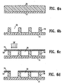
- the male mold (20) may be placed either above ( Figure 2a) or below ( Figure 2b) the web (24).
- the transparent conductive substrate is constructed by forming a transparent conductor film (21) on a glass plate or a plastic substrate. A layer of a thermoplastic or thermoset precursor (22) is then coated on the conductor film. The thermoplastic or thermoset precursor layer is embossed at a temperature higher than the glass transition temperature of the thermoplastic or thermoset precursor layer by the male mold in the form of a roller, plate or belt.
- the thermoplastic or thermoset precursor for the preparation of the microcups may be multifunctional acrylate or methacrylate, vinylether, epoxide and their oligomers, polymers and the like. Multifunctional acrylate and their oligomers are the most preferred. A combination of multifunctional epoxide and multifunctional acrylate is also very useful to achieve desirable physico-mechanical properties. A crosslinkable oligomer imparting flexibility, such as urethane acrylate or polyester acrylate, is usually also added to improve the flexure resistance of the embossed micro-cups.
- the composition may contain polymer, oligomer, monomer and additives or only oligomer, monomer and additives.
- the glass transition temperatures (or Tg) for this class of materials usually range from about -70°C to about 150°C, preferably from about -20°C to about 50°C.
- the microembossing process is typically carried out at a temperature higher than the Tg.
- a heated male mold or a heated housing substrate against which the mold presses may be used to control the microembossing temperature and pressure.
- the mold is released during or after the precursor layer is hardened to reveal an array of microcups (23).
- the hardening of the precursor layer may be accomplished by cooling, cross-linking by radiation, heat or moisture.
- UV radiation UV may radiate onto the transparent conductor film from the bottom or the top of the web as shown in the two figures.
- UV lamps may be placed inside the mold. In this case, the mold must be transparent to allow the UV light to radiate through the pre-patterned male mold on to the thermoset precursor layer.
- the male mold may be prepared by a photoresist process followed by either etching or electroplating.
- a representative example for the preparation of the male mold is given in Figure 3.
- a glass base (30) is sputtered with a thin layer (typically 3000 ⁇ ) of a seed metal (31) such as chrome inconel. It is then coated with a layer of photoresist (32) and exposed to UV.
- a mask (34) is placed between the UV and the layer of photoresist (32). The exposed areas of the photoresist become hardened. The unexposed areas are then removed by washing them with an appropriate solvent. The remaining hardened photoresist is dried and sputtered again with a thin layer of seed metal.
- a master ( Figure 3b) is then ready for electroforming.
- a typical material used for electroforming is nickel cobalt (33).
- the master can be made of nickel by nickel sulfamate electroforming or electroless nickel deposition as described in "Continuous manufacturing of thin cover sheet optical media", SPIE Proc. Vol. 1663, pp.324 (1992).
- the floor of the mold ( Figure 3d) is typically between 50 to 400 microns.
- the master can also be made using other microengineering techniques including e-beam writing, dry etching, chemical etching, laser writing or laser interference as described in "Replication techniques for micro-optics", SPIE Proc. Vol.3099, pp76-82 (1997).
- the mold can be made by photomachining using plastics, ceramics or metals.
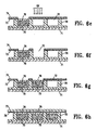
- the microcups may be prepared by imagewise exposure ( Figure 4a) of a radiation curable material (51) coated on the conductor film (52) to UV or other forms of radiation through a mask (50).
- the conductor film (52) is on a plastic substrate (53).
- the photomask may be synchronized with the web and move at the same speed as the latter.
- the dark squares (54) represent the opaque area and the space (55) between the dark squares represents the opening area.
- the UV radiates through the opening area (55) onto the radiation curable material.
- the exposed areas become hardened and the unexposed areas (protected by the opaque area in the mask) are then removed by an appropriate solvent or developer to form the microcups (56).
- the solvent or developer is selected from those commonly used for dissolving or reducing the viscosity of radiation curable materials such as methylethylketone, toluene, acetone, isopropanol or the like.
- Figures 4b and 4c illustrate two other options for the preparation of microcups by imagewise exposure.
- the conductor film (52) used is opaque and pre-patterned. In this case, it may be advantageous to imagewise expose the radiation sensitive material through the conductor pattern which serves as the photomask.
- the microcups (56) can then be formed by removing the unexposed areas after UV radiation.
- the conductor film (52) is also opaque and line-patterned. The radiation curable material is exposed from the bottom through the conductor line pattern (52) which serves as the first photomask. A second exposure is performed from the other side through the second photomask (50) having a line pattern perpendicular to the conductor lines.
- the unexposed area is then removed by a solvent or developer to reveal the microcups (56).
- the microcups can be of any shape, and their sizes and shapes may vary.
- the microcups may be of substantially uniform size and shape in one system.
- microcups having a mixture of different shapes and sizes may be produced.
- microcups filled with a dispersion of the red color may have a different shape or size from the green microcups or the blue microcups.
- a pixel may consist of different numbers of microcups of different colors.
- a pixel may consist of a number of small green microcups, a number of large red microcups, and a number of small blue microcups. It is not necessary to have the same shape and number for the three colors.
- the openings of the microcups may be round, square, rectangular, hexagonal, or any other shape.
- the partition area between the openings is preferably kept small in order to achieve a high color saturation and contrast while maintaining desirable mechanical properties. Consequently the honeycomb-shaped opening is preferred over, for example, the circular opening.
- each individual microcup may be in the range of about 10 2 to about 5x10 5 ⁇ m 2 , preferably from about 10 3 to about 5x10 4 ⁇ m 2 .
- the depth of the microcups is in the range of about 3 to about 100 microns, preferably from about 10 to about 50 microns.
- the opening to wall ratio is in the range of from about 0.05 to about 100, preferably from about 0.4 to about 20.
- the distances of the openings usually are in the range of from about 15 to about 450 microns, preferably from about 25 to about 300 microns from edge to edge of the openings.
- the microcups are filled with charged pigment particles dispersed in a dielectric solvent.
- the dispersion may be prepared according to methods well known in the art such as US Patent Nos. 6,017,584, 5,914,806, 5,573,711, 5,403,518, 5,380,362, 4,680,103, 4,285,801, 4,093,534, 4,071,430,3,668,106 and IEEE Trans . Electron Devices , ED-24, 827 (1977), and J . Appl . Phys . 49(9), 4820 (1978).
- the charged pigment particles visually contrast with the medium in which the particles are suspended.
- the medium is a dielectric solvent which preferably has a low viscosity and a dielectric constant in the range of about 2 to about 30, preferably about 2 to about 15 for high particle mobility.
- suitable dielectric solvents include hydrocarbons such as decahydronaphthalene (DECALIN), 5-ethylidene-2-norbornene, fatty oils, paraffin oil, aromatic hydrocarbons such as toluene, xylene, phenylxylylethane, dodecylbenzene and alkylnaphthalene, halogenated solvents such as perfluorodecalin, perfluorotoluene, perfluoroxylene, dichlorobenzotrifluoride, 3,4,5-trichlorobenzotrifluoride, chloropentafluoro-benzene, dichlorononane, pentachlorobenzene, and perfluoro solvents such as FC-43, FC-70 and FC-5060 from 3M Company, St.
- halogen containing polymers such as poly(perfluoropropylene oxide) from TCI America, Portland, Oregon, poly(chlorotrifluoroethylene) such as Halocarbon Oils from Halocarbon Product Corp., River Edge, NJ, perfluoropolyalkylether such as Galden from Ausimont or Krytox Oils and Greases K-Fluid Series from DuPont, Delaware.
- poly(chlorotrifluoroethylene) is used as the dielectric solvent.
- poly(perfluoropropylene oxide) is used as the dielectric solvent.
- the suspending medium may be colored by dyes or pigments.
- Nonionic azo and anthraquinone dyes are particularly useful. Examples of useful dyes include, but are not limited to: Oil Red EGN, Sudan Red, Sudan Blue, Oil Blue, Macrolex Blue, Solvent Blue 35, Pylam Spirit Black and Fast Spirit Black from Pylam Products Co., Arizona, Sudan Black B from Aldrich, Thermoplastic Black X-70 from BASF, anthroquinone blue, anthroquinone yellow 114, anthroquinone red 111, 135, anthroquinone green 28 from Aldrich.
- the pigment particles for generating the color of the medium may also be dispersed in the dielectric medium. These color particles are preferably uncharged.
- the pigment particles for generating color in the medium are charged, they preferably carry a charge which is opposite from that of the charged pigment particles. If both types of pigment particles carry the same charge, then they should have different charge density or different electrophoretic mobility. In any case, the dye or pigment for generating color of the medium must be chemically stable and compatible with other components in the suspension.
- the charged pigment particles may be organic or inorganic pigments, such as TiO 2 , phthalocyanine blue, phthalocyanine green, diarylide yellow, diarylide AAOT Yellow, and quinacridone, azo, rhodamine, perylene pigment series from Sun Chemical, Hansa yellow G particles from Kanto Chemical, and Carbon Lampblack from Fisher. Submicron particle size is preferred.
- the particles should have acceptable optical characteristics, should not be swollen or softened by the dielectric solvent, and should be chemically stable. The resulting suspension must also be stable against sedimentation, creaming or flocculation under normal operating conditions.
- the pigment particles may exhibit a native charge, or may be charged explicitly using a charge control agent, or may acquire a charge when suspended in the dielectric solvent.
- Suitable charge control agents are well known in the art; they may be polymeric or non-polymeric in nature, and may also be ionic or nonionic, including ionic surfactants such as Aerosol OT, sodium dodecylbenzenesulfonate, metal soap, polybutene succinimide, maleic anhydride copolymers, vinylpyridine copolymers, vinylpyrrolidone copolymer (such as Ganex from International Specialty Products), (meth)acrylic acid copolymers, N,N-dimethylaminoethyl (meth)acrylate copolymers.
- Fluorosurfactants are particularly useful as charge controlling agents in perfluorocarbon solvents. These include FC fluorosurfactants such as FC-170C, FC-171, FC-176, FC430, FC431 and FC-740 from 3M Company and Zonyl fluorosurfactants such as Zonyl FSA, FSE, FSN, FSN-100, FSO, FSO-100, FSD and UR from Dupont.
- FC fluorosurfactants such as FC-170C, FC-171, FC-176, FC430, FC431 and FC-740 from 3M Company
- Zonyl fluorosurfactants such as Zonyl FSA, FSE, FSN, FSN-100, FSO, FSO-100, FSD and UR from Dupont.
- Suitable charged pigment dispersions may be manufactured by any of the well-known methods including grinding, milling, attriting, microfluidizing, and ultrasonic techniques. For example, pigment particles in the form of a fine powder are added to the suspending solvent and the resulting mixture is ball milled or attrited for several hours to break up the highly agglomerated dry pigment powder into primary particles. Although less preferred, a dye or pigment for generating color of the suspending medium may be added to the suspension during the ball milling process.
- Sedimentation or creaming of the pigment particles may be eliminated by microencapsulating the particles with suitable polymers to match the specific gravity to that of the dielectric solvent.
- Microencapsulation of the pigment particles may be accomplished chemically or physically. Typical microencapsulation processes include interfacial polymerization, in-situ polymerization, phase separation, coacervation, electrostatic coating, spray drying, fluidized bed coating and solvent evaporation.
- the suspension comprises charged white particles of titanium oxide (TiO 2 ) dispersed in a black solvent or charged black particles dispersed in a dielectric solvent.
- a black dye or dye mixture such as Pylam Spirit Black and Fast Spirit Black from Pylam Products Co. Arizona, Sudan Black B from Aldrich, Thermoplastic Black X-70 from BASF, or an insoluble black pigment such as carbon black may be used to generate the black color of the solvent.
- the charged TiO 2 particles may be suspended in a dielectric solvent of cyan, yellow or magenta color. The cyan, yellow or magenta color may be generated via the use of a dye or a pigment.
- the charged TiO 2 particles may be suspended in a dielectric solvent of red, green or blue color generated also via the use of a dye or a pigment. The red, green, blue color system is preferred for most applications.
- the sealing of the microcups may be accomplished in a number of ways.
- a preferred approach is to disperse a UV curable composition containing multifunctional acrylates, acrylated oligomers, and photoinitiators into an electrophoretic fluid containing charged pigment particles dispersed in a colored dielectric solvent.
- the UV curable composition is immiscible with the dielectric solvent and has a specific gravity lower than that of the dielectric solvent and the pigment particles.
- the two components, UV curable composition and the electrophoretic fluid are thoroughly blended in an in-line mixer and immediately coated onto the microcups with a precision coating mechanism such as Myrad bar, gravure, doctor blade, slot coating or slit coating. Excess fluid is scraped away by a wiper blade or a similar device.
- a small amount of a weak solvent or solvent mixture such as isopropanol, methanol, or their aqueous solutions may be used to clean the residual electrophoretic fluid on the top surface of the partition walls of the microcups.
- Volatile organic solvents may be used to control the viscosity and coverage of the electrophoretic fluid.
- the thus-filled microcups are then dried and the UV curable composition floats to the top of the electrophoretic fluid.
- the microcups may be sealed by curing the supernatant UV curable layer during or after it floats to the top. UV or other forms of radiation such as visible light, IR and electron beam may be used to cure and seal the microcups. Alternatively, heat or moisture may also be employed to cure and seal the microcups, if appropriate, heat or moisture curable compositions may be used.
- a preferred group of dielectric solvents exhibiting desirable density and solubility discrimination against acrylate monomers and oligomers are halogenated hydrocarbons and their derivatives.
- Surfactants may be used to improve the adhesion and wetting at the interface between the electrophoretic fluid and the sealing materials.
- Useful surfactants include the FC surfactants from 3M Company, Zonyl fluorosurfactants from DuPont, fluoroacrylates, fluoromethacrylates, fluoro-substituted long chain alcohols, perfluoro-substituted long chain carboxylic acids and their derivatives.
- the electrophoretic fluid and the sealing precursor may be coated sequentially into the microcups, if the sealing precursor is at least partially compatible with the dielectric solvent.
- the sealing of the microcups may be accomplished by overcoating a thin layer of thermoset precursor which is curable by radiation, heat, moisture or interfacial reactions and curing on the surface of the filled microcups. Interfacial polymerization followed by UV curing is very beneficial to the sealing process. Intermixing between the electrophoretic layer and the overcoat is significantly suppressed by the formation of a thin barrier layer at the interface by interfacial polymerization.
- the sealing is then completed by a post curing step, preferably by UV radiation.
- the specific gravity of the overcoating is significantly lower than that of the electrophoretic fluid.
- Volatile organic solvents may be used to adjust the viscosity and the thickness of the coatings. When a volatile solvent is used in the overcoat, it is preferred that it is immiscible with the dielectric solvent.
- the two-step overcoating process is particularly useful when the dye used is at least partially soluble in the thermoset precursor.
- the process is illustrated by the flow diagram as shown in Figure 5. All microcups are filled with a suspension of the same color composition.
- the process can be a continuous roll-to-roll process comprising the following steps:
- the laminate adhesive may be post cured by radiation such as UV (68) through the top conductor film if the latter is transparent to the radiation.
- the finished product may be cut (69) after the lamination step.
- the preparation of the microcups described above can be conveniently replaced by the alternative procedure of imagewise exposing the conductor film coated with a thermoset precursor followed by removing the unexposed areas by an appropriate solvent.
- the sealing of the microcups may alternatively be accomplished by directly overcoating and curing a layer of the thermoset precursor composition over the surface of the electrophoretic fluid.
- additional steps are needed to generate microcups containing suspensions of different colors. These additional steps include (1) laminating the already formed microcups with a positively working dry-film photoresist consisting of at least a removable support such as PET-4851 from Saint-Gobain, Worcester, MA, a novolac positive photoresist such as Microposit S1818 from Shipley, and an alkali-developable adhesive layer such as a mixture of Nacor 72-8685 from National Starch and Carboset 515 from BF Goodrich; (2) selectively opening a certain amount of the microcups by imagewise exposing the photoresist, removing the removable support film, and developing the positive photoresist with a developer such as diluted Microposit 351 developer from Shipley; (3) filling the opened cups with the electrophoretic fluid containing charged white pigment (TiO 2 ) particles and dye or pigment of the first primary color; and (4) sealing the filled microcups as described in the preparation of monochrome displays
- a multi-color electrophoretic displays may be prepared according to the steps as shown in Figure 6:
- the preparation of the microcups described in the process above can conveniently be replaced by the alternative procedure of imagewise exposing the conductor film coated with a thermoset precursor followed by removing the unexposed areas by an appropriate solvent.
- the sealing of the microcups may be alternatively accomplished by directly coating a layer of the thermoset precursor material over the surface of the liquid phase.
- the thickness of the display produced by the present processes as described can be as thin as a piece of paper.
- the width of the display is the width of the coating web (typically 3-90 inches).
- the length of the display can be anywhere from inches to thousands of feet depending on the size of the roll.
- composition shown in Table 1 is coated onto Mylar J101/200 gauge using a Nickel Chrome bird type film applicator with an opening of 3 mil. The solvent is allowed to evaporate leaving behind a tacky film with a Tg below room temperature.
- the coated film was then embossed by the stencil using a pressure roller at room temperature.
- the coating was then UV cured for about 20 minutes through the Mylar film using a Loctite Zeta 7410 exposure unit equipped with a metal fluoride lamp with an intensity of 80 mW/cm 2 at 365 nm.
- the embossed film was then released from the mold to reveal well-defined microcups having lateral dimensions ranging from 60 ⁇ m to 120 ⁇ m (200-400 dpi) and a depth ranging from 5 ⁇ m to 30 ⁇ m as measured by optical profilometry and microscope
- a composition containing solid oligomer, monomer and additive is shown in Table 2.
- the glass transition temperature of the mixture is again below room temperature.
- the tacky coating is deposited on top of Mylar J101/200 gauge as before.
- Embossing can be conducted at 32°C and 60°C using a heated pressure roller or laminator. Well-defined high resolution microcups (100-400 dpi) with depth ranging from 5-30 microns were produced.
- Polystyrene (0.89 grams, Polysciences, Inc., mw. 50,000) and AOT (0.094 grams, American Cyanamide, sodium dioctylsulfosuccinate) were dissolved in 17.77 grams of hot xylene (Aldrich).
- Ti-Pure R-706 (6.25 grams) was added to the solution and ground in an attritor at 200 rpm for more than 12 hours. A low viscosity, stable dispersion was obtained.
- Oil-blue N (0.25 grams, Aldrich) was added to color the dispersion. The suspension was then tested in a standard electrophoretic cell comprising two ITO conductor plates separated by a 24 microns spacer. High contrast, alternating white and blue images were observed with a switching rate of about 60 Hz and a rising time of 8.5 msec at 80 volts.
- Example 3 The experiment of Example 3 was repeated, except Oil Red EGN (Aldrich) and an electrophoretic cell with a 24 micron spacer were used. High contrast, alternating red and white images were observed with a switching rate of 60 Hz and a rising time of 12 msec at 60 volts.
- Oil Red EGN Aldrich
- an electrophoretic cell with a 24 micron spacer were used. High contrast, alternating red and white images were observed with a switching rate of 60 Hz and a rising time of 12 msec at 60 volts.
- Ti-Pure R-706 (112 grams) was ground by an attritor in a solution containing 11.2 grams of a maleic anhydride copolymer (Baker Hughes X-5231), 24 grams of 3,4-dichlorobenzotrifluoride, and 24 grams of 1,6-dichlorohexane (both from Aldrich). Similarly, 12 grams of carbon black were ground in a solution containing 1.2 grams of alkylated polyvinylpyrrolidone (Ganex V216 from ISP), 34 grams of 3,4-dichlorobenzotrifluoride, and 34 grams of 1,6-dichlorohexane (Aldrich) at 100 °C. These two dispersions were then mixed homogeneously and tested. High contrast black and white images were observed with a switching rate up to 10 Hz and a rising time of about 36 msec at 100 volts.
- UV curable composition comprising 1 wt% ofbenzil dimethyl ketal (Esacure KB1 from Sartomer) in HDDA (1,6-hexanediol diacrylate from Aldrich) were dispersed into 0.4 ml of a dielectric solvent comprising 0.5 wt% of 2,2,3,3,4,4,5,5,6,6,7,7,8,8,9,9,10,10,10-nonadccafluoro-1-decanol (Aldrich) in FC-43 from 3M Company. The resultant dispersion was then immediately filled into an array of microcups as prepared in Example 2. Excess of fluid was scrapped away by a wiper blade. The HDDA solution was allowed to phase separate for at least 30 seconds and cured by UV radiation (10 mw/cm 2 ) for about 1 minute. A hard, clear layer was observed on the top of the microcups and the microcups were sealed.
- the elctrophoretic fluid prepared in Example 5 was coated onto the microcup array as prepared in Example 2.
- a thin layer of Norland optical adhesive NOA 60 Norland Products Inc., New Brunswick, NJ was coated onto the filled microcups. Any excess of the UV adhesive was scrapped off by a strip of Mylar film and cleaned by a piece of absorbing paper.
- the overcoated adhesive was then cured immediately under a Loctite Zeta 7410 UV exposure unit for about 15 minutes. The microcups were sealed completely and no air pocket was observed.
- the thickness of cured adhesive layer was about 5-10 microns as measured by a Mitutoyo thickness gauge.
- Example 7 The experiment of Example 7 was repeated, except the Norland adhesive was replaced by Instant Krazy glue from Elmer's Products, Inc., Columbus, Ohio. The overcoated adhesive was then cured for 5 minutes by moisture in air. The microcups were sealed completely and no air pocket was observed. The thickness of cured adhesive layer was about 5-10 microns as measured by a Mitutoyo thickness gauge.
- Example 8 The experiment of Example 8 was repeated, except the electrophoretic fluid was replaced by a 3,4-dichlorobenzotrifluoride solution containing 0.3 wt% of tetraethylenepentaamine (Aldrich) and the Instant Krazy glue was replaced by an aliphatic polyisocyanate (Desmodur N 3300 from Bayer Corp.) solution in anhydrous ether. A highly crosslinked thin film was observed almost immediately after overcoating. The dielectric solvent was completely sealed inside the microcups after ether was evaporated at room temperature. No air pocket was observed.
Landscapes
- Physics & Mathematics (AREA)
- Nonlinear Science (AREA)
- Optics & Photonics (AREA)
- General Physics & Mathematics (AREA)
- Chemical & Material Sciences (AREA)
- Electrochemistry (AREA)
- Molecular Biology (AREA)
- Health & Medical Sciences (AREA)
- Chemical Kinetics & Catalysis (AREA)
- Life Sciences & Earth Sciences (AREA)
- Mathematical Physics (AREA)
- Crystallography & Structural Chemistry (AREA)
- Electrochromic Elements, Electrophoresis, Or Variable Reflection Or Absorption Elements (AREA)
- Eye Examination Apparatus (AREA)
- Processes Of Treating Macromolecular Substances (AREA)
- Devices For Indicating Variable Information By Combining Individual Elements (AREA)
Priority Applications (1)
| Application Number | Priority Date | Filing Date | Title |
|---|---|---|---|
| EP04025496A EP1500970A1 (en) | 2000-03-03 | 2001-03-05 | Electrophoretic display |
Applications Claiming Priority (3)
| Application Number | Priority Date | Filing Date | Title |
|---|---|---|---|
| US09/518,488 US6930818B1 (en) | 2000-03-03 | 2000-03-03 | Electrophoretic display and novel process for its manufacture |
| US518488 | 2000-03-03 | ||
| PCT/US2001/006917 WO2001067170A1 (en) | 2000-03-03 | 2001-03-05 | Electrophoretic display |
Related Child Applications (1)
| Application Number | Title | Priority Date | Filing Date |
|---|---|---|---|
| EP04025496A Division EP1500970A1 (en) | 2000-03-03 | 2001-03-05 | Electrophoretic display |
Publications (2)
| Publication Number | Publication Date |
|---|---|
| EP1264210A1 EP1264210A1 (en) | 2002-12-11 |
| EP1264210B1 true EP1264210B1 (en) | 2004-11-24 |
Family
ID=24064141
Family Applications (2)
| Application Number | Title | Priority Date | Filing Date |
|---|---|---|---|
| EP01914676A Expired - Lifetime EP1264210B1 (en) | 2000-03-03 | 2001-03-05 | Electrophoretic display |
| EP04025496A Withdrawn EP1500970A1 (en) | 2000-03-03 | 2001-03-05 | Electrophoretic display |
Family Applications After (1)
| Application Number | Title | Priority Date | Filing Date |
|---|---|---|---|
| EP04025496A Withdrawn EP1500970A1 (en) | 2000-03-03 | 2001-03-05 | Electrophoretic display |
Country Status (13)
Cited By (1)
| Publication number | Priority date | Publication date | Assignee | Title |
|---|---|---|---|---|
| DE102005004156A1 (de) * | 2005-01-28 | 2006-08-10 | Siemens Ag | Elektrophoretische Displayfolie |
Families Citing this family (376)
| Publication number | Priority date | Publication date | Assignee | Title |
|---|---|---|---|---|
| US7167155B1 (en) | 1995-07-20 | 2007-01-23 | E Ink Corporation | Color electrophoretic displays |
| DE69636960C5 (de) * | 1996-07-19 | 2015-07-30 | E-Ink Corp. | Elektronisch adressierbare mikroverkapselte Tinte |
| US6839158B2 (en) | 1997-08-28 | 2005-01-04 | E Ink Corporation | Encapsulated electrophoretic displays having a monolayer of capsules and materials and methods for making the same |
| US7075502B1 (en) | 1998-04-10 | 2006-07-11 | E Ink Corporation | Full color reflective display with multichromatic sub-pixels |
| AU3987299A (en) | 1998-05-12 | 1999-11-29 | E-Ink Corporation | Microencapsulated electrophoretic electrostatically-addressed media for drawing device applications |
| US6930818B1 (en) | 2000-03-03 | 2005-08-16 | Sipix Imaging, Inc. | Electrophoretic display and novel process for its manufacture |
| US6933098B2 (en) | 2000-01-11 | 2005-08-23 | Sipix Imaging Inc. | Process for roll-to-roll manufacture of a display by synchronized photolithographic exposure on a substrate web |
| US7576904B2 (en) * | 2000-03-03 | 2009-08-18 | Sipix Imaging, Inc. | Electro-magnetophoresis display |
| US6829078B2 (en) * | 2000-03-03 | 2004-12-07 | Sipix Imaging Inc. | Electrophoretic display and novel process for its manufacture |
| US20070237962A1 (en) | 2000-03-03 | 2007-10-11 | Rong-Chang Liang | Semi-finished display panels |
| US7408696B2 (en) | 2000-03-03 | 2008-08-05 | Sipix Imaging, Inc. | Three-dimensional electrophoretic displays |
| US7715087B2 (en) | 2000-03-03 | 2010-05-11 | Sipix Imaging, Inc. | Segment electrophoretic displays and methods for their manufacture |
| US7557981B2 (en) | 2000-03-03 | 2009-07-07 | Sipix Imaging, Inc. | Electrophoretic display and process for its manufacture |
| US6831770B2 (en) * | 2000-03-03 | 2004-12-14 | Sipix Imaging, Inc. | Electrophoretic display and novel process for its manufacture |
| US7233429B2 (en) | 2000-03-03 | 2007-06-19 | Sipix Imaging, Inc. | Electrophoretic display |
| US6972893B2 (en) | 2001-06-11 | 2005-12-06 | Sipix Imaging, Inc. | Process for imagewise opening and filling color display components and color displays manufactured thereof |
| US7052571B2 (en) | 2000-03-03 | 2006-05-30 | Sipix Imaging, Inc. | Electrophoretic display and process for its manufacture |
| US6865012B2 (en) | 2000-03-03 | 2005-03-08 | Sipix Imaging, Inc. | Electrophoretic display and novel process for its manufacture |
| US6947202B2 (en) | 2000-03-03 | 2005-09-20 | Sipix Imaging, Inc. | Electrophoretic display with sub relief structure for high contrast ratio and improved shear and/or compression resistance |
| US6885495B2 (en) | 2000-03-03 | 2005-04-26 | Sipix Imaging Inc. | Electrophoretic display with in-plane switching |
| US7158282B2 (en) | 2000-03-03 | 2007-01-02 | Sipix Imaging, Inc. | Electrophoretic display and novel process for its manufacture |
| US7715088B2 (en) | 2000-03-03 | 2010-05-11 | Sipix Imaging, Inc. | Electrophoretic display |
| US7142351B2 (en) * | 2000-03-03 | 2006-11-28 | Sipix Imaging, Inc. | Electro-magnetophoresis display |
| US6545797B2 (en) | 2001-06-11 | 2003-04-08 | Sipix Imaging, Inc. | Process for imagewise opening and filling color display components and color displays manufactured thereof |
| NL1015841C2 (nl) * | 2000-07-31 | 2002-02-01 | Zetfolie B V | Een systeem voor beeldvorming alsmede een inrichting en werkwijze om dit systeem te regelen. |
| US6795138B2 (en) | 2001-01-11 | 2004-09-21 | Sipix Imaging, Inc. | Transmissive or reflective liquid crystal display and novel process for its manufacture |
| US8282762B2 (en) * | 2001-01-11 | 2012-10-09 | Sipix Imaging, Inc. | Transmissive or reflective liquid crystal display and process for its manufacture |
| US7471369B2 (en) * | 2001-01-11 | 2008-12-30 | Sipix Imaging, Inc. | Transmissive or reflective liquid crystal display and process for its manufacture |
| TW556044B (en) | 2001-02-15 | 2003-10-01 | Sipix Imaging Inc | Process for roll-to-roll manufacture of a display by synchronized photolithographic exposure on a substrate web |
| US7604706B2 (en) * | 2001-03-30 | 2009-10-20 | Minolta Co., Ltd. | Method for producing resin-molded substrate and method for producing reversible image display medium |
| US7230750B2 (en) * | 2001-05-15 | 2007-06-12 | E Ink Corporation | Electrophoretic media and processes for the production thereof |
| US6753067B2 (en) | 2001-04-23 | 2004-06-22 | Sipix Imaging, Inc. | Microcup compositions having improved flexure resistance and release properties |
| US8361356B2 (en) * | 2001-06-04 | 2013-01-29 | Sipix Imaging, Inc. | Composition and process for the sealing of microcups in roll-to-roll display manufacturing |
| US7205355B2 (en) | 2001-06-04 | 2007-04-17 | Sipix Imaging, Inc. | Composition and process for the manufacture of an improved electrophoretic display |
| US20020188053A1 (en) | 2001-06-04 | 2002-12-12 | Sipix Imaging, Inc. | Composition and process for the sealing of microcups in roll-to-roll display manufacturing |
| US7385751B2 (en) | 2001-06-11 | 2008-06-10 | Sipix Imaging, Inc. | Process for imagewise opening and filling color display components and color displays manufactured thereof |
| US6788452B2 (en) | 2001-06-11 | 2004-09-07 | Sipix Imaging, Inc. | Process for manufacture of improved color displays |
| US6982178B2 (en) * | 2002-06-10 | 2006-01-03 | E Ink Corporation | Components and methods for use in electro-optic displays |
| TW527529B (en) * | 2001-07-27 | 2003-04-11 | Sipix Imaging Inc | An improved electrophoretic display with color filters |
| JP4155553B2 (ja) * | 2001-08-01 | 2008-09-24 | キヤノン株式会社 | 表示素子及びその製造方法 |
| US7492505B2 (en) * | 2001-08-17 | 2009-02-17 | Sipix Imaging, Inc. | Electrophoretic display with dual mode switching |
| US7038670B2 (en) * | 2002-08-16 | 2006-05-02 | Sipix Imaging, Inc. | Electrophoretic display with dual mode switching |
| TW550529B (en) | 2001-08-17 | 2003-09-01 | Sipix Imaging Inc | An improved electrophoretic display with dual-mode switching |
| TW539928B (en) | 2001-08-20 | 2003-07-01 | Sipix Imaging Inc | An improved transflective electrophoretic display |
| TW573204B (en) | 2001-09-12 | 2004-01-21 | Sipix Imaging Inc | An improved electrophoretic display with gating electrodes |
| TWI229763B (en) | 2001-10-29 | 2005-03-21 | Sipix Imaging Inc | An improved electrophoretic display with holding electrodes |
| TWI250894B (en) * | 2002-01-03 | 2006-03-11 | Sipix Imaging Inc | Functionalized halogenated polymers for microencapsulation |
| TWI229776B (en) | 2002-01-03 | 2005-03-21 | Sipix Imaging Inc | A novel electrophoretic dispersion with a fluorinated solvent and a charge controlling agent |
| US6529313B1 (en) * | 2002-01-16 | 2003-03-04 | Xerox Corporation | Electrophoretic displays, display fluids for use therein, and methods of displaying images |
| US6525866B1 (en) * | 2002-01-16 | 2003-02-25 | Xerox Corporation | Electrophoretic displays, display fluids for use therein, and methods of displaying images |
| US7123238B2 (en) * | 2002-01-16 | 2006-10-17 | Xerox Corporation | Spacer layer for electrophoretic display device |
| US7382514B2 (en) * | 2002-02-11 | 2008-06-03 | Sipix Imaging, Inc. | Core-shell particles for electrophoretic display |
| US6885146B2 (en) * | 2002-03-14 | 2005-04-26 | Semiconductor Energy Laboratory Co., Ltd. | Display device comprising substrates, contrast medium and barrier layers between contrast medium and each of substrates |
| TW578121B (en) | 2002-03-21 | 2004-03-01 | Sipix Imaging Inc | Magnetophoretic and electromagnetophoretic display |
| US7580180B2 (en) | 2002-03-21 | 2009-08-25 | Sipix Imaging, Inc. | Magnetophoretic and electromagnetophoretic displays |
| US7113323B2 (en) | 2002-03-21 | 2006-09-26 | Sipix Imaging, Inc. | Magnetophoretic and electromagnetophoretic displays |
| CN1209674C (zh) | 2002-04-23 | 2005-07-06 | 希毕克斯影像有限公司 | 电磁泳显示器 |
| TWI223729B (en) | 2002-04-23 | 2004-11-11 | Sipix Imaging Inc | Improved segment electrophoretic displays and methods for their manufacture |
| TWI240842B (en) | 2002-04-24 | 2005-10-01 | Sipix Imaging Inc | Matrix driven electrophoretic display with multilayer back plane |
| US7261920B2 (en) * | 2002-04-24 | 2007-08-28 | Sipix Imaging, Inc. | Process for forming a patterned thin film structure on a substrate |
| TWI268813B (en) * | 2002-04-24 | 2006-12-21 | Sipix Imaging Inc | Process for forming a patterned thin film conductive structure on a substrate |
| US7156945B2 (en) | 2002-04-24 | 2007-01-02 | Sipix Imaging, Inc. | Process for forming a patterned thin film structure for in-mold decoration |
| US8002948B2 (en) * | 2002-04-24 | 2011-08-23 | Sipix Imaging, Inc. | Process for forming a patterned thin film structure on a substrate |
| TW574538B (en) * | 2002-04-24 | 2004-02-01 | Sipix Imaging Inc | Compositions and processes for format flexible roll-to-roll manufacturing of electrophoretic displays |
| US7307778B2 (en) | 2002-04-24 | 2007-12-11 | Sipix Imaging, Inc. | Compositions and processes for format-flexible, roll-to-roll manufacturing of electrophoretic displays |
| US7972472B2 (en) * | 2002-04-24 | 2011-07-05 | Sipix Imaging, Inc. | Process for forming a patterned thin film structure for in-mold decoration |
| TWI310098B (en) * | 2002-05-03 | 2009-05-21 | Sipix Imaging Inc | Methods of surface modification for improving electrophoretic display performance |
| TWI329662B (en) | 2002-05-17 | 2010-09-01 | Sipix Imaging Inc | Novel fluorinated silicon (iv) phthalocyanines and naphthalocyanines for electrophoretic, magnetophoretic or electromagnetophoretic display |
| TW583497B (en) * | 2002-05-29 | 2004-04-11 | Sipix Imaging Inc | Electrode and connecting designs for roll-to-roll format flexible display manufacturing |
| DE60304945T2 (de) * | 2002-07-16 | 2007-01-04 | Seiko Epson Corp. | Mikrokapselhaltige Zusammensetzung für elektrophoretische Anzeigen |
| TWI314237B (en) * | 2002-07-17 | 2009-09-01 | Sipix Imaging Inc | Novel methods and compositions for improved electrophoretic display performance |
| US20060255322A1 (en) * | 2002-07-17 | 2006-11-16 | Wu Zarng-Arh G | Methods and compositions for improved electrophoretic display performance |
| US8547628B2 (en) | 2002-07-17 | 2013-10-01 | Sipix Imaging, Inc. | Methods and compositions for improved electrophoretic display performance |
| US7347957B2 (en) * | 2003-07-10 | 2008-03-25 | Sipix Imaging, Inc. | Methods and compositions for improved electrophoretic display performance |
| JP2005534996A (ja) * | 2002-08-06 | 2005-11-17 | イー−インク コーポレイション | 熱影響に対する電気光学表示装置の保護 |
| US7271947B2 (en) | 2002-08-16 | 2007-09-18 | Sipix Imaging, Inc. | Electrophoretic display with dual-mode switching |
| US7038656B2 (en) | 2002-08-16 | 2006-05-02 | Sipix Imaging, Inc. | Electrophoretic display with dual-mode switching |
| JP4337439B2 (ja) | 2002-08-22 | 2009-09-30 | セイコーエプソン株式会社 | 電気泳動装置、電子機器 |
| US7166182B2 (en) * | 2002-09-04 | 2007-01-23 | Sipix Imaging, Inc. | Adhesive and sealing layers for electrophoretic displays |
| TW575646B (en) * | 2002-09-04 | 2004-02-11 | Sipix Imaging Inc | Novel adhesive and sealing layers for electrophoretic displays |
| TWI300157B (en) * | 2002-09-10 | 2008-08-21 | Sipix Imaging Inc | Electrochromic or electrodeposition display and process for their preparation |
| TWI328711B (en) * | 2002-09-18 | 2010-08-11 | Sipix Imaging Inc | Electrophoretic display with improved temperature latitude and switching performance |
| US7616374B2 (en) * | 2002-09-23 | 2009-11-10 | Sipix Imaging, Inc. | Electrophoretic displays with improved high temperature performance |
| TWI327251B (en) * | 2002-09-23 | 2010-07-11 | Sipix Imaging Inc | Electrophoretic displays with improved high temperature performance |
| TWI293715B (en) * | 2002-10-10 | 2008-02-21 | Sipix Imaging Inc | A method for inducing or enhancing the threshold of an electrophoretic display, an electrophoretic fluid and an electrophoretic display |
| US20130063333A1 (en) | 2002-10-16 | 2013-03-14 | E Ink Corporation | Electrophoretic displays |
| US7245417B2 (en) * | 2002-10-21 | 2007-07-17 | Canon Kabushiki Kaisha | Process for producing display device |
| JP3927897B2 (ja) * | 2002-10-21 | 2007-06-13 | キヤノン株式会社 | 表示素子の製造方法 |
| TWI229230B (en) * | 2002-10-31 | 2005-03-11 | Sipix Imaging Inc | An improved electrophoretic display and novel process for its manufacture |
| TWI297089B (en) | 2002-11-25 | 2008-05-21 | Sipix Imaging Inc | A composition for the preparation of microcups used in a liquid crystal display, a liquid crystal display comprising two or more layers of microcup array and process for its manufacture |
| US8023071B2 (en) * | 2002-11-25 | 2011-09-20 | Sipix Imaging, Inc. | Transmissive or reflective liquid crystal display |
| US6831771B2 (en) | 2003-01-08 | 2004-12-14 | Sipix Imaging Inc. | Electronic whiteboard using electrophoretic display |
| WO2004066023A1 (en) * | 2003-01-17 | 2004-08-05 | Koninklijke Philips Electronics N.V. | Electrophoretic display |
| US7572491B2 (en) * | 2003-01-24 | 2009-08-11 | Sipix Imaging, Inc. | Adhesive and sealing layers for electrophoretic displays |
| TWI230832B (en) * | 2003-01-24 | 2005-04-11 | Sipix Imaging Inc | Novel adhesive and sealing layers for electrophoretic displays |
| US9346987B2 (en) * | 2003-01-24 | 2016-05-24 | E Ink California, Llc | Adhesive and sealing layers for electrophoretic displays |
| TWI337679B (en) | 2003-02-04 | 2011-02-21 | Sipix Imaging Inc | Novel compositions and assembly process for liquid crystal display |
| TWI228632B (en) * | 2003-02-06 | 2005-03-01 | Sipix Imaging Inc | Improved electrophoretic display with a bi-modal particle system |
| EP1631857B1 (en) * | 2003-06-06 | 2007-03-07 | Sipix Imaging, Inc. | In mold manufacture of an object with embedded display panel |
| ATE356368T1 (de) * | 2003-06-06 | 2007-03-15 | Sipix Imaging Inc | In-form-herstellung eines objekts mit eingebetteter anzeigetafel |
| KR20060012662A (ko) * | 2003-06-13 | 2006-02-08 | 코닌클리케 필립스 일렉트로닉스 엔.브이. | 전기이동 디스플레이 디바이스와 이러한 디바이스를제조하기 위한 방법 |
| US7390901B2 (en) * | 2003-08-08 | 2008-06-24 | Sipix Imaging, Inc. | Fluorinated dyes or colorants and their uses |
| EP1666965A4 (en) * | 2003-09-12 | 2006-11-08 | Bridgestone Corp | METHOD FOR PRODUCING IMAGE DISPLAY PANEL AND DISPLAY PANEL THEREFOR |
| US7061662B2 (en) * | 2003-10-07 | 2006-06-13 | Sipix Imaging, Inc. | Electrophoretic display with thermal control |
| US8514168B2 (en) * | 2003-10-07 | 2013-08-20 | Sipix Imaging, Inc. | Electrophoretic display with thermal control |
| US7177066B2 (en) | 2003-10-24 | 2007-02-13 | Sipix Imaging, Inc. | Electrophoretic display driving scheme |
| US7277218B2 (en) | 2003-11-04 | 2007-10-02 | Sipix Imaging, Inc. | Electrophoretic compositions |
| US7572394B2 (en) | 2003-11-04 | 2009-08-11 | Sipix Imaging, Inc. | Electrophoretic dispersions |
| US8257614B2 (en) | 2003-11-04 | 2012-09-04 | Sipix Imaging, Inc. | Electrophoretic dispersions |
| US8177942B2 (en) * | 2003-11-05 | 2012-05-15 | E Ink Corporation | Electro-optic displays, and materials for use therein |
| US20110164301A1 (en) | 2003-11-05 | 2011-07-07 | E Ink Corporation | Electro-optic displays, and materials for use therein |
| US8928562B2 (en) * | 2003-11-25 | 2015-01-06 | E Ink Corporation | Electro-optic displays, and methods for driving same |
| US7279064B2 (en) | 2003-12-18 | 2007-10-09 | Palo Alto Research Center, Incorporated | Method of sealing an array of cell microstructures using microencapsulated adhesive |
| CN100350323C (zh) * | 2003-12-29 | 2007-11-21 | 漳立冰 | 柔性超薄电泳显示屏及其制备方法 |
| US7504050B2 (en) * | 2004-02-23 | 2009-03-17 | Sipix Imaging, Inc. | Modification of electrical properties of display cells for improving electrophoretic display performance |
| US7980909B2 (en) * | 2004-04-08 | 2011-07-19 | Liquavista B.V. | Display device |
| US7470386B2 (en) | 2004-04-26 | 2008-12-30 | Sipix Imaging, Inc. | Roll-to-roll embossing tools and processes |
| US8625188B2 (en) * | 2004-05-12 | 2014-01-07 | Sipix Imaging, Inc. | Process for the manufacture of electrophoretic displays |
| US7374634B2 (en) * | 2004-05-12 | 2008-05-20 | Sipix Imaging, Inc. | Process for the manufacture of electrophoretic displays |
| CN1957290A (zh) * | 2004-05-28 | 2007-05-02 | 皇家飞利浦电子股份有限公司 | 柔性平板显示器 |
| CA2568421C (fr) * | 2004-07-02 | 2016-05-24 | Essilor International(Compagnie Generale D'optique) | Procede de realisation d'un element optique transparent, composant optique intervenant dans ce procede et element optique ainsi obtenu |
| US7301693B2 (en) * | 2004-08-13 | 2007-11-27 | Sipix Imaging, Inc. | Direct drive display with a multi-layer backplane and process for its manufacture |
| KR100616132B1 (ko) | 2004-08-24 | 2006-08-28 | 재단법인 전라남도신소재산업진흥재단 | 전기영동 디스플레이 장치용 격벽구조 및 그 구조를이용한 전기영동 디스플레이 장치 |
| US8643595B2 (en) * | 2004-10-25 | 2014-02-04 | Sipix Imaging, Inc. | Electrophoretic display driving approaches |
| US7304780B2 (en) * | 2004-12-17 | 2007-12-04 | Sipix Imaging, Inc. | Backplane design for display panels and processes for their manufacture |
| US7463409B2 (en) * | 2004-12-20 | 2008-12-09 | Palo Alto Research Center Incorporated | Flexible electrophoretic-type display |
| US20060146232A1 (en) * | 2004-12-31 | 2006-07-06 | Chi-Chang Liao | Passive matrix display and manufacture method |
| US8576162B2 (en) * | 2005-03-14 | 2013-11-05 | Sipix Imaging, Inc. | Manufacturing processes of backplane for segment displays |
| GB2425611B (en) | 2005-03-29 | 2010-03-24 | Hewlett Packard Development Co | Reflective colour display device |
| US7821700B2 (en) * | 2005-03-31 | 2010-10-26 | Mark W Miles | Dynamic motile medium |
| US8159636B2 (en) * | 2005-04-08 | 2012-04-17 | Sipix Imaging, Inc. | Reflective displays and processes for their manufacture |
| US20060280912A1 (en) * | 2005-06-13 | 2006-12-14 | Rong-Chang Liang | Non-random array anisotropic conductive film (ACF) and manufacturing processes |
| US8802214B2 (en) | 2005-06-13 | 2014-08-12 | Trillion Science, Inc. | Non-random array anisotropic conductive film (ACF) and manufacturing processes |
| US7248411B2 (en) * | 2005-06-24 | 2007-07-24 | Industrial Technology Research Institute | Optical film with array of microstructures and the light source apparatus utilizing the same |
| FR2888950B1 (fr) * | 2005-07-20 | 2007-10-12 | Essilor Int | Composant optique transparent pixellise a parois absordantes son procede de fabrication et son utilisation dans la farication d'un element optique transparent |
| FR2888948B1 (fr) * | 2005-07-20 | 2007-10-12 | Essilor Int | Composant optique transparent pixellise comprenant un revetement absorbant, son procede de realisation et son utilisation dans un element optique |
| FR2888947B1 (fr) | 2005-07-20 | 2007-10-12 | Essilor Int | Composant optique a cellules |
| KR100686870B1 (ko) * | 2005-09-07 | 2007-02-26 | 엘지전자 주식회사 | 오프셋 인쇄법을 이용한 전자종이 표시소자의 제조방법 |
| US7880958B2 (en) * | 2005-09-23 | 2011-02-01 | Sipix Imaging, Inc. | Display cell structure and electrode protecting layer compositions |
| US8441432B2 (en) * | 2005-09-23 | 2013-05-14 | Sipix Imaging, Inc. | Display cell structure and electrode protecting layer compositions |
| US7408699B2 (en) * | 2005-09-28 | 2008-08-05 | Sipix Imaging, Inc. | Electrophoretic display and methods of addressing such display |
| JP4586711B2 (ja) * | 2005-11-09 | 2010-11-24 | セイコーエプソン株式会社 | 電気泳動表示シートの製造方法および電気泳動表示装置の製造方法 |
| JP5194355B2 (ja) * | 2005-11-25 | 2013-05-08 | 富士ゼロックス株式会社 | 表示媒体及び表示方法 |
| JP2007147829A (ja) * | 2005-11-25 | 2007-06-14 | Brother Ind Ltd | 電気泳動表示媒体における隔壁及び基板の製造方法、及び、電気泳動表示媒体 |
| TWI271390B (en) * | 2005-12-13 | 2007-01-21 | Ind Tech Res Inst | Non-mask micro-flow etching process |
| JP2007218990A (ja) * | 2006-02-14 | 2007-08-30 | Toppan Forms Co Ltd | 電気泳動ディスプレイシステム |
| US7324264B2 (en) * | 2006-02-23 | 2008-01-29 | Eastman Kodak Company | Electro-optical modulating display and method of making the same |
| US7746541B2 (en) * | 2006-03-13 | 2010-06-29 | Honeywell International Inc. | System and apparatus for an electrophoretic display |
| US7982479B2 (en) * | 2006-04-07 | 2011-07-19 | Sipix Imaging, Inc. | Inspection methods for defects in electrophoretic display and related devices |
| KR101298296B1 (ko) * | 2006-05-08 | 2013-08-20 | 엘지디스플레이 주식회사 | 평판표시장치의 제조 방법 |
| US7280266B1 (en) * | 2006-05-19 | 2007-10-09 | Xerox Corporation | Electrophoretic display medium and device |
| US20070268446A1 (en) * | 2006-05-22 | 2007-11-22 | Shie-Chang Jeng | Liquid crystal device and method for forming the same |
| US7685967B2 (en) | 2006-05-23 | 2010-03-30 | Seed Resources, Llc | Feed cake assembly |
| US7683606B2 (en) * | 2006-05-26 | 2010-03-23 | Sipix Imaging, Inc. | Flexible display testing and inspection |
| JP2008008880A (ja) * | 2006-06-02 | 2008-01-17 | Sumitomo Bakelite Co Ltd | プラスチック製マイクロチップ、及びその製造方法、並びにそれを利用したバイオチップ又はマイクロ分析チップ |
| CN100412677C (zh) * | 2006-06-12 | 2008-08-20 | 天津大学 | 微格法电泳显示器的制备方法 |
| US8830561B2 (en) | 2006-07-18 | 2014-09-09 | E Ink California, Llc | Electrophoretic display |
| US20080020007A1 (en) * | 2006-07-18 | 2008-01-24 | Zang Hongmei | Liquid-containing film structure |
| US20150005720A1 (en) | 2006-07-18 | 2015-01-01 | E Ink California, Llc | Electrophoretic display |
| US7307779B1 (en) | 2006-09-21 | 2007-12-11 | Honeywell International, Inc. | Transmissive E-paper display |
| US8623191B2 (en) * | 2006-09-22 | 2014-01-07 | Honeywell International Inc. | Non-volatile addressable electronic paper with gray level capability |
| US7923488B2 (en) * | 2006-10-16 | 2011-04-12 | Trillion Science, Inc. | Epoxy compositions |
| DE102006052606B4 (de) | 2006-11-08 | 2008-09-18 | Leonhard Kurz Gmbh & Co. Kg | Verfahren zur Herstellung von PDLCDs |
| US7675672B2 (en) * | 2006-11-09 | 2010-03-09 | Honeywell International Inc. | Non-volatile addressable electronic paper for disposable flexible displays |
| US7843623B2 (en) * | 2006-11-16 | 2010-11-30 | Honeywell International Inc. | Non volatile addressable electronic paper with color capability |
| US7905977B2 (en) * | 2006-11-17 | 2011-03-15 | Sipix Imaging, Inc. | Post conversion methods for display devices |
| FR2910642B1 (fr) * | 2006-12-26 | 2009-03-06 | Essilor Int | Composant optique transparent a deux ensembles de cellules |
| US8011592B2 (en) * | 2007-01-19 | 2011-09-06 | Sipix Imaging, Inc. | Temperature management in an integrated circuit card with electrophoretic display |
| JP4906539B2 (ja) * | 2007-03-02 | 2012-03-28 | 株式会社リコー | ハニカム構造物、ハニカム構造物の製造方法及び画像表示装置 |
| US7936498B2 (en) * | 2007-03-08 | 2011-05-03 | Ricoh Company, Ltd. | Display element, image display device, and image display system |
| JP5157200B2 (ja) * | 2007-03-08 | 2013-03-06 | 株式会社リコー | ハニカム構造シートの製造方法及び表示パネルの製造方法 |
| JP5132168B2 (ja) * | 2007-03-08 | 2013-01-30 | 株式会社リコー | 画像表示素子用構造体の製造方法及び製造装置、並びに電気泳動表示素子の製造方法及び製造装置 |
| US8274472B1 (en) | 2007-03-12 | 2012-09-25 | Sipix Imaging, Inc. | Driving methods for bistable displays |
| JP2007179079A (ja) * | 2007-03-29 | 2007-07-12 | Hatsumeiya:Kk | 気泡シート型電子ペーパ |
| KR100842170B1 (ko) * | 2007-04-23 | 2008-06-27 | 에스케이 텔레콤주식회사 | 컬러 전자종이 구현을 위한 입자의 어드레싱 방법 |
| GB2448730A (en) * | 2007-04-25 | 2008-10-29 | Innos Ltd | Fabrication of Planar Electronic Circuit Devices |
| US8243013B1 (en) | 2007-05-03 | 2012-08-14 | Sipix Imaging, Inc. | Driving bistable displays |
| KR101415569B1 (ko) | 2007-05-14 | 2014-07-04 | 삼성디스플레이 주식회사 | 전기영동 유닛, 이를 구비한 표시 장치 및 그 제조 방법 |
| JP5218959B2 (ja) * | 2007-06-01 | 2013-06-26 | 株式会社リコー | 電気泳動表示装置、表示方法、電気泳動表示素子の製造方法、及び電気泳動表示装置の製造方法 |
| US20080303780A1 (en) | 2007-06-07 | 2008-12-11 | Sipix Imaging, Inc. | Driving methods and circuit for bi-stable displays |
| DE102007029566B4 (de) | 2007-06-26 | 2012-12-13 | Bundesdruckerei Gmbh | Verfahren zur Herstellung einer elektrophoretischen Anzeigevorrichtung, elektrophoretische Anzeigevorrichtung und Dokument |
| US8743077B1 (en) | 2007-08-01 | 2014-06-03 | Sipix Imaging, Inc. | Front light system for reflective displays |
| KR100929486B1 (ko) * | 2007-09-11 | 2009-12-02 | 에스케이씨하스디스플레이필름(유) | 디스플레이 장치용 광학소자 |
| DE102007000881A1 (de) | 2007-11-12 | 2009-05-14 | Bundesdruckerei Gmbh | Dokument mit einer integrierten Anzeigevorrichtung, Verfahren zur Herstellung eines Dokuments und Lesegerät |
| CN101441381B (zh) * | 2007-11-19 | 2010-08-04 | 中国科学院理化技术研究所 | 耐溶剂电子纸微杯的制法及制备耐溶剂电子纸微杯的材料 |
| US8237892B1 (en) | 2007-11-30 | 2012-08-07 | Sipix Imaging, Inc. | Display device with a brightness enhancement structure |
| US7830592B1 (en) | 2007-11-30 | 2010-11-09 | Sipix Imaging, Inc. | Display devices having micro-reflectors |
| US20090153942A1 (en) | 2007-12-17 | 2009-06-18 | Palo Alto Research Center Incorporated | Particle display with jet-printed color filters and surface coatings |
| DE102008003829A1 (de) * | 2008-01-10 | 2009-07-16 | Clariant International Ltd. | Verwendung von hydrophoben, lösungsmittelbasierenden Pigmentpräparationen in elektronischen Displays |
| US8395836B2 (en) * | 2008-03-11 | 2013-03-12 | Sipix Imaging, Inc. | Luminance enhancement structure for reflective display devices |
| US8462102B2 (en) * | 2008-04-25 | 2013-06-11 | Sipix Imaging, Inc. | Driving methods for bistable displays |
| CN102016970B (zh) * | 2008-05-01 | 2014-04-16 | 希毕克斯影像有限公司 | 彩色显示装置 |
| CN102113046B (zh) * | 2008-08-01 | 2014-01-22 | 希毕克斯影像有限公司 | 用于电泳显示器的带有误差扩散的伽马调节 |
| JP2010044385A (ja) * | 2008-08-11 | 2010-02-25 | Samsung Electro-Mechanics Co Ltd | 電子ペーパー表示素子及びその製造方法 |
| US8159741B2 (en) * | 2008-08-22 | 2012-04-17 | Samsung Electro-Mechanics Co., Ltd. | Electronic paper display device and manufacturing method thereof |
| US7982941B2 (en) * | 2008-09-02 | 2011-07-19 | Sipix Imaging, Inc. | Color display devices |
| GB0817175D0 (en) * | 2008-09-19 | 2008-10-29 | Liquavista Bv | Improvements in relation to electrowetting elements |
| JP5360675B2 (ja) * | 2008-10-10 | 2013-12-04 | 株式会社ニコン | 表示素子の製造方法、及び表示素子の製造装置 |
| US8558855B2 (en) * | 2008-10-24 | 2013-10-15 | Sipix Imaging, Inc. | Driving methods for electrophoretic displays |
| US9019318B2 (en) * | 2008-10-24 | 2015-04-28 | E Ink California, Llc | Driving methods for electrophoretic displays employing grey level waveforms |
| US8154790B2 (en) * | 2008-10-28 | 2012-04-10 | Sipix Imaging, Inc. | Electrophoretic display structures |
| US8441414B2 (en) * | 2008-12-05 | 2013-05-14 | Sipix Imaging, Inc. | Luminance enhancement structure with Moiré reducing design |
| US8797258B2 (en) * | 2008-12-30 | 2014-08-05 | Sipix Imaging, Inc. | Highlight color display architecture using enhanced dark state |
| US8503063B2 (en) * | 2008-12-30 | 2013-08-06 | Sipix Imaging, Inc. | Multicolor display architecture using enhanced dark state |
| US20100177396A1 (en) * | 2009-01-13 | 2010-07-15 | Craig Lin | Asymmetrical luminance enhancement structure for reflective display devices |
| US9025234B2 (en) * | 2009-01-22 | 2015-05-05 | E Ink California, Llc | Luminance enhancement structure with varying pitches |
| US8717664B2 (en) | 2012-10-02 | 2014-05-06 | Sipix Imaging, Inc. | Color display device |
| US8964282B2 (en) | 2012-10-02 | 2015-02-24 | E Ink California, Llc | Color display device |
| US8120836B2 (en) * | 2009-03-09 | 2012-02-21 | Sipix Imaging, Inc. | Luminance enhancement structure for reflective display devices |
| US8576259B2 (en) * | 2009-04-22 | 2013-11-05 | Sipix Imaging, Inc. | Partial update driving methods for electrophoretic displays |
| US8714780B2 (en) * | 2009-04-22 | 2014-05-06 | Sipix Imaging, Inc. | Display devices with grooved luminance enhancement film |
| US9460666B2 (en) * | 2009-05-11 | 2016-10-04 | E Ink California, Llc | Driving methods and waveforms for electrophoretic displays |
| KR101067384B1 (ko) * | 2009-06-23 | 2011-09-23 | 동아대학교 산학협력단 | 진공합착에 의한 epd 소자의 제조방법 |
| KR20090086192A (ko) | 2009-07-22 | 2009-08-11 | 주식회사 나노브릭 | 광결정성을 이용한 표시 방법 및 장치 |
| US8797633B1 (en) | 2009-07-23 | 2014-08-05 | Sipix Imaging, Inc. | Display device assembly and manufacture thereof |
| US8456589B1 (en) | 2009-07-27 | 2013-06-04 | Sipix Imaging, Inc. | Display device assembly |
| JP2011048332A (ja) * | 2009-07-29 | 2011-03-10 | Seiko Epson Corp | 電気泳動表示体、電気泳動表示装置、及び電子機器 |
| JP5471497B2 (ja) | 2009-07-30 | 2014-04-16 | セイコーエプソン株式会社 | 電気泳動表示体、電気泳動表示装置および電子機器 |
| US20110043543A1 (en) * | 2009-08-18 | 2011-02-24 | Hui Chen | Color tuning for electrophoretic display |
| US9390661B2 (en) | 2009-09-15 | 2016-07-12 | E Ink California, Llc | Display controller system |
| US20110063314A1 (en) * | 2009-09-15 | 2011-03-17 | Wen-Pin Chiu | Display controller system |
| US8810525B2 (en) * | 2009-10-05 | 2014-08-19 | E Ink California, Llc | Electronic information displays |
| KR101278349B1 (ko) * | 2009-11-12 | 2013-06-25 | 삼성전기주식회사 | 기판의 회로 검사장치 및 검사방법 |
| TWI504692B (zh) | 2010-04-05 | 2015-10-21 | Sipix Imaging Inc | 用於電泳顯示器之顏料顆粒 |
| US9030374B2 (en) | 2010-05-06 | 2015-05-12 | E Ink California, Llc | Composite display modules |
| JP5502592B2 (ja) * | 2010-05-10 | 2014-05-28 | 東レエンジニアリング株式会社 | インプリント加工装置、インプリント加工方法およびインプリント加工物 |
| KR101719158B1 (ko) * | 2010-07-22 | 2017-03-23 | 엘지디스플레이 주식회사 | 전기영동 표시장치 및 그 제조방법 |
| JP5732987B2 (ja) | 2010-08-13 | 2015-06-10 | 富士ゼロックス株式会社 | 表示媒体の製造方法、表示媒体、及び表示装置 |
| KR101209550B1 (ko) * | 2010-09-09 | 2012-12-07 | 주식회사 이미지앤머터리얼스 | 전기 영동 디스플레이 장치, 이미지 시트 및 이들의 제조 방법 |
| JP5531877B2 (ja) | 2010-09-14 | 2014-06-25 | セイコーエプソン株式会社 | 電気光学表示装置及びその製造方法 |
| KR101841708B1 (ko) | 2011-06-20 | 2018-03-23 | 엘지디스플레이 주식회사 | 전기영동 표시장치의 제조방법 |
| KR101840777B1 (ko) | 2011-06-20 | 2018-03-21 | 엘지디스플레이 주식회사 | 전기영동 표시장치의 제조방법 |
| US8844128B2 (en) | 2010-09-24 | 2014-09-30 | Lg Display Co., Ltd. | Method for manufacturing electrophoretic display device |
| AU2011319939A1 (en) | 2010-10-28 | 2013-05-23 | Banyan Energy, Inc. | Redirecting optics for concentration and illumination systems |
| JP5594069B2 (ja) | 2010-11-05 | 2014-09-24 | セイコーエプソン株式会社 | 電気泳動表示装置及び電子機器 |
| US9428649B2 (en) | 2010-11-05 | 2016-08-30 | E Ink California, Llc | Electrophoretic dispersion |
| CN102540613A (zh) * | 2010-12-28 | 2012-07-04 | 京东方科技集团股份有限公司 | 电泳显示器件的制造方法及制造设备 |
| US10514583B2 (en) | 2011-01-31 | 2019-12-24 | E Ink California, Llc | Color electrophoretic display |
| US9372380B2 (en) | 2011-02-03 | 2016-06-21 | E Ink California, Llc | Electrophoretic fluid |
| US10025157B2 (en) | 2011-02-03 | 2018-07-17 | E Ink California, Llc | Electrophoretic fluid |
| TWI474095B (zh) | 2011-02-03 | 2015-02-21 | Sipix Imaging Inc | 電泳流體 |
| JP5609700B2 (ja) | 2011-02-17 | 2014-10-22 | ソニー株式会社 | 電気泳動素子および表示装置 |
| JP5741122B2 (ja) | 2011-03-28 | 2015-07-01 | ソニー株式会社 | 電気泳動素子、表示装置および電子機器 |
| US8961831B2 (en) | 2011-05-31 | 2015-02-24 | E Ink California, Llc | Silane-containing pigment particles for electrophoretic display |
| US9382427B2 (en) | 2011-06-09 | 2016-07-05 | E Ink California, Llc | Silane-containing pigment particles for electrophoretic display |
| JP2013045074A (ja) | 2011-08-26 | 2013-03-04 | Sony Corp | 電気泳動素子およびその製造方法、表示装置、表示基板ならびに電子機器 |
| US8605354B2 (en) | 2011-09-02 | 2013-12-10 | Sipix Imaging, Inc. | Color display devices |
| US9102851B2 (en) | 2011-09-15 | 2015-08-11 | Trillion Science, Inc. | Microcavity carrier belt and method of manufacture |
| US9475963B2 (en) | 2011-09-15 | 2016-10-25 | Trillion Science, Inc. | Fixed array ACFs with multi-tier partially embedded particle morphology and their manufacturing processes |
| US8902491B2 (en) | 2011-09-23 | 2014-12-02 | E Ink California, Llc | Additive for improving optical performance of an electrophoretic display |
| US9423666B2 (en) | 2011-09-23 | 2016-08-23 | E Ink California, Llc | Additive for improving optical performance of an electrophoretic display |
| US9778537B2 (en) | 2011-09-23 | 2017-10-03 | E Ink California, Llc | Additive particles for improving optical performance of an electrophoretic display |
| TWI494679B (zh) | 2012-01-09 | 2015-08-01 | Sipix Imaging Inc | 電泳顯示流體 |
| US9670367B2 (en) | 2012-01-27 | 2017-06-06 | E Ink California, Llc | Electrophoretic dispersion |
| US9291872B1 (en) | 2012-02-07 | 2016-03-22 | E Ink California, Llc | Electrophoretic display design |
| EP2815272B1 (en) | 2012-02-14 | 2019-06-19 | E Ink California, LLC | Microcup designs for electrophoretic display |
| US9835926B2 (en) | 2012-03-21 | 2017-12-05 | E Ink California, Llc | Electrophoretic dispersion |
| US10288975B2 (en) | 2012-03-21 | 2019-05-14 | E Ink California, Llc | Electrophoretic dispersion including charged pigment particles, uncharged additive nanoparticles, and uncharged neutral density particles |
| US9052564B2 (en) * | 2012-03-21 | 2015-06-09 | E Ink California, Llc | Electrophoretic dispersion |
| JP5919967B2 (ja) | 2012-04-02 | 2016-05-18 | セイコーエプソン株式会社 | 電気泳動表示装置及び電子機器 |
| JP5915370B2 (ja) | 2012-05-16 | 2016-05-11 | ソニー株式会社 | 電気泳動素子、電気泳動表示装置、電子機器、及び、電気泳動素子の製造方法 |
| US10401668B2 (en) | 2012-05-30 | 2019-09-03 | E Ink California, Llc | Display device with visually-distinguishable watermark area and non-watermark area |
| US9470917B2 (en) | 2012-05-30 | 2016-10-18 | E Ink California, Llc | Display device with watermark area and non-watermark area |
| EP2864836B1 (en) | 2012-06-20 | 2017-05-24 | E Ink California, LLC | Piezo electrophoretic display |
| US9279906B2 (en) | 2012-08-31 | 2016-03-08 | E Ink California, Llc | Microstructure film |
| US10359683B2 (en) | 2012-09-04 | 2019-07-23 | Sony Corporation | Portable attachment and communication system |
| US11017705B2 (en) | 2012-10-02 | 2021-05-25 | E Ink California, Llc | Color display device including multiple pixels for driving three-particle electrophoretic media |
| US9360733B2 (en) | 2012-10-02 | 2016-06-07 | E Ink California, Llc | Color display device |
| US9388307B2 (en) | 2012-11-27 | 2016-07-12 | E Ink California, Llc | Microcup compositions |
| US9352539B2 (en) | 2013-03-12 | 2016-05-31 | Trillion Science, Inc. | Microcavity carrier with image enhancement for laser ablation |
| US9557623B2 (en) | 2013-03-29 | 2017-01-31 | E Ink California, Llc | Electrophoretic display device |
| JP2015018209A (ja) | 2013-04-12 | 2015-01-29 | 株式会社リコー | 記録媒体、画像記録装置、画像記録セット |
| CN105264434B (zh) | 2013-04-18 | 2018-09-21 | 伊英克加利福尼亚有限责任公司 | 彩色显示设备 |
| US9280029B2 (en) | 2013-05-13 | 2016-03-08 | Clearink Displays, Inc. | Registered reflective element for a brightness enhanced TIR display |
| US9383623B2 (en) | 2013-05-17 | 2016-07-05 | E Ink California, Llc | Color display device |
| EP2997420B1 (en) | 2013-05-17 | 2018-06-06 | E Ink California, LLC | Color display device with color filters |
| JP6393746B2 (ja) | 2013-05-17 | 2018-09-19 | イー・インク・カリフォルニア・リミテッド・ライアビリティ・カンパニーE Ink California,Llc | カラーディスプレイ装置 |
| CN105264422B (zh) | 2013-05-22 | 2019-07-26 | 清墨显示股份有限责任公司 | 一种具有亮度增强结构的反射式显示器 |
| EP3327498B1 (en) | 2013-07-08 | 2021-09-01 | Concord (Hk) International Education Limited | Tir-modulated wide viewing angle display |
| US10705404B2 (en) | 2013-07-08 | 2020-07-07 | Concord (Hk) International Education Limited | TIR-modulated wide viewing angle display |
| US9188829B2 (en) | 2013-09-09 | 2015-11-17 | E Ink California, Llc | Electrophoretic display film for anti-counterfeit application |
| US9436058B2 (en) | 2013-09-09 | 2016-09-06 | E Ink California, Llc | Electrophoretic display film for anti-counterfeit application |
| US9740075B2 (en) | 2013-09-10 | 2017-08-22 | Clearink Displays, Inc. | Method and system for perforated reflective film display device |
| US9436057B2 (en) | 2013-09-23 | 2016-09-06 | E Ink California, Llc | Display panel with pre-patterned images |
| US10816868B2 (en) | 2013-09-23 | 2020-10-27 | E Ink California, Llc | Active molecule delivery system comprising microcells |
| EP3069196B1 (en) | 2013-09-30 | 2021-05-05 | Concord (HK) International Education Limited | Front-lit semi-retro-reflective display |
| US10726760B2 (en) | 2013-10-07 | 2020-07-28 | E Ink California, Llc | Driving methods to produce a mixed color state for an electrophoretic display |
| US10380931B2 (en) | 2013-10-07 | 2019-08-13 | E Ink California, Llc | Driving methods for color display device |
| TWI550332B (zh) | 2013-10-07 | 2016-09-21 | 電子墨水加利福尼亞有限責任公司 | 用於彩色顯示裝置的驅動方法 |
| TWI534520B (zh) | 2013-10-11 | 2016-05-21 | 電子墨水加利福尼亞有限責任公司 | 彩色顯示裝置 |
| PL3095007T3 (pl) | 2014-01-14 | 2020-10-05 | E Ink California, Llc | Sposób sterowania warstwą wyświetlacza kolorowego |
| PL3210076T3 (pl) | 2014-02-19 | 2022-01-17 | E Ink California, Llc | Sposób sterowania dla kolorowego wyświetlacza elektroforetycznego |
| WO2015127375A1 (en) * | 2014-02-24 | 2015-08-27 | E Ink California, Llc | Electrophoretic display |
| WO2015148398A1 (en) | 2014-03-25 | 2015-10-01 | E Ink California, Llc | Magnetophoretic display assembly and driving scheme |
| TWI613498B (zh) * | 2014-06-27 | 2018-02-01 | 電子墨水加利福尼亞有限責任公司 | 用於電泳顯示器的各向異性傳導介電層 |
| US9922603B2 (en) | 2014-07-09 | 2018-03-20 | E Ink California, Llc | Color display device and driving methods therefor |
| US10380955B2 (en) | 2014-07-09 | 2019-08-13 | E Ink California, Llc | Color display device and driving methods therefor |
| US10032419B2 (en) | 2015-04-06 | 2018-07-24 | E Ink California, Llc | Driving methods for electrophoretic displays |
| US10891906B2 (en) | 2014-07-09 | 2021-01-12 | E Ink California, Llc | Color display device and driving methods therefor |
| WO2016007633A1 (en) | 2014-07-09 | 2016-01-14 | E Ink California, Llc | Color display device |
| US9919553B2 (en) | 2014-09-02 | 2018-03-20 | E Ink California, Llc | Embossing tool and methods of preparation |
| US9897890B2 (en) | 2014-10-07 | 2018-02-20 | Clearink Displays, Inc. | Reflective image display with threshold |
| JP6688291B2 (ja) | 2014-10-08 | 2020-04-28 | クリアインク ディスプレイズ, インコーポレイテッドClearink Displays, Inc. | カラーフィルタが位置合わせされた反射型ディスプレイ |
| US9759978B2 (en) | 2014-10-17 | 2017-09-12 | E Ink California, Llc | Composition and process for sealing microcells |
| JP6756098B2 (ja) * | 2014-10-28 | 2020-09-16 | デクセリアルズ株式会社 | フィラー充填フィルム、枚葉フィルム、積層フィルム、貼合体、及びフィラー充填フィルムの製造方法 |
| CN111168984B (zh) * | 2014-10-28 | 2023-01-17 | 迪睿合株式会社 | 填料填充膜、片状膜、层叠膜、贴合体和填料填充膜的制造方法 |
| JP6967832B2 (ja) * | 2014-10-28 | 2021-11-17 | デクセリアルズ株式会社 | エンボスフィルム、枚葉フィルム、転写物、およびエンボスフィルムの製造方法 |
| US9640119B2 (en) | 2014-11-17 | 2017-05-02 | E Ink California, Llc | Driving methods for color display devices |
| US10147366B2 (en) | 2014-11-17 | 2018-12-04 | E Ink California, Llc | Methods for driving four particle electrophoretic display |
| CA2967038C (en) | 2014-11-17 | 2019-08-20 | E Ink California, Llc | Color display device |
| EP3241043A4 (en) * | 2014-12-31 | 2018-07-18 | Clearink Displays, Inc. | High refractive index composites for reflective displays |
| JP2016170222A (ja) | 2015-03-11 | 2016-09-23 | セイコーエプソン株式会社 | 電気泳動粒子、電気泳動粒子の製造方法、電気泳動分散液、電気泳動シート、電気泳動装置および電子機器 |
| CN107533269B (zh) | 2015-05-11 | 2021-01-15 | 伊英克加利福尼亚有限责任公司 | 电泳显示流体 |
| US10040954B2 (en) | 2015-05-28 | 2018-08-07 | E Ink California, Llc | Electrophoretic medium comprising a mixture of charge control agents |
| TWI615829B (zh) | 2015-06-01 | 2018-02-21 | 伊英克加利福尼亞有限責任公司 | 彩色顯示裝置及其驅動方法 |
| TWI680338B (zh) | 2015-06-11 | 2019-12-21 | 美商伊英克加利福尼亞有限責任公司 | 複合彩色粒子,電泳流體及電泳顯示器裝置 |
| US10386691B2 (en) | 2015-06-24 | 2019-08-20 | CLEARink Display, Inc. | Method and apparatus for a dry particle totally internally reflective image display |
| ES2859154T3 (es) | 2015-10-06 | 2021-10-01 | E Ink Corp | Medios electroforéticos de baja temperatura mejorados |
| US10062337B2 (en) | 2015-10-12 | 2018-08-28 | E Ink California, Llc | Electrophoretic display device |
| US10087344B2 (en) | 2015-10-30 | 2018-10-02 | E Ink Corporation | Methods for sealing microcell containers with phenethylamine mixtures |
| US10261221B2 (en) | 2015-12-06 | 2019-04-16 | Clearink Displays, Inc. | Corner reflector reflective image display |
| US10386547B2 (en) | 2015-12-06 | 2019-08-20 | Clearink Displays, Inc. | Textured high refractive index surface for reflective image displays |
| WO2017123570A1 (en) | 2016-01-17 | 2017-07-20 | E Ink California, Llc | Surfactants for improving electrophoretic media performance |
| PT3402851T (pt) | 2016-01-17 | 2021-09-03 | E Ink California Llc | Aditivos de poliol ramificado para meios eletroforéticos |
| EP3403141A4 (en) * | 2016-01-17 | 2019-01-16 | E Ink California, LLC | POLYHYDROXYLATED COMPOSITIONS FOR ENCAPSULATING ELECTROPHORETIC DISPLAYS |
| GB2557421A (en) * | 2016-10-07 | 2018-06-20 | Jaguar Land Rover Ltd | Display apparatus |
| KR20180058951A (ko) | 2016-11-25 | 2018-06-04 | 동우 화인켐 주식회사 | 전기영동 디스플레이 제조방법 |
| EP3571548B1 (en) | 2017-01-20 | 2025-06-11 | E Ink Corporation | Color organic pigments and electrophoretic display media containing the same |
| KR102187730B1 (ko) | 2017-02-15 | 2020-12-07 | 이 잉크 캘리포니아 엘엘씨 | 컬러 전기영동 디스플레이 매체에 사용되는 중합체 첨가제 |
| CN110383164B (zh) | 2017-03-09 | 2023-05-02 | 伊英克加利福尼亚有限责任公司 | 用于电泳介质的光热诱导的聚合的抑制剂 |
| WO2018200252A1 (en) | 2017-04-25 | 2018-11-01 | E Ink California, Llc | Driving methods for color display device |
| US10802373B1 (en) | 2017-06-26 | 2020-10-13 | E Ink Corporation | Reflective microcells for electrophoretic displays and methods of making the same |
| CN107357109B (zh) | 2017-08-21 | 2019-03-08 | 无锡威峰科技股份有限公司 | 一种电子墨水显示屏及制造方法 |
| US10921676B2 (en) | 2017-08-30 | 2021-02-16 | E Ink Corporation | Electrophoretic medium |
| CN107656408A (zh) | 2017-09-26 | 2018-02-02 | 无锡威峰科技股份有限公司 | 电子纸显示屏及其制造方法 |
| US10698265B1 (en) | 2017-10-06 | 2020-06-30 | E Ink California, Llc | Quantum dot film |
| WO2019099320A1 (en) | 2017-11-14 | 2019-05-23 | E Ink California, Llc | Electrophoretic active delivery system including porous conductive electrode layer |
| US11079651B2 (en) | 2017-12-15 | 2021-08-03 | E Ink Corporation | Multi-color electro-optic media |
| CN108227333A (zh) | 2018-01-19 | 2018-06-29 | 无锡威峰科技股份有限公司 | 一种显示电浆模组及其制造方法 |
| KR102242292B1 (ko) | 2018-01-19 | 2021-04-21 | 우시 비전 피크 테크놀로지 컴퍼니 리미티드 | 고해상도 디스플레이 플라즈마 모듈과 그 제조방법 |
| PL3794410T3 (pl) | 2018-05-17 | 2024-05-06 | E Ink Corporation | Sposób wytwarzania wyświetlacza piezoelektroforetycznego |
| CN120315225A (zh) | 2018-07-17 | 2025-07-15 | 伊英克公司 | 电光显示器和驱动方法 |
| KR102521144B1 (ko) | 2018-08-10 | 2023-04-12 | 이 잉크 캘리포니아 엘엘씨 | 쌍안정 전기영동 유체를 포함하는 전환가능한 광 시준층에 대한 구동 파형들 |
| US11397366B2 (en) | 2018-08-10 | 2022-07-26 | E Ink California, Llc | Switchable light-collimating layer including bistable electrophoretic fluid |
| JP7108779B2 (ja) * | 2018-08-10 | 2022-07-28 | イー インク カリフォルニア, エルエルシー | 反射体を伴う切り替え可能な光コリメート層 |
| CN108957899B (zh) | 2018-09-25 | 2023-06-06 | 无锡威峰科技股份有限公司 | 一种双层微结构的显示电浆模组及其制造方法 |
| EP3966629A4 (en) | 2019-05-10 | 2023-08-30 | E Ink Corporation | CHARGE CONTROL AGENTS AND PARTICLE DISPERSIONS INCLUDING THE SAME |
| CN114728155B (zh) | 2019-11-27 | 2024-04-26 | 伊英克公司 | 包括具有电蚀密封层的微单元的有益剂输送系统 |
| CN111111571B (zh) * | 2019-12-31 | 2022-02-08 | 山东科技大学 | 防治煤炭自燃的微胶囊阻化剂泡沫凝胶材料及其制备方法 |
| GB2593150A (en) | 2020-03-05 | 2021-09-22 | Vlyte Ltd | A light modulator having bonded structures embedded in its viewing area |
| WO2021206703A1 (en) * | 2020-04-08 | 2021-10-14 | E Ink California, Llc | Quantum dot film |
| KR20250079074A (ko) | 2020-06-05 | 2025-06-04 | 이 잉크 코포레이션 | 적어도 4개 타입들의 입자들을 포함하는 전기영동 매체에서 적게 하전된 입자들의 컬러 상태들을 달성하기 위한 방법들 |
| WO2021247991A1 (en) | 2020-06-05 | 2021-12-09 | E Ink California, Llc | Electrophoretic display device |
| CN114724455A (zh) * | 2021-01-05 | 2022-07-08 | 元太科技工业股份有限公司 | 可挠式显示面板 |
| TWI779453B (zh) * | 2021-01-05 | 2022-10-01 | 元太科技工業股份有限公司 | 可撓式顯示面板 |
| AU2022266617B2 (en) | 2021-04-29 | 2024-08-01 | E Ink Corporation | Disaggregation driving sequences for four particle electrophoretic displays |
| KR102847961B1 (ko) | 2021-05-25 | 2025-08-19 | 이 잉크 코포레이션 | 4개 입자 전기영동 디스플레이들을 위한 동기화된 구동 파형들 |
| CN117897657A (zh) | 2021-09-06 | 2024-04-16 | 伊英克公司 | 用于驱动电泳显示设备的方法 |
| CN114333616B (zh) * | 2021-11-15 | 2023-11-10 | 合肥维信诺科技有限公司 | 显示面板、压合装置及显示面板的制备方法 |
| EP4460725A1 (en) | 2022-01-04 | 2024-11-13 | E Ink Corporation | Electrophoretic media comprising electrophoretic particles and a combination of charge control agents |
| US20230276710A1 (en) | 2022-02-28 | 2023-08-31 | E Ink California, Llc | Piezoelectric films including ionic liquids and methods of making piezoelectric films including ionic liquids |
| US20230273495A1 (en) | 2022-02-28 | 2023-08-31 | E Ink California, Llc | Piezo-electrophoretic film including patterned piezo polarities for creating images via electrophoretic media |
| US20230333437A1 (en) | 2022-04-13 | 2023-10-19 | E Ink Corporation | Display material including patterned areas of encapsulated electrophoretic media |
| EP4578003A1 (en) | 2022-08-25 | 2025-07-02 | E Ink Corporation | Transitional driving modes for impulse balancing when switching between global color mode and direct update mode for electrophoretic displays |
| US20240402562A1 (en) | 2023-06-05 | 2024-12-05 | E Ink Corporation | Color electrophoretic medium having four pigment particle system addressable by waveforms having four voltage levels |
| WO2025006130A1 (en) | 2023-06-27 | 2025-01-02 | E Ink Corporation | Electrophoretic device with ambient light sensor and adaptive whiteness restoring and color balancing frontlight |
| WO2025019101A1 (en) | 2023-07-18 | 2025-01-23 | E Ink Corporation | Switchable electrophoretic light modulator having reduced aperture diffraction |
| WO2025049590A1 (en) | 2023-08-29 | 2025-03-06 | E Ink Corporation | Piezo-electrophoretic films and displays, and methods for manufacturing the same |
| US20250116908A1 (en) | 2023-10-06 | 2025-04-10 | E Ink Corporation | Large-area electro-optic light modulator or display |
| WO2025101330A1 (en) | 2023-11-08 | 2025-05-15 | E Ink Corporation | Continuous photolithographic fabrication process for producing seamless microstructures used in electro-optic displays and light modulating films |
| WO2025136583A1 (en) | 2023-12-20 | 2025-06-26 | E Ink Corporation | Driving sequences for multi-particle electrophoretic displays providing improved color states |
| WO2025136446A1 (en) | 2023-12-22 | 2025-06-26 | E Ink Corporation | Five-particle electrophoretic medium with improved black optical state |
| WO2025144956A1 (en) | 2023-12-31 | 2025-07-03 | E Ink Corporation | Piezo-electrophoretic films and displays, and methods for manufacturing the same |
| WO2025147410A2 (en) | 2024-01-02 | 2025-07-10 | E Ink Corporation | Electrophoretic media comprising a cationic charge control agent |
| US20250224645A1 (en) | 2024-01-05 | 2025-07-10 | E Ink Corporation | Electrophoretic medium comprising particles having a pigment core and a polymeric shell |
| US20250224646A1 (en) | 2024-01-08 | 2025-07-10 | E Ink Corporation | Adhesive Layer Comprising Conductive Filler Particles and a Polymeric Dispersant |
Family Cites Families (122)
| Publication number | Priority date | Publication date | Assignee | Title |
|---|---|---|---|---|
| US573988A (en) | 1896-12-29 | Christopher w | ||
| CA234068A (en) | 1923-09-11 | Butler Obadiah | Splicing apparatus | |
| US527448A (en) | 1894-10-16 | Traveling-grate furnace | ||
| US3229154A (en) * | 1962-06-04 | 1966-01-11 | Mcculloch Corp | Piezoelectrical ignition systems |
| US3229607A (en) | 1963-03-19 | 1966-01-18 | Polaroid Corp | Photographic products, processes and apparatus |
| US3892568A (en) | 1969-04-23 | 1975-07-01 | Matsushita Electric Ind Co Ltd | Electrophoretic image reproduction process |
| US3612758A (en) | 1969-10-03 | 1971-10-12 | Xerox Corp | Color display device |
| US3668106A (en) | 1970-04-09 | 1972-06-06 | Matsushita Electric Ind Co Ltd | Electrophoretic display device |
| US3689346A (en) | 1970-09-29 | 1972-09-05 | Rowland Dev Corp | Method for producing retroreflective material |
| US5398041A (en) | 1970-12-28 | 1995-03-14 | Hyatt; Gilbert P. | Colored liquid crystal display having cooling |
| US5432526A (en) | 1970-12-28 | 1995-07-11 | Hyatt; Gilbert P. | Liquid crystal display having conductive cooling |
| US3928671A (en) | 1973-11-12 | 1975-12-23 | Hughes Aircraft Co | Process for fabricating a solid state, thin film field sustained conductivity device |
| US3892598A (en) * | 1974-01-07 | 1975-07-01 | Gen Electric | Cobalt-rare earth magnets comprising sintered products bonded with solid cobalt-rare earth bonding agents |
| IT1031474B (it) | 1974-02-12 | 1979-04-30 | Plessey Handel Investment Ag | Fluido di lavoro per dispositivi elettroforetici di prese ntazione visuale delle immagini |
| US3908052A (en) | 1974-03-06 | 1975-09-23 | Minnesota Mining & Mfg | Liquid crystal display device and method of making |
| US3885964A (en) | 1974-05-31 | 1975-05-27 | Du Pont | Photoimaging process using nitroso dimer |
| US4071430A (en) | 1976-12-06 | 1978-01-31 | North American Philips Corporation | Electrophoretic image display having an improved switching time |
| US4190352A (en) | 1977-06-30 | 1980-02-26 | Bell Telephone Laboratories, Incorporated | Method and apparatus for continuously patterning a photosensitive tape |
| US4285801A (en) | 1979-09-20 | 1981-08-25 | Xerox Corporation | Electrophoretic display composition |
| JPS57104116A (en) | 1980-12-19 | 1982-06-29 | Matsushita Electric Ind Co Ltd | Electrochromic display body |
| JPS5917930A (ja) | 1982-07-22 | 1984-01-30 | 佐々木 力 | 中空球形魚礁の製法 |
| JPS5934518A (ja) | 1982-08-21 | 1984-02-24 | Matsushita Electric Ind Co Ltd | 電気泳動パネル |
| JPS59171930A (ja) * | 1983-03-18 | 1984-09-28 | Matsushita Electric Ind Co Ltd | 電気泳動表示素子 |
| JPS60205452A (ja) | 1984-03-30 | 1985-10-17 | Canon Inc | 露光方法 |
| US4655897A (en) | 1984-11-13 | 1987-04-07 | Copytele, Inc. | Electrophoretic display panels and associated methods |
| US4741604A (en) | 1985-02-01 | 1988-05-03 | Kornfeld Cary D | Electrode arrays for cellular displays |
| US4741988A (en) * | 1985-05-08 | 1988-05-03 | U.S. Philips Corp. | Patterned polyimide film, a photosensitive polyamide acid derivative and an electrophoretic image-display cell |
| JPH0652358B2 (ja) | 1985-10-28 | 1994-07-06 | 日本電信電話株式会社 | 表示装置 |
| US4680103A (en) | 1986-01-24 | 1987-07-14 | Epid. Inc. | Positive particles in electrophoretic display device composition |
| JP2669609B2 (ja) | 1986-03-03 | 1997-10-29 | 旭化成工業株式会社 | 液晶表示素子 |
| US4891245A (en) | 1986-03-21 | 1990-01-02 | Koh-I-Noor Rapidograph, Inc. | Electrophoretic display particles and a process for their preparation |
| JP2551783B2 (ja) | 1987-09-29 | 1996-11-06 | エヌオーケー株式会社 | 電気泳動表示装置 |
| JPH0637527Y2 (ja) | 1987-11-30 | 1994-09-28 | 岩崎電気株式会社 | 連結形蛍光灯照明器具 |
| JP2612473B2 (ja) | 1988-05-28 | 1997-05-21 | エヌオーケー株式会社 | 電気泳動表示装置及びその製造法 |
| US4924257A (en) | 1988-10-05 | 1990-05-08 | Kantilal Jain | Scan and repeat high resolution projection lithography system |
| JP2733678B2 (ja) | 1989-02-25 | 1998-03-30 | エヌオーケー株式会社 | 電気泳動表示装置及びその製造法 |
| JP2733680B2 (ja) | 1989-02-25 | 1998-03-30 | エヌオーケー株式会社 | 電気泳動表示装置及びその製造法 |
| JP2777729B2 (ja) | 1989-04-26 | 1998-07-23 | エヌオーケー株式会社 | 電気泳動表示装置及びその製造法 |
| JP2777728B2 (ja) | 1989-04-26 | 1998-07-23 | エヌオーケー株式会社 | 電気泳動表示装置及びその製造法 |
| US5302235A (en) | 1989-05-01 | 1994-04-12 | Copytele, Inc. | Dual anode flat panel electrophoretic display apparatus |
| JPH0354742A (ja) | 1989-07-21 | 1991-03-08 | Japan Synthetic Rubber Co Ltd | 光ディスク、その製造方法および読み取り方法 |
| US5177476A (en) | 1989-11-24 | 1993-01-05 | Copytele, Inc. | Methods of fabricating dual anode, flat panel electrophoretic displays |
| DE69132442T2 (de) | 1990-01-25 | 2001-05-03 | Dai Nippon Insatsu K.K., Tokio/Tokyo | Verfahren und material zum bilden von texturierten dicken filmartigen mustern |
| US5326865A (en) | 1990-06-08 | 1994-07-05 | Hercules Incorporated | Arylazo and poly(arylazo) dyes having at least one core radical selected from naphthyl or anthracyl and having at least one 2,3-dihydro-1,3-dialkyl perimidine substituent |
| JPH04113386A (ja) | 1990-08-31 | 1992-04-14 | Hitachi Chem Co Ltd | 電気泳動表示装置 |
| KR930005559B1 (ko) | 1991-06-14 | 1993-06-23 | 삼성전관 주식회사 | 평판 디스플레이 장치 |
| JP2994750B2 (ja) | 1991-08-29 | 1999-12-27 | コピイテル,インコーポレイテッド | 内部メッシュ背景スクリーンを有する電気泳動表示パネル |
| JP2933805B2 (ja) | 1992-09-30 | 1999-08-16 | シャープ株式会社 | 高分子分散型液晶複合膜および液晶表示素子並びにその製造方法 |
| US5285236A (en) | 1992-09-30 | 1994-02-08 | Kanti Jain | Large-area, high-throughput, high-resolution projection imaging system |
| US5279511A (en) | 1992-10-21 | 1994-01-18 | Copytele, Inc. | Method of filling an electrophoretic display |
| JP3271025B2 (ja) | 1993-02-18 | 2002-04-02 | 大日本印刷株式会社 | 高分子分散型液晶表示装置及びその製造方法 |
| CA2162874A1 (en) * | 1993-05-21 | 1994-12-08 | Wei-Hsin Hou | Methods of preparing electrophoretic dispersions containing two types of particles with different colors and opposite charges |
| CN1112361A (zh) | 1993-06-08 | 1995-11-22 | 精工爱普生株式会社 | 凹凸图案复制用的模片与凹凸图案的复制方法 |
| IT1264903B1 (it) | 1993-06-30 | 1996-10-17 | Sniaricerche S C P A | Cristalli liquidi metallo-organici in una matrice polimerica |
| US5380362A (en) | 1993-07-16 | 1995-01-10 | Copytele, Inc. | Suspension for use in electrophoretic image display systems |
| GB9320326D0 (en) | 1993-10-01 | 1993-11-17 | Ici Plc | Organic optical components and preparation thereof |
| EP0649046B1 (en) | 1993-10-19 | 2001-07-11 | Sharp Kabushiki Kaisha | A liquid crystal display device and a production method for the same |
| US5480938A (en) | 1993-11-22 | 1996-01-02 | Xerox Corporation | Low surface energy material |
| US5403518A (en) | 1993-12-02 | 1995-04-04 | Copytele, Inc. | Formulations for improved electrophoretic display suspensions and related methods |
| US5699097A (en) * | 1994-04-22 | 1997-12-16 | Kabushiki Kaisha Toshiba | Display medium and method for display therewith |
| WO1995033085A1 (en) | 1994-05-26 | 1995-12-07 | Copytele, Inc. | Fluorinated dielectric suspensions for electrophoretic image displays and related methods |
| US6120946A (en) | 1994-10-17 | 2000-09-19 | Corning Incorporated | Method for printing a color filter |
| US5745094A (en) | 1994-12-28 | 1998-04-28 | International Business Machines Corporation | Electrophoretic display |
| WO1996042012A1 (en) | 1995-06-08 | 1996-12-27 | Visible Genetics Inc. | Nanofabricated separation matrix for analysis of biopolymers and methods of making and using same |
| JP3059360B2 (ja) | 1995-06-28 | 2000-07-04 | シャープ株式会社 | 液晶パネルの製造方法および製造用プレス装置 |
| US6124851A (en) | 1995-07-20 | 2000-09-26 | E Ink Corporation | Electronic book with multiple page displays |
| US6120839A (en) * | 1995-07-20 | 2000-09-19 | E Ink Corporation | Electro-osmotic displays and materials for making the same |
| US6017584A (en) | 1995-07-20 | 2000-01-25 | E Ink Corporation | Multi-color electrophoretic displays and materials for making the same |
| US6120588A (en) | 1996-07-19 | 2000-09-19 | E Ink Corporation | Electronically addressable microencapsulated ink and display thereof |
| US5652645A (en) | 1995-07-24 | 1997-07-29 | Anvik Corporation | High-throughput, high-resolution, projection patterning system for large, flexible, roll-fed, electronic-module substrates |
| JP3358935B2 (ja) | 1995-10-02 | 2002-12-24 | シャープ株式会社 | 液晶表示素子およびその製造方法 |
| US6037058A (en) | 1995-10-12 | 2000-03-14 | Rohms And Haas Company | Particles and droplets containing liquid domains and method for forming in an acueous medium |
| US5835174A (en) | 1995-10-12 | 1998-11-10 | Rohm And Haas Company | Droplets and particles containing liquid crystal and films and apparatus containing the same |
| JPH09304757A (ja) | 1996-03-11 | 1997-11-28 | Sharp Corp | 液晶表示素子及びその製造方法 |
| US5930026A (en) | 1996-10-25 | 1999-07-27 | Massachusetts Institute Of Technology | Nonemissive displays and piezoelectric power supplies therefor |
| US5942154A (en) | 1996-10-28 | 1999-08-24 | Samsung Display Devices Co., Ltd. | Liquid crystal display device and manufacturing method thereof |
| GB2321718A (en) | 1997-01-31 | 1998-08-05 | Nat Science Council | LIquid crystal display |
| US5961804A (en) | 1997-03-18 | 1999-10-05 | Massachusetts Institute Of Technology | Microencapsulated electrophoretic display |
| US5877848A (en) | 1997-04-02 | 1999-03-02 | Macdermid Imaging Technology, Incorporated | Continuous production of cross-linked resin relief images for printing plates |
| US5818625A (en) * | 1997-04-02 | 1998-10-06 | Gentex Corporation | Electrochromic rearview mirror incorporating a third surface metal reflector |
| JP2002504240A (ja) | 1997-06-12 | 2002-02-05 | ゼットフォリエ ビー.ブイ. | その表面に対し垂直な一方向の導電性をもつ基板を含む装置、及び該装置を製造する方法 |
| US5967871A (en) | 1997-07-24 | 1999-10-19 | Photonics Systems, Inc. | Method for making back glass substrate for plasma display panel |
| US6166797A (en) | 1997-08-08 | 2000-12-26 | 3M Innovative Properties Company | Diffusion barrier layers with microstructured spacing members for liquid crystal display panel substrates |
| US6018383A (en) | 1997-08-20 | 2000-01-25 | Anvik Corporation | Very large area patterning system for flexible substrates |
| US6067185A (en) | 1997-08-28 | 2000-05-23 | E Ink Corporation | Process for creating an encapsulated electrophoretic display |
| WO1999010769A1 (en) * | 1997-08-28 | 1999-03-04 | E-Ink Corporation | Applications for encapsulated electrophoretic displays |
| JP3654483B2 (ja) | 1997-10-09 | 2005-06-02 | 富士写真フイルム株式会社 | 液晶表示装置の製造方法 |
| WO1999019379A1 (fr) | 1997-10-15 | 1999-04-22 | Daicel Chemical Industries, Ltd. | Procedes de preparation de polymeres monodisperses, procedes de polymerisation en continu de monomeres cycliques et polymeres obtenus par ces procedes |
| US5914806A (en) | 1998-02-11 | 1999-06-22 | International Business Machines Corporation | Stable electrophoretic particles for displays |
| CN1213327C (zh) | 1998-03-19 | 2005-08-03 | 松下电器产业株式会社 | 液晶显示装置及其制造方法 |
| WO1999047969A1 (en) | 1998-03-19 | 1999-09-23 | Matsushita Electric Industrial Co., Ltd. | Liquid crystal display device and method of manufacturing the same |
| DE69925588T2 (de) | 1998-04-10 | 2005-10-27 | E-Ink Corp., Cambridge | Mehrfahrbige reflektierende anzeigevorrichtung mit polychromatischen subpixeln |
| EP1075670B1 (en) | 1998-04-27 | 2008-12-17 | E-Ink Corporation | Shutter mode microencapsulated electrophoretic display |
| EP0962808A3 (en) * | 1998-06-01 | 2000-10-18 | Canon Kabushiki Kaisha | Electrophoretic display device and driving method therefor |
| US6319381B1 (en) | 1998-06-11 | 2001-11-20 | Micron Technology, Inc. | Methods of forming a face plate assembly of a color display |
| ATE349722T1 (de) | 1998-07-08 | 2007-01-15 | E Ink Corp | Verbesserte farbige mikroverkapselte elektrophoretische anzeige |
| JP2000035677A (ja) | 1998-07-17 | 2000-02-02 | Adtec Engineeng:Kk | 露光装置 |
| JP2000075497A (ja) | 1998-08-26 | 2000-03-14 | Adtec Engineeng Co Ltd | 露光装置 |
| US6184856B1 (en) * | 1998-09-16 | 2001-02-06 | International Business Machines Corporation | Transmissive electrophoretic display with laterally adjacent color cells |
| TW498179B (en) * | 1998-11-13 | 2002-08-11 | Matsushita Electric Ind Co Ltd | Light control element, optical device, and electrical device, and method of producing thereof |
| EP1138079A1 (en) | 1998-12-11 | 2001-10-04 | Zetfolie B.V. | Method for producing a substrate with undirectional conductivity and display device using such a substrate in an anisotropic contact layer |
| US6312304B1 (en) | 1998-12-15 | 2001-11-06 | E Ink Corporation | Assembly of microencapsulated electronic displays |
| US6514328B1 (en) | 1999-02-05 | 2003-02-04 | Ricoh Company, Ltd. | Marking ink composition and display medium using the same |
| AU4205400A (en) | 1999-04-06 | 2000-10-23 | E-Ink Corporation | Microcell electrophoretic displays |
| US6524153B1 (en) | 1999-05-14 | 2003-02-25 | Canon Kabushiki Kaisha | Process for producing display device |
| JP2001056653A (ja) | 1999-06-11 | 2001-02-27 | Ricoh Co Ltd | 電気泳動表示用表示液、表示粒子及び、それらを利用した表示媒体、表示装置、表示方法、表示カード、記録シート、ディスプレイ、可逆表示型看板 |
| DE19927359A1 (de) * | 1999-06-16 | 2000-12-21 | Creavis Tech & Innovation Gmbh | Elektrophoretische Displays aus lichtstreuenden Trägermaterialien |
| ATE502320T1 (de) | 1999-07-01 | 2011-04-15 | E Ink Corp | Elektrophoretisches medium versehen mit abstandselementen |
| US20020019652A1 (en) | 1999-07-08 | 2002-02-14 | Cyclotec Advanced Medical Technologies | Two part tens bandage |
| JP2001042118A (ja) | 1999-08-02 | 2001-02-16 | Canon Inc | カラーフィルタとその連続製造方法、該カラーフィルタを用いた液晶素子 |
| US6337761B1 (en) | 1999-10-01 | 2002-01-08 | Lucent Technologies Inc. | Electrophoretic display and method of making the same |
| US6930818B1 (en) | 2000-03-03 | 2005-08-16 | Sipix Imaging, Inc. | Electrophoretic display and novel process for its manufacture |
| US6672921B1 (en) | 2000-03-03 | 2004-01-06 | Sipix Imaging, Inc. | Manufacturing process for electrophoretic display |
| US6933098B2 (en) | 2000-01-11 | 2005-08-23 | Sipix Imaging Inc. | Process for roll-to-roll manufacture of a display by synchronized photolithographic exposure on a substrate web |
| EP1259853A2 (en) | 2000-03-02 | 2002-11-27 | Chad Byron Moore | Reflective electro-optic fiber-based displays |
| US6545797B2 (en) | 2001-06-11 | 2003-04-08 | Sipix Imaging, Inc. | Process for imagewise opening and filling color display components and color displays manufactured thereof |
| US6788449B2 (en) * | 2000-03-03 | 2004-09-07 | Sipix Imaging, Inc. | Electrophoretic display and novel process for its manufacture |
| JP4006925B2 (ja) | 2000-05-30 | 2007-11-14 | セイコーエプソン株式会社 | 電気泳動表示装置の製造方法 |
| US6750844B2 (en) | 2000-06-14 | 2004-06-15 | Canon Kabushiki Kaisha | Electrophoretic display device and process for production thereof |
| US6724520B2 (en) | 2000-10-04 | 2004-04-20 | Seiko Epson Corporation | Electrophoretic device and method of manufacturing it |
| US6795138B2 (en) * | 2001-01-11 | 2004-09-21 | Sipix Imaging, Inc. | Transmissive or reflective liquid crystal display and novel process for its manufacture |
| US20020188053A1 (en) | 2001-06-04 | 2002-12-12 | Sipix Imaging, Inc. | Composition and process for the sealing of microcups in roll-to-roll display manufacturing |
-
2000
- 2000-03-03 US US09/518,488 patent/US6930818B1/en not_active Expired - Lifetime
-
2001
- 2001-03-02 TW TW090104838A patent/TWI238917B/zh not_active IP Right Cessation
- 2001-03-05 WO PCT/US2001/006917 patent/WO2001067170A1/en active IP Right Grant
- 2001-03-05 JP JP2001566087A patent/JP3680996B2/ja not_active Expired - Lifetime
- 2001-03-05 KR KR1020027011387A patent/KR100566417B1/ko not_active Expired - Lifetime
- 2001-03-05 EP EP01914676A patent/EP1264210B1/en not_active Expired - Lifetime
- 2001-03-05 AU AU2001240036A patent/AU2001240036A1/en not_active Abandoned
- 2001-03-05 EP EP04025496A patent/EP1500970A1/en not_active Withdrawn
- 2001-03-05 MX MXPA02008517A patent/MXPA02008517A/es active IP Right Grant
- 2001-03-05 HK HK02109031.0A patent/HK1047477B/zh not_active IP Right Cessation
- 2001-03-05 DE DE60107396T patent/DE60107396T2/de not_active Expired - Lifetime
- 2001-03-05 CN CNB2004100327522A patent/CN100368922C/zh not_active Expired - Fee Related
- 2001-03-05 CN CNB018002277A patent/CN1174281C/zh not_active Expired - Lifetime
- 2001-03-05 AT AT01914676T patent/ATE283499T1/de not_active IP Right Cessation
- 2001-03-05 CA CA002401564A patent/CA2401564C/en not_active Expired - Fee Related
-
2002
- 2002-02-28 US US10/087,527 patent/US6859302B2/en not_active Expired - Lifetime
- 2002-09-06 US US10/237,522 patent/US6751008B2/en not_active Expired - Lifetime
-
2003
- 2003-03-26 KR KR1020030018885A patent/KR100572547B1/ko not_active Expired - Lifetime
- 2003-03-26 KR KR1020030018882A patent/KR100641611B1/ko not_active Expired - Fee Related
- 2003-03-26 KR KR1020030018883A patent/KR100561897B1/ko not_active Expired - Lifetime
- 2003-04-17 JP JP2003113086A patent/JP5204942B2/ja not_active Expired - Fee Related
- 2003-05-23 US US10/444,760 patent/US6867898B2/en not_active Expired - Lifetime
Cited By (1)
| Publication number | Priority date | Publication date | Assignee | Title |
|---|---|---|---|---|
| DE102005004156A1 (de) * | 2005-01-28 | 2006-08-10 | Siemens Ag | Elektrophoretische Displayfolie |
Also Published As
Similar Documents
| Publication | Publication Date | Title |
|---|---|---|
| EP1264210B1 (en) | Electrophoretic display | |
| US6833943B2 (en) | Electrophoretic display and novel process for its manufacture | |
| US7112114B2 (en) | Electrophoretic display and process for its manufacture | |
| US7052571B2 (en) | Electrophoretic display and process for its manufacture | |
| US6788449B2 (en) | Electrophoretic display and novel process for its manufacture | |
| US6829078B2 (en) | Electrophoretic display and novel process for its manufacture | |
| US8582197B2 (en) | Process for preparing a display panel | |
| US9081250B2 (en) | Electrophoretic display and process for its manufacture | |
| US6831770B2 (en) | Electrophoretic display and novel process for its manufacture | |
| US7557981B2 (en) | Electrophoretic display and process for its manufacture |
Legal Events
| Date | Code | Title | Description |
|---|---|---|---|
| PUAI | Public reference made under article 153(3) epc to a published international application that has entered the european phase |
Free format text: ORIGINAL CODE: 0009012 |
|
| 17P | Request for examination filed |
Effective date: 20021002 |
|
| AK | Designated contracting states |
Kind code of ref document: A1 Designated state(s): AT BE CH CY DE DK ES FI FR GB GR IE IT LI LU MC NL PT SE TR |
|
| AX | Request for extension of the european patent |
Free format text: AL;LT;LV;MK;RO;SI |
|
| RIN1 | Information on inventor provided before grant (corrected) |
Inventor name: WU, ZARNG-ARH, GEORGE Inventor name: LIANG, RONG-CHANG Inventor name: CHAN-PARK, MARY Inventor name: TSENG, SCOTT, C-J Inventor name: ZANG, HONGMEI |
|
| 17Q | First examination report despatched |
Effective date: 20030506 |
|
| GRAP | Despatch of communication of intention to grant a patent |
Free format text: ORIGINAL CODE: EPIDOSNIGR1 |
|
| GRAS | Grant fee paid |
Free format text: ORIGINAL CODE: EPIDOSNIGR3 |
|
| GRAA | (expected) grant |
Free format text: ORIGINAL CODE: 0009210 |
|
| AK | Designated contracting states |
Kind code of ref document: B1 Designated state(s): AT BE CH CY DE DK ES FI FR GB GR IE IT LI LU MC NL PT SE TR |
|
| PG25 | Lapsed in a contracting state [announced via postgrant information from national office to epo] |
Ref country code: IT Free format text: LAPSE BECAUSE OF FAILURE TO SUBMIT A TRANSLATION OF THE DESCRIPTION OR TO PAY THE FEE WITHIN THE PRESCRIBED TIME-LIMIT;WARNING: LAPSES OF ITALIAN PATENTS WITH EFFECTIVE DATE BEFORE 2007 MAY HAVE OCCURRED AT ANY TIME BEFORE 2007. THE CORRECT EFFECTIVE DATE MAY BE DIFFERENT FROM THE ONE RECORDED. Effective date: 20041124 Ref country code: LI Free format text: LAPSE BECAUSE OF FAILURE TO SUBMIT A TRANSLATION OF THE DESCRIPTION OR TO PAY THE FEE WITHIN THE PRESCRIBED TIME-LIMIT Effective date: 20041124 Ref country code: AT Free format text: LAPSE BECAUSE OF FAILURE TO SUBMIT A TRANSLATION OF THE DESCRIPTION OR TO PAY THE FEE WITHIN THE PRESCRIBED TIME-LIMIT Effective date: 20041124 Ref country code: ES Free format text: LAPSE BECAUSE OF FAILURE TO SUBMIT A TRANSLATION OF THE DESCRIPTION OR TO PAY THE FEE WITHIN THE PRESCRIBED TIME-LIMIT Effective date: 20041124 Ref country code: FI Free format text: LAPSE BECAUSE OF FAILURE TO SUBMIT A TRANSLATION OF THE DESCRIPTION OR TO PAY THE FEE WITHIN THE PRESCRIBED TIME-LIMIT Effective date: 20041124 Ref country code: BE Free format text: LAPSE BECAUSE OF FAILURE TO SUBMIT A TRANSLATION OF THE DESCRIPTION OR TO PAY THE FEE WITHIN THE PRESCRIBED TIME-LIMIT Effective date: 20041124 Ref country code: TR Free format text: LAPSE BECAUSE OF FAILURE TO SUBMIT A TRANSLATION OF THE DESCRIPTION OR TO PAY THE FEE WITHIN THE PRESCRIBED TIME-LIMIT Effective date: 20041124 Ref country code: CH Free format text: LAPSE BECAUSE OF FAILURE TO SUBMIT A TRANSLATION OF THE DESCRIPTION OR TO PAY THE FEE WITHIN THE PRESCRIBED TIME-LIMIT Effective date: 20041124 |
|
| REG | Reference to a national code |
Ref country code: GB Ref legal event code: FG4D |
|
| REG | Reference to a national code |
Ref country code: CH Ref legal event code: EP |
|
| REF | Corresponds to: |
Ref document number: 60107396 Country of ref document: DE Date of ref document: 20041230 Kind code of ref document: P |
|
| REG | Reference to a national code |
Ref country code: IE Ref legal event code: FG4D |
|
| PG25 | Lapsed in a contracting state [announced via postgrant information from national office to epo] |
Ref country code: DK Free format text: LAPSE BECAUSE OF FAILURE TO SUBMIT A TRANSLATION OF THE DESCRIPTION OR TO PAY THE FEE WITHIN THE PRESCRIBED TIME-LIMIT Effective date: 20050224 Ref country code: SE Free format text: LAPSE BECAUSE OF FAILURE TO SUBMIT A TRANSLATION OF THE DESCRIPTION OR TO PAY THE FEE WITHIN THE PRESCRIBED TIME-LIMIT Effective date: 20050224 Ref country code: GR Free format text: LAPSE BECAUSE OF FAILURE TO SUBMIT A TRANSLATION OF THE DESCRIPTION OR TO PAY THE FEE WITHIN THE PRESCRIBED TIME-LIMIT Effective date: 20050224 |
|
| PG25 | Lapsed in a contracting state [announced via postgrant information from national office to epo] |
Ref country code: CY Free format text: LAPSE BECAUSE OF FAILURE TO SUBMIT A TRANSLATION OF THE DESCRIPTION OR TO PAY THE FEE WITHIN THE PRESCRIBED TIME-LIMIT Effective date: 20050305 Ref country code: LU Free format text: LAPSE BECAUSE OF NON-PAYMENT OF DUE FEES Effective date: 20050305 |
|
| PG25 | Lapsed in a contracting state [announced via postgrant information from national office to epo] |
Ref country code: IE Free format text: LAPSE BECAUSE OF NON-PAYMENT OF DUE FEES Effective date: 20050307 |
|
| PG25 | Lapsed in a contracting state [announced via postgrant information from national office to epo] |
Ref country code: MC Free format text: LAPSE BECAUSE OF NON-PAYMENT OF DUE FEES Effective date: 20050331 |
|
| REG | Reference to a national code |
Ref country code: CH Ref legal event code: PL |
|
| PLBE | No opposition filed within time limit |
Free format text: ORIGINAL CODE: 0009261 |
|
| STAA | Information on the status of an ep patent application or granted ep patent |
Free format text: STATUS: NO OPPOSITION FILED WITHIN TIME LIMIT |
|
| ET | Fr: translation filed | ||
| 26N | No opposition filed |
Effective date: 20050825 |
|
| REG | Reference to a national code |
Ref country code: IE Ref legal event code: MM4A |
|
| PG25 | Lapsed in a contracting state [announced via postgrant information from national office to epo] |
Ref country code: PT Free format text: LAPSE BECAUSE OF NON-PAYMENT OF DUE FEES Effective date: 20050424 |
|
| PGFP | Annual fee paid to national office [announced via postgrant information from national office to epo] |
Ref country code: NL Payment date: 20080219 Year of fee payment: 8 |
|
| NLV4 | Nl: lapsed or anulled due to non-payment of the annual fee |
Effective date: 20091001 |
|
| PG25 | Lapsed in a contracting state [announced via postgrant information from national office to epo] |
Ref country code: NL Free format text: LAPSE BECAUSE OF NON-PAYMENT OF DUE FEES Effective date: 20091001 |
|
| REG | Reference to a national code |
Ref country code: FR Ref legal event code: PLFP Year of fee payment: 16 |
|
| REG | Reference to a national code |
Ref country code: FR Ref legal event code: PLFP Year of fee payment: 17 |
|
| REG | Reference to a national code |
Ref country code: FR Ref legal event code: PLFP Year of fee payment: 18 |
|
| PGFP | Annual fee paid to national office [announced via postgrant information from national office to epo] |
Ref country code: DE Payment date: 20200218 Year of fee payment: 20 Ref country code: GB Payment date: 20200226 Year of fee payment: 20 |
|
| PGFP | Annual fee paid to national office [announced via postgrant information from national office to epo] |
Ref country code: FR Payment date: 20200214 Year of fee payment: 20 |
|
| REG | Reference to a national code |
Ref country code: DE Ref legal event code: R071 Ref document number: 60107396 Country of ref document: DE |
|
| REG | Reference to a national code |
Ref country code: GB Ref legal event code: PE20 Expiry date: 20210304 |
|
| PG25 | Lapsed in a contracting state [announced via postgrant information from national office to epo] |
Ref country code: GB Free format text: LAPSE BECAUSE OF EXPIRATION OF PROTECTION Effective date: 20210304 |