EP1246329A2 - Optische Halbleitervorrichtung und Herstellungsverfahren - Google Patents
Optische Halbleitervorrichtung und Herstellungsverfahren Download PDFInfo
- Publication number
- EP1246329A2 EP1246329A2 EP02006681A EP02006681A EP1246329A2 EP 1246329 A2 EP1246329 A2 EP 1246329A2 EP 02006681 A EP02006681 A EP 02006681A EP 02006681 A EP02006681 A EP 02006681A EP 1246329 A2 EP1246329 A2 EP 1246329A2
- Authority
- EP
- European Patent Office
- Prior art keywords
- layer
- groove
- semiconductor device
- burying
- optical semiconductor
- Prior art date
- Legal status (The legal status is an assumption and is not a legal conclusion. Google has not performed a legal analysis and makes no representation as to the accuracy of the status listed.)
- Withdrawn
Links
Images


Classifications
-
- H—ELECTRICITY
- H01—ELECTRIC ELEMENTS
- H01S—DEVICES USING THE PROCESS OF LIGHT AMPLIFICATION BY STIMULATED EMISSION OF RADIATION [LASER] TO AMPLIFY OR GENERATE LIGHT; DEVICES USING STIMULATED EMISSION OF ELECTROMAGNETIC RADIATION IN WAVE RANGES OTHER THAN OPTICAL
- H01S5/00—Semiconductor lasers
- H01S5/20—Structure or shape of the semiconductor body to guide the optical wave ; Confining structures perpendicular to the optical axis, e.g. index or gain guiding, stripe geometry, broad area lasers, gain tailoring, transverse or lateral reflectors, special cladding structures, MQW barrier reflection layers
- H01S5/22—Structure or shape of the semiconductor body to guide the optical wave ; Confining structures perpendicular to the optical axis, e.g. index or gain guiding, stripe geometry, broad area lasers, gain tailoring, transverse or lateral reflectors, special cladding structures, MQW barrier reflection layers having a ridge or stripe structure
- H01S5/227—Buried mesa structure ; Striped active layer
-
- H—ELECTRICITY
- H01—ELECTRIC ELEMENTS
- H01S—DEVICES USING THE PROCESS OF LIGHT AMPLIFICATION BY STIMULATED EMISSION OF RADIATION [LASER] TO AMPLIFY OR GENERATE LIGHT; DEVICES USING STIMULATED EMISSION OF ELECTROMAGNETIC RADIATION IN WAVE RANGES OTHER THAN OPTICAL
- H01S5/00—Semiconductor lasers
- H01S5/04—Processes or apparatus for excitation, e.g. pumping, e.g. by electron beams
- H01S5/042—Electrical excitation ; Circuits therefor
- H01S5/0425—Electrodes, e.g. characterised by the structure
- H01S5/04254—Electrodes, e.g. characterised by the structure characterised by the shape
-
- H—ELECTRICITY
- H01—ELECTRIC ELEMENTS
- H01S—DEVICES USING THE PROCESS OF LIGHT AMPLIFICATION BY STIMULATED EMISSION OF RADIATION [LASER] TO AMPLIFY OR GENERATE LIGHT; DEVICES USING STIMULATED EMISSION OF ELECTROMAGNETIC RADIATION IN WAVE RANGES OTHER THAN OPTICAL
- H01S5/00—Semiconductor lasers
- H01S5/06—Arrangements for controlling the laser output parameters, e.g. by operating on the active medium
- H01S5/065—Mode locking; Mode suppression; Mode selection ; Self pulsating
- H01S5/0651—Mode control
- H01S5/0653—Mode suppression, e.g. specific multimode
- H01S5/0655—Single transverse or lateral mode emission
-
- H—ELECTRICITY
- H01—ELECTRIC ELEMENTS
- H01S—DEVICES USING THE PROCESS OF LIGHT AMPLIFICATION BY STIMULATED EMISSION OF RADIATION [LASER] TO AMPLIFY OR GENERATE LIGHT; DEVICES USING STIMULATED EMISSION OF ELECTROMAGNETIC RADIATION IN WAVE RANGES OTHER THAN OPTICAL
- H01S5/00—Semiconductor lasers
- H01S5/20—Structure or shape of the semiconductor body to guide the optical wave ; Confining structures perpendicular to the optical axis, e.g. index or gain guiding, stripe geometry, broad area lasers, gain tailoring, transverse or lateral reflectors, special cladding structures, MQW barrier reflection layers
- H01S5/22—Structure or shape of the semiconductor body to guide the optical wave ; Confining structures perpendicular to the optical axis, e.g. index or gain guiding, stripe geometry, broad area lasers, gain tailoring, transverse or lateral reflectors, special cladding structures, MQW barrier reflection layers having a ridge or stripe structure
- H01S5/2205—Structure or shape of the semiconductor body to guide the optical wave ; Confining structures perpendicular to the optical axis, e.g. index or gain guiding, stripe geometry, broad area lasers, gain tailoring, transverse or lateral reflectors, special cladding structures, MQW barrier reflection layers having a ridge or stripe structure comprising special burying or current confinement layers
- H01S5/2206—Structure or shape of the semiconductor body to guide the optical wave ; Confining structures perpendicular to the optical axis, e.g. index or gain guiding, stripe geometry, broad area lasers, gain tailoring, transverse or lateral reflectors, special cladding structures, MQW barrier reflection layers having a ridge or stripe structure comprising special burying or current confinement layers based on III-V materials
-
- H—ELECTRICITY
- H01—ELECTRIC ELEMENTS
- H01S—DEVICES USING THE PROCESS OF LIGHT AMPLIFICATION BY STIMULATED EMISSION OF RADIATION [LASER] TO AMPLIFY OR GENERATE LIGHT; DEVICES USING STIMULATED EMISSION OF ELECTROMAGNETIC RADIATION IN WAVE RANGES OTHER THAN OPTICAL
- H01S5/00—Semiconductor lasers
- H01S5/20—Structure or shape of the semiconductor body to guide the optical wave ; Confining structures perpendicular to the optical axis, e.g. index or gain guiding, stripe geometry, broad area lasers, gain tailoring, transverse or lateral reflectors, special cladding structures, MQW barrier reflection layers
- H01S5/22—Structure or shape of the semiconductor body to guide the optical wave ; Confining structures perpendicular to the optical axis, e.g. index or gain guiding, stripe geometry, broad area lasers, gain tailoring, transverse or lateral reflectors, special cladding structures, MQW barrier reflection layers having a ridge or stripe structure
- H01S5/2205—Structure or shape of the semiconductor body to guide the optical wave ; Confining structures perpendicular to the optical axis, e.g. index or gain guiding, stripe geometry, broad area lasers, gain tailoring, transverse or lateral reflectors, special cladding structures, MQW barrier reflection layers having a ridge or stripe structure comprising special burying or current confinement layers
- H01S5/2213—Structure or shape of the semiconductor body to guide the optical wave ; Confining structures perpendicular to the optical axis, e.g. index or gain guiding, stripe geometry, broad area lasers, gain tailoring, transverse or lateral reflectors, special cladding structures, MQW barrier reflection layers having a ridge or stripe structure comprising special burying or current confinement layers based on polyimide or resin
-
- H—ELECTRICITY
- H01—ELECTRIC ELEMENTS
- H01S—DEVICES USING THE PROCESS OF LIGHT AMPLIFICATION BY STIMULATED EMISSION OF RADIATION [LASER] TO AMPLIFY OR GENERATE LIGHT; DEVICES USING STIMULATED EMISSION OF ELECTROMAGNETIC RADIATION IN WAVE RANGES OTHER THAN OPTICAL
- H01S5/00—Semiconductor lasers
- H01S5/20—Structure or shape of the semiconductor body to guide the optical wave ; Confining structures perpendicular to the optical axis, e.g. index or gain guiding, stripe geometry, broad area lasers, gain tailoring, transverse or lateral reflectors, special cladding structures, MQW barrier reflection layers
- H01S5/22—Structure or shape of the semiconductor body to guide the optical wave ; Confining structures perpendicular to the optical axis, e.g. index or gain guiding, stripe geometry, broad area lasers, gain tailoring, transverse or lateral reflectors, special cladding structures, MQW barrier reflection layers having a ridge or stripe structure
- H01S5/2205—Structure or shape of the semiconductor body to guide the optical wave ; Confining structures perpendicular to the optical axis, e.g. index or gain guiding, stripe geometry, broad area lasers, gain tailoring, transverse or lateral reflectors, special cladding structures, MQW barrier reflection layers having a ridge or stripe structure comprising special burying or current confinement layers
- H01S5/2214—Structure or shape of the semiconductor body to guide the optical wave ; Confining structures perpendicular to the optical axis, e.g. index or gain guiding, stripe geometry, broad area lasers, gain tailoring, transverse or lateral reflectors, special cladding structures, MQW barrier reflection layers having a ridge or stripe structure comprising special burying or current confinement layers based on oxides or nitrides
-
- H—ELECTRICITY
- H01—ELECTRIC ELEMENTS
- H01S—DEVICES USING THE PROCESS OF LIGHT AMPLIFICATION BY STIMULATED EMISSION OF RADIATION [LASER] TO AMPLIFY OR GENERATE LIGHT; DEVICES USING STIMULATED EMISSION OF ELECTROMAGNETIC RADIATION IN WAVE RANGES OTHER THAN OPTICAL
- H01S5/00—Semiconductor lasers
- H01S5/20—Structure or shape of the semiconductor body to guide the optical wave ; Confining structures perpendicular to the optical axis, e.g. index or gain guiding, stripe geometry, broad area lasers, gain tailoring, transverse or lateral reflectors, special cladding structures, MQW barrier reflection layers
- H01S5/22—Structure or shape of the semiconductor body to guide the optical wave ; Confining structures perpendicular to the optical axis, e.g. index or gain guiding, stripe geometry, broad area lasers, gain tailoring, transverse or lateral reflectors, special cladding structures, MQW barrier reflection layers having a ridge or stripe structure
- H01S5/227—Buried mesa structure ; Striped active layer
- H01S5/2275—Buried mesa structure ; Striped active layer mesa created by etching
- H01S5/2277—Buried mesa structure ; Striped active layer mesa created by etching double channel planar buried heterostructure [DCPBH] laser
Definitions
- the present invention relates to an optical semiconductor device and a fabricating method thereof, in particular, to an optical semiconductor device that has a low device capacitance that allows the device to modulate directly at a high frequency of 10 Gb/s or higher and a fabricating method thereof.
- a system that directly modulates a semiconductor laser is used in a short-distance low-cost communication.
- To directly modulate a semiconductor laser it is preferred to decrease the parasitic capacitance and series resistance of a device.
- characteristics of a semiconductor laser are largely varied with temperature.
- the temperature of the semiconductor laser is controlled in a constant level by a Peltier cooler.
- a more inexpensive system requires a semiconductor laser that does not need a temperature control and does not have a Peltier cooler.
- a semiconductor laser having a buried hetero structure (a buried hetero semiconductor laser) is used.
- Fig. 16 is a sectional view showing an example of the structure of a existing buried hetero semiconductor laser.
- an n-type InP buffer layer 52 and an InGaAsP-MQW (a multiple quantum well) active layer 53 are successively grown over an n-type InP substrate 51.
- the InGaAsP-MQW active layer 53 is formed in a stripe whose width is 1.5 ⁇ m and that has a trapezoidal section.
- the InGaAsP-MQW active layer 53 is surrounded by a p-type InP burying layer 54 and an n-type InP burying layer 55.
- the active layer 53 is buried in these burying layers.
- a p-type InP cladding layer 56 and a p-type InGaAs contact layer 57 are successively formed on the n-type InP burying layer 55.
- grooves 58 are formed on both sides of the active layer 53.
- a SiO 2 film 59 is formed in the groove 58.
- the distance between two grooves 58 formed on both the sides of the active layer 53 is 10 ⁇ m.
- a p-side electrode 60 and a bonding pad 61 are successively formed on the p-type InGaAs contact layer 57.
- An n-side electrode 62 is formed on the rear surface of the n-type InP substrate 51.
- the buried hetero semiconductor laser In such a buried hetero semiconductor laser, a current injected to an electrode effectively flows in only the active layer.
- the buried hetero semiconductor laser has a good features of which the current value (threshold current) necessary for a laser oscillation is low.
- a ridge waveguide semiconductor laser As another type of a semiconductor laser, a ridge waveguide semiconductor laser is also known.
- a ridge waveguide semiconductor laser a ridge stripe shaped cladding layer is formed on an active layer. A current injected and supplied from an electrode is guided to the ridge portion so as to confine the current.
- the width of the ridge stripe adjacent to the active layer is for example 2.5 ⁇ m.
- the ridge waveguide semiconductor laser has an advantage of no parasitic capacitance of a depletion layer because of no layers unlike with the forgoing buried hetero semiconductor laser.
- the ridge waveguide semiconductor laser has a disadvantage of which a current tends to flow in a peripheral portion of an active layer adjacent to a ridge stripe, and a threshold current is higher.
- the parasitic capacitance should be 3 pF or lower.
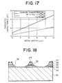
- Fig. 17 shows the relation between the width of the p-n junction portion of burying layers (hereinafter referred to as a mesa width) and the parasitic capacitance thereof.
- a mesa width the width of the p-n junction portion of burying layers
- the parasitic capacitance As denoted by a solid line in Fig. 17, to decrease the parasitic capacitance to 3 pF or lower, it is necessary to decrease the mesa width of the burying layers to 4.8 ⁇ m or lower.
- Fig. 18 shows a buried hetero semiconductor laser with a narrowed mesa width.
- the mesa width that is the width of the p-n junction portion of the burying layer is 4.8 ⁇ m
- the width of a mesa top portion MT is 3 ⁇ m. It was very difficult to form a p-side electrode and so forth on the narrow mesa top portion MT.
- the width of the electrode will become as large as around 1 ⁇ m.
- the series resistance of the wiring portion will become large.
- the time constant proportional to the product of capacitance and series resistance
- the width of the depletion layer that takes place with a bias voltage applied to the p-n junction can be increased.
- the parasitic capacitance can be reduced without the narrowed mesa width.
- a broken line shown in Fig. 17 represents the relation between the parasitic capacitance and the mesa width in the case that the carrier concentration of the n-type InP burying layer 55 is 1 x 10 17 cm -3 .
- the carrier concentration is 1 x 10 17 cm -3
- the parasitic capacitance of the junction portion is 3 pF or lower.
- the leak current increases and thereby the oscillation threshold current increases.
- the threshold current is 6 mA.
- the threshold current becomes 9 mA. In other words, the threshold current adversely increases by 50 %.
- the device parasitic capacitance may become around 1 pF.
- the optimum width of the active layer for the fundamental transverse mode oscillation is as large as around 2.5 ⁇ m, the oscillation threshold current becomes high (for example, around 11 mA).
- the active layer of the ridge waveguide semiconductor laser is a little wider than that of the buried hetero semiconductor laser, after the oscillation is started, the carrier density becomes slightly low. Thus, it is relatively difficult to increase the relaxation oscillation frequency.
- An object of the present invention is to provide an optical semiconductor device that features a low threshold current and easiness of a single transverse mode oscillation and that has a low parasitic capacitance that allows a direct modulation at high speed; and a fabricating method thereof.
- An optical semiconductor device comprises a first conduction type substrate, an active layer formed in a stripe on the first conduction type substrate, a mesa shaped burying layer formed around the active layer and having a larger band gap than that of the active layer, and a groove that electrically isolates the burying layer, wherein the section of the burying layer is in an inverse trapezoid shape of which the upper base side is longer than the lower base side.
- An optical semiconductor device comprises a first conduction type substrate, an active layer formed on the first conduction type substrate, a current confinement layer formed in a ridge stripe on the active layer, a groove that electrically isolates the current confinement layer, the groove having a space portion, and a floating wiring portion formed over the groove.
- An optical semiconductor device comprises a first conduction type substrate, an active layer formed on the first conduction type substrate, and a mesa shaped current confinement layer formed on the active layer, wherein a floating wiring portion is formed around the current confinement layer.
- a method for fabricating an optical semiconductor device comprises preparing a first conduction type substrate, forming an active layer in a stripe on the first conduction type substrate, forming a burying layer around the active layer, the burying layer having a band gap larger than that of the active layer, forming grooves that isolate the burying layer in a stripe so as to form the section of the burying layer in an inverse trapezoid shape of which the upper base side is longer than the lower base side, forming a resin layer filled in the groove, forming wiring on the resin layer, and selectively etching the resin layer so as to remove all or part of the resin layer and form a space portion in the groove below the wiring.
- a method for fabricating an optical semiconductor device comprises preparing a first conduction type substrate, forming an active layer on the first conduction type substrate, forming a current confinement layer on the active layer, forming a resin layer filled around the current confinement layer, forming wiring on the resin layer, and selectively etching the resin layer so as to remove all or part of the resin layer and form a space portion below the wiring.
- Fig. 1 is a perspective view showing a configuration of a semiconductor laser according to a first embodiment of the present invention.
- Fig. 2 is a perspective view showing a fabricating process of the semiconductor laser according to the first embodiment of the present invention.
- Fig. 3 is a perspective view showing a fabricating process of the semiconductor laser according to the first embodiment of the present invention.
- Fig. 4 is a perspective view showing a fabricating process of the semiconductor laser according to the first embodiment of the present invention.
- Fig. 5 is a perspective view showing a fabricating process of the semiconductor laser according to the first embodiment of the present invention.
- Fig. 6 is a perspective view showing a fabricating process of the semiconductor laser according to the first embodiment of the present invention.
- Fig. 7 is a perspective view showing a fabricating process of the semiconductor laser according to the first embodiment of the present invention.
- Fig. 8 is a perspective view showing a fabricating process of the semiconductor laser according to the first embodiment of the present invention.
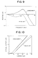
- Fig. 9 is a diagram showing a frequency characteristic of the semiconductor laser according to the first embodiment of the present invention.
- Fig. 10 is a diagram showing the comparison between I - L characteristics of the semiconductor laser according to the first embodiment and I - L characteristics of a existing semiconductor laser having a low carrier concentration.
- Fig. 11 is a diagram showing the relation between a carrier concentration of an n-type InP burying layer and a threshold current of the semiconductor laser according to the first embodiment of the present invention.
- Fig. 12A is a diagram showing a result of a reliability test in the case that the filled resin of the semiconductor laser according to the first embodiment of the present invention is benzocyclobutene resin.
- Fig. 12B is a diagram showing a result of a reliability test in the case that the filled resin of the semiconductor laser according to the embodiment of the present invention is polyimide resin.
- Fig. 13 is a perspective view showing a configuration of a semiconductor laser according to a second embodiment of the present invention.
- Fig. 14 is a sectional view showing a configuration of a semiconductor laser according to a third embodiment of the present invention.
- Fig. 15 is a sectional view showing a configuration of an optical semiconductor device according to a fourth embodiment of the present invention.
- Fig. 16 is a sectional view showing a configuration of a existing buried hetero semiconductor laser.
- Fig. 17 is a diagram showing the relation between a mesa width of burying layers and a parasitic capacitance of a existing buried hetero semiconductor laser.
- Fig. 18 is a sectional view showing a configuration of another example of a existing buried hetero semiconductor laser.
- a low device capacitance can be easily accomplished.
- an optical semiconductor device that can modulate a signal having a high frequency of 10 Gb/s or more can be accomplished.
- the sectional shape of burying layer is an inverse trapezoid of which the upper base side is longer than the lower base side, the width and area of the p-n junction portion of the burying layer can be reduced. As a result, a low device capacitance can be accomplished. Thus, in addition to a low threshold current and easiness of a single transverse mode oscillation as features of the buried hetero structure, the device parasitic capacitance can be reduced.
- the burying layer has a laminated structure of a first conduction type semiconductor layer and a second conduction type semiconductor layer.
- the carrier concentrations of the first conduction type semiconductor layer and the second conduction type semiconductor layer are larger than 1 x 10 17 cm -3 .
- the leak current can be reduced.
- the lowest layer of the burying layer is an etching stop layer.
- the lowest layer of the burying layer is composed of a constituent different from the upper layer, the lowest layer functions as a stopping layer for etching.
- the inversely trapezoidal burying layer can be effectively formed by means of wet etching.
- a resin layer is formed in the groove that electrically isolates the burying layer.
- a wiring that connects an electrode and a bonding pad can be easily formed.
- resin that composes the resin layer may be benzocyclobutene resin.
- the upper surface of the resin layer is disposed at a lower position than the upper surface of the burying layers. Thereby, a floating wiring is disposed over the groove.
- a no substance is filled in the groove.
- a floating wiring is disposed over the groove.
- the concentration of a thermal stress to the active layer can be suppressed or reduced.
- the parasitic capacitance of the wiring portion can be reduced.
- resin filled in a groove that electrically isolates a current confinement layer is selectively etched out, and all or part the resin is removed. Since a space portion is formed at a lower portion of a wiring portion disposed over the groove, a thermal stress is suppressed from being allied to the active layer. As a result, a high reliability is obtained. In addition, since the dielectric constant of the space portion is 1 (one) that is lower than that of the resin, the parasitic capacitance of the wiring portion is reduced.
- part or all of a resin layer formed around a mesa shaped current confinement layer is etched out. Accordingly, since a space portion is formed at a lower portion of a wiring portion, a thermal stress is suppressed from being applied to the active layer. As a result, a high reliability is obtained. In addition, the parasitic capacitance of the wiring portion is reduced.
- Fig. 1 is a perspective view showing a configuration of a semiconductor laser according to a first embodiment of the present invention.
- reference numeral 1 represents an n-type InP substrate.
- An n-type InP buffer layer 2 is formed on the n-type InP substrate 1.
- a mesa shaped stripe portion ST is formed on the n-type InP buffer layer 2.
- the mesa shaped stripe portion ST has a laminated structure of which an InGaAsP-MQW active layer 3, a p-type InGaASP guide layer 4, and a p-type InP layer 5 are successively formed.
- Burying layer GM is formed around the stripe portion ST.
- the burying layer GM has an inversely trapezoidal section of which the upper base side is longer than the lower base side.
- the stripe portion ST is buried in the burying layer GM.
- Grooves 6 are formed on both sides of the burying layer GM.
- the groove 6 isolates adjacent burying layers GM.
- the depth of the groove 6 is for example 6 ⁇ m.
- the burying layer GM has a p-type InP burying layer 7 and an n-type InP burying layer 8 that is disposed on the p-type InP burying layer 7.
- a p-type InP cladding layer 9 and a p-type InGaAs contact layer 10 are successively grown on the n-type InP burying layer 8.
- a stopping layer 11 for etching (a etching stop layer 11) is formed on the lowest layer of the burying layers GM.
- the etching stop layer 11 is composed of p-type InGaAsP.
- the width of the upper portion of the inverse trapezoid (namely, the width of the upper portion of the burying layer GM) is for example around 12 ⁇ m.
- the width of the lower portion (mesa neck width) is for example 4 ⁇ m.
- a SiO 2 film 12 is formed in the groove 6 that electrically isolates the burying layers GM. Resin 13 is filled in the groove 6.
- a p-side electrode 14 is formed on the p-type InGaAs contact layer 10 disposed on an upper portion of the burying layer GM.
- a bonding pad 15 is formed on the p-side electrode 14 and the resin 13 layer.
- an n-side electrode 16 is formed on the rear surface of the n-type InP substrate 1.
- the burying layer GM has an inversely trapezoidal section.
- the area of the surface of the junction of the p-type InP burying layer 7 and the n-type InP burying layer 8 that compose the burying layers GM is smaller than that of the prior art. Consequently, the parasitic capacitance caused by the junction can be reduced. As a result, the device capacitance of around 3 pF or lower can be accomplished with high reproducibility.
- the bonding pad 15 that is connected to the p-side electrode 14 can be easily formed on the resin layer 13.
- a wiring can be easily formed.
- the InGaAsP layer (the etching stop layer 11) whose etching speed is very slow in comparison with the p-type InP burying layer 7 and the n-type InP burying layer 8 is disposed on a bottom face of the groove 6, when the groove 6 is formed and the burying layer GM is formed in an inversely trapezoidal shape by means of wet etching and so on, the etching process can be automatically stopped just above the etching stop layer 11. Thus, the etching process can be easily controlled.
- the n-type InP buffer layer 2, the InGaAsP-MQW active layer 3, and the p-type InGaAsP guide layer 4 are successively epitaxially crystal-grown on the n-type InP substrate 1 whose main plane is plane orientation (100). These may be deposited by means of, for instance, MOCVD (metal-organic chemical vapor deposition), MBE (molecular beam epitaxy), ALE (atomic layer epitaxy) and so on. Thereafter, as shown in Fig. 3, a diffraction grading 17 is formed on the p-type InGaAsP guide layer 4. Next, as shown in Fig. 4, the p-type InP layer 5 is crystal-grown on the diffraction grading 17.
- MOCVD metal-organic chemical vapor deposition
- MBE molecular beam epitaxy
- ALE atomic layer epitaxy
- a SiO 2 film is deposited on the entire surface of the p-type InP layer 5 by means of CVD. Thereafter, as shown in Fig. 5, the SiO 2 film is patterned in a stripe by means of photolithography and etching. As a result, a SiO 2 film pattern 18 is formed.
- the width of the SiO 2 film pattern 18 is for example 3 ⁇ m. With the SiO 2 film pattern 18 as a mask, the wet etching process is performed. As a result, a mesa shaped stripe portion ST is formed.
- a stopping layer for etching 11 composed of p-type InGaAsP, a p-type InP burying layer 7, and an n-type InP burying layer 8 are successively formed on the n-type InP buffer layer 2 by means of MOCVD. Since crystals are not grown on the SiO 2 film, the etching stop layer 11, the p-type InP burying layer 7, and the n-type InP burying layer 8 are selectively grown on both sides of the stripe portion ST.
- the carrier concentrations of the p-type InP burying layer 7 is 1 x 10 18 cm -3 and that of the n-type InP burying layer 8 is 1 x 10 18 cm -3 .
- a p-type InP cladding layer 9 and a p-type InGaAs contact layer 10 are successively epitaxially crystal-grown on an entire surface.
- the p-type InP burying layer 7, the n-type InP burying layer 8, the p-type InP cladding layer 9, and the p-type InGaAs contact layer 10 are etched out corresponding to the groove 6 by means of wet etching.
- the burying layers around the active layer (mesa shaped stripe portion ST) are formed in such a manner that their section has an inversely trapezoidal shape.
- the groove 6 is wet etched as follows. First of all, the p-type InGaAs contact layer 10 is etched out by using a mixed solution of sulfuric acid and hydrogen peroxide solution. Thereafter, the InP burying layers are etched out with an etching solution of a mixed solution of hydrobromic acid and phosphoric acid so that the crystal plane of a side plane 19 becomes (111)A. Since the etching solution does not etch InGaAsP, the etching process stops just above the etching stop layer 11 composed of p-type InGaAsP.
- the depth of the groove 6 is for example 6 ⁇ m
- the width of the upper portion of the inverse trapezoid of the burying layer GM is for example 12 ⁇ m
- the width of the lower portion is 4 ⁇ m
- a SiO 2 film 12 is deposited on the entire surface by means of CVD.
- resin 13 is filled in the groove 6.
- the resin 13 is heated at a temperature in the range from 250 to 350°C and cured (cross linked).
- a p-side electrode 14 and a bonding pad 15 are formed at the top portion of the burying layer GM by means of evaporation, for example.
- the rear surface of the n-type InP substrate (wafer) 1 is ground to the thickness of 100 ⁇ m.
- An n-side electrode 16 is formed on the ground rear surface of the n-type InP substrate 1.
- n-side electrode 16 and the p-side electrode 14 are sintered so that they are alloyed. Finally, a device having a size of 300 ⁇ m long and 300 ⁇ m wide is sliced from the wafer. As a result, a semiconductor laser device is obtained.
- a crystal is grown using the MOCVD method.
- MOCVD Metal Organic Chemical Vapor Deposition
- MBE Molecular Beam Epitaxial growing
- ALE Automatic Layer Epitaxial
- the capacitance of the semiconductor laser device fabricated in the forgoing manner is 2 pF.
- the frequency characteristic of the device is as denoted by a solid line of Fig. 9.
- the frequency characteristic of the existing buried hetero semiconductor laser is denoted by a dotted line of Fig. 9.
- the device capacitance of the existing buried hetero semiconductor laser is around 6 pF that is not sufficiently low.
- the existing buried hetero semiconductor laser has a large roll-off phenomenon.
- the -3 dB cut-off frequency of the existing buried hetero semiconductor laser is 4 GHz.
- the device capacitance of the semiconductor laser according to the first embodiment is as low as 2 pF and does not have such a roll-off phenomenon.
- the -3 dB cut-off frequency of the semiconductor laser according to the first embodiment was as high as 15 GHz.
- the semiconductor laser according to the first embodiment has a sufficient characteristic as a light source for a direct modulation at 10 Gb/s.
- the device capacitance can be reduced without need to decrease the carrier concentrations of the burying layers.
- the carrier concentrations of the burying layers are 1 x 10 18 cm -3 , unlike with the case that the carrier concentrations are low, the threshold current does not be increased.
- the linearity of current - optical output (I - L) characteristic does not deteriorate.
- Fig. 10 is a diagram showing the I - L characteristic of the semiconductor laser according to the first embodiment of the present invention and the I - L characteristic of the existing semiconductor laser with low carrier concentrations (1 x 10 17 cm -3 ).
- dotted lines are straight lines that represent linearity.
- the threshold current of the semiconductor laser according to the first embodiment of the present invention is 6 mA.
- the threshold current can be remarkably reduced in comparison with that of the existing semiconductor laser whose carrier concentration is low (9 mA).
- the I - L characteristic of the semiconductor laser according to the first embodiment almost represents a straight line.
- the I - L characteristic of the existing buried hetero semiconductor laser whose carrier concentration is low largely deviates from the straight line.
- the linearity of the I - L characteristic can be improved.
- Fig. 11 is a diagram showing the relation between a carrier concentration of an n-type InP burying layer and a threshold current.
- the carrier concentrations of the burying layers can be increased to 1 x 10 18 cm -3 , a low threshold current can be easily accomplished.
- Fig. 12 is a diagram showing results of reliability tests of which benzocyclobutene resin and polyimide resin were used as resin filled in the groves of the semiconductor laser according to the first embodiment of the present invention. The tests are performed in the same condition of which the ambient temperature was 100°C and the current value was constant with 200 mA.
- the threshold current of the device was increased by 25 % or more.
- Fig. 13 is a sectional view showing a configuration of a semiconductor laser according to a second embodiment of the present invention.
- the semiconductor laser according to the second embodiment there is no resin layer in a groove 6 that electrically isolates burying layer GM and a space portion is formed in the groove 6.
- Wiring such as bonding pad 15 has a floating structure over the groove 6. Since the other portions of the semiconductor laser according to the second embodiment are the same as those of the first embodiment, their description will be omitted.
- a floating wiring portion is formed as follows.
- resin is filled in the groove 6.
- the resin is heated at a temperature in the rang from 250 to 350°C and cured.
- a p-side electrode 14 is formed at the top portion of the burying layers GM that have an inverse trapezoidal shape by means of evaporation, for example.
- a bonding pad 15 is formed on the p-side electrode 14 and the resin layer.
- all the resin filled in the groove 6 is removed by means of dry etching. For example, when the resin is etched with a mixed gas of CF 4 and O 2 , only the resin filled in the groove 6 can be selectively removed.
- the rear surface of the n-type InP substrate (wafer) 1 is ground.
- An n-side electrode 16 is formed on the ground rear surface of the n-type InP substrate 1.
- the n-side electrode 16 and the p-side electrode 14 are sintered so that they are alloyed.
- the sintering process is performed.
- a thermal stress is suppressed from being applied to the active layer 3.
- a high reliability is obtained.
- the heating temperature of the sintering process is normally higher than the curing temperature of the resin.
- the concentration of the stress to the active layer can be alleviated. Accordingly, the reliability is improved.
- wiring such as bonding pad 15 is formed over the groove 6.
- a space portion is formed below the wiring.
- the dielectric constant of the space portion is 1 that is lower than that of the resin. Consequently, the parasitic capacitance of the wiring portion can be reduced.
- the concentration of the stress to the active layer 3 can be suppressed or reduced and the parasitic capacitance of the wiring portion can be reduced.
- the floating structure of the wiring portion may be applied to the ridge waveguide semiconductor laser.
- Fig. 14 is a sectional view showing a configuration of a ridge waveguide semiconductor laser according to a third embodiment of the present invention.
- an n-type InGaAsP cladding layer 21, a InGaAsP-MQW active layer 22, and a p-type InGaAsP cladding layer 23 are successively formed on an n-type InP substrate 20.
- a ridge-stripe shaped p-type InP cladding layer 24 is formed on the p-type InGaAsP cladding layer 23.
- a p-type InGaAs contact layer 25 is formed on the ridge-stripe shaped p-type InP cladding layer 24.
- Grooves 26 that electrically isolate ridge portions RG are formed on both sides of the ridge portion RG of the p-type InP cladding layer 24.
- the ridge portion RG of the p-type InP cladding layer 24 functions as an current confinement layer.
- the ridge portion RG confines a current injected and supplied from a p-side electrode (that will be described later) and causes the current to flow in the active layer 22.
- the width of the stripe shaped portion adjacent to the active layer 22 is 2.5 ⁇ m.
- an SiO 2 film 27 is formed in the groove 26.
- a p-side electrode 28 is formed on a p-type InGaAs contact layer 25 and a wiring portion 29 such as bonding pad connected to the p-side electrode 28 is formed over the groove 26. Resin is not filled in the groove 26 and a space portion is formed therein. The wiring portion 29 such as bonding pad is formed in a floating structure.
- an n-side electrode 30 is formed on the rear surface of the n-type InP substrate 20.
- the wiring portion in the floating structure according to the third embodiment is formed in the same manner as the second embodiment.
- the p-type InP cladding layer 24 and the p-type InGaAs contact layer 25 corresponding to the groove 26 are etched out.
- the SiO 2 film 27 is deposited on the entire surface by means of CVD.
- resin is filled in the groove 26.
- the resin is heated at a temperature in the range from 250 to 350°C and cured.
- the p-side electrode 28 is formed on the p-type InGaAs contact layer 25 of the ridge portion RG by means of evaporation, for example.
- the wiring portion 29 such as bonding pad is formed on the p-side electrode 28 and the resin layer in the groove 26.
- the resin filled in the groove 26 is removed by means of dry etching.
- the rear surface of the n-type InP substrate (wafer) 20 is ground and the n-side electrode 30 is formed on the rear surface of the ground rear surface of the n-type InP substrate 20.
- the n-side electrode 30 and the p-side electrode 28 are sintered so that they are alloyed.
- the sintering process is performed after all the resin filled in the groove 26 is etched out. Since the thermal stress is suppressed from being applied to the active layer 22, a high reliability is obtained.
- the wiring portion 29 such as bonding pad is formed over the groove 26 and a space portion whose dielectric constant is lower than that of the resin is formed below the wiring portion 29. Accordingly, the parasitic capacitance of the wiring portion 29 is reduced.
- a current confinement layer that confines a current injected and supplied from a p-side electrode 28 and causes the current to flow in an active layer 22 is formed in a mesa shape.
- a wiring portion 29 having a floating structure is formed around the mesa shaped current confinement layer M.
- the floating wiring structure according to the fourth embodiment can be formed in the same manner as the second and third embodiments.
- a p-type InP cladding layer 24 and a p-type InGaAs contact layer 25 are etched out so that the mesa shaped current confinement layer M is formed.
- a SiO 2 film 27 is deposited on the entire surface by means of CVD and resin 31 is filled in a lower portion around the mesa shaped current confinement layer M. Thereafter, the resin 31 is heated and cured.
- a p-side electrode 28 is formed. After a wiring portion 29 such as bonding pad is formed on the p-side electrode 28 and the resin layer 31 and with the bonding pad as a mask, the resin 31 is removed by means of dry etching. Thus, the resin 31 resides only below the bonding pad. As a result, the wiring portion 29 in the floating structure is formed. Thereafter, the rear surface of the n-type InP substrate (wafer) 20 is ground. After an n-side electrode 30 is formed on the ground rear surface of the n-type InP substrate 20 and the n-side electrode 30 and the p-side electrode 28 are sintered so that they are alloyed.
- the concentration of the thermal stress to the active layer 22 can be suppressed or reduced.
- the parasitic capacitance of the wiring portion 29 is reduced.
- the present invention is not limited to a semiconductor laser. Instead, the present invention can be applied to various types of optical semiconductor devices such as LED (Light Emitting Diode), PD (Photo Diode), optical modulator, and optical semiconductor switch.
- LED Light Emitting Diode
- PD Photo Diode
- optical modulator optical modulator
- optical semiconductor switch optical semiconductor switch
Landscapes
- Physics & Mathematics (AREA)
- Geometry (AREA)
- Condensed Matter Physics & Semiconductors (AREA)
- General Physics & Mathematics (AREA)
- Electromagnetism (AREA)
- Optics & Photonics (AREA)
- Semiconductor Lasers (AREA)
Applications Claiming Priority (4)
| Application Number | Priority Date | Filing Date | Title |
|---|---|---|---|
| JP2001097598 | 2001-03-29 | ||
| JP2001097598 | 2001-03-29 | ||
| JP2002072979A JP2002359437A (ja) | 2001-03-29 | 2002-03-15 | 光半導体素子および光半導体素子の製造方法 |
| JP2002072979 | 2002-03-15 |
Publications (2)
| Publication Number | Publication Date |
|---|---|
| EP1246329A2 true EP1246329A2 (de) | 2002-10-02 |
| EP1246329A3 EP1246329A3 (de) | 2004-12-22 |
Family
ID=26612639
Family Applications (1)
| Application Number | Title | Priority Date | Filing Date |
|---|---|---|---|
| EP02006681A Withdrawn EP1246329A3 (de) | 2001-03-29 | 2002-03-26 | Optische Halbleitervorrichtung und Herstellungsverfahren |
Country Status (3)
| Country | Link |
|---|---|
| US (1) | US6724068B2 (de) |
| EP (1) | EP1246329A3 (de) |
| JP (1) | JP2002359437A (de) |
Cited By (1)
| Publication number | Priority date | Publication date | Assignee | Title |
|---|---|---|---|---|
| EP4080698A1 (de) * | 2021-04-22 | 2022-10-26 | Nokia Solutions and Networks Oy | Doppelkanaliger versenkter wellenleiter und verfahren zur herstellung davon |
Families Citing this family (20)
| Publication number | Priority date | Publication date | Assignee | Title |
|---|---|---|---|---|
| DE10039433B4 (de) * | 2000-08-11 | 2017-10-26 | Osram Opto Semiconductors Gmbh | Halbleiterchip für die Optoelektronik |
| JP2003046197A (ja) * | 2001-08-01 | 2003-02-14 | Matsushita Electric Ind Co Ltd | 半導体レーザおよびその製造方法 |
| JP4046586B2 (ja) * | 2002-01-16 | 2008-02-13 | シャープ株式会社 | 化合物半導体素子及びその製造方法 |
| US6833556B2 (en) | 2002-08-12 | 2004-12-21 | Acorn Technologies, Inc. | Insulated gate field effect transistor having passivated schottky barriers to the channel |
| US7084423B2 (en) | 2002-08-12 | 2006-08-01 | Acorn Technologies, Inc. | Method for depinning the Fermi level of a semiconductor at an electrical junction and devices incorporating such junctions |
| JP4637097B2 (ja) * | 2004-03-29 | 2011-02-23 | 三洋電機株式会社 | 発光ダイオードアレイ、発光ダイオード及びプリンタヘッド |
| US7352006B2 (en) * | 2004-09-28 | 2008-04-01 | Goldeneye, Inc. | Light emitting diodes exhibiting both high reflectivity and high light extraction |
| US7652299B2 (en) * | 2005-02-14 | 2010-01-26 | Showa Denko K.K. | Nitride semiconductor light-emitting device and method for fabrication thereof |
| DE102006002753B4 (de) * | 2006-01-20 | 2010-09-30 | X-Fab Semiconductor Foundries Ag | Verfahren und Anordnung zur Bewertung der Unterätzung von tiefen Grabenstrukturen in SOI-Scheiben |
| JP2011014632A (ja) * | 2009-06-30 | 2011-01-20 | Sony Corp | 半導体レーザ |
| JP2011077339A (ja) * | 2009-09-30 | 2011-04-14 | Sony Corp | 半導体レーザ |
| JP5660940B2 (ja) * | 2010-04-27 | 2015-01-28 | 住友電工デバイス・イノベーション株式会社 | 光半導体装置の製造方法 |
| US9362376B2 (en) | 2011-11-23 | 2016-06-07 | Acorn Technologies, Inc. | Metal contacts to group IV semiconductors by inserting interfacial atomic monolayers |
| CN102593284B (zh) * | 2012-03-05 | 2014-06-18 | 映瑞光电科技(上海)有限公司 | 隔离深沟槽及其高压led芯片的制造方法 |
| JP6371609B2 (ja) * | 2014-07-04 | 2018-08-08 | 日本オクラロ株式会社 | 半導体発光素子 |
| JP6627651B2 (ja) * | 2016-06-09 | 2020-01-08 | 三菱電機株式会社 | レーザ素子、レーザ素子の製造方法 |
| US9620611B1 (en) | 2016-06-17 | 2017-04-11 | Acorn Technology, Inc. | MIS contact structure with metal oxide conductor |
| US10170627B2 (en) | 2016-11-18 | 2019-01-01 | Acorn Technologies, Inc. | Nanowire transistor with source and drain induced by electrical contacts with negative schottky barrier height |
| DE102018123019A1 (de) * | 2018-09-19 | 2020-03-19 | Osram Opto Semiconductors Gmbh | Gewinngeführter halbleiterlaser und herstellungsverfahren hierfür |
| WO2020183812A1 (ja) * | 2019-03-11 | 2020-09-17 | ローム株式会社 | 半導体発光装置 |
Family Cites Families (9)
| Publication number | Priority date | Publication date | Assignee | Title |
|---|---|---|---|---|
| JPS5885584A (ja) * | 1981-11-16 | 1983-05-21 | Nec Corp | 半導体レ−ザ |
| US5319661A (en) * | 1990-12-27 | 1994-06-07 | The Furukawa Electric Co., Ltd. | Semiconductor double heterostructure laser device with InP current blocking layer |
| US5360763A (en) * | 1992-09-07 | 1994-11-01 | Nec Corporation | Method for fabricating an optical semiconductor device |
| JP3007928B2 (ja) * | 1995-02-22 | 2000-02-14 | 日本電気株式会社 | 光半導体素子の製造方法 |
| JPH09199803A (ja) * | 1996-01-23 | 1997-07-31 | Mitsubishi Electric Corp | 半導体レーザおよびその製造方法 |
| JPH1075009A (ja) * | 1996-08-30 | 1998-03-17 | Nec Corp | 光半導体装置とその製造方法 |
| JPH11204879A (ja) | 1998-01-14 | 1999-07-30 | Oki Electric Ind Co Ltd | 半導体光素子及びその製造方法 |
| JP2000012963A (ja) * | 1998-06-23 | 2000-01-14 | Nec Corp | 光半導体装置の製造方法 |
| JP3225942B2 (ja) * | 1999-01-21 | 2001-11-05 | 日本電気株式会社 | 半導体光素子、その製造方法及び半導体光学装置 |
-
2002
- 2002-03-15 JP JP2002072979A patent/JP2002359437A/ja not_active Abandoned
- 2002-03-21 US US10/104,634 patent/US6724068B2/en not_active Expired - Lifetime
- 2002-03-26 EP EP02006681A patent/EP1246329A3/de not_active Withdrawn
Cited By (1)
| Publication number | Priority date | Publication date | Assignee | Title |
|---|---|---|---|---|
| EP4080698A1 (de) * | 2021-04-22 | 2022-10-26 | Nokia Solutions and Networks Oy | Doppelkanaliger versenkter wellenleiter und verfahren zur herstellung davon |
Also Published As
| Publication number | Publication date |
|---|---|
| JP2002359437A (ja) | 2002-12-13 |
| US6724068B2 (en) | 2004-04-20 |
| EP1246329A3 (de) | 2004-12-22 |
| US20020139989A1 (en) | 2002-10-03 |
Similar Documents
| Publication | Publication Date | Title |
|---|---|---|
| US6724068B2 (en) | Optical semiconductor device and fabricating method thereof | |
| KR102171268B1 (ko) | 하이브리드 실리콘 레이저 제조 방법 | |
| US6256331B1 (en) | Semiconductor laser device, optical communication system using the same, and method for producing compound semiconductor | |
| US8063408B2 (en) | Integrated semiconductor optical device and optical apparatus using the same | |
| JP3234086B2 (ja) | 光半導体デバイス及びその製造方法 | |
| CA1151275A (en) | Semiconductor laser device and method of manufacturing the same | |
| US5636237A (en) | Semiconductor laser device which makes it possible to realize high-speed modulation | |
| US5084893A (en) | Semiconductor light-emitting device | |
| US6995454B2 (en) | Semiconductor optical integrated device having a light emitting portion, a modulation section and a separation portion | |
| US6931041B2 (en) | Integrated semiconductor laser device and method of manufacture thereof | |
| US5335241A (en) | Buried stripe type semiconductor laser device | |
| US20050185689A1 (en) | Optoelectronic device having a Discrete Bragg Reflector and an electro-absorption modulator | |
| US6639926B1 (en) | Semiconductor light-emitting device | |
| US6865204B2 (en) | Ridge waveguide type photo semiconductor device and method for fabricating same | |
| US5881086A (en) | Optical semiconductor device with quantum wires, fabrication method thereof, and light source apparatus, and optical communication system using the same | |
| US5084410A (en) | Method of manufacturing semiconductor devices | |
| US5222091A (en) | Structure for indium phosphide/indium gallium arsenide phosphide buried heterostructure semiconductor | |
| CA2033246C (en) | Optical semiconductor device | |
| US7271422B2 (en) | Semiconductor optical device | |
| US5182228A (en) | Method of manufacturing a semiconductor light-emitting device | |
| Armistead et al. | Low-threshold ridge waveguide lasers at λ= 1.5 μm | |
| US20030062517A1 (en) | Semiconductor device with current confinement structure | |
| JPH05299764A (ja) | 半導体レーザの製造方法 | |
| JP4163321B2 (ja) | 半導体発光装置 | |
| JP2550729B2 (ja) | 半導体レーザ |
Legal Events
| Date | Code | Title | Description |
|---|---|---|---|
| PUAI | Public reference made under article 153(3) epc to a published international application that has entered the european phase |
Free format text: ORIGINAL CODE: 0009012 |
|
| 17P | Request for examination filed |
Effective date: 20020326 |
|
| AK | Designated contracting states |
Kind code of ref document: A2 Designated state(s): AT BE CH CY DE DK ES FI FR GB GR IE IT LI LU MC NL PT SE TR |
|
| AX | Request for extension of the european patent |
Free format text: AL;LT;LV;MK;RO;SI |
|
| PUAL | Search report despatched |
Free format text: ORIGINAL CODE: 0009013 |
|
| PUAF | Information related to the publication of a search report (a3 document) modified or deleted |
Free format text: ORIGINAL CODE: 0009199SEPU |
|
| AK | Designated contracting states |
Kind code of ref document: A3 Designated state(s): AT BE CH CY DE DK ES FI FR GB GR IE IT LI LU MC NL PT SE TR |
|
| AX | Request for extension of the european patent |
Extension state: AL LT LV MK RO SI |
|
| D17D | Deferred search report published (deleted) | ||
| PUAL | Search report despatched |
Free format text: ORIGINAL CODE: 0009013 |
|
| AK | Designated contracting states |
Kind code of ref document: A3 Designated state(s): AT BE CH CY DE DK ES FI FR GB GR IE IT LI LU MC NL PT SE TR |
|
| AX | Request for extension of the european patent |
Extension state: AL LT LV MK RO SI |
|
| AKX | Designation fees paid |
Designated state(s): DE FR GB |
|
| STAA | Information on the status of an ep patent application or granted ep patent |
Free format text: STATUS: THE APPLICATION IS DEEMED TO BE WITHDRAWN |
|
| 18D | Application deemed to be withdrawn |
Effective date: 20050601 |