EP1242836B1 - CALCIUM FLUORIDE (CaF2) STRESS PLATE AND METHOD OF MAKING THE SAME - Google Patents
CALCIUM FLUORIDE (CaF2) STRESS PLATE AND METHOD OF MAKING THE SAME Download PDFInfo
- Publication number
- EP1242836B1 EP1242836B1 EP00988198A EP00988198A EP1242836B1 EP 1242836 B1 EP1242836 B1 EP 1242836B1 EP 00988198 A EP00988198 A EP 00988198A EP 00988198 A EP00988198 A EP 00988198A EP 1242836 B1 EP1242836 B1 EP 1242836B1
- Authority
- EP
- European Patent Office
- Prior art keywords
- caf
- plate
- transmission axis
- planes
- force
- Prior art date
- Legal status (The legal status is an assumption and is not a legal conclusion. Google has not performed a legal analysis and makes no representation as to the accuracy of the status listed.)
- Expired - Lifetime
Links
Images


Classifications
-
- G—PHYSICS
- G02—OPTICS
- G02B—OPTICAL ELEMENTS, SYSTEMS OR APPARATUS
- G02B5/00—Optical elements other than lenses
- G02B5/30—Polarising elements
-
- G—PHYSICS
- G03—PHOTOGRAPHY; CINEMATOGRAPHY; ANALOGOUS TECHNIQUES USING WAVES OTHER THAN OPTICAL WAVES; ELECTROGRAPHY; HOLOGRAPHY
- G03F—PHOTOMECHANICAL PRODUCTION OF TEXTURED OR PATTERNED SURFACES, e.g. FOR PRINTING, FOR PROCESSING OF SEMICONDUCTOR DEVICES; MATERIALS THEREFOR; ORIGINALS THEREFOR; APPARATUS SPECIALLY ADAPTED THEREFOR
- G03F7/00—Photomechanical, e.g. photolithographic, production of textured or patterned surfaces, e.g. printing surfaces; Materials therefor, e.g. comprising photoresists; Apparatus specially adapted therefor
- G03F7/70—Microphotolithographic exposure; Apparatus therefor
- G03F7/708—Construction of apparatus, e.g. environment aspects, hygiene aspects or materials
- G03F7/7095—Materials, e.g. materials for housing, stage or other support having particular properties, e.g. weight, strength, conductivity, thermal expansion coefficient
- G03F7/70958—Optical materials or coatings, e.g. with particular transmittance, reflectance or anti-reflection properties
- G03F7/70966—Birefringence
-
- C—CHEMISTRY; METALLURGY
- C30—CRYSTAL GROWTH
- C30B—SINGLE-CRYSTAL GROWTH; UNIDIRECTIONAL SOLIDIFICATION OF EUTECTIC MATERIAL OR UNIDIRECTIONAL DEMIXING OF EUTECTOID MATERIAL; REFINING BY ZONE-MELTING OF MATERIAL; PRODUCTION OF A HOMOGENEOUS POLYCRYSTALLINE MATERIAL WITH DEFINED STRUCTURE; SINGLE CRYSTALS OR HOMOGENEOUS POLYCRYSTALLINE MATERIAL WITH DEFINED STRUCTURE; AFTER-TREATMENT OF SINGLE CRYSTALS OR A HOMOGENEOUS POLYCRYSTALLINE MATERIAL WITH DEFINED STRUCTURE; APPARATUS THEREFOR
- C30B29/00—Single crystals or homogeneous polycrystalline material with defined structure characterised by the material or by their shape
- C30B29/10—Inorganic compounds or compositions
- C30B29/12—Halides
-
- C—CHEMISTRY; METALLURGY
- C30—CRYSTAL GROWTH
- C30B—SINGLE-CRYSTAL GROWTH; UNIDIRECTIONAL SOLIDIFICATION OF EUTECTIC MATERIAL OR UNIDIRECTIONAL DEMIXING OF EUTECTOID MATERIAL; REFINING BY ZONE-MELTING OF MATERIAL; PRODUCTION OF A HOMOGENEOUS POLYCRYSTALLINE MATERIAL WITH DEFINED STRUCTURE; SINGLE CRYSTALS OR HOMOGENEOUS POLYCRYSTALLINE MATERIAL WITH DEFINED STRUCTURE; AFTER-TREATMENT OF SINGLE CRYSTALS OR A HOMOGENEOUS POLYCRYSTALLINE MATERIAL WITH DEFINED STRUCTURE; APPARATUS THEREFOR
- C30B33/00—After-treatment of single crystals or homogeneous polycrystalline material with defined structure
-
- G—PHYSICS
- G02—OPTICS
- G02B—OPTICAL ELEMENTS, SYSTEMS OR APPARATUS
- G02B1/00—Optical elements characterised by the material of which they are made; Optical coatings for optical elements
- G02B1/02—Optical elements characterised by the material of which they are made; Optical coatings for optical elements made of crystals, e.g. rock-salt, semi-conductors
-
- G—PHYSICS
- G02—OPTICS
- G02B—OPTICAL ELEMENTS, SYSTEMS OR APPARATUS
- G02B5/00—Optical elements other than lenses
- G02B5/30—Polarising elements
- G02B5/3083—Birefringent or phase retarding elements
-
- G—PHYSICS
- G02—OPTICS
- G02F—OPTICAL DEVICES OR ARRANGEMENTS FOR THE CONTROL OF LIGHT BY MODIFICATION OF THE OPTICAL PROPERTIES OF THE MEDIA OF THE ELEMENTS INVOLVED THEREIN; NON-LINEAR OPTICS; FREQUENCY-CHANGING OF LIGHT; OPTICAL LOGIC ELEMENTS; OPTICAL ANALOGUE/DIGITAL CONVERTERS
- G02F1/00—Devices or arrangements for the control of the intensity, colour, phase, polarisation or direction of light arriving from an independent light source, e.g. switching, gating or modulating; Non-linear optics
- G02F1/01—Devices or arrangements for the control of the intensity, colour, phase, polarisation or direction of light arriving from an independent light source, e.g. switching, gating or modulating; Non-linear optics for the control of the intensity, phase, polarisation or colour
- G02F1/0128—Devices or arrangements for the control of the intensity, colour, phase, polarisation or direction of light arriving from an independent light source, e.g. switching, gating or modulating; Non-linear optics for the control of the intensity, phase, polarisation or colour based on electro-mechanical, magneto-mechanical, elasto-optic effects
- G02F1/0131—Devices or arrangements for the control of the intensity, colour, phase, polarisation or direction of light arriving from an independent light source, e.g. switching, gating or modulating; Non-linear optics for the control of the intensity, phase, polarisation or colour based on electro-mechanical, magneto-mechanical, elasto-optic effects based on photo-elastic effects, e.g. mechanically induced birefringence
-
- G—PHYSICS
- G02—OPTICS
- G02F—OPTICAL DEVICES OR ARRANGEMENTS FOR THE CONTROL OF LIGHT BY MODIFICATION OF THE OPTICAL PROPERTIES OF THE MEDIA OF THE ELEMENTS INVOLVED THEREIN; NON-LINEAR OPTICS; FREQUENCY-CHANGING OF LIGHT; OPTICAL LOGIC ELEMENTS; OPTICAL ANALOGUE/DIGITAL CONVERTERS
- G02F1/00—Devices or arrangements for the control of the intensity, colour, phase, polarisation or direction of light arriving from an independent light source, e.g. switching, gating or modulating; Non-linear optics
- G02F1/01—Devices or arrangements for the control of the intensity, colour, phase, polarisation or direction of light arriving from an independent light source, e.g. switching, gating or modulating; Non-linear optics for the control of the intensity, phase, polarisation or colour
- G02F1/0136—Devices or arrangements for the control of the intensity, colour, phase, polarisation or direction of light arriving from an independent light source, e.g. switching, gating or modulating; Non-linear optics for the control of the intensity, phase, polarisation or colour for the control of polarisation, e.g. state of polarisation [SOP] control, polarisation scrambling, TE-TM mode conversion or separation
Definitions
- the present invention is generally related to optical stress plates that are used for delaying optical wavefronts, and methods for making the same.
- Many semiconductor fabrication systems utilizes photolithography techniques in the fabrication of semiconductor wafers.
- one or more layers of circuit patterns are built up on a semiconductor wafer. This is accomplished by illuminating a reticle with light, where the reticle contains a desired circuit pattern. The resulting reticle image is then projected onto photosensitive resist that covers the semiconductor wafer. After a series of exposures and subsequent processing, a semiconductor wafer containing the desired circuit pattern is manufactured.
- circuit features of 0.25 ⁇ m have been achieved with photolithography systems using light wavelengths of 193 nm (nanometers). To achieve geometries below 0.25 ⁇ m, even smaller wavelengths (e.g.157 nm) must be used.
- the illumination system used in photolithography includes various optical components that manipulate light to project a reticle image on the semiconductor wafer.
- One common component in the illumination system is an optical delay plate (also called a stress plate). Stress plates can be used to delay or retard a light wavefront by a specified amount. Stress plates can also be used to convert the polarization of light from one polarization to another. For example, a 1 ⁇ 4 (quarter) wave stress plate that is rotated 45 degrees to the incident light converts linearly polarized light to circularly polarized light and visa-versa. In another example, horizontally polarized light is converted to vertically polarized light by using a 1 ⁇ 4 wave stress plate and a mirror.
- a stress plate In order for a stress plate to function as desired, it must be fabricated from a material that will transmit sufficient light at the wavelength of interest.
- Conventional stress plates are made of fused silica or man-made quartz. These conventional materials do not sufficiently transmit light at wavelengths that are below 193 nm.
- the smallest feature that can be fabricated on the semiconductor wafer is limited to the optical wavelength of the light used in the system.
- photolithography systems that utilize conventional stress plates can manufacture features that are no smaller than approximately 0.25 ⁇ m. Therefore, what is needed is a stress plate that is functional at optical wavelengths that are below 193 nm (including 157 nm) to support the fabrication of semiconductor wafers having circuit features that are smaller than 0.25 ⁇ m.
- US 3600611 discloses a stress plate comprising CaF 2 .
- the present invention is directed at a Calcium Fluoride (CaF 2 ) optical stress plate and a method for making the same as defined in the appended claims.
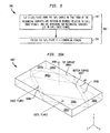
- FIG. 1 illustrates an example environment including illumination system 100 for focusing light on a wafer 127.
- Illumination system 100 can be part of a photolithography system for manufacturing a desired circuit pattern on the wafer 127.
- Illumination system 100 includes: a light source 103; a mirror 106; a stress plate 109; a beam splitter cube 121 having sections 112 and 118 and coating(s) 115; and a focus module 124.
- Illumination system 100 operates as follows.
- Light source 103 provides a light wavefront 104 having a specific wavelength and polarization that is incident on the beam splitter cube 121.
- the light wavefront 104 is vertically polarized, although other polarizations could be used.
- the light wavefront 104 passes through section 112 of the cube 121 and is incident on the coating 115.
- the coating 115 has optical transmission properties that vary depending on the polarization of the incident light. When the incident light is vertically polarized, the coating 115 is reflective. When incident light is horizontally polarized, then the coating 115 is transmissive. Since wavefront 104 is vertically polarized, it is reflected upward by the coating 115 to the stress plate 109.
- Stress plate 109 is approximately a 1 ⁇ 4 wave stress plate at the wavelength of interest and is rotated by 45 degrees in the zx plane relative to the incident wavefront. The result is that the stress plate 109 converts the vertically polarized light to circularly polarized (CP) light 107, which is incident on the mirror 106.
- CP circularly polarized
- the mirror 106 reflects the CP light 107 and reverses the circular polarization to generate reversed CP light 108.
- the CP light 108 propagates back through the stress plate 109 and is converted to horizontally polarized light 110 that is incident on the cube 121. Therefore, by passing linearly polarized light though a 1 ⁇ 4 wave stress plate twice using a mirror, the linear polarization is maintained but the polarization is rotated by 90 degrees.
- the cube 121 passes the horizontally polarized light 110 to the focus module 124 without substantial change. This occurs because the coating 115 is transmissive to horizontally polarized light as discussed above.
- the focus module 124 contains the reticle having the desired circuit pattern.
- the focus module 124 causes the incident light to pass through the reticle generating a reticle image 126 that is focused on the wafer 127.
- FIG. 2A illustrates stress plate 200 for delaying an optical wavefront according to embodiments of the present invention.
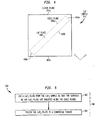
- Stress plate 200 is made of calcium fluoride material having the chemical symbol CaF 2 .
- CaF 2 has a well known crystalline structure that is face centered cubic.
- FIG. 2B illustrates the face centered cubic structure for CaF 2 , and includes 8 calcium (Ca) ions that define a cube having an additional Ca ion in the center of each of the six surfaces of the cube. (The fluorine ions are not shown for ease of illustration.)
- the outer surfaces of the cube are the cubic planes, and the cleave planes are defined by the dotted lines.
- a portion of a cleave plane is defined by Ca ions Ca 1 , Ca 2 , and Ca 3 , is cross-hatched. The easiest plane to cut or break a crystal material is along the cleave planes, and not the cubic planes.
- An advantage of making an optical delay out of CaF 2 is that CaF 2 is able to transmit electromagnetic waves having wavelengths that are below 193 nm (including wavelengths at 157 nm) with relatively little attenuation when compared to traditional optical materials such as fused silica or man-made quartz. Therefore, CaF 2 stress plates enable manufacturing processes to fabricate semiconductors with circuit geometries that are smaller than 0.25 ⁇ m.
- the stress plate 200 has two different indexes of refraction that are seen by electromagnetic (EM) fields depending on the EM field orientation.
- the first index of refraction is n 1 and is seen by EM fields that are oriented with vector 203.
- the second index of refraction is n 2 and is seen by an EM fields that are oriented with vector 206.
- the index of refraction for a material defines the phase velocity for an electromagnetic wave traveling through the material relative to the phase velocity in free space.
- n 1 is the characteristic index of refraction for undisturbed CaF 2
- n 2 is a higher or lower index of refraction caused by a compression or tensile force that is aligned with the vector 206.
- the modification of the characteristic index of refraction for CaF 2 using compression and/or tensile forces is discussed further in the following section.
- both n 1 and n 2 are different from the index of refraction for undisturbed CaF 2 , where one (n 1 or n 2 ) has a higher index of refraction than undisturbed CaF 2 , and the other one has a lower index of refraction than undisturbed CaF 2 .
- vector 203 is referred to as the index of refraction vector 203 and is assumed to include its associated index of refraction n 1 .
- vector 206 is referred to as the index of refraction vector 206 and is assumed to include the associated index of refraction n 2 .
- both index of refraction vectors 203 and 206 are perpendicular to an associated set of CaF 2 cubic planes, and therefore are perpendicular to each other.
- the vectors 203 and 206 are also perpendicular to a transmission axis 209 that is associated with the stress plate 200.
- the transmission axis 209 defines the direction that an optical wavefront is required to travel through the stress plate 200 in order to achieve the desired delay.
- the first index of refraction vector 203 is aligned along the z-axis
- the second index refraction vector 206 is aligned in the x-axis, as defined by the coordinate system for FIG. 2A.
- the transmission axis 209 is along the y-axis through the plate 200.
- the desired optical delay can be achieved by transmitting the optical wavefront 212 through either side of the stress plate 200 along the y-axis.
- the optical wavefront 212 When an optical wavefront 212 passes through the stress plate along the transmission axis 209, the optical wavefront is retarded or delayed by an amount that is proportional to the differences between the index of refraction vectors.
- the delay occurs because the optical wavefront 212 has an EM field component that is oriented with the first index of refraction vector 203, and an EM field component that is oriented with the second index of refraction vector 206.
- the field component oriented with the vector 203 will have a different phase velocity than that of the field component oriented with the vector 206 while passing through the stress plate 200, and thereby implementing the delay.
- a CaF 2 stress plate operates to delay an optical wavefront by having two different indexes of refraction that are seen by different field components of the optical wavefront.
- the present section describes methods of fabricating a CaF 2 stress plate using compressive, tensile, and shear forces that are applied to cubic plane surfaces of the CaF 2 plate.
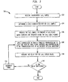
- FIG. 3 depicts operational flowchart 300 that describes a method of producing a CaF 2 stress plate from a sample of CaF 2 material according to embodiments ofthe invention.
- Flowchart 300 is described as follows.
- FIG. 4 illustrates a CaF 2 sample 402 having cleave planes 404 and cubic planes 406. Unprocessed samples are typically oriented in a cleave plane because the cleave plane is the most convenient plane to cut the sample from a newly grown CaF 2 ingot.
- a step 304 the orientation of the cubic planes for the CaF 2 sample are determined. Determining the cubic plane orientation for a sample can be done using known x-ray techniques or other standard techniques. The cubic plane orientation is determined so that a CaF 2 plate having surfaces oriented along the cubic planes can be cut from the CaF 2 sample, as illustrated by CaF 2 plate 408 that is defined by cubic planes 406 in FIG. 4.
- a step 306 the CaF 2 sample is processed to generate a CaF 2 plate having all 6 surfaces that lie in CaF 2 cubic planes.
- Step 306 is further described by flowchart 500 that is shown in FIG. 5 and is described as follows.
- a CaF 2 plate that is oriented in the CaF 2 cubic planes is cut from the CaF 2 sample, as illustrated by CaF 2 plate 408 that is shown in FIG. 4.
- the CaF 2 plate is polished to a commercial finish, so that the surfaces are sufficiently flat and parallel for optical transmission.
- FIG. 6A depicts the CaF 2 plate 408 after being cut from the sample 402, where all 6 surfaces 406a-f of the plate lie in a CaF 2 cubic plane.
- a compression force or tensile force is applied perpendicular to at least one set of cubic plane surfaces and perpendicular to the transmission axis for an incident optical wavefront.
- the compression or tensile force stresses the plate in the direction of the force, which changes the index of refraction for electromagnetic fields that are oriented along the direction of the stress.
- the stressed CaF 2 plate effectively has two indices of refraction.
- One index of refraction is seen by electromagnetic fields that are oriented in the direction of the stress.
- the other index of refraction is seen by electromagnetic fields that are oriented in non-stress directions. It is the different refraction indexes according to field orientation that cause the desired delay for the optical wavefront traveling along the transmission axis.
- FIGs. 6B-6G illustrate the various embodiments for the application of compression and/or tensile forces in the step 308 to the CaF 2 plate 408.
- These figures include an optical wavefront 602 that is incident on the surface 406b along the y-axis to define the transmission axis relative to the applied force vectors. (Surface 406b is illustrated as the bottom surface for simplicity.)
- the optical wavefront 602 should be incident perpendicular to the surface 406b (and therefore perpendicular to the force vectors). The same delay is achieved if the optical wavefront is incident on the top surface 406a.
- the optical wavefront 602 is a traverse electromagnetic (TEM) wave
- the wavefront 602 will have an EM field component in the x-direction and an EM field component in the z-direction, as will be understood by those skilled in the arts.
- FIGs. 6B-6D are now discussed in more detail.
- the compression force 604a and 604b is applied along the x-direction and perpendicular to surfaces 406c and 406d of the CaF 2 plate 408.
- compression force can be applied using one or more screws that are abutted to the surfaces 406c,d.
- the compressive force should be applied uniformly along the surfaces 406c and 406d using multiple screws.
- the compression force will cause an internal stress that changes the index of refraction for the CaF 2 plate that is seen by EM fields that are oriented in the x-direction.
- the index of refraction for EM fields that are oriented in the z-direction remains unchanged.
- the optical wavefront 602 will be delayed by traveling through the plate 408 because the EM fields that are oriented in x-direction are delayed compared to those EM fields that are oriented in the z direction.
- Experimental results show that 90 degrees of delay can be achieved at the 157 nm wavelength by applying 300-500 psi of force.
- a tensile force (or pulling force) 606a,b is applied perpendicular to surfaces 406c and 406d.
- tensile force can be applied by epoxying a bar to each surface 406c and 406d and pulling outward on the bars. As described above, the applied force changes the index of refraction for EM fields that are oriented in the force direction, thereby causing the desired delay.
- a compression force 608a,b is applied to surfaces 406e and 406f.
- the applied force 608 changes the index of refraction for EM fields that are oriented in the z direction but not the x-direction, thereby causing the desired delay.
- a tensile force (or pulling force) 610a,b is applied perpendicular to the surfaces 406e and 406f to implement the desired delay.
- a compression force 612a,b is applied perpendicular to surfaces 406c and 406d
- a tensile force 614a,b is applied perpendicular to surfaces 406e and 406f.
- the index of refraction for EM fields oriented in the x direction is changed, as well as the index of refraction for EM fields that are oriented in the z direction.
- one index of refraction is increased and the other is decreased because one force is a compression force and the other force is a tensile force.
- a tensile force 614a,b is applied perpendicular to surfaces 406c and 406d and a compression force 616a,b is applied perpendicular to surfaces 406e and 406f. Similar to that described in FIG. 6F, the indexes of refraction for EM waves oriented in both the x-direction and z-direction are changed but the variations have opposite signs.
- the optical delay is measured at the wavelength of interest to determined if it is the desired amount of delay.
- various apparatus including polarimeters, for measuring optical delay that are known by those skilled in the relevant arts.
- FIG. 7 illustrates measurement system 700 for determining if the optical delay ofthe stress plate 408 has reached a desired 90 degrees for the incident optical wavefront 602.
- the optical wavefront 602 is vertically polarized.
- Fig. 7 includes a vertical polarizer 703, the stress plate 408, a mirror 706, and a detector 709, and operates as follows.
- the polarizer 703 is matched to the vertical polarized wavefront 602, and therefore substantially passes the wavefront 602 to the stress plate 408.
- the stress plate 408 is rotated by 45 degrees in zx plane, and thereby converts the wavefront 602 to a circular polarized wavefront 707.
- the mirror 706 reflects the CP wavefront 707 and reverses the CP polarization to generate CP wavefront 708.
- the CP wavefront 708 passes back through the stress plate 408 and is converted to substantially horizontally polarized light 704 if the stress plate delay is substantially 90 degrees.
- the vertical polarizer 703 receives the light 704 and rejects any content that is horizontally polarized and passes the vertical content as light 702.
- the detector 709 measures the signal strength of the light 702 that passes through the polarizer 703. The closer the delay of the stress plate 408 is to 90 degrees, the more the light 704 is rejected and the smaller the signal strength that is measured for the light 702. As the stress plate delay varies from 90 degrees, the detector 709 will detect a higher signal strength of light passing through the polarizer 703.
- a step 312 it is determined whether the delay of the stress plate is sufficiently close to the desired amount. If the measurement system 700 is used, then the decision 312 is made based the measured signal strength of the light 702. In other words, if the signal strength is above a threshold, then the delay is not sufficiently close to the desired 90 degrees. If the delay is sufficient, then the process ends and the stress plate 408 is complete and is ready for use. If the delay is not sufficient then the compression and/or tensile force can be incremented in step 314, and the measurement process can be repeated until the desired delay is reached.
- FIG. 8 depicts a flowchart 800 that describes a method of making a CaF 2 stress plate using one or more shear forces. Steps 302, 304 and 310-314 in flowchart 800 are the same as those described in flowchart 300, to which the reader is directed for further details. The new steps 802 and 804 are described as follows.
- a CaF 2 sample is processed to generate a CaF 2 plate having mechanical surfaces that are rotated 45 degrees relative to the CaF 2 cubic planes around the transmission axis.
- Step 802 is further described by flowchart 900 that is shown in FIG. 9 and is described as follows.
- a CaF 2 plate is cut from the CaF 2 sample so that four of the mechanical surfaces (that do not define the transmission axis) are rotated 45 degrees relative to the CaF 2 cubic planes that were found in step 304.
- Various techniques for cutting or grinding crystal materials are known by those skilled in the arts.
- the other two mechanical surfaces are cut to lie in CaF 2 cubic planes, and define the transmission axis for the optical wavefront.
- the CaF 2 plate is polished to a commercial finish, so that the surfaces are sufficiently flat and parallel as needed for optical transmission.
- FIG. 10A depicts a CaF 2 plate 1002 after being processed according to steps 902 and 904.
- the CaF 2 plate 1002 has mechanical surfaces 1004a-d that are rotated by 45 degrees around the transmission axis 1008 relative to the cubic planes 1006a-d.
- the cubic planes 1006a-d form a "diamond" shape within the plate 1002 as shown in FIG. 10A.
- the mechanical surfaces 1004e and 1004f are the "top" and “bottom” surfaces ofthe plate 1002, respectively, and lie in CaF cubic planes.
- the mechanical surfaces 1004e and 1004f are perpendicular to (and define) the optical transmission axis 1008.
- a step 804 shear forces are applied along the mechanical surfaces, and perpendicular to the transmission axis of the incident optical wavefront.
- the shear forces are directed at opposite corners of the CaF 2 plate in a manner that prevents the CaF 2 plate from rotating.
- the shear forces change the index of refraction of the CaF 2 plate in the direction of resultant force vectors in order to implement the desired optical delay.
- FIGs. 10B and 10C illustrates some of the various embodiments for the application of the shear forces to change the index of refraction of the CaF 2 plate. Figures 10B and 10C are discussed as follows.
- shear forces 1010a and 1010b are applied to corner 1012 along the surfaces 1004b and 1004c, respectively.
- shear forces 1016a and 1016b are applied to corner 1014 along surfaces 1004a and 1004d, respectively.
- Shear forces can be implemented by epoxying a bar to each surface 1004 and pushing or pulling on the bar in the appropriate direction.
- the resultant forces include a stretching force 1018a and 1018b that acts to stretch corners 1012 and 1014 away from each other.
- a compression force 1019a and 1019b acts to compress corners 1003 and 1005 toward each other. Stretching force 1018a,b and compression force 1019a,b change the index of refraction along the direction of their respective axises, and therefore implement the desired optical delay.
- the force 1018a,b is directed along the diagonal formed by corners 1012 and 1014. Therefore, the force 1018a,b is perpendicular to the cubic planes 1006b and 1006d, but is rotated 45 degrees in the zx plane relative to the mechanical surfaces 1004a-d. Likewise, force 1019a,b is perpendicular to cubic planes 1006a and 1006d, but is rotated 45 degrees in the zx plane relative to the mechanical surfaces 1004a-d. This is contrasted with the compression and tensile forces in FIGs. 6A-6G, which were all normal to the mechanical surfaces of the stress plate 408.
- a result of this distinction is that a 90 degree stress plate that is fabricated using shear forces does not have to be rotated 45 degrees in the zx plane to shift the polarization of the incident optical wavefront from linear polarization to circular polarization, and vica versa. This is so because the resultant force vectors 1018 and 1019 are already rotated 45 degrees in the zx plane.
- shear forces 1020a and 1020b are applied to the corner 1012 along the surfaces 1004b and 1004c, respectively.
- shear forces 1022a and 1022b are applied to the corner 1014 along the surfaces 1004a and 1004d, respectively.
- the result is a compression force 1024a and 1024b that acts along the diagonal formed by corners 1012, 1014 and changes the index of refraction along the diagonal.
- a stretching force 1026a and 1026b acts along the diagonal of corners 1003, 1005 and changes the index of refraction along the diagonal.
- the resultant compression force 1024a,b is normal to the cubic planes 1006b and 1006d, but is rotated 45 degrees relative to the mechanical surfaces 1004a-d.
- the stretching force 1026a,b is normal to cubic planes 1006a and 1006c, but is rotated 45 degrees relative to the mechanical surfaces 1004a-d. Therefore, there is no need to rotate the stress plate in order to change the polarization of the incident optical wavefront from linear polarization to circular polarization, and vica versa.
Landscapes
- Physics & Mathematics (AREA)
- Chemical & Material Sciences (AREA)
- General Physics & Mathematics (AREA)
- Optics & Photonics (AREA)
- Engineering & Computer Science (AREA)
- Crystallography & Structural Chemistry (AREA)
- Organic Chemistry (AREA)
- Materials Engineering (AREA)
- Metallurgy (AREA)
- Nonlinear Science (AREA)
- Public Health (AREA)
- Epidemiology (AREA)
- Environmental & Geological Engineering (AREA)
- Health & Medical Sciences (AREA)
- Inorganic Chemistry (AREA)
- Polarising Elements (AREA)
Applications Claiming Priority (3)
| Application Number | Priority Date | Filing Date | Title |
|---|---|---|---|
| US09/471,484 US6324003B1 (en) | 1999-12-23 | 1999-12-23 | Calcium fluoride (CaF2) stress plate and method of making the same |
| US471484 | 1999-12-23 | ||
| PCT/US2000/034645 WO2001050161A1 (en) | 1999-12-23 | 2000-12-21 | CALCIUM FLUORIDE (CaF2) STRESS PLATE AND METHOD OF MAKING THE SAME |
Publications (2)
| Publication Number | Publication Date |
|---|---|
| EP1242836A1 EP1242836A1 (en) | 2002-09-25 |
| EP1242836B1 true EP1242836B1 (en) | 2006-03-22 |
Family
ID=23871805
Family Applications (1)
| Application Number | Title | Priority Date | Filing Date |
|---|---|---|---|
| EP00988198A Expired - Lifetime EP1242836B1 (en) | 1999-12-23 | 2000-12-21 | CALCIUM FLUORIDE (CaF2) STRESS PLATE AND METHOD OF MAKING THE SAME |
Country Status (7)
| Country | Link |
|---|---|
| US (1) | US6324003B1 (enExample) |
| EP (1) | EP1242836B1 (enExample) |
| JP (1) | JP4210058B2 (enExample) |
| KR (1) | KR100723561B1 (enExample) |
| AU (1) | AU2443001A (enExample) |
| DE (1) | DE60026885T2 (enExample) |
| WO (1) | WO2001050161A1 (enExample) |
Families Citing this family (23)
| Publication number | Priority date | Publication date | Assignee | Title |
|---|---|---|---|---|
| US6937394B2 (en) * | 2001-04-10 | 2005-08-30 | Carl Zeiss Semiconductor Manufacturing Technologies Ag | Device and method for changing the stress-induced birefringence and/or the thickness of an optical component |
| JP2004526331A (ja) * | 2001-05-15 | 2004-08-26 | カール・ツアイス・エスエムテイ・アーゲー | フッ化物結晶レンズを含む対物レンズ |
| US7239447B2 (en) * | 2001-05-15 | 2007-07-03 | Carl Zeiss Smt Ag | Objective with crystal lenses |
| CN1514943A (zh) * | 2001-05-16 | 2004-07-21 | 康宁股份有限公司 | 来自立方体材料的较佳晶体取向光学元件 |
| US6683710B2 (en) | 2001-06-01 | 2004-01-27 | Optical Research Associates | Correction of birefringence in cubic crystalline optical systems |
| US6785051B2 (en) | 2001-07-18 | 2004-08-31 | Corning Incorporated | Intrinsic birefringence compensation for below 200 nanometer wavelength optical lithography components with cubic crystalline structures |
| US6995908B2 (en) | 2001-10-30 | 2006-02-07 | Asml Netherlands B.V. | Methods for reducing aberration in optical systems |
| US6844972B2 (en) * | 2001-10-30 | 2005-01-18 | Mcguire, Jr. James P. | Reducing aberration in optical systems comprising cubic crystalline optical elements |
| US7453641B2 (en) * | 2001-10-30 | 2008-11-18 | Asml Netherlands B.V. | Structures and methods for reducing aberration in optical systems |
| US6970232B2 (en) * | 2001-10-30 | 2005-11-29 | Asml Netherlands B.V. | Structures and methods for reducing aberration in integrated circuit fabrication systems |
| JPWO2003054590A1 (ja) * | 2001-12-10 | 2005-04-28 | 株式会社ニコン | 光リソグラフィー装置に用いられる光学素子用のフッ化物結晶材料及びその製造方法 |
| US7292388B2 (en) * | 2002-05-08 | 2007-11-06 | Carl Zeiss Smt Ag | Lens made of a crystalline material |
| AU2002356590A1 (en) * | 2002-05-08 | 2003-11-11 | Carl Zeiss Smt Ag | Lens consisting of a crystalline material |
| DE10229614A1 (de) * | 2002-06-25 | 2004-01-15 | Carl Zeiss Smt Ag | Katadioptrisches Reduktionsobjektiv |
| US20050190446A1 (en) * | 2002-06-25 | 2005-09-01 | Carl Zeiss Amt Ag | Catadioptric reduction objective |
| US6958864B2 (en) | 2002-08-22 | 2005-10-25 | Asml Netherlands B.V. | Structures and methods for reducing polarization aberration in integrated circuit fabrication systems |
| US6969028B2 (en) * | 2003-01-22 | 2005-11-29 | The Boeing Company | Scarf nozzle for a jet engine and method of using the same |
| US7408616B2 (en) * | 2003-09-26 | 2008-08-05 | Carl Zeiss Smt Ag | Microlithographic exposure method as well as a projection exposure system for carrying out the method |
| US7084960B2 (en) * | 2004-03-29 | 2006-08-01 | Intel Corporation | Lithography using controlled polarization |
| US7158275B2 (en) * | 2004-04-13 | 2007-01-02 | Intel Corporation | Polarization modulator |
| KR101199076B1 (ko) * | 2004-06-04 | 2012-11-07 | 칼 짜이스 에스엠티 게엠베하 | 강도 변동이 보상된 투사 시스템 및 이를 위한 보상 요소 |
| DE102007014587A1 (de) | 2007-03-23 | 2008-09-25 | Carl Zeiss Smt Ag | Doppelbrechende Verzögerungsplattenanordnung |
| DE102012211549B3 (de) | 2012-07-03 | 2013-07-04 | Polytec Gmbh | Vorrichtung und Verfahren zur interferometrischen Vermessung eines Objekts |
Family Cites Families (7)
| Publication number | Priority date | Publication date | Assignee | Title |
|---|---|---|---|---|
| FR1485083A (fr) | 1965-07-08 | 1967-06-16 | Ibm | Lames à retard de phase variable |
| US3600611A (en) | 1970-03-18 | 1971-08-17 | Kettering Scient Research Inc | Elasto-optic device with mechanical bias |
| JPH09248488A (ja) * | 1996-03-18 | 1997-09-22 | Toto Ltd | 空気清浄装置 |
| DE19637563A1 (de) | 1996-09-14 | 1998-03-19 | Zeiss Carl Fa | Doppelbrechende Planplattenanordnung und DUV-Viertelwellenplatte |
| KR100223812B1 (ko) * | 1996-10-30 | 1999-10-15 | 구본준 | 위상반전 마스크의 제조방법 |
| DE19810089A1 (de) | 1998-03-10 | 1999-09-16 | Zeiss Carl Fa | Doppelbrechende Plattenanordnung mit Spannungsdoppelbrechung |
| JP3856265B2 (ja) | 1998-03-12 | 2006-12-13 | 株式会社ニコン | 光学素子の製造方法、光学素子の複屈折算出方法及び複屈折判定方法 |
-
1999
- 1999-12-23 US US09/471,484 patent/US6324003B1/en not_active Expired - Fee Related
-
2000
- 2000-12-21 JP JP2001550056A patent/JP4210058B2/ja not_active Expired - Fee Related
- 2000-12-21 WO PCT/US2000/034645 patent/WO2001050161A1/en not_active Ceased
- 2000-12-21 DE DE60026885T patent/DE60026885T2/de not_active Expired - Lifetime
- 2000-12-21 EP EP00988198A patent/EP1242836B1/en not_active Expired - Lifetime
- 2000-12-21 AU AU24430/01A patent/AU2443001A/en not_active Abandoned
- 2000-12-21 KR KR1020027008159A patent/KR100723561B1/ko not_active Expired - Fee Related
Also Published As
| Publication number | Publication date |
|---|---|
| AU2443001A (en) | 2001-07-16 |
| JP2003519401A (ja) | 2003-06-17 |
| DE60026885D1 (de) | 2006-05-11 |
| KR100723561B1 (ko) | 2007-06-04 |
| WO2001050161A1 (en) | 2001-07-12 |
| EP1242836A1 (en) | 2002-09-25 |
| US6324003B1 (en) | 2001-11-27 |
| JP4210058B2 (ja) | 2009-01-14 |
| KR20020077370A (ko) | 2002-10-11 |
| DE60026885T2 (de) | 2006-08-17 |
| WO2001050161A9 (en) | 2002-05-16 |
Similar Documents
| Publication | Publication Date | Title |
|---|---|---|
| EP1242836B1 (en) | CALCIUM FLUORIDE (CaF2) STRESS PLATE AND METHOD OF MAKING THE SAME | |
| JP7069265B2 (ja) | メタ表面、メタ表面の製造方法及びデバイス | |
| US7265834B2 (en) | Polarization analyzer | |
| US20010012149A1 (en) | Optical elements comprising photonic crystals and applications thereof | |
| CN110927993B (zh) | 基于全介质超表面结构的退偏器 | |
| JP5118311B2 (ja) | 位相差および光軸方位の測定装置 | |
| JP2002116085A (ja) | 偏光計測装置 | |
| US20020044354A1 (en) | Polarizing element and a method for manufacturing the same | |
| Tyan et al. | Polarizing beam splitters constructed of form-birefringent multilayer gratings | |
| US12444630B2 (en) | Single-material waveplates for pupil polarization filtering | |
| Makitsubo et al. | Fabrication and analysis of three-layer all-silicon interference optical filter with sub-wavelength structure toward high performance terahertz optics | |
| Sakurai | Special polarization characteristic features of a three dimensional terahertz photonic crystal not apparently apply to physical and optical basic rules | |
| Fan et al. | Broadband linear-to-circular polarization converter based on ultrathin metal nano-grating | |
| Nomura et al. | Polarimetry of illumination for 193-nm lithography used for the manufacture of high-end LSIs | |
| CN119902361A (zh) | 具有可调谐束剪切距离的无棱镜微分干涉对比显微镜 | |
| Cheng et al. | Thin-Film Terahertz Metamaterials Manufactured by Laser Direct Writing | |
| CN116454717A (zh) | 原子频标中激光器偏振调控器及其结构优化和制作方法 | |
| Huang et al. | Dynamic polarizing beam splitter via all-dielectric metasurface with an elastic substrate | |
| Moss | Graphene oxide 2D films for integrated waveguide and ring resonator polarizers | |
| Wu et al. | Dynamic Polarizing Beam Splitter Via All-Dielectric Metasurface with an Elastic Substrate |
Legal Events
| Date | Code | Title | Description |
|---|---|---|---|
| PUAI | Public reference made under article 153(3) epc to a published international application that has entered the european phase |
Free format text: ORIGINAL CODE: 0009012 |
|
| 17P | Request for examination filed |
Effective date: 20020717 |
|
| AK | Designated contracting states |
Kind code of ref document: A1 Designated state(s): AT BE CH CY DE DK ES FI FR GB GR IE IT LI LU MC NL PT SE TR |
|
| AX | Request for extension of the european patent |
Free format text: AL;LT;LV;MK;RO;SI |
|
| RAP1 | Party data changed (applicant data changed or rights of an application transferred) |
Owner name: ASML US, INC. |
|
| 17Q | First examination report despatched |
Effective date: 20020930 |
|
| RBV | Designated contracting states (corrected) |
Designated state(s): AT BE CH CY DE FR GB IT LI NL |
|
| GRAP | Despatch of communication of intention to grant a patent |
Free format text: ORIGINAL CODE: EPIDOSNIGR1 |
|
| GRAS | Grant fee paid |
Free format text: ORIGINAL CODE: EPIDOSNIGR3 |
|
| RAP1 | Party data changed (applicant data changed or rights of an application transferred) |
Owner name: ASML HOLDING N.V. |
|
| GRAA | (expected) grant |
Free format text: ORIGINAL CODE: 0009210 |
|
| RBV | Designated contracting states (corrected) |
Designated state(s): DE FR GB IT NL |
|
| AK | Designated contracting states |
Kind code of ref document: B1 Designated state(s): DE FR GB IT NL |
|
| REG | Reference to a national code |
Ref country code: GB Ref legal event code: FG4D |
|
| REF | Corresponds to: |
Ref document number: 60026885 Country of ref document: DE Date of ref document: 20060511 Kind code of ref document: P |
|
| ET | Fr: translation filed | ||
| PLBE | No opposition filed within time limit |
Free format text: ORIGINAL CODE: 0009261 |
|
| STAA | Information on the status of an ep patent application or granted ep patent |
Free format text: STATUS: NO OPPOSITION FILED WITHIN TIME LIMIT |
|
| 26N | No opposition filed |
Effective date: 20061227 |
|
| PGFP | Annual fee paid to national office [announced via postgrant information from national office to epo] |
Ref country code: GB Payment date: 20101221 Year of fee payment: 11 |
|
| PGFP | Annual fee paid to national office [announced via postgrant information from national office to epo] |
Ref country code: NL Payment date: 20111228 Year of fee payment: 12 Ref country code: FR Payment date: 20120105 Year of fee payment: 12 |
|
| PGFP | Annual fee paid to national office [announced via postgrant information from national office to epo] |
Ref country code: DE Payment date: 20111222 Year of fee payment: 12 |
|
| PGFP | Annual fee paid to national office [announced via postgrant information from national office to epo] |
Ref country code: IT Payment date: 20111227 Year of fee payment: 12 |
|
| REG | Reference to a national code |
Ref country code: NL Ref legal event code: V1 Effective date: 20130701 |
|
| GBPC | Gb: european patent ceased through non-payment of renewal fee |
Effective date: 20121221 |
|
| REG | Reference to a national code |
Ref country code: FR Ref legal event code: ST Effective date: 20130830 |
|
| REG | Reference to a national code |
Ref country code: DE Ref legal event code: R119 Ref document number: 60026885 Country of ref document: DE Effective date: 20130702 |
|
| PG25 | Lapsed in a contracting state [announced via postgrant information from national office to epo] |
Ref country code: NL Free format text: LAPSE BECAUSE OF NON-PAYMENT OF DUE FEES Effective date: 20130701 Ref country code: DE Free format text: LAPSE BECAUSE OF NON-PAYMENT OF DUE FEES Effective date: 20130702 |
|
| PG25 | Lapsed in a contracting state [announced via postgrant information from national office to epo] |
Ref country code: FR Free format text: LAPSE BECAUSE OF NON-PAYMENT OF DUE FEES Effective date: 20130102 Ref country code: GB Free format text: LAPSE BECAUSE OF NON-PAYMENT OF DUE FEES Effective date: 20121221 |
|
| PG25 | Lapsed in a contracting state [announced via postgrant information from national office to epo] |
Ref country code: IT Free format text: LAPSE BECAUSE OF NON-PAYMENT OF DUE FEES Effective date: 20121221 |