EP1239593B1 - A/D converter - Google Patents
A/D converter Download PDFInfo
- Publication number
- EP1239593B1 EP1239593B1 EP01309751A EP01309751A EP1239593B1 EP 1239593 B1 EP1239593 B1 EP 1239593B1 EP 01309751 A EP01309751 A EP 01309751A EP 01309751 A EP01309751 A EP 01309751A EP 1239593 B1 EP1239593 B1 EP 1239593B1
- Authority
- EP
- European Patent Office
- Prior art keywords
- differential
- row
- voltages
- sample
- stage
- Prior art date
- Legal status (The legal status is an assumption and is not a legal conclusion. Google has not performed a legal analysis and makes no representation as to the accuracy of the status listed.)
- Expired - Lifetime
Links
Images


Classifications
-
- H—ELECTRICITY
- H03—ELECTRONIC CIRCUITRY
- H03M—CODING; DECODING; CODE CONVERSION IN GENERAL
- H03M1/00—Analogue/digital conversion; Digital/analogue conversion
- H03M1/12—Analogue/digital converters
- H03M1/1205—Multiplexed conversion systems
- H03M1/121—Interleaved, i.e. using multiple converters or converter parts for one channel
- H03M1/1215—Interleaved, i.e. using multiple converters or converter parts for one channel using time-division multiplexing
-
- H—ELECTRICITY
- H03—ELECTRONIC CIRCUITRY
- H03M—CODING; DECODING; CODE CONVERSION IN GENERAL
- H03M1/00—Analogue/digital conversion; Digital/analogue conversion
- H03M1/06—Continuously compensating for, or preventing, undesired influence of physical parameters
- H03M1/0617—Continuously compensating for, or preventing, undesired influence of physical parameters characterised by the use of methods or means not specific to a particular type of detrimental influence
- H03M1/0675—Continuously compensating for, or preventing, undesired influence of physical parameters characterised by the use of methods or means not specific to a particular type of detrimental influence using redundancy
- H03M1/069—Continuously compensating for, or preventing, undesired influence of physical parameters characterised by the use of methods or means not specific to a particular type of detrimental influence using redundancy by range overlap between successive stages or steps
-
- H—ELECTRICITY
- H03—ELECTRONIC CIRCUITRY
- H03M—CODING; DECODING; CODE CONVERSION IN GENERAL
- H03M1/00—Analogue/digital conversion; Digital/analogue conversion
- H03M1/10—Calibration or testing
- H03M1/1004—Calibration or testing without interrupting normal operation, e.g. by providing an additional component for temporarily replacing components to be tested or calibrated
-
- H—ELECTRICITY
- H03—ELECTRONIC CIRCUITRY
- H03M—CODING; DECODING; CODE CONVERSION IN GENERAL
- H03M1/00—Analogue/digital conversion; Digital/analogue conversion
- H03M1/10—Calibration or testing
- H03M1/1009—Calibration
- H03M1/1014—Calibration at one point of the transfer characteristic, i.e. by adjusting a single reference value, e.g. bias or gain error
- H03M1/1023—Offset correction
-
- H—ELECTRICITY
- H03—ELECTRONIC CIRCUITRY
- H03M—CODING; DECODING; CODE CONVERSION IN GENERAL
- H03M1/00—Analogue/digital conversion; Digital/analogue conversion
- H03M1/12—Analogue/digital converters
- H03M1/14—Conversion in steps with each step involving the same or a different conversion means and delivering more than one bit
- H03M1/145—Conversion in steps with each step involving the same or a different conversion means and delivering more than one bit the steps being performed sequentially in series-connected stages
- H03M1/146—Conversion in steps with each step involving the same or a different conversion means and delivering more than one bit the steps being performed sequentially in series-connected stages all stages being simultaneous converters
-
- H—ELECTRICITY
- H03—ELECTRONIC CIRCUITRY
- H03M—CODING; DECODING; CODE CONVERSION IN GENERAL
- H03M1/00—Analogue/digital conversion; Digital/analogue conversion
- H03M1/12—Analogue/digital converters
- H03M1/20—Increasing resolution using an n bit system to obtain n + m bits
- H03M1/202—Increasing resolution using an n bit system to obtain n + m bits by interpolation
- H03M1/203—Increasing resolution using an n bit system to obtain n + m bits by interpolation using an analogue interpolation circuit
- H03M1/204—Increasing resolution using an n bit system to obtain n + m bits by interpolation using an analogue interpolation circuit in which one or more virtual intermediate reference signals are generated between adjacent original reference signals, e.g. by connecting pre-amplifier outputs to multiple comparators
- H03M1/205—Increasing resolution using an n bit system to obtain n + m bits by interpolation using an analogue interpolation circuit in which one or more virtual intermediate reference signals are generated between adjacent original reference signals, e.g. by connecting pre-amplifier outputs to multiple comparators using resistor strings for redistribution of the original reference signals or signals derived therefrom
-
- H—ELECTRICITY
- H03—ELECTRONIC CIRCUITRY
- H03M—CODING; DECODING; CODE CONVERSION IN GENERAL
- H03M1/00—Analogue/digital conversion; Digital/analogue conversion
- H03M1/12—Analogue/digital converters
- H03M1/34—Analogue value compared with reference values
- H03M1/36—Analogue value compared with reference values simultaneously only, i.e. parallel type
- H03M1/361—Analogue value compared with reference values simultaneously only, i.e. parallel type having a separate comparator and reference value for each quantisation level, i.e. full flash converter type
- H03M1/362—Analogue value compared with reference values simultaneously only, i.e. parallel type having a separate comparator and reference value for each quantisation level, i.e. full flash converter type the reference values being generated by a resistive voltage divider
- H03M1/365—Analogue value compared with reference values simultaneously only, i.e. parallel type having a separate comparator and reference value for each quantisation level, i.e. full flash converter type the reference values being generated by a resistive voltage divider the voltage divider being a single resistor string
Definitions
- the invention relates to an A/D converter for converting an input analog signal into a digital signal.
- A/D converters which are the interfaces with analog circuits.
- A/D converters which are the interfaces with analog circuits.
- high-speed, low-power configurations of A/D converters is an interpolation type two-stage serial parallel scheme.
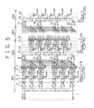
- Fig. 18 shows the configuration of a two-stage serial parallel type A/D converter described in Japanese Patent Laid-Open Publication No.Hei 3-157020.
- This A/D converter is a two-stage serial parallel type A/D converter which utilizes interpolation to perform A/D conversion in two stages consisting of an upper A/D conversion block 1831 and a lower A/D conversion block 1832.
- the A/D converter comprises a reference voltage generating circuit 1801 composed of a series of resistors, a differential amplifier row 1802, a sample/hold (S/H) circuit row 1803, comparator rows 1804 and 1812, a switch row 1805, an upper encoder 1806, S/H circuits 1807 and 1808, differential amplifiers 1809 and 1810, a resistive interpolation circuit 1811, and a lower encoder 1813.
- the differential voltages between individual reference voltages obtained from the reference voltage generating circuit 1801 and an analog input voltage are amplified by the differential amplifier row 1802.
- the differential voltages are sampled/held by the S/H circuit row 1803.
- the differential voltages held by the S/H circuit row 1803 are compared in the comparator row 1804.
- the outputs of the comparator row 1804 are converted into binary digital code by the upper encoder 1806, obtaining an upper A/D conversion result 1821.
- the upper encoder 1806 generates a control signal CTL for turning on certain switches in the switch row 1805, so that differential voltages with two reference voltages in the vicinity of the input voltage, out of the differential voltages held by the S/H circuit row 1803 are transferred to the lower A/D conversion block 1832.
- the two differential voltages transferred are sampled/held by the S/H circuits 1807 and 1808.
- the noninverted outputs and inverted outputs of the differential amplifiers 1809 and 1810 are individually interpolated by the resistive interpolation circuit 1811.
- the resulting interpolated voltages are compared in the comparator row 1812.
- the lower encoder 1813 converts the outputs of the comparator row 1812 into binary digital code to obtain a lower A/D conversion result 1822.
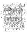
- a signal 1901 is a signal of the S/H circuit row 1803.
- a signal 1902 is a signal of the comparator row 1804.
- a signal 1903 is a signal of the selector switch 1805.
- a signal 1904 is a signal of the S/H circuits 1807 and 1808.
- a signal 1905 is a signal of the comparator row 1812.
- the signals 1901 and 1902 are signals 1911 of the upper A/D conversion block 1831.
- the signals 1904 and 1905 are signals 1912 of the lower A/D conversion block 1832.
- a conversion cycle 1921 of the A/D converter is the sum of period a1, b1, and c1.
- the held voltage is settled in the period b1.
- the comparator row 1804 starts its comparing operation in the period b1, and outputs the result in the period c1.
- the encoder 1806 generates the upper A/D conversion result 1821 and a control signal CTL from the comparison outputs, and keeps certain switches 1805 on over the period c1.
- the S/H circuits 1807 and 1808 are in a sample mode.
- the S/H circuits 1807 and 1808 change to a hold mode in the period a2.
- the S/H circuit row 1803 returns to the sample mode.
- the outputs of the interpolation circuit 1811 are settled in the period a2 before the comparator row 1812 starts its comparing operation.
- the encoder 1813 outputs the lower A/D conversion result 1822 at the period b2. It is the operating speed of the S/H circuit row 1803 that determines the conversion speed (sampling frequency) of the A/D converter.
- the sum of the periods a1, b1, and c1 fixes the conversion cycle of this A/D converter.
- the interpolation type two-stage serial parallel scheme shown in Fig. 18 has the following problems.
- a rise in the number of bits to be converted in the lower stage increases the number of interpolation nodes by power of 2.
- the settling time of the interpolation voltage is determined by the time constant between the load capacitance and the interpolation resistance of that interpolation node.
- the greater the number of bits to be converted in the lower stage the slower the operating speed of the interpolation circuit becomes.
- the interpolating operations therefore fail to follow the changes of the differential voltages transferred from the upper A/D conversion block, deteriorating the conversion accuracy in the lower stage.
- the S/H circuit row 1803 must remain in the hold mode until differential voltages are transferred to the lower A/D conversion block completely. This fixes the conversion speed of the A/D converter as shown in Fig. 19.
- the comparator row 1804 starts comparisons in the period b1.
- This comparison start timing is preferably set as close to the end of period b1 as possible, considering the sufficient settling of the hold voltages in the S/H circuit row 1803.
- the encoder 1806 inevitably has a circuit-operation delay time before generating the control signal CTL for the switches 1805 out of the comparison outputs of the comparator row 1804. Therefore, if the comparison start timing is set too closer to the end of the period b1, the switches 1805 for transferring the differential voltages from the upper A/D conversion block 1831 to the lower A/D conversion block 1832 come to be turned on in the middle of the period c1, with a reduction in the actual transfer time.
- the differential voltages to be transferred to the lower A/D conversion block 1832 may not be settled sufficiently, contributing to a deterioration in the conversion accuracy of the lower A/D conversion block 1832.
- the hold time of the S/H circuit row 1803, for the sake of preventing a deterioration in conversion accuracy, must be made longer than the sum total of the settling time of the hold voltages in the S/H circuit row 1803, the operation delay time of the encoder 1806, and the acquisition time of the S/H circuits 1807 and 1808 in the lower A/D conversion block 1832. This determines the conversion speed with respect to conversion accuracy.
- the offset voltages occur in a random fashion due to such reasons as element variations and asymmetry in layout, and still vary by several to ten-odd millivolts even if the transistors are designed with greater size.
- A/D converters have an LSB as extremely small as several millivolts.
- the input offset voltages can easily deteriorate the conversion accuracy. Therefore, the correction of the input offset voltages leads to higher accuracy.
- EP-A-0 414 389 discloses a sample/hold circuit according to the preamble of claim 1, used in an A/D converter.
- a plurality of different reference voltages are generated.
- a set of differential conversion circuits has first input terminals subjected in common to an analog input signal and second input terminals subjected to the respective reference voltages, and converts differences between voltages at the first and second input terminals into differential output voltages.
- a first A/D conversion circuit compares the analog input signal with the reference voltages to perform a higher-order A/D conversion of the input analog signal. At least two of the differential output voltages are selected. An interval between the selected differential output voltages is divided, and divided voltages are generated in accordance with the division.
- a second A/D conversion circuit compares the divided voltages to perform a lower-order A/D conversion of the analog input signal.
- EP-A-0 281 155 discloses a multi-stage A/D converter having a first A/D converter for A/D-converting an input signal and determining upper bits of the n-bit binary code, first and second sample-hold circuits which are alternately switched each time the first A/D converter samples the analog input signal, for sampling and holding the analog input signal, in synchronism with a sampling timing of the first A/D converter, and a second A/D converter.
- the second A/D converter is constituted by a reference voltage generator for generating reference voltages based on contents of the binary code obtained by the first A/D converter, a voltage comparator for comparing the reference voltage with a voltage value of the analog input signal held in one of the first and second sample-hold circuits, which sample and hold the analog input signal corresponding to the binary code, and an encoder for encoding a comparison result output from the voltage comparator and determining lower bits of the n bits.
- a sample/hold circuit used in a multi-stage A/D converter and comprising: a reference voltage generating circuit for generating a plurality of reference voltages; a differential amplifier row including a plurality of differential amplifiers for receiving an analog input voltage of said multi-stage A/D converter at first input terminals and said individual reference voltages generated by said reference voltage generating circuit at other input terminals, amplifying differential voltages between said analog input voltage and said individual reference voltages and outputting the resultant individual differential voltages between noninverted output terminals and inverted output terminals as potential differences; and a first sample/hold circuit row including a plurality of first sample/hold circuits for sampling/holding said individual differential voltages output from said differential amplifier row; characterized by: a second sample/hold circuit row for performing interleaving operations, having a pair of second and third sample/hold circuits connected to each output of said first sample/hold circuit row.
- An embodiment of the present invention may provide an A/D converter of higher speed.
- An embodiment of the present invention may provide an A/D converter of higher accuracy.
- An embodiment of the present invention may provide an A/D converter of lower power consumption.
- a multi-stage A/D converter embodying the invention comprises, in addition to the above sample/hold circuit, a first comparator row including a plurality of comparators for determining whether the individual differential voltages held by the first sample/hold circuit row are positive or negative; and a first encoder for outputting digital code corresponding to the outputs of the first comparator row.
- the second sample/hold circuit row includes the second and third sample/hold circuits which are connected in parallel to each output of the first sample/hold circuit row.
- the third sample/hold circuits are brought into a hold mode so that the sample/hold circuits for sampling are alternated at conversion cycles.
- the alternation of the sample/hold circuits for sampling allows an increase in A/D conversion speed. Since a stable hold time can be secured, it is possible to realize an A/D converter of higher accuracy.
- Figs. 1A-1C are block diagrams showing configuration examples of A/D converters according to a first embodiment of the present invention.
- Fig. 1A shows a first configuration example of an 8-bit A/D converter.
- This A/D converter comprises a first stage A/D conversion block 102, a second stage A/D conversion block 103, a third stage A/D conversion block 104, and a digital signal processor (DSP) 101.
- the first stage A/D conversion block 102 has a 4-bit configuration
- the second stage A/D conversion block 103 a 2-bit configuration
- the third stage A/D conversion block 104 a 2-bit configuration.
- the DSP 101 receives 4-bit, 2-bit, and 2-bit digital signals from the three conversion blocks 102, 103, and 104, respectively, and outputs an 8-bit digital signal.
- Fig. 1B shows a second configuration example of an 8-bit A/D converter.
- This A/D converter comprises a first stage A/D conversion block 112, a second stage A/D conversion block 113, a third stage A/D conversion block 114, a fourth stage A/D conversion block 115, and a DSP 111.
- the first stage A/D conversion block 112 has a 2-bit configuration
- the second stage A/D conversion block 113 a 2-bit configuration
- the third stage A/D conversion block 114 a 2-bit configuration
- the fourth stage A/D conversion block 115 a 2-bit configuration.
- the DSP 111 receives 2-bit, 2-bit, 2-bit, and 2-bit digital signals from the four conversion blocks 112, 113, 114, and 115, respectively, and outputs an 8-bit digital signal.
- Fig. 1C shows a configuration example of a 10-bit A/D converter.
- This A/D converter comprises a first stage A/D conversion block 122, a second stage A/D conversion block 123, a third stage A/D conversion block 124, a fourth stage A/D conversion block 125, and a DSP 121.
- the first stage A/D conversion block 122 has a 4-bit configuration
- the second stage A/D conversion block 123 has a 2-bit configuration
- the third stage A/D conversion block 124 a 2-bit configuration
- the fourth stage A/D conversion block 125 a 2-bit configuration.
- the DSP 121 receives 4-bit, 2-bit, 2-bit, and 2-bit digital signals from the four conversion blocks 122, 123, 124, and 125, respectively, and outputs a 10-bit digital signal.
- Fig. 2 is a circuit diagram of an A/D converter according to the present embodiment.
- This A/D converter is a 4-bit A/D converter, having a first stage for 2-bit A/D conversion, a second stage for 1-bit A/D conversion, and a third stage for 1-bit A/D conversion in a three-stage cascade connection.
- a reference voltage generating circuit 1 consists of a resistance element row, and generates new reference voltage levels VR 1 -VR 5 from two reference voltages VRL and VRH.
- the minimum voltage level of an analog input corresponds to VR 1
- the maximum voltage level to VR 5 .
- the full scale range of this A/D converter is (VR 5 - VR 1 ).
- VRL and VRH are used to generate the voltage levels to be input to differential amplifiers 11 and 8 when an analog input voltage is in the vicinities of VR 1 and VR 5 , respectively.
- a differential amplifier row 2 consists of seven differential amplifiers.
- the differential amplifiers receive an analog input voltage VIN at the positive input terminals, and the individual reference voltages at the negative input terminals.
- the differential amplifiers linearly amplify differential voltages obtained by subtracting the reference voltages from the analog input voltage, and output the resultant through their noninverted and inverted outputs as potential differences.
- a S/H circuit row 3 consists of seven S/H circuits, and samples/holds the noninverted and inverted output voltages from the differential amplifier row 2 at conversion cycles.
- a S/H circuit row 4 consists of 14 S/H circuits.
- the S/H circuits SHA sample the noninverted and inverted outputs of the S/H circuit row 3.
- the S/H circuits SHB are in a hold mode.
- the S/H circuit row 3 holds next differential voltages, which are sampled by the S/H circuits SHB.
- the S/H circuits SHA are in a hold mode.
- the S/H circuits SHA and SHB take turns to sample the outputs of the S/H circuit row 3 at conversion cycles.
- a comparator row 5 consists of five comparators, and compares noninverted and inverted outputs of the S/H circuit row 3 in magnitude. Then, it outputs signals that indicate positive if noninverted outputs > inverted outputs, and negative if noninverted outputs ⁇ inverted outputs.
- the comparison outputs are transmitted to an encoder 6.
- the encoder 6 makes the determination (referred to as boundary determination) that the analog input voltage level VIN falls within the range of VR k ⁇ VIN ⁇ VR k+1 (k is an integer in the range of 1 and 4), it outputs, according to the determination, a first stage A/D conversion result 201 in the form of 2-bit digital code.
- the encoder 6 Based on the determination, the encoder 6 also generates a control signal CTL for turning on selector switches 7 so that the noninverted output terminals and inverted output terminals of the S/H circuits SHA(B) k-1 , SHA(B) k , SHA(B) k+1 , and SHA(B) k+2 (k is an integer in the range of 1 and 4) that hold the differential voltages the comparator row 5 used in the comparison are connected to the positive input terminals and negative input terminals of the differential amplifiers 11, 10, 9, and 8 in the second stage, respectively.
- the reason why the voltages of the S/H circuits SHA(B) k-1 and SHA(B) k+2 are also transferred is as follows.
- the boundary determination error can be buffered as far as the adjacent boundaries.
- the following shows an example of operation of the first stage. Assuming that the analog input VIN falls within the range of VR 2 ⁇ VIN ⁇ VR 3 , the outputs of the differential amplifiers PA 0 -PA 2 have the relationship that noninverted output > inverted output. In contrast, the outputs of the differential amplifiers PA 3 -PA 6 have the relationship that noninverted output ⁇ inverted output. These relationships also hold for the differential outputs of the S/H circuit row 3.
- the comparator row 5 makes a determination on these relationships, and sends the comparisons to the encoder 6 in the form of positive/negative signals.
- the encoder 6 Based on the comparisons sent from the comparator row 5, the encoder 6 detects that the analog input voltage level VIN falls within the range of VR 2 ⁇ VIN ⁇ VR 3 (in this case, the comparators made accurate positive/negative determinations), and outputs 2-bit digital code of "01." At the same time, the encoder 6 generates a control signal CTL for turning on selector switches 7 so that the noninverted output terminals and inverted output terminals of the S/H circuits SHA 1 , SHA 2 , SHA 3 , and SHA 4 are connected to the positive input terminals and negative input terminals of the differential amplifiers 11, 10, 9, and 8 in the second stage, respectively.
- a resistive interpolation circuit 12 consists of twelve resistance elements.
- the noninverted and inverted outputs of the differential amplifiers 8 and 9, the noninverted and inverted outputs of the differential amplifiers 9 and 10, and the noninverted and inverted outputs of the differential amplifiers 10 and 11 are respectively divided by the resistances, and interpolated for a single bit to generate interpolation nodes of voltages V ilpm and V ilnm (m is an integer in the range of 0 and 6).
- a S/H circuit row 13 consists of 14 S/H circuits.
- the S/H circuits SHC and SHD sample the outputs V ilpm and V ilnm of the interpolation circuit 12 alternately at conversion cycles.
- a comparator row 14 consists of five comparators, and compares the voltages V ilpm and V ilnm in magnitude.
- the differential amplifiers 8 and 9 have the relationship that noninverted output ⁇ inverted output
- the differential amplifiers 10 and 11 the relationship that noninverted output > inverted output.
- the interpolation nodes that satisfy V ilpm ⁇ V ilnm come between the differential amplifiers 9 and 10. If any boundary determination error is made by the encoder 6, however, the nodes come either between the differential amplifiers 8 and 9 or between the differential amplifiers 10 and 11.
- an encoder 15 Based on the outputs of the comparator row 14, an encoder 15 detects the boundary across which the voltages V i1pm and V i1nm are reversed in magnitude relationship. If that boundary is determined to fall between the differential amplifiers 9 and 10, the encoder 15 outputs a second stage A/D conversion result 202, or 1-bit digital code.
- the 1-bit digital code, the second stage A/D conversion result 202 is output to the DSP 101, 111, or 121 of Figs. 1A-1C, along with code for digitally correcting the least significant one bit of the 2-bit digital code which is the first stage A/D conversion result 201.
- the DSP 101, 111, or 121 digitally corrects the least significant one bit mentioned above.
- the encoder 15 generates a control signal CTL for turning on selector switches 16 so that the noninverted output terminals and inverted output terminals of the S/H circuits SHC(D) m-1 , SHC(D) m , SHC(D) m+1 , and SHC(D) m+2 (m is an integer in the range of 1 and 4) that hold the interpolation voltages the comparator row 14 used in the comparison are connected to the positive input terminals and negative input terminals of differential amplifiers 20, 19, 18, and 17 in the third stage, respectively.
- the differential amplifiers 17-20 amplify the voltages transferred from the second stage through the selector switches 16, and output the resultant through the noninverted and inverted outputs as potential differences.
- a resistive interpolation circuit 21 consists of twelve resistance elements. The noninverred and inverted outputs of the differential amplifiers 17 and 18, the noninverted and inverted outputs of the differential amplifiers 18 and 19, and the noninverted and inverted outputs of the differential amplifiers 19 and 20 are respectively divided by the resistances, and interpolated for a single bit to generate interpolation nodes of voltages V i2pm and V i2nm (m is an integer in the range of 0 and 6).
- a comparator row 22 consists of five comparators, and compares the voltages V i2pm and V i2nm in magnitude.
- the differential amplifiers 17 and 18 have the relationship that noninverted output ⁇ inverted output, and the differential amplifiers 19 and 20 the relationship that noninverted output > inverted output.
- the interpolation nodes that satisfy V i2pm ⁇ V i2nm come between the differential amplifiers 18 and 19. If any boundary determination error is made by the encoder 15, however, the nodes come either between the differential amplifiers 17 and 18 or between the differential amplifiers 19 and 20.
- an encoder 23 From the outputs of the comparator row 22, an encoder 23 detects the boundary across which the voltages V i2pm and V i2nm are reversed in magnitude relationship. If that boundary is determined to fall between the differential amplifiers 18 and 19, the encoder 23 outputs a third stage A/D conversion result 203, or 1-bit digital code.
- the 1-bit digital code, the third stage A/D conversion result is output to the DSP 101, 111, or 121 of Figs. 1A-1C, along with code for digitally correcting the least significant one bit of the 1-bit digital code which is the second stage A/D conversion result.
- the DSP 101, 111, or 121 determines the total sum of the A/D conversion outputs 201, 202, and 203 from the individual stages, and performs necessary correction to obtain a 4-bit A/D conversion result for the analog input VIN. For example, when first-stage digital code of "01,” second-stage digital code of "1,” and third stage digital code of "0" are output for a certain analog input, and no digital correction occurs in the second and third stages, the 4-bit digital code for that analog input is "0110.”
- Fig. 3 is an operation timing chart of the A/D converter.
- a signal 301 is a signal of the S/H circuit row 3.
- a signal 302 is a signal of a S/H circuit SHA in the S/H circuit row 4.
- a signal 303 is a signal of a S/H circuit SHB in the S/H circuit row 4.
- a signal 304 is a signal of the comparator row 5.
- a signal 305 is a signal of a selector switch 7.
- a signal 306 is a signal of the comparator row 14.
- the total of periods a1 and b1 is a conversion cycle 307 of the A/D converter.
- the signal 301 alternates between sample and hold at equal intervals.
- the S/H circuit row 3 As soon as the S/H circuit row 3 is switched from a sample mode to a hold mode to settle its hold voltages in the period b1, half the S/H circuits in the S/H circuit row 4 sample the hold voltages.
- the comparator row 5 starts its comparing operations immediately before the end of the period b1, and outputs the comparisons in the period a2.
- the encoder 6 completes operation based on the comparisons.
- the encoder 6 outputs the first stage A/D conversion result in the period b2, and generates a control signal CTL to turn certain switches 7 on over the periods b2 and a3, transferring differential voltages from the first stage to the second stage.
- the outputs of the interpolation circuit 12 are settled in the periods b2-a3 before the comparator row 14 starts comparing operations. From the comparisons, the encoder 15 outputs the second A/D conversion result in the period b3. Meanwhile, in the period a2, the S/H circuit row 3 reenters a sample mode. The S/H circuit row 3 is switched into a hold mode in the period b2, so that the other S/H circuits in the S/H circuit row 4 make the same operations as described above. It is the operating speed of the S/H circuit row 3 that determines the conversion speed (sampling frequency) of the A/D converter. Thus, as shown in Fig. 3, the sum of the periods a1 and b1 fixes a conversion cycle 307 of the A/D converter.
- the S/H circuit row 4 is inserted with aims as follows:
- the present embodiment achieves conversion speed at least twice or much higher than that of the conventional scheme while securing the same transferring time.
- FIG. 4 shows a configuration example of an A/D converter having a two-stage configuration.
- This A/D converter has a first stage A/D conversion block 401 and a second stage A/D conversion block 402.
- An encoder 6 outputs a conversion result 201 of the first stage A/D conversion block 401.
- An encoder 15 outputs a conversion result 202 of the second stage A/D conversion block 402.
- Fig. 5 shows a configuration example of a multistage cascade interpolation type A/D converter having a k-stage configuration.
- k is an integer not smaller than 2, which means an A/D converter having two or more stages.
- This A/D converter comprises a first stage A/D conversion block 501, a second stage A/D conversion block 502, third to (k-1)th stage A/D conversion blocks 503, and a kth stage A/D conversion block 504.
- the k stages (k is an integer greater than or equal to 2) of A/D conversion blocks are cascaded.
- the second and subsequent stages each perform A/D conversion only on data interpolations sent from the A/D conversion blocks at their immediate upper stages.
- two S/H circuits which operate at cycles twice as long as the conversion cycles are inserted in parallel for each reference voltage level or interpolation voltage level, so as to perform sampling alternately at the conversion cycles.
- Figs. 1A-1C show configuration examples of 8-bit and 10-bit A/D converters.
- the present embodiment it is possible to constitute an A/D converter of higher speed, higher resolution, and lower power consumption.
- the A/D conversion blocks advantageously have S/H circuit rows for operating at cycles twice the conversion cycles, inserted immediately before the respective selector switches.
- Fig. 6 shows an A/D converter according to a second embodiment of the present invention.
- a differential amplifier row 2 in the present embodiment has one extra differential amplifier as compared with the differential amplifier row 2 in the first embodiment shown in Fig. 2.
- This differential amplifier row 2 is a differential amplifier row on the input front end of the A/D converter.
- the individual differential amplifiers 24-31 of the differential amplifier row 2 have the circuit configuration of Fig. 8A.
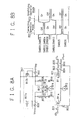
- Fig. 8A is a circuit diagram of a differential amplifier according to the second embodiment.
- a differential pair transistor (hereinafter, referred to as differential pair) 811 has n-channel MOS transistors 811a and 811b.
- a differential pair 813 has n-channel MOS transistors 813a and 813b.
- P-channel MOS transistors 817a and 817b have their gates and drains connected to each other, functioning as resistors.
- the resultant resistors 817a and 817b constitute an output resistance circuit (load circuit) 817.
- the differential pair 811 functions as an input unit in an amplifying operation mode.
- the differential pair 813 shares the individual drain terminals with the differential pair 811.
- Capacitance elements 815 and 816 are connected to between the respective gate terminals of the differential pair 813 and a ground.
- the output resistance circuit 817 is connected to the shared drain terminals of the differential pairs 811 and 813.
- Switches 807 and 808 can short the differential output terminals and the respective gate terminals of the differential pair 813.
- Switches 801, 803-806, 809, and 810 can switch inputs/outputs depending on whether an amplifying operation mode or an offset correcting operation mode.
- Fig. 8B shows ON/OFF control signals for the switches in an offset correcting operation mode 821 and an amplifying operation mode 822.
- the high and low levels represent ON and OFF states, respectively.
- the switches 801, 803, 809, and 810 are turned off.
- the switches 802, 804, 807, and 808 are turned on.
- the switches 805 and 806 are kept so that either of them is always in an ON state.
- the switches are changed over in entering a correcting operation. Once changed over, they keep their states until the next correcting operation.
- VRL or VRH reference voltage
- the correcting and amplifying operations will be described in sequence.
- symbols gm1 and gm2 represent the transconductances of the differential pairs 811 and 813, respectively.
- Symbols V off1 and V off2 represent the input offset voltages of the differential pairs 811 and 813 resulting from element variations, respectively.
- the time for a correcting operation mode is set to be several times longer than a sampling cycle (conversion cycle).
- a reference voltage VR n+1 is input to both gate terminals of the differential pair 811.
- the aim of the switch 803 is to match the numbers of switches to be connected to both gate terminals of the differential pair 811 so that switch-originated charge injection noise at both gate terminals balances as closely as possible.
- the capacitors 815 and 816 are provided with a capacitance not smaller than several hundreds of femtofarads. If this capacitance is greater and requires longer time for the negative feedback operation, the time for the correcting operation mode is extended accordingly.
- the switches 802, 804 are turned off and the switches 801, 803 are turned on so that the analog input VIN and the reference voltage VR n+1 are input to the gate terminals of the differential pair 811. Meanwhile, the switches 807 and 808 are turned off to eliminate the negative feedback. Even after the switches 807 and 808 are turned off, the capacitors 815 and 816 maintain the gate terminals A and B of the differential pair 813 to the voltages at the completion of the correcting operation.
- V offset 1 1 + g m 2 ⁇ R V off 1 + g m 2 g m 1 1 + g m 2 ⁇ R V off 2
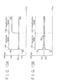
- Fig. 13A shows the time variations of voltages V INP and V INN in a correction mode 1301 and an amplification mode 1302.
- Fig. 13B shows the time variations of voltages V A and V B in a correction mode 1311 and an amplification mode 1312.
- the voltage V INP is the voltage on the gate of the transistor 811a.
- the voltage V INN is the voltage on the gate of the transistor 811b.
- the voltage V A is the voltage on the gate of the transistor 813a.
- the voltage V B is the voltage on the gate of the transistor 813b.
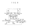
- Fig. 9 shows the state of connection of the differential amplifiers in an offset correcting operation mode.
- the switches 802, 804, 806, 807, and 808 are turned on.
- the other switches are turned off.
- the differential pair 811 receives VR at both inputs.
- the differential outputs are shorted to the inputs of the differential pair 813, thereby forming negative feedback.
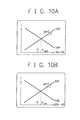
- Fig. 10A shows an example of the voltage-current characteristic of the differential pair 813.
- Fig. 10B shows an example of the voltage-current characteristic of the differential pair 811.
- the offset voltages of the differential pairs 811 and 813 are V off1 and V off2 , respectively.
- V off1 is referred to as input offset voltage (more specifically, input conversion offset voltage).
- the currents Id1, Id2, Id3, and Id4 to flow through the transistors 811a, 811b, 813a, and 813b are given by the following equations (5) - (8):
- I d 1 g m 1 ⁇ V R n + 1
- I d 2 g m 1 ⁇ ( V R n + 1 + V off 1 )
- I d 3 g m 2 ⁇ V A
- I d 4 g m 2 ⁇ ( V B + V off 2 )
- voltages V C and V D are expressed by the following equations (9) and (10), where R is the resistance of the output resistance circuit 817.
- the voltage V C is the voltage on the drain of the transistor 813a.
- the voltage V D is the voltage on the drain of the transistor 813b.
- V A - V B a potential difference V A - V B in the differential pair 813 is given by the following equation (13).
- the equation (13) traces the voltage 815 of Fig. 13B.
- V A ⁇ V B g m 1 ⁇ V off 1 1 R + g m 2 + g m 2 ⁇ V off 2 1 R + g m 2
- V A ⁇ V B g m 1 g m 2 V off 1 + V off 2
- the voltages V A and V B are held by the capacitors 815 and 816, respectively.
- Fig. 11 shows the state of connection of the differential amplifiers in an amplifying operation mode.
- the switches 801, 803, 806, 809, and 810 are turned on. The other switches are turned off.
- the inputs of the differential pair 811 receive VIN and VR.
- the differential outputs are subsequently connected to a S/H circuit in the next stage.
- the voltages of the individual nodes are given by the following equations (15)-(18).
- the voltage V INP is the voltage on the gate of the transistor 811a.
- the voltage V INN is the voltage on the gate of the transistor 811b.
- the voltage V C is the voltage on the drain of the transistor 813a.
- the voltage V D is the voltage on the drain of the transistor 813b.
- V c V o n
- V D v o p
- the voltages V A and V B are maintained at the values given by the equations (11) and (12), respectively.
- the currents Id1, Id2, Id3, and Id4 flowing through the transistors 811a, 811b, 813a, and 813b are given by the following equations (19)-(22) :
- I d 1 g m 1 ⁇ V IN
- I d 2 g m 1 ⁇ ( V R n + 1 + V off 1 )
- I d 3 g m 2 ⁇ V A
- I d 4 g m 2 ⁇ ( V B + V off 2 )
- the first term shows that the differential input voltage appears constant-fold in the differential output voltage. That is, gm1 x R is the gain of this differential amplifier.
- the second and third terms are offset terms appearing on the output.
- An input offset voltage V offset is determined by dividing the second and third terms by the gain (gm1 x R), or from the following equation (26) :
- V offset 1 1 + g m 2 ⁇ R V off 1 + g m 2 g m 1 1 + g m 2 ⁇ R V off 2
- This equation (26) is equivalent to the above-described equation (1), and is shown in Fig. 12B.
- Fig. 6 shows a situation where the differential amplifier 31 is in a correcting operation and the differential amplifiers 24-30 are in an amplifying operation.
- the differential voltages between the analog input voltage VIN and the individual reference voltages VRL, VR 1 , VR 2 , VR 3 , VR 4 , VR 5 , and VRH are amplified by the differential amplifiers 24, 25, 26, 27, 28, 29, and 30, respectively.
- the differential amplifier 31 receives VRH at both inputs of the differential pair, performing the correcting operation. Switches on the output sides of the differential amplifiers are controlled so that the outputs of the differential amplifiers 24-30 are sampled/held by the S/H circuits 32-38, respectively. The outputs of the differential amplifier 31 are switched away from the S/H circuit row 3.
- the differential amplifier 31 completes its correcting operation. Then, the switches on the output side of the differential amplifiers are controlled when the S/H circuit row 3 is in a hold mode, so that the differential amplifier 31 is connected to the S/H circuit 38 and the outputs of the differential amplifier 30 are separated from the S/H circuit row 3. At the same time, a reference voltage to be input to the differential amplifier 30 is changed from VRH to VR 5 . This supplies VR 5 to both inputs of the differential pair so that the differential amplifier 30 starts its correcting operation. The differential amplifier 31 returns to an amplifying operation mode, amplifying the differential voltage between the analog input voltage VIN and the reference voltage VRH. After another certain period of time, the differential amplifier 29 in turn enters a correcting operation.
- Correcting operations are performed successively in descending order across the differential amplifier row. Upon completion of the correcting operation at the bottom, the correcting operations simply turn around to be successively performed in ascending order this time. On completion at the top end, the correcting operations turn around again to be successively performed in descending order. In this way, the operations are consecutively repeated in a relay fashion. This aims to reduce the number of switches to be operated for switching the inputs/outputs of the differential amplifiers.
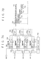
- Fig. 7A shows a simplified partial circuit of the A/D converter in Fig. 6.
- reference voltages VR1, VR2, and VR3 are generated.
- the reference voltage VR1, VR2, and VR3 each are input to one of differential amplifiers 701-704 through switches 707 and 708.
- a control circuit 706 exercises ON/OFF control of the switches 707, 708, and 709.
- the differential amplifier 701 is in a correcting operation mode, and the differential amplifiers 702-704 are in an amplifying operation mode.
- the differential amplifier 701 receives the reference voltage VR3 at both the positive input terminal and negative input terminal thereof.
- the differential amplifier 702 receives the analog voltage VIN and the reference voltage VR3.
- the differential amplifier 703 receives the analog voltage VIN and the reference voltage VR2.
- the differential amplifier 704 receives the analog voltage VIN and the reference voltage VR1.
- the differential amplifiers 701-704 output their differential outputs to a S/H circuit row 705 through the switch 709.
- the S/H circuit row 705 contains S/H circuits 705a, 705b, and 705c.
- the outputs of the differential amplifier 701 are disconnected from the S/H circuit row 705.
- the outputs of the differential amplifier 702 are connected to the S/H circuit 705a.
- the outputs of the differential amplifier 703 are connected to the S/H circuit 705b.
- the outputs of the differential amplifier 704 are connected to the S/H circuit 705c.
- Fig. 7B is a timing chart showing the operations of the A/D converter in Fig. 7A.
- the sampling clock 721 of the S/H circuit row 705 has a conversion cycle 722.
- the differential amplifiers 701-704 switch between correcting and amplifying operation modes.
- the differential amplifier 701 enters a correcting operation mode
- the other differential amplifiers 702-704 enter an amplifying operation mode.
- only the differential amplifier 702 enters a correcting operation mode; at a period 733, only the differential amplifier 703; and at a period 734, only the differential amplifier 704.
- differential amplifiers with correcting/amplifying operation modes are configured as shown in Fig. 8A.
- at least one extra differential amplifier having this configuration is added to the minimum number of differential amplifiers required in the first stage A/D conversion, so that at any point of time the added differential amplifier(s) is/are operated in a correcting operation mode while the other differential amplifiers are in an amplifying operation mode.
- adjoining differential amplifiers are switched into a correcting operation mode in a temporally continuous manner, whereby the differential amplifiers repeat amplification ⁇ correction ⁇ amplification ⁇ ... in a relay fashion.
- the series of operations is controlled by the control circuit.
- Fig. 8A Configuring the differential amplifiers as shown in Fig. 8A allows the correction of input offset voltages.
- the capacitance elements for holding correction voltages are connected to the differential pair 813. Since these capacitance elements are not directly visible from the analog input terminal, the capacitances can be increased in order to reduce leakage of charge.
- the input capacitance seen from the analog input terminal is a gate capacitance of the differential pair 811, and is very much smaller, depending on the transistor size of the differential pair.
- the differential amplifiers having the configuration of Fig. 8A make their amplifying operations and correcting operations independently. Differential amplifiers in a correcting operation are thus incapable of functioning as part of the A/D converter. Then, as shown in Fig. 7A, ⁇ extra differential amplifiers ( ⁇ ⁇ 1) with respect to the number of reference voltage levels are added to constitute the differential amplifier row, and the ⁇ differential amplifiers 701 in a correcting operation mode are temporarily separated from the A/D converter. After a certain correcting-operation time, another ⁇ differential amplifiers are isolated from the A/D converter into a correcting operation mode. This method eliminates the need for suspending the A/D conversion operation for the sake of correcting operations (that is, no deterioration in conversion speed). It also allows sufficient correction time to be secured irrespective of the sampling cycle (conversion cycle) as shown in Fig. 7B.
- the A/D converter described in the present embodiment is configured so that the S/H circuit row 3 comes immediately after the differential amplifier row 2 on the input front end. Therefore, amplifying and correcting operations can be switched at the time of holding of the S/H circuit row 3, thereby precluding switching noise occurring on the switching.
- Fig. 14 shows a differential amplifier according to a third embodiment of the present invention.
- Switches 801-810 make the same operations as in the second embodiment.
- description will be given of the operations of an output resistance circuit (load circuit) 1425 under correcting and amplifying operations in sequence.
- gm3 is the transconductance between the transistors 1421 and 1424
- gm4 is the transconductance between the transistors 1422 and 1423.
- the switches 1417 and 1418 are turned off, and the switches 1419 and 1420 are turned on. This disconnects the drain terminals of the transistors 1422 and 1423 from the differential output terminals.
- the gate terminals and source terminals of the same are shorted to nullify the gate-to-source voltages for a nonconducting state.
- the output resistance circuit comes to have the configuration as that of Fig. 8A.
- V A ⁇ g m 1 ⁇ R a ⁇ V R n + 1 1 + g m 2 ⁇ R a
- V B ⁇ g m 1 ⁇ R a ⁇ ( V R n + 1 + V off 1 ) + g m 2 ⁇ R a ⁇ V off 2 1 + g m 2 ⁇ R a
- ⁇ V out g m 1 ⁇ R b ⁇ ⁇ V in ⁇ g m 1 ⁇ R b ⁇ V off 1 1 + g m 2 ⁇ R a ⁇ g m 2 ⁇ R b ⁇ V off 2 1 + g m 2 ⁇ R a
- the input offset voltage in an amplifying operation is obtained by dividing the offset terms in the equation (34) by the gain gm1 x R in an amplifying operation, or as in the following equation (35) :
- V offset 1 1 + g m 2 ⁇ R a V off 1 + g m 2 g m 1 1 + g m 2 ⁇ R a V off 2
- differential amplifiers are configured so that their output resistance circuits can increase in output resistance only when in the correcting operation mode.
- This increase in output resistance provides the additional function of temporarily raising the direct-current gain in the correcting operation mode above that in the amplifying operation mode.
- the configuration as in Fig. 14A makes it possible to raise the output resistances only in correcting operations.
- the differential amplifiers increase in direct-current gain. That is, the configuration of Fig. 14A temporarily increases the direct-current gains of the differential amplifiers only in correcting operations.
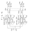
- Fig. 15 shows S/H circuits according to a fourth embodiment of the present invention.
- a S/H circuit 1540 is in a sample mode, and a S/H circuit 1550 is in a hold mode.
- the input terminals 1501p and 1501n are input terminals of the S/H circuit row 4 in Fig. 6.
- the S/H circuit 1540 corresponds to a S/H circuit SHA, and the S/H circuit 1550 a S/H circuit SHB.
- switches 1531p and 1531n in a switch 1530 are opened to break the connection between the S/H circuit 1540 and output terminals 1534p and 1534n.
- Wiring capacitances 1533p, 1533n lie between the output terminals 1534p, 1534n and a ground, respectively.
- switches 1532p and 1532n in a switch 1530 are closed to establish the connection between the S/H circuit 1550 and output terminals 1536p and 1536n.
- Wiring capacitances 1535p, 1535n lie between the output terminals 1536p, 1536n and a ground, respectively.
- the input terminal 1501p is connected to an input terminal inp of a differential amplifier 1510 through a switch 1511p and a capacitor 1512p.
- the input terminal 1501n is connected to an input terminal inn of the differential amplifier 1510 through a switch 1511n and a capacitor 1512n.
- An output terminal outn of the differential amplifier 1510 is connected through a switch 1514p to the input terminal inp, and through a switch 1513p to the interconnection node between the switch 1511p and the capacitor 1512p.
- An output terminal outp of the differential amplifier 1510 is connected through a switch 1514n to the input terminal inn, and through a switch 1513n to the interconnection node between the switch 1511n and the capacitor 1512n.
- a control signal from the encoder 6 or the like (Fig. 6) is input to the control terminal ctrl of the differential amplifier through a terminal 1516.
- the S/H circuit 1550 is identical to the S/H circuit 1540 described above, with a differential amplifier 1520 in place of the differential amplifier 1510. Since the S/H circuit 1540 is in a sample mode, the switches 1511p, 1511n, 1514p, and 1514n are closed and the switches 1513p and 1513n are opened. In contrast, the S/H circuit 1550 is in a hold mode, having the switches 1511p, 1511n, 1514p, and 1514n opened and the switches 1513p and 1513n closed.
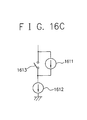
- Fig. 16A is a circuit diagram of the differential amplifier 1510.
- Fig. 16B is a circuit diagram of the differential amplifier 1520.
- the differential amplifiers 1510 and 1520 each have a current source Ibs for supplying a constant current to the coupled source terminals of the input differential pair, coupled with a single current source Ibh having a switch 1605 capable of switching on/off a current path thereof.
- a p-channel MOS transistor 1601 is connected at its source to a power supply voltage, and at its drain to the output terminal outn.
- a p-channel MOS transistor 1602 is connected at its source to the power supply voltage, and at its drain to the output terminal outp.
- the gates of the transistors 1601 and 1602 are both connected to a predetermined voltage terminal.
- An n-channel MOS transistor 1603 is connected at its drain to the output terminal outn, and at its gate to the input terminal inp.
- An n-channel MOS transistor 1604 is connected at its drain to the output terminal outp, and at its gate to the input terminal inn.
- the sources of the transistors 1603 and 1604 are connected to each other.
- the constant current source Ibs is connected at one end to the interconnection node between the sources of the transistors 1603 and 1604, and is grounded at the other end.
- the constant current source Ibh is connected at one end to the interconnection node between the sources of the transistors 1603 and 1604 through the switch 1605, and is grounded at the other end.
- the switch 1605 is controlled by the control signal from the encoder 6 or the like (Fig. 6) so as to switch on/off the current path.
- Fig. 16C is another configuration example of two current sources for supplying currents of two values.
- the current sources 1611, 1612 and the switch 1613 are used in Fig. 16C, while the current sources Ibs and Ibh are used in Figs. 16A and 16B.
- the current sources 1611 and 1612 are connected to each other in series.
- the switch 1613 is connected to the current source 1611 in parallel.
- the current source 1611 can supply current of a value 5
- the current source 1612 can supply current of a value 10.
- the switch 1613 By turning on the switch 1613 so as to make the serial connection of the switch 1613 and the current source 1612 a current path, current of a value 10 can be supplied.
- the capacitances 1533p, 1533n, 1535p, and 1535n are the input capacitances of the respective terminals in the next stage.
- Fig. 15 shows a situation where the switches 1532p and 1532n in the selector switch 1530 transfer data of the S/H circuit 1520 to the next stage.
- the switch 1605 for supplying the current source Ibh in the differential amplifier 1520 is turned on to provide a bias current of Ibs + Ibh.
- Fig. 17 shows time variations of the bias currents in the differential amplifier 1510 of the S/H circuit 1540 and the differential amplifier 1520 of the S/H circuit 1550.
- the bias current of the S/H circuit 1540 is shown to the top, and the bias current of the S/H circuit 1550 to the bottom.
- the S/H circuit 1540 enters a sample mode and the S/H circuit 1550 a hold mode.
- the S/H circuit 1540 enters a hold mode and the S/H circuit 1550 a sample mode.
- the periods 1701 and 1702 are repeated alternately.
- the S/H circuits 1540 and 1550 have a bias current 1722 of Ibs in a sample mode, and a bias current 1721 of Ibs + Ibh in a hold mode.
- the bias current in a hold mode can take two values 1721 and 1722.
- the bias current 1721 is for situations where the S/H circuit is in a hold mode and transfers data to the next stage.
- the switch 1605 turns on for a bias current value of Ibs + Ibh.
- the bias current 1722 is for situations where no data is transferred to the next stage. Since the switch 1605 does not turn on, the current has the same value Ibs as in a sample mode.
- N of the circuits are in a sample mode and the remaining N are in a hold mode.
- the remaining (N-4) circuits simply make holding operations.
- two S/H circuits are inserted in parallel into the front of each selector switch in the individual A/D conversion blocks.
- at least one current source having a switch for switching the current path on/off is connected to the coupled source terminals of an input differential pair in the differential amplifier constituting the S/H circuit, in parallel with a constant current source.
- only four S/H circuits that hold the four given differential voltages or interpolation voltages to be transferred to the next stage receive selector switch control signals generated by the encoder, turning on the switches in the differential amplifiers thereof.
- the differential amplifiers operate so as to temporarily increase in bias current only while transferring data to the next stage.
- the S/H circuits in front of the selector switches in each A/D conversion block are supposed to charge/discharge large load capacitances (mainly wiring capacitances) when connected to the next stage through the selector switches in a hold mode. Therefore, to ensure the operating speed of the S/H circuits, the differential amplifiers constituting the S/H circuits must be adjustable in bias current to values that ensure holding operations. In a sample mode, however, the load capacitances mentioned above are disconnected from the S/H circuits. The bias current values adjusted to ensure holding operations are therefore overspecified to sampling operations. Then, the differential amplifiers in the S/H circuits are configured as in Figs. 16A and 16B, so that the switches turn on to increase the bias current values at the time of holding alone. This can suppress the power consumption of the individual S/H circuits themselves while ensuring the speed of the holding operations.
- the number of S/H circuits in a S/H circuit row which are connected to the next stage through selector switches is only four all the time. Therefore, the differential amplifiers of the four circuits can be selectively and exclusively increased in bias current value to make a further reduction in the power consumption of the S/H circuit block.
- the second sample/hold circuit row includes the second and third sample/hold circuits connected in parallel to each output of the first sample/hold circuit row.
- the third sample/hold circuits are brought into a hold mode. In this way, the sample/hold circuits perform sampling in alternate conversion cycles.
- the alternation of the sample/hold circuits for sampling allows an increase in A/D conversion speed.
- stable hold time can be secured, it is possible to realize an A/D converter of higher accuracy.
Landscapes
- Engineering & Computer Science (AREA)
- Theoretical Computer Science (AREA)
- Analogue/Digital Conversion (AREA)
Applications Claiming Priority (2)
| Application Number | Priority Date | Filing Date | Title |
|---|---|---|---|
| JP2001067049A JP2002271201A (ja) | 2001-03-09 | 2001-03-09 | A/d変換器 |
| JP2001067049 | 2001-03-09 |
Publications (3)
| Publication Number | Publication Date |
|---|---|
| EP1239593A2 EP1239593A2 (en) | 2002-09-11 |
| EP1239593A3 EP1239593A3 (en) | 2004-01-21 |
| EP1239593B1 true EP1239593B1 (en) | 2006-08-30 |
Family
ID=18925457
Family Applications (1)
| Application Number | Title | Priority Date | Filing Date |
|---|---|---|---|
| EP01309751A Expired - Lifetime EP1239593B1 (en) | 2001-03-09 | 2001-11-20 | A/D converter |
Country Status (4)
| Country | Link |
|---|---|
| US (1) | US6480132B1 (enExample) |
| EP (1) | EP1239593B1 (enExample) |
| JP (1) | JP2002271201A (enExample) |
| DE (1) | DE60122669T2 (enExample) |
Families Citing this family (39)
| Publication number | Priority date | Publication date | Assignee | Title |
|---|---|---|---|---|
| TW564598B (en) * | 2001-07-13 | 2003-12-01 | Via Tech Inc | Data converter using active interpolation in background auto-zeroing |
| JP3851870B2 (ja) * | 2002-12-27 | 2006-11-29 | 株式会社東芝 | 可変分解能a/d変換器 |
| US7821555B2 (en) * | 2003-04-21 | 2010-10-26 | Micron Technology, Inc. | Multi path power for CMOS imagers |
| DE10337042B4 (de) * | 2003-08-12 | 2007-08-09 | Infineon Technologies Ag | Verfahren zur Umsetzung eines analogen Eingangssignals und Analog-Digital-Wandler |
| JP4529007B2 (ja) * | 2004-09-02 | 2010-08-25 | ルネサスエレクトロニクス株式会社 | 半導体集積回路装置 |
| US8059019B2 (en) * | 2005-01-25 | 2011-11-15 | Atmel Corporation | Method and system for minimizing the accumulated offset error for an analog to digital converter |
| ITRM20050086A1 (it) * | 2005-02-28 | 2006-09-01 | Uni Degli Studi Di Roma Tor Vergata | Convertitore analogico digitale. |
| US7394417B2 (en) * | 2005-06-10 | 2008-07-01 | Matsushita Electric Industrial Co., Ltd. | A/D converter |
| CN101310445A (zh) * | 2005-11-17 | 2008-11-19 | Nxp股份有限公司 | 折叠电路 |
| US7602326B2 (en) * | 2006-01-20 | 2009-10-13 | Oki Semiconductor Co., Ltd. | Digital-to-analog converter having resistor string with ranges to reduce circuit elements |
| JP4639153B2 (ja) * | 2006-01-20 | 2011-02-23 | Okiセミコンダクタ株式会社 | ディジタル・アナログ変換器 |
| KR101092116B1 (ko) * | 2007-02-22 | 2011-12-12 | 후지쯔 가부시끼가이샤 | 아날로그 신호 처리 장치 |
| WO2008146450A1 (ja) * | 2007-05-29 | 2008-12-04 | Mitsubishi Electric Corporation | アナログ入力装置 |
| JP5047699B2 (ja) * | 2007-06-08 | 2012-10-10 | ルネサスエレクトロニクス株式会社 | 増幅回路、デジタルアナログ変換回路及び表示装置 |
| FR2922388B1 (fr) * | 2007-10-12 | 2013-03-29 | Commissariat Energie Atomique | Quantificateur, convertisseur analogique-numerique comprenant un tel quantificateur, et recepteur ultra-large bande integrant un tel convertisseur |
| US7649488B1 (en) * | 2008-06-25 | 2010-01-19 | Aptina Imaging Corporation | Low-power column parallel cyclic analog-to-digital converter |
| JP2011109560A (ja) * | 2009-11-20 | 2011-06-02 | Fujitsu Semiconductor Ltd | アナログデジタル変換回路 |
| US9077386B1 (en) | 2010-05-20 | 2015-07-07 | Kandou Labs, S.A. | Methods and systems for selection of unions of vector signaling codes for power and pin efficient chip-to-chip communication |
| US9288082B1 (en) | 2010-05-20 | 2016-03-15 | Kandou Labs, S.A. | Circuits for efficient detection of vector signaling codes for chip-to-chip communication using sums of differences |
| JP2012163434A (ja) * | 2011-02-07 | 2012-08-30 | Rohm Co Ltd | 電池残量の検出回路、検出方法およびそれを用いた電子機器 |
| US10003315B2 (en) | 2016-01-25 | 2018-06-19 | Kandou Labs S.A. | Voltage sampler driver with enhanced high-frequency gain |
| US10003454B2 (en) | 2016-04-22 | 2018-06-19 | Kandou Labs, S.A. | Sampler with low input kickback |
| WO2017185070A1 (en) | 2016-04-22 | 2017-10-26 | Kandou Labs, S.A. | Calibration apparatus and method for sampler with adjustable high frequency gain |
| US10056903B2 (en) | 2016-04-28 | 2018-08-21 | Kandou Labs, S.A. | Low power multilevel driver |
| US10200218B2 (en) | 2016-10-24 | 2019-02-05 | Kandou Labs, S.A. | Multi-stage sampler with increased gain |
| WO2018217786A1 (en) * | 2017-05-22 | 2018-11-29 | Kandou Labs, S.A. | Multi-stage sampler with increased gain |
| EP3808044A1 (en) | 2018-06-12 | 2021-04-21 | Kandou Labs, S.A. | Passive multi-input comparator for orthogonal codes on a multi-wire bus |
| US10931249B2 (en) | 2018-06-12 | 2021-02-23 | Kandou Labs, S.A. | Amplifier with adjustable high-frequency gain using varactor diodes |
| WO2020055888A1 (en) | 2018-09-10 | 2020-03-19 | Kandou Labs, S.A. | Programmable continuous time linear equalizer having stabilized high-frequency peaking for controlling operating current of a slicer |
| US10574487B1 (en) | 2019-04-08 | 2020-02-25 | Kandou Labs, S.A. | Sampler offset calibration during operation |
| US10721106B1 (en) | 2019-04-08 | 2020-07-21 | Kandou Labs, S.A. | Adaptive continuous time linear equalization and channel bandwidth control |
| US10680634B1 (en) | 2019-04-08 | 2020-06-09 | Kandou Labs, S.A. | Dynamic integration time adjustment of a clocked data sampler using a static analog calibration circuit |
| US10608849B1 (en) | 2019-04-08 | 2020-03-31 | Kandou Labs, S.A. | Variable gain amplifier and sampler offset calibration without clock recovery |
| US11303484B1 (en) | 2021-04-02 | 2022-04-12 | Kandou Labs SA | Continuous time linear equalization and bandwidth adaptation using asynchronous sampling |
| US11405006B1 (en) * | 2021-04-08 | 2022-08-02 | Pixart Imaging Inc. | Amplifying circuit and optical navigation device |
| US11374800B1 (en) | 2021-04-14 | 2022-06-28 | Kandou Labs SA | Continuous time linear equalization and bandwidth adaptation using peak detector |
| US11456708B1 (en) | 2021-04-30 | 2022-09-27 | Kandou Labs SA | Reference generation circuit for maintaining temperature-tracked linearity in amplifier with adjustable high-frequency gain |
| US12355409B2 (en) | 2022-03-24 | 2025-07-08 | Kandou Labs SA | Variable gain amplifier with cross-coupled common mode reduction |
| CN114944843A (zh) * | 2022-05-16 | 2022-08-26 | 苏州芈图光电技术有限公司 | 一种基于adc电路的信号数字化方法和装置 |
Family Cites Families (7)
| Publication number | Priority date | Publication date | Assignee | Title |
|---|---|---|---|---|
| JPH0810830B2 (ja) * | 1987-03-04 | 1996-01-31 | 株式会社東芝 | アナログ―ディジタル変換器 |
| US5151700A (en) * | 1989-08-04 | 1992-09-29 | Matsushita Electric Industrial Co., Ltd. | Serial-parallel type a/d converter |
| JP3216830B2 (ja) * | 1992-06-30 | 2001-10-09 | ソニー株式会社 | アナログ信号比較回路 |
| JPH0774635A (ja) * | 1993-07-02 | 1995-03-17 | Mitsubishi Electric Corp | アナログ・デジタル変換装置 |
| JP3920443B2 (ja) * | 1998-02-27 | 2007-05-30 | 株式会社ルネサステクノロジ | A/d変換回路 |
| US6281828B1 (en) * | 1998-03-19 | 2001-08-28 | Kabushiki Kaisha Toshiba | Analog/digital converter apparatus |
| US6239733B1 (en) * | 1999-05-28 | 2001-05-29 | United Microelectronics Corp. | Current interpolation circuit for use in an A/D converter |
-
2001
- 2001-03-09 JP JP2001067049A patent/JP2002271201A/ja active Pending
- 2001-11-14 US US09/987,347 patent/US6480132B1/en not_active Expired - Fee Related
- 2001-11-20 EP EP01309751A patent/EP1239593B1/en not_active Expired - Lifetime
- 2001-11-20 DE DE60122669T patent/DE60122669T2/de not_active Expired - Fee Related
Also Published As
| Publication number | Publication date |
|---|---|
| EP1239593A2 (en) | 2002-09-11 |
| DE60122669T2 (de) | 2007-09-20 |
| EP1239593A3 (en) | 2004-01-21 |
| JP2002271201A (ja) | 2002-09-20 |
| DE60122669D1 (de) | 2006-10-12 |
| US6480132B1 (en) | 2002-11-12 |
| US20020158789A1 (en) | 2002-10-31 |
Similar Documents
| Publication | Publication Date | Title |
|---|---|---|
| EP1239593B1 (en) | A/D converter | |
| KR100261336B1 (ko) | 미스매치 에러가 감소된 파이프라인 아날로그-디지탈변환기 구조 | |
| JP4529007B2 (ja) | 半導体集積回路装置 | |
| US8791845B2 (en) | Circuitry and method for reducing area and power of a pipelince ADC | |
| US5416485A (en) | Analog-to-digital conversion circuit with improved differential linearity | |
| US6518898B1 (en) | System and method of background offset cancellation for flash ADCs | |
| KR100824793B1 (ko) | 기준 전압을 스스로 공급하는 파이프라인 구조의 아날로그디지털 컨버터 | |
| US5111205A (en) | Digital-to-analog and analog-to-digital converters | |
| JP2945805B2 (ja) | A/d変換器 | |
| US20030154045A1 (en) | System and method of DC calibration of amplifiers | |
| JP2006115003A (ja) | サンプルホールド回路およびそれを用いたパイプラインad変換器 | |
| JPH05218868A (ja) | 多段型ad変換器 | |
| JP2002074976A (ja) | サンプルホールド増幅回路とそれを用いたパイプライン型ad変換器およびパイプライン型da変換器 | |
| EP0414389B1 (en) | Serial parallel type A/D converter | |
| GB2393055A (en) | A transconductance amplifier with input sampling capacitor for a current-interpolating A-D converter | |
| JP3340280B2 (ja) | パイプライン型a/dコンバータ | |
| US20030076253A1 (en) | Analogue to digital converter | |
| US7215159B2 (en) | Comparator, sample-and-hold circuit, differential amplifier, two-stage amplifier, and analog-to-digital converter | |
| US5841389A (en) | Two-step parallel A/D converter | |
| US6288662B1 (en) | A/D converter circuit having ladder resistor network with alternating first and second resistors of different resistance values | |
| JP3559534B2 (ja) | アナログ・ディジタル変換回路 | |
| JP2001044837A (ja) | ディジタル/アナログ変換回路及びそれを用いたアナログ/ディジタル変換回路 | |
| US7414563B2 (en) | Analog-to-digital converter with a plurality of conversions | |
| JPH08125536A (ja) | 抵抗ラダー、d−a変換器、及びa−d変換器 | |
| KR101122734B1 (ko) | 캐패시터의 직렬연결을 이용한 멀티플라잉 디지털 아날로그 변환기와 이를 포함하는 파이프라인 아날로그 디지털 변환기 |
Legal Events
| Date | Code | Title | Description |
|---|---|---|---|
| PUAI | Public reference made under article 153(3) epc to a published international application that has entered the european phase |
Free format text: ORIGINAL CODE: 0009012 |
|
| AK | Designated contracting states |
Kind code of ref document: A2 Designated state(s): AT BE CH CY DE DK ES FI FR GB GR IE IT LI LU MC NL PT SE TR |
|
| AX | Request for extension of the european patent |
Free format text: AL;LT;LV;MK;RO;SI |
|
| PUAL | Search report despatched |
Free format text: ORIGINAL CODE: 0009013 |
|
| AK | Designated contracting states |
Kind code of ref document: A3 Designated state(s): AT BE CH CY DE DK ES FI FR GB GR IE IT LI LU MC NL PT SE TR |
|
| AX | Request for extension of the european patent |
Extension state: AL LT LV MK RO SI |
|
| RIC1 | Information provided on ipc code assigned before grant |
Ipc: 7H 03M 1/16 A Ipc: 7H 03M 1/12 B |
|
| 17P | Request for examination filed |
Effective date: 20040614 |
|
| AKX | Designation fees paid |
Designated state(s): DE FR GB |
|
| GRAP | Despatch of communication of intention to grant a patent |
Free format text: ORIGINAL CODE: EPIDOSNIGR1 |
|
| GRAS | Grant fee paid |
Free format text: ORIGINAL CODE: EPIDOSNIGR3 |
|
| GRAA | (expected) grant |
Free format text: ORIGINAL CODE: 0009210 |
|
| AK | Designated contracting states |
Kind code of ref document: B1 Designated state(s): DE FR GB |
|
| REG | Reference to a national code |
Ref country code: GB Ref legal event code: FG4D |
|
| REF | Corresponds to: |
Ref document number: 60122669 Country of ref document: DE Date of ref document: 20061012 Kind code of ref document: P |
|
| ET | Fr: translation filed | ||
| PLBE | No opposition filed within time limit |
Free format text: ORIGINAL CODE: 0009261 |
|
| STAA | Information on the status of an ep patent application or granted ep patent |
Free format text: STATUS: NO OPPOSITION FILED WITHIN TIME LIMIT |
|
| GBPC | Gb: european patent ceased through non-payment of renewal fee |
Effective date: 20061130 |
|
| 26N | No opposition filed |
Effective date: 20070531 |
|
| PG25 | Lapsed in a contracting state [announced via postgrant information from national office to epo] |
Ref country code: GB Free format text: LAPSE BECAUSE OF NON-PAYMENT OF DUE FEES Effective date: 20061130 |
|
| PGFP | Annual fee paid to national office [announced via postgrant information from national office to epo] |
Ref country code: DE Payment date: 20081114 Year of fee payment: 8 |
|
| PGFP | Annual fee paid to national office [announced via postgrant information from national office to epo] |
Ref country code: FR Payment date: 20081112 Year of fee payment: 8 |
|
| REG | Reference to a national code |
Ref country code: FR Ref legal event code: ST Effective date: 20100730 |
|
| PG25 | Lapsed in a contracting state [announced via postgrant information from national office to epo] |
Ref country code: FR Free format text: LAPSE BECAUSE OF NON-PAYMENT OF DUE FEES Effective date: 20091130 |
|
| PG25 | Lapsed in a contracting state [announced via postgrant information from national office to epo] |
Ref country code: DE Free format text: LAPSE BECAUSE OF NON-PAYMENT OF DUE FEES Effective date: 20100601 |