EP1239510A1 - Teilchenoptische Linsenanordnung und Verfahren unter Einsatz einer solchen Linsenanordnung - Google Patents
Teilchenoptische Linsenanordnung und Verfahren unter Einsatz einer solchen Linsenanordnung Download PDFInfo
- Publication number
- EP1239510A1 EP1239510A1 EP02004543A EP02004543A EP1239510A1 EP 1239510 A1 EP1239510 A1 EP 1239510A1 EP 02004543 A EP02004543 A EP 02004543A EP 02004543 A EP02004543 A EP 02004543A EP 1239510 A1 EP1239510 A1 EP 1239510A1
- Authority
- EP
- European Patent Office
- Prior art keywords
- field
- lens
- focusing
- lens device
- deflecting
- Prior art date
- Legal status (The legal status is an assumption and is not a legal conclusion. Google has not performed a legal analysis and makes no representation as to the accuracy of the status listed.)
- Granted
Links
- 239000002245 particle Substances 0.000 title claims abstract description 26
- 230000003287 optical effect Effects 0.000 title claims description 27
- 238000000034 method Methods 0.000 title description 9
- 238000004519 manufacturing process Methods 0.000 claims abstract description 9
- 238000003384 imaging method Methods 0.000 claims description 24
- 239000000758 substrate Substances 0.000 claims description 11
- 230000008859 change Effects 0.000 claims description 3
- 238000012634 optical imaging Methods 0.000 claims description 3
- 230000005684 electric field Effects 0.000 claims description 2
- 238000005286 illumination Methods 0.000 claims 1
- 230000000694 effects Effects 0.000 description 22
- 235000012431 wafers Nutrition 0.000 description 18
- 239000010410 layer Substances 0.000 description 12
- 230000005855 radiation Effects 0.000 description 9
- 230000004075 alteration Effects 0.000 description 8
- 238000001459 lithography Methods 0.000 description 5
- 238000013507 mapping Methods 0.000 description 5
- 238000004804 winding Methods 0.000 description 4
- 229910000859 α-Fe Inorganic materials 0.000 description 4
- 238000007493 shaping process Methods 0.000 description 3
- 238000010894 electron beam technology Methods 0.000 description 2
- 238000001352 electron-beam projection lithography Methods 0.000 description 2
- 238000005516 engineering process Methods 0.000 description 2
- 150000002500 ions Chemical class 0.000 description 2
- 239000000463 material Substances 0.000 description 2
- 230000008569 process Effects 0.000 description 2
- 230000009467 reduction Effects 0.000 description 2
- XUIMIQQOPSSXEZ-UHFFFAOYSA-N Silicon Chemical compound [Si] XUIMIQQOPSSXEZ-UHFFFAOYSA-N 0.000 description 1
- 230000009471 action Effects 0.000 description 1
- 238000013459 approach Methods 0.000 description 1
- 239000002131 composite material Substances 0.000 description 1
- 239000004020 conductor Substances 0.000 description 1
- 238000012937 correction Methods 0.000 description 1
- 230000008021 deposition Effects 0.000 description 1
- 238000013461 design Methods 0.000 description 1
- 238000009826 distribution Methods 0.000 description 1
- 238000000609 electron-beam lithography Methods 0.000 description 1
- 238000005530 etching Methods 0.000 description 1
- 230000003993 interaction Effects 0.000 description 1
- 238000005468 ion implantation Methods 0.000 description 1
- 238000000206 photolithography Methods 0.000 description 1
- 230000001603 reducing effect Effects 0.000 description 1
- 238000012552 review Methods 0.000 description 1
- 239000004065 semiconductor Substances 0.000 description 1
- 229910052710 silicon Inorganic materials 0.000 description 1
- 239000010703 silicon Substances 0.000 description 1
- 239000002356 single layer Substances 0.000 description 1
- 230000001960 triggered effect Effects 0.000 description 1
Images



Classifications
-
- G—PHYSICS
- G02—OPTICS
- G02B—OPTICAL ELEMENTS, SYSTEMS OR APPARATUS
- G02B7/00—Mountings, adjusting means, or light-tight connections, for optical elements
- G02B7/28—Systems for automatic generation of focusing signals
-
- H—ELECTRICITY
- H01—ELECTRIC ELEMENTS
- H01J—ELECTRIC DISCHARGE TUBES OR DISCHARGE LAMPS
- H01J37/00—Discharge tubes with provision for introducing objects or material to be exposed to the discharge, e.g. for the purpose of examination or processing thereof
- H01J37/30—Electron-beam or ion-beam tubes for localised treatment of objects
- H01J37/317—Electron-beam or ion-beam tubes for localised treatment of objects for changing properties of the objects or for applying thin layers thereon, e.g. for ion implantation
- H01J37/3174—Particle-beam lithography, e.g. electron beam lithography
-
- B—PERFORMING OPERATIONS; TRANSPORTING
- B82—NANOTECHNOLOGY
- B82Y—SPECIFIC USES OR APPLICATIONS OF NANOSTRUCTURES; MEASUREMENT OR ANALYSIS OF NANOSTRUCTURES; MANUFACTURE OR TREATMENT OF NANOSTRUCTURES
- B82Y10/00—Nanotechnology for information processing, storage or transmission, e.g. quantum computing or single electron logic
-
- B—PERFORMING OPERATIONS; TRANSPORTING
- B82—NANOTECHNOLOGY
- B82Y—SPECIFIC USES OR APPLICATIONS OF NANOSTRUCTURES; MEASUREMENT OR ANALYSIS OF NANOSTRUCTURES; MANUFACTURE OR TREATMENT OF NANOSTRUCTURES
- B82Y40/00—Manufacture or treatment of nanostructures
-
- H—ELECTRICITY
- H01—ELECTRIC ELEMENTS
- H01J—ELECTRIC DISCHARGE TUBES OR DISCHARGE LAMPS
- H01J37/00—Discharge tubes with provision for introducing objects or material to be exposed to the discharge, e.g. for the purpose of examination or processing thereof
- H01J37/02—Details
- H01J37/04—Arrangements of electrodes and associated parts for generating or controlling the discharge, e.g. electron-optical arrangement or ion-optical arrangement
- H01J37/147—Arrangements for directing or deflecting the discharge along a desired path
-
- G—PHYSICS
- G03—PHOTOGRAPHY; CINEMATOGRAPHY; ANALOGOUS TECHNIQUES USING WAVES OTHER THAN OPTICAL WAVES; ELECTROGRAPHY; HOLOGRAPHY
- G03F—PHOTOMECHANICAL PRODUCTION OF TEXTURED OR PATTERNED SURFACES, e.g. FOR PRINTING, FOR PROCESSING OF SEMICONDUCTOR DEVICES; MATERIALS THEREFOR; ORIGINALS THEREFOR; APPARATUS SPECIALLY ADAPTED THEREFOR
- G03F7/00—Photomechanical, e.g. photolithographic, production of textured or patterned surfaces, e.g. printing surfaces; Materials therefor, e.g. comprising photoresists; Apparatus specially adapted therefor
- G03F7/20—Exposure; Apparatus therefor
- G03F7/2037—Exposure with X-ray radiation or corpuscular radiation, through a mask with a pattern opaque to that radiation
-
- H—ELECTRICITY
- H01—ELECTRIC ELEMENTS
- H01J—ELECTRIC DISCHARGE TUBES OR DISCHARGE LAMPS
- H01J2237/00—Discharge tubes exposing object to beam, e.g. for analysis treatment, etching, imaging
- H01J2237/15—Means for deflecting or directing discharge
-
- H—ELECTRICITY
- H01—ELECTRIC ELEMENTS
- H01J—ELECTRIC DISCHARGE TUBES OR DISCHARGE LAMPS
- H01J2237/00—Discharge tubes exposing object to beam, e.g. for analysis treatment, etching, imaging
- H01J2237/153—Correcting image defects, e.g. stigmators
- H01J2237/1534—Aberrations
Definitions
- the invention relates to a particle-optical lens arrangement, especially for particle-optical imaging of one in one Object surface to be arranged in an image surface, and a method in which such a lens arrangement is used, in particular a manufacturing process of a component with a photolithographic Step.
- the lens arrangement is used in an electron beam projection lithography system and Use in a method for producing a component provided by means of electron beam projection lithography.
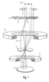
- a mask carrier 1 is shown schematically in FIG. 1, which is an object, namely to be imaged as a mask Structures 3 supports such that they in a focal plane a focusing magnetic lens 5 are arranged, i.e. have a distance from the magnetic lens that the Focal length of the magnetic lens corresponds.
- the lens 5 forms the object plane with the one to be imaged Pattern 3 goes to infinity, and it's another magnetic lens 7 provided, which is imaged by the lens 5 Images pattern on a substrate surface 9, which of the Lens 7 has a distance which corresponds to its focal length.
- a pinhole is between the two lenses 5 and 7 11 is provided, which is a distance from the lens 5 which corresponds to their focal length and which of the Lens 7 has a distance which is the focal length of the lens 7 corresponds.
- Particle beams 12, 13 which cover the mask enforce outside the structures to be imaged 3 the mask is essentially rectilinear such that it run through a so-called "crossover" point, which in the Center of the pinhole 11 is arranged so that this Rays are imaged on the substrate surface 9.
- the Structures 3 to be imaged are by means of an electron comparatively strong scattering material on the mask carrier 1 defines so that rays that are stronger on such scattering structure 3 meet from its original Direction of movement are deflected, as shown in Figure 1 for a beam 14 is shown. This can then be from the Lens 5 not on the crossover point in the pinhole 11 be deflected so that it is absorbed by the pinhole 11 and is therefore not imaged on the substrate 9.
- the entire mask can be illuminated optically at once, but it is also possible to just at any time to illuminate a subfield of the mask and this subfield moving across the mask surface.
- a partial field is indicated with central and marginal rays 12, which is centered on an optical axis 15 of the lenses 5 and 7 is arranged, and with 13 are central and marginal rays of a subfield indicated in the mask plane a distance M offset from the optical axis 15 is.
- mapping characteristics satisfying higher requirements especially for subfields that come from the optical axis are deflected, can not be reached.
- a lens arrangement for particle-optical imaging of one in an object area object to be mapped into an image area the lens arrangement a first and a second focusing lens device and a deflecting lens device includes.
- the object area and the Image area first one conveyed by the illustration have any shape, but in practice one Approximation of at least one of the surfaces to a flat shape are aimed to initially a simple design of the Allow object or / and the image area and then aberrations to reduce, among other things, the result that the object is not exactly in the intended object area or a substrate to be exposed is not exactly in the intended object area is arranged.
- the first focusing lens device provides a field which has a focusing effect on the imaging particles, so that at least a subfield of the object area into a subfield an intermediate image area of the lens arrangement is imaged.
- the second focusing lens device also focuses acting field ready, at least for mapping of the subfield of the intermediate image area into a subfield the image area.
- a deflecting lens device for providing a to the imaging particles deflecting field in the area the intermediate image area.
- the distracting field of Deflection lens device leads to a tilting of the intermediate image before it goes through the second focusing lens device is mapped onto the image surface. So it can with the deflection lens device aberrations that lead to a Tilting the image area relative to a target image area lead, be compensated. In particular, these are image errors, which are called image field curvature.
- the first or / and second focusing lens device a field ready, which one regarding a such a central ray of a beam of rays essentially Axially symmetrical magnetic and / or electrical Field includes.
- the first or / and second focusing lens device to achieve the focusing effect two or three with axial Have spaced field arrangements, the two field arrangements dipole and / or quadropole field arrangements or combinations thereof and together have the focusing effect.
- the two field arrangements dipole and / or quadropole field arrangements or combinations thereof and together have the focusing effect.
- Field arrangements that are not themselves non-rotationally symmetrical Generate fields, achieved a total lens effect that corresponds to that of a round lens.
- the deflecting field of the deflecting lens device steers this passing particle in essentially the same Direction down, which is why the field of the deflecting lens device in particular has no axial symmetry.
- the field of the deflecting lens device has mirror symmetry to a plane in which a central ray of a Beam of the imaging particles extends.
- the field of the deflecting lens device is a magnetic one or / and electric dipole field that is transverse to one Direction of propagation of the imaging particles is oriented.
- the field of the deflection lens device has on the imaging Particles thus have an effect equivalent to that of a wedge lens is comparable in light optics.
- the field of the deflection lens device is in a certain extending from the intermediate image area Area around the intermediate image area is effective, i.e. the area, into the object area through the first focusing lens device is mapped.
- the intermediate image surface has the property that particle beams, which is the object area from one place, however leave the intermediate image area at different angles in essentially a common place with also enforce different angles, with rays, that come from different locations of the object area, too enforce the intermediate image area in different places.
- the intermediate image area of the first focusing lens device differs from the diffraction surface of the first Focusing lens device, which is between the intermediate image plane and the first focusing lens device itself is.
- the diffraction surface has the property on them from rays that the object area from different Places, but leave at the same angle, in the same places, but at different angles is enforced.
- rays penetrate the object surface leave the diffraction surface at different angles also in different places.
- a diffraction surface assigned to the second focusing lens device is also between the intermediate image plane and the second focusing lens device arranged. In this second diffraction surface meet rays that cover the image surface meet at the same angle, on a common one Location, but at different angles.
- a diffraction surface is usually also referred to as a Fourier surface.
- an aperture is preferably provided, which absorbs rays that cover the object area under one Enforce an angle that exceeds a predetermined angle.
- the lens arrangement is preferably for imaging a Subfield of the object area provided on the image area, where the location of the subfield is also a subfield of the Object area is variably adjustable.
- a distance of the subfield from a given axis adjustable for example a central optical Axis of the first or / and second focusing lens device includes.
- the deflecting lens device is particularly suitable for effects of the field curvature, caused by aberrations of the first or / and second Focusing lens device are caused to compensate.
- a strength of the field of the deflection lens device is used preferably set so that it is proportional to the distance of the subfield from the given one Axis changes.
- the deflecting lens device leads to a tilting of the partial field depicted in the image area and can in particular be set such that the image area in the area of the subfield just shown one in roughly just in shape and thus one after the other in time all subfields of a flat object surface in im Essentially, a flat picture area can be mapped.
- the invention provides a method for the production of a component, it being preferred strongly miniaturized components such as micromechanical Structures or integrated circuits.
- a mask contains a circuit pattern, that of a single layer on an appropriate one Substrate, for example a silicon wafer Circuit corresponds.
- a target area English "Die"
- the substrate becomes the latter first with a radiation sensitive layer ("resist") covered.
- the radiation sensitive Layer exposed or exposed by the pattern of the mask by means of charged particles; for example electrons or Ions imaged on the radiation sensitive layer becomes.
- the radiation-sensitive layer is then developed and either the exposed or exposed or the unexposed or unexposed areas removed from the exposed layer.
- the structure of the radiation-sensitive layer then serves as Mask in, for example, an etching step, an ion implantation step, a material deposition step or the like.
- a photolithographic Step of the method a defined by a mask Pattern using the lens arrangement described above image on a particle sensitive substrate.
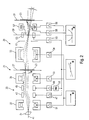
- An electron projection lithography arrangement shown in Figure 2 21 is used to define a mask 23 Structure on one with a radiation sensitive Layer semiconductor wafer 25 provided. This is the effective layer of the mask 23 in an object plane 27 a lens arrangement 29 arranged in its image plane 31 the radiation-sensitive layer of the wafer 25 is arranged is.
- the projection lithography arrangement 21 has the wafer 25 another lighting arrangement 33 for illuminating the mask 23 on.
- the lighting arrangement 33 comprises one in FIG. 2 Electron source, not shown, for illuminating a Beam shaping diaphragm 35, which is an illuminated subfield of the Mask 23 defined.
- the electron source, not shown Illuminated beam shaping diaphragm 35 is used for this into the object plane by means of two focusing lenses 37 and 39 27 of the lens arrangement 29 shown.
- the two focusing Lenses 37 and 39 are optical Axis 41 of the projection arrangement 21 is arranged symmetrically.
- the deflection units 43 and 45 have corresponding ones Drivers 47 and 49 on which one with the desired Deflection M of the subfield from the optical axis 41 proportional dependency can be controlled, although the control of the two drivers 47 and 49 with each the opposite sign takes place, for which purpose an inverter 50 is provided.
- the control of the focusing lenses 37 and 39 takes place via drivers 51 and 53 independently of the deflection M.
- the image of the illuminated subfield from the object level 27 of the lens arrangement 29 takes place in the image plane 31 thereof essentially by a focusing lens 55 and a further focusing lens 57.
- the focal lengths of the two focusing lenses 55 and 57 and their distances from the Object plane 27 and image plane 31 are coordinated with one another in such a way that that the mapping from object level 27 to the Image plane 31 is reduced by a factor of 1: 4.
- the focal lengths and distances are coordinated so that the object plane 27 through the focusing lens 55 initially in an intermediate image plane 59 is imaged, which is characterized by the Focusing lens 57 finally imaged in the image plane 31 becomes.
- a diffraction plane of the focusing lens 55 there is also one Pinhole 61 arranged, which absorbs the electrons a possibly more scattering structure of the mask 23 were scattered and therefore the radiation sensitive Layer on the wafer 25 should not reach, with which the desired mapping of the structures of the mask onto the Substrate is generated.
- a so-called dynamic focus coil 65 is provided, which is arranged within the focusing lens 57 is.
- the dynamic focus coil 65 is used for compensation a focus error and is triggered by a driver 58 driven in such a way that their field is essentially one quadratic dependence on the deflection of the subfield M changes.
- Such a compensation of a focus error depending on the deflection M of the subfield also done with the focusing lenses 55 and 57 itself. Indeed have these pole pieces and are therefore relative sluggish, so the compensation by the separate dynamic Focus coil 65 is possible more precisely.
- a deflection lens device 63 is provided between the intermediate image plane 59, what rays that pass through it, around deflects an adjustable angle ⁇ .
- the deflecting lens device 63 is controlled by means of a driver 60 in such a way that that the deflection angle ⁇ is essentially proportional for deflection M of the subfield from the optical axis 59 changes.
- turns of the deflecting lens device 63 are shown schematically in FIG. 3.
- this connection 3a shows the execution of turns as a toroid coil
- Figure 3b the execution as a saddle coil
- Figure 3c the Version as a composite saddle spool.
- the individual coil turns the deflecting lens device are on one or several ferrite rings 71 (see FIG. 4) wound up concentrically are arranged to the optical axis 41.
- the distribution of the individual turns in the circumferential direction of the ferrite ring 71 can be seen from FIG. 4.
- FIG. 4a shows windings that are used to generate a magnetic dipole field By directed in a Y direction
- FIG. 4b shows windings that are used to generate a dipole field B x orthogonal to this
- FIG. 4c shows the combination of the turns shown in FIGS. 4a and 4b on the ferrite ring 71.
- the focusing lenses 55 and 57 are in Figure 5 according to their optical analog as convex lenses shown, while the deflecting lens 59 according to their optical analog in Figure 5 symbolized as a wedge or prism is.
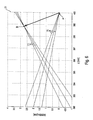
- FIG. 5 shows a lower edge ray bundle 73 of the subfield T and an upper edge ray bundle 75 of the same.
- the effect of the deflecting lens device 63 on the rays 73 and 75 is such that these are in the intermediate image plane 59 are each deflected by an angle ⁇ .
- Beam 75 which in the object plane 27 from the optical axis, i.e. an image height of 0 mm, united itself on the image plane 31 (intersection point A in FIG. 6).
- the beam 73 on the other hand, which is in the object plane 27 started at an image height of 12 mm, merges about 1 mm in front of the image plane 31 at an intersection B in FIG. 6.
- the lens arrangement 29 is only schematic as imaging system represented in the form of a box which an object surface 27 designed as a plane into an image surface 31 depicts.
- Figure 7a is the deflecting lens device 63 not in operation, and cause effects of the field curvature that the image surface is not, like the object surface 27, in a level 25 which, for example, the surface of a Wafers is arranged, but bulged out clearly from this is.
- a subfield T1 arranged centrally to the optical axis 41 is so by the lens assembly 29 on the curved Image area 31 shown that its center on the Wafer 25 is focused while its top edge is spaced x1 focused away from the surface of the wafer 25 is.
- FIG. 7b shows a first measure for correcting the curvature of the image field.
- the subfield T1 arranged centrally to the optical axis 41 is imaged by the lens arrangement 29 in the direction of the wafer 25, as was explained in connection with FIG. 7a.
- the partial field T1 is thus imaged in a partial field T1 'on an image area 31 1 , the center of which lies on the wafer 25.
- Edges of the image field T1 'thus have a focus error of x1, as was also the case in FIG. 7a.
- the dynamic focus coil 65 provides a magnetic focusing field in such a way that the object surface 27 is imaged on an image surface 31 2 , which is opposite the image surface 31 1 for the Subfield T1 is shifted such that a center of the depicted subfield T2 'intersects the wafer 25 or is focused on it.
- the image area is tilted into an image area 31 2 in such a way that the image area 31 2 is aligned symmetrically to the center of the depicted partial field T2 ′ on the wafer 25.
- a focusing error at the edges of the decentralized subfield T2 'shown is equal to the value x1 of the imaging error at the edges of the central subfield T1' shown.
- the selected tilting of the image surface leads to interaction with a corresponding focus correction, that the image area is special for a depicted subfield to a target image area, namely the wafer surface, is approximated.
- the Deflection lens device by a magnetic dipole field educated.
- an electrical one Dipole field or any other field to be provided Effect on an area around by the first focusing lens device 51 defined intermediate image plane to a Deflection of the rays or tilting of the intermediate image leads.
- the first and second focusing lens device is in the embodiment described above as one for optical axis 41 axisymmetric magnetic lens with pole pieces described. Alternatively, however, it is also possible the focusing effect through an electrostatic Generate field.
- the embodiment of the invention described above Lens assembly is in an electron projection lithography system used. However, it is also possible that Use lens arrangement in a system that is not works with electrons but with, for example, ions.
- the Lens assembly is also in a manufacturing process electronic components and for the manufacture of others miniaturized components can be used, the figure from the object area into the image area of exposure one particle-sensitive layer in a lithography step serves.
- the use of the lens arrangement is not limited to lithography steps, but always possible when an object surface with high precision is particle-optical in an image area of a desired shape is.
Landscapes
- Engineering & Computer Science (AREA)
- Chemical & Material Sciences (AREA)
- Nanotechnology (AREA)
- Physics & Mathematics (AREA)
- Crystallography & Structural Chemistry (AREA)
- Analytical Chemistry (AREA)
- General Physics & Mathematics (AREA)
- Manufacturing & Machinery (AREA)
- Condensed Matter Physics & Semiconductors (AREA)
- Mathematical Physics (AREA)
- Theoretical Computer Science (AREA)
- Optics & Photonics (AREA)
- Electron Beam Exposure (AREA)
- Exposure And Positioning Against Photoresist Photosensitive Materials (AREA)
Abstract
Description
- Figur 1
- eine Linsenanordnung gemäß dem Stand der Technik;
- Figur 2
- einen schematischen Aufbau einer erfindungs-gemäßen Linsenanordnung sowie einen schematischen Strahlengang hierdurch,
- Figur 3
- verschiedene Wicklungstypen einer in Figur 2 gezeigten Ablenklinseneinrichtung,
- Figur 4
- verschiedene Anordnungen von Stromleiterwindungen der in Figur 2 gezeigten Ablenklinseneinrichtung am Umfang eines Ferritrings,
- Figur 5
- eine weitere schematische Darstellung des Strahlengangs durch die in Figur 2 gezeigte Linsenanordnung und
- Figur 6
- eine vergrößerte Darstellung eines Teils der Figur 5 in der Nähe einer Bildfläche der Linsenanordnung, und
- Figur 7
- mehrere Darstellungen zur Erläuterung der Bildfehler reduzierenden Wirkung der erfindungsgemäßen Linsenanordnung.
Claims (13)
- Linsenanordnung zur teilchenoptischen Abbildung eines in einer Objektfläche (27) anordenbaren abzubildenden Objekts (23) in eine Bildfläche (31), umfassend:eine erste Fokussierlinseneinrichtung (55) zur Bereitstellung eines auf die abbildenden Teilchen fokussierend wirkenden Feldes zur Abbildung des Objekts (23) von der Objektfläche (27) in eine Zwischenbildfläche (59),eine zweite Fokussierlinseneinrichtung (57) zur Bereitstellung eines weiteren auf die abbildenden Teilchen fokussierend wirkenden Feldes zur Abbildung des in die Zwischenbildfläche (59) abgebildeten Objekts (23) in die Bildfläche (31), undeine Ablenklinseneinrichtung (63) zur Bereitstellung eines auf die abbildenden Teilchen ablenkend wirkenden Feldes in einem Bereich der Zwischenbildfläche (59).
- Linsenanordnung nach Anspruch 1, wobei das Feld der ersten oder/und zweiten Fokussierlinseneinrichtung (55) ein bezüglich einem Zentralstrahl eines Strahlenbündels (73) der abbildenden Teilchen im Wesentlichen achssymmetrisch ausgebildetes magnetisches oder/und elektrisches Feld umfasst.
- Linsenanordnung nach Anspruch 1, wobei das Feld der ersten oder/und zweiten Fokussierlinseneinrichtung zwei bezüglich einem Zentralstrahl eines Strahlenbündels der abbildenden Teilchen mit axialem Abstand voneinander angeordnete magnetische oder/und elektrische Dipoloder/und Quadrupol-Feldanordnungen umfasst.
- Linsenanordnung nach einem der Ansprüche 1 bis 3, wobei das Feld der Ablenklinseneinrichtung (63) ein bezüglich einer gemeinsam mit einem Zentralstrahl eines Strahlenbündels der abbildenden Teilchen sich erstreckenden Ebene im Wesentlichen spiegelsymetrisch ausgebildetes magnetisches Feld umfasst.
- Linsenanordnung nach einem der Ansprüche 1 bis 4, wobei das Feld der Ablenklinseneinrichtung (63) ein quer zu einem Zentralstrahl eines Strahlenbündels der abbildenden Teilchen ausgerichtetes magnetisches oder/und elektrisches Dipolfeld umfasst.
- Linsenanordnung nach einem der Ansprüche 1 bis 5, wobei in einer Beugungsebene (61) der ersten Fokussierlinseneinrichtung (55) oder/und der zweiten Fokussierlinseneinrichtung (57) eine Lochblende (61) vorgesehen ist.
- Linsenanordnung nach einem der Ansprüche 1 bis 6, ferner umfassend eine erste Ansteuereinrichtung für die Ablenklinseneinrichtung (63) zur Einstellung einer Stärke von deren ablenkend wirkenden Feld und eine zweite Ansteuereinrichtung für die erste Fokussierlinseneinrichtung (55) oder/und die zweite Fokussierlinseneinrichtung (57) zur Einstellung einer Stärke von deren fokussierend wirkenden Feldern, wobei die erste Ansteuereinrichtung die Stärke des Feldes der Ablenklinseneinrichtung (63) mit einer im Wesentlichen proportionalen Abhängigkeit von einer externen Grösse (M) ändert und die zweite Ansteuereinrichtung die Stärke des Feldes der ersten bzw. zweiten Fokussierlinseneinrichtung (55), (57) mit einer im wesentlichen quadratischen Abhängigkeit von der externen Grösse (M) ändert.
- Linsenanordnung nach Anspruch 7, wobei die Linsenanordnung (29) zur Abbildung eines von einer optischen Achse (41) der Linsenanordnung (29) einen variablen Abstand (M) aufweisenden Teilfeldes (T) der Objektfläche (27) auf die Bildfläche (31) vorgesehen ist und wobei die externe Grösse den Abstand (M) des Teilfeldes (T) von der optischen Achse (41) umfasst.
- Linsenanordnung nach Anspruch 8, wobei das Feld der Ablenklinseneinrichtung (63) paarweise verschiedene Strahlen der das Teilfeld (T) abbildenden Teilchenstrahlen (73, 75) um im Wesentlichen gleiche Winkel α ablenkt.
- Linsenanordnung nach Anspruch 8 oder 9, ferner umfassend eine Beleuchtungseinrichtung (35, 37, 39, 43, 45) zur Beleuchtung lediglich des Teilfeldes (T) der Objektfläche (27) und eine dritte Ansteuervorrichtung (47, 49) für die Beleuchtungseinrichtung, mittels der die Beleuchtungseinrichtung ansteuerbar ist, um den Abstand (M) des beleuchteten Teilfeldes (T) von der optischen Achse (41) zu ändern.
- Linsenanordnung nach einem der Ansprüche 8 bis 10, wobei Bildfläche (31) und die Objektfläche (27) jeweils eine vorbestimmte Sollgestalt aufweisen, wobei die zweite Ansteuervorrichtung die Stärke des Ablenkfeldes der ersten bzw. zweiten Fokussiereinrichtung derart ändert, dass ein zentraler Bereich des Teilfeldes (T) im Wesentlichen scharf auf die Bildfläche abgebildet wird, und wobei die erste Ansteuervorrichtung die Stärke des Ablenkfeldes der Ablenklinseneinrichtung derart ändert, dass auch Randbereiche des Teilfeldes im Wesentlichen scharf auf die Bildfläche abgebildet werden.
- Linsenanordnung nach Anspruch 11, wobei die Gestalt der Objektfläche eine Ebene ist.
- Verfahren zur Herstellung eines Bauelements, umfassend wenigstens einen photolithographischen Schritt, wobei der photolithographische Schritt das Übertragen eines durch eine Maske (23) definierten Musters auf ein teilchenempfindliches Substrat (25) mittels der Linsenanordnung (29) nach einem der Ansprüche 1 bis 12 umfasst, wobei die Maske (23) in der Objektfläche (27) und das Substrat (25) in der Bildfläche (31) angeordnet sind.
Applications Claiming Priority (2)
| Application Number | Priority Date | Filing Date | Title |
|---|---|---|---|
| DE10109965 | 2001-03-01 | ||
| DE10109965A DE10109965A1 (de) | 2001-03-01 | 2001-03-01 | Teilchenoptische Linsenanordnung und Verfahren unter Einsatz einer solchen Linsenanordnung |
Publications (2)
| Publication Number | Publication Date |
|---|---|
| EP1239510A1 true EP1239510A1 (de) | 2002-09-11 |
| EP1239510B1 EP1239510B1 (de) | 2007-08-01 |
Family
ID=7675993
Family Applications (1)
| Application Number | Title | Priority Date | Filing Date |
|---|---|---|---|
| EP02004543A Expired - Lifetime EP1239510B1 (de) | 2001-03-01 | 2002-02-27 | Teilchenoptische Linsenanordnung und Verfahren unter Einsatz einer solchen Linsenanordnung |
Country Status (6)
| Country | Link |
|---|---|
| US (1) | US6777166B2 (de) |
| EP (1) | EP1239510B1 (de) |
| JP (1) | JP2002343714A (de) |
| KR (1) | KR100854695B1 (de) |
| DE (2) | DE10109965A1 (de) |
| TW (1) | TW556245B (de) |
Cited By (1)
| Publication number | Priority date | Publication date | Assignee | Title |
|---|---|---|---|---|
| CN103257511A (zh) * | 2013-04-27 | 2013-08-21 | 宁波舜宇光电信息有限公司 | 一种基于镜头场曲的自动对焦方法 |
Families Citing this family (11)
| Publication number | Priority date | Publication date | Assignee | Title |
|---|---|---|---|---|
| JP3968334B2 (ja) * | 2002-09-11 | 2007-08-29 | 株式会社日立ハイテクノロジーズ | 荷電粒子線装置及び荷電粒子線照射方法 |
| JP4620981B2 (ja) * | 2004-08-10 | 2011-01-26 | 株式会社日立ハイテクノロジーズ | 荷電粒子ビーム装置 |
| KR100590574B1 (ko) * | 2004-12-21 | 2006-06-19 | 삼성전자주식회사 | 전자기장 포커싱 장치 및 이를 채용한 전자빔 리소그라피시스템 |
| JP5420678B2 (ja) * | 2009-12-11 | 2014-02-19 | 株式会社日立製作所 | 電子線バイプリズム装置および電子線装置 |
| JP2011238387A (ja) * | 2010-05-07 | 2011-11-24 | Jeol Ltd | エミッタアレイを用いた電子プローブ装置 |
| JP6002428B2 (ja) * | 2012-04-24 | 2016-10-05 | 株式会社日立ハイテクノロジーズ | 荷電粒子線装置 |
| US9752992B2 (en) | 2014-03-25 | 2017-09-05 | Kla-Tencor Corporation | Variable image field curvature for object inspection |
| JP6161571B2 (ja) * | 2014-05-26 | 2017-07-12 | 住友重機械イオンテクノロジー株式会社 | イオン注入装置 |
| CN109767971B (zh) * | 2019-03-08 | 2024-08-13 | 昆山禾信质谱技术有限公司 | 二维离子束偏转装置 |
| JP7208212B2 (ja) * | 2020-11-30 | 2023-01-18 | 日本電子株式会社 | 透過電子顕微鏡および光学系の調整方法 |
| WO2022192207A1 (en) * | 2021-03-11 | 2022-09-15 | University Of Florida Research Foundation, Incorporated | Aberration corrected optical assembly |
Citations (4)
| Publication number | Priority date | Publication date | Assignee | Title |
|---|---|---|---|---|
| US5747819A (en) * | 1995-11-01 | 1998-05-05 | Nikon Corporation | Charged particle beam transfer device exhibiting low aberration |
| JPH1125896A (ja) * | 1997-06-30 | 1999-01-29 | Nikon Corp | 電子光学系 |
| US5973333A (en) * | 1997-03-25 | 1999-10-26 | Nikon Corporation | Charged-particle-beam pattern-transfer apparatus and methods |
| US6060711A (en) * | 1997-01-27 | 2000-05-09 | Nikon Corporation | Charged-particle optical systems and pattern transfer apparatus comprising same |
Family Cites Families (46)
| Publication number | Priority date | Publication date | Assignee | Title |
|---|---|---|---|---|
| US4243866A (en) * | 1979-01-11 | 1981-01-06 | International Business Machines Corporation | Method and apparatus for forming a variable size electron beam |
| US4376249A (en) | 1980-11-06 | 1983-03-08 | International Business Machines Corporation | Variable axis electron beam projection system |
| JPS57206173A (en) | 1981-06-15 | 1982-12-17 | Nippon Telegr & Teleph Corp <Ntt> | Focusing deflecting device for charged corpuscule beam |
| US4544846A (en) | 1983-06-28 | 1985-10-01 | International Business Machines Corporation | Variable axis immersion lens electron beam projection system |
| NL8602177A (nl) | 1986-08-27 | 1988-03-16 | Philips Nv | Electronen detectie met energie discriminatie. |
| US4929838A (en) | 1988-02-16 | 1990-05-29 | Fujitsu Limited | Magnetic object lens for an electron beam exposure apparatus which processes a wafer carried on a continuously moving stage |
| NL8801208A (nl) | 1988-05-09 | 1989-12-01 | Philips Nv | Geladen deeltjes bundel apparaat. |
| US4945246A (en) | 1989-03-24 | 1990-07-31 | International Business Machines Corporation | Tri-deflection electron beam system |
| US5258246A (en) | 1989-08-07 | 1993-11-02 | At&T Bell Laboratories | Device manufacture involving lithographic processing |
| DE3929774A1 (de) * | 1989-09-02 | 1991-03-07 | Hans W P Dipl Phys Dr Koops | Korpuskularstrahloptisches geraet mit kompensierten beleuchtungs- und abbildungsfehlern zur korpuskelbestrahlung eines praeparates in form eines flaechenmusters |
| US5285074A (en) | 1992-06-03 | 1994-02-08 | International Business Machines Corporation | Dynamic compensation of non-linear electron beam landing angle in variable axis lenses |
| US5389858A (en) | 1992-07-16 | 1995-02-14 | International Business Machines Corporation | Variable axis stigmator |
| US5382498A (en) | 1992-12-16 | 1995-01-17 | At&T Corp. | Processes for electron lithography |
| US5523580A (en) | 1993-12-23 | 1996-06-04 | International Business Machines Corporation | Reticle having a number of subfields |
| US5466904A (en) | 1993-12-23 | 1995-11-14 | International Business Machines Corporation | Electron beam lithography system |
| US5674413A (en) | 1993-12-23 | 1997-10-07 | International Business Machines Corporation | Scattering reticle for electron beam systems |
| US5849437A (en) * | 1994-03-25 | 1998-12-15 | Fujitsu Limited | Electron beam exposure mask and method of manufacturing the same and electron beam exposure method |
| US5633507A (en) | 1995-09-19 | 1997-05-27 | International Business Machines Corporation | Electron beam lithography system with low brightness |
| US5770863A (en) | 1995-10-24 | 1998-06-23 | Nikon Corporation | Charged particle beam projection apparatus |
| EP0794552B1 (de) * | 1996-03-04 | 2007-11-14 | Canon Kabushiki Kaisha | Elektronenstrahl-Belichtungsgerät, Belichtungsverfahren und Verfahren zur Erzeugung eines Objekts |
| JP3455006B2 (ja) * | 1996-03-25 | 2003-10-06 | 株式会社東芝 | 荷電粒子ビーム装置 |
| US6051839A (en) | 1996-06-07 | 2000-04-18 | Arch Development Corporation | Magnetic lens apparatus for use in high-resolution scanning electron microscopes and lithographic processes |
| US5635719A (en) | 1996-07-23 | 1997-06-03 | International Business Machines Corporation | Variable curvilinear axis deflection means for particle optical lenses |
| JPH1040848A (ja) | 1996-07-25 | 1998-02-13 | Nikon Corp | 荷電粒子線装置 |
| JPH1097979A (ja) | 1996-09-25 | 1998-04-14 | Nikon Corp | 縮小投影装置 |
| US5825043A (en) | 1996-10-07 | 1998-10-20 | Nikon Precision Inc. | Focusing and tilting adjustment system for lithography aligner, manufacturing apparatus or inspection apparatus |
| US5747814A (en) | 1996-12-06 | 1998-05-05 | International Business Machines Corporation | Method for centering a lens in a charged-particle system |
| US5757010A (en) | 1996-12-18 | 1998-05-26 | International Business Machines Corporation | Curvilinear variable axis lens correction with centered dipoles |
| US5708274A (en) | 1996-12-18 | 1998-01-13 | International Business Machines Corporation | Curvilinear variable axis lens correction with crossed coils |
| US5793048A (en) | 1996-12-18 | 1998-08-11 | International Business Machines Corporation | Curvilinear variable axis lens correction with shifted dipoles |
| JPH10294255A (ja) | 1997-04-17 | 1998-11-04 | Canon Inc | 電子ビーム照明装置、および該電子ビーム照明装置を備えた露光装置 |
| US6064071A (en) | 1997-04-23 | 2000-05-16 | Nikon Corporation | Charged-particle-beam optical systems |
| JPH10303117A (ja) | 1997-04-30 | 1998-11-13 | Nikon Corp | 電子線光学系 |
| JPH10303118A (ja) | 1997-04-30 | 1998-11-13 | Nikon Corp | 電子線投影光学系 |
| JPH1131470A (ja) | 1997-07-08 | 1999-02-02 | Nikon Corp | 電子光学系 |
| JPH1173900A (ja) | 1997-08-28 | 1999-03-16 | Nikon Corp | 荷電粒子線光学系 |
| US6124596A (en) * | 1997-08-28 | 2000-09-26 | Nikon Corporation | Charged-particle-beam projection apparatus and transfer methods |
| DE19738070A1 (de) | 1997-09-01 | 1999-03-04 | Leo Elektronenmikroskopie Gmbh | Energiefilter, insbesondere für ein Elektronenmikroskop |
| US6066855A (en) | 1997-10-07 | 2000-05-23 | Nikon Corporation | Charged-particle-beam optical system exhibiting aberration correction |
| US6069684A (en) | 1998-02-04 | 2000-05-30 | International Business Machines Corporation | Electron beam projection lithography system (EBPS) |
| DE19855629A1 (de) | 1998-12-02 | 2000-06-08 | Leo Elektronenmikroskopie Gmbh | Teilchenoptische Anordnung und Verfahren zur teilchenoptischen Erzeugung von Mikrostrukturen |
| EP0969326B1 (de) | 1998-07-01 | 2012-10-17 | ASML Netherlands B.V. | Lithographischer Apparat |
| US6023067A (en) | 1998-08-22 | 2000-02-08 | Nikon Corporation | Blanking system for electron beam projection system |
| US6005250A (en) | 1998-08-22 | 1999-12-21 | Nikon Corporation | Illumination deflection system for E-beam projection |
| US6280906B1 (en) * | 1998-12-22 | 2001-08-28 | U.S. Philips Corporation | Method of imaging a mask pattern on a substrate by means of EUV radiation, and apparatus and mask for performing the method |
| US6355384B1 (en) * | 2000-03-06 | 2002-03-12 | Motorola, Inc. | Mask, its method of formation, and a semiconductor device made thereby |
-
2001
- 2001-03-01 DE DE10109965A patent/DE10109965A1/de not_active Withdrawn
-
2002
- 2002-02-22 TW TW091103208A patent/TW556245B/zh not_active IP Right Cessation
- 2002-02-27 DE DE50210577T patent/DE50210577D1/de not_active Expired - Fee Related
- 2002-02-27 EP EP02004543A patent/EP1239510B1/de not_active Expired - Lifetime
- 2002-02-27 KR KR1020020010625A patent/KR100854695B1/ko not_active Expired - Fee Related
- 2002-02-28 JP JP2002054501A patent/JP2002343714A/ja active Pending
- 2002-03-01 US US10/087,601 patent/US6777166B2/en not_active Expired - Lifetime
Patent Citations (4)
| Publication number | Priority date | Publication date | Assignee | Title |
|---|---|---|---|---|
| US5747819A (en) * | 1995-11-01 | 1998-05-05 | Nikon Corporation | Charged particle beam transfer device exhibiting low aberration |
| US6060711A (en) * | 1997-01-27 | 2000-05-09 | Nikon Corporation | Charged-particle optical systems and pattern transfer apparatus comprising same |
| US5973333A (en) * | 1997-03-25 | 1999-10-26 | Nikon Corporation | Charged-particle-beam pattern-transfer apparatus and methods |
| JPH1125896A (ja) * | 1997-06-30 | 1999-01-29 | Nikon Corp | 電子光学系 |
Non-Patent Citations (1)
| Title |
|---|
| PATENT ABSTRACTS OF JAPAN vol. 1999, no. 04 30 April 1999 (1999-04-30) * |
Cited By (2)
| Publication number | Priority date | Publication date | Assignee | Title |
|---|---|---|---|---|
| CN103257511A (zh) * | 2013-04-27 | 2013-08-21 | 宁波舜宇光电信息有限公司 | 一种基于镜头场曲的自动对焦方法 |
| CN103257511B (zh) * | 2013-04-27 | 2016-01-20 | 宁波舜宇光电信息有限公司 | 一种基于镜头场曲的自动对焦方法 |
Also Published As
| Publication number | Publication date |
|---|---|
| US6777166B2 (en) | 2004-08-17 |
| DE50210577D1 (de) | 2007-09-13 |
| KR100854695B1 (ko) | 2008-08-27 |
| JP2002343714A (ja) | 2002-11-29 |
| TW556245B (en) | 2003-10-01 |
| US20020126366A1 (en) | 2002-09-12 |
| DE10109965A1 (de) | 2002-09-12 |
| KR20020070841A (ko) | 2002-09-11 |
| EP1239510B1 (de) | 2007-08-01 |
Similar Documents
| Publication | Publication Date | Title |
|---|---|---|
| DE69822139T2 (de) | Korrekturvorrichtung zur linsenfehlerkorrektur in ladungsträger-optischen geräten | |
| DE69738276T2 (de) | Elektronenstrahl-Belichtungsgerät, Belichtungsverfahren und Verfahren zur Erzeugung eines Objekts | |
| DE10044199B4 (de) | Ablenkanordnung und Projektionssystem für geladene Teilchen | |
| DE102008035297B4 (de) | Aberrationskorrektureinrichtung für Ladungsteilchenstrahlen in einem optischen System einer Ladungsteilchenstrahlvorrichtung und Ladungsteilchenstrahlvorrichtung mit der Aberrationskorrektureinrichtung | |
| DE69733408T2 (de) | Korrigiervorrichtung zur korrektur chromatischer fehler in einem partikel-optischen gerät | |
| EP1239510B1 (de) | Teilchenoptische Linsenanordnung und Verfahren unter Einsatz einer solchen Linsenanordnung | |
| DE69023030T2 (de) | Dreifache Ablenkung für eine Elektronenstrahlanordnung. | |
| DE8634545U1 (de) | Korpuskularstrahlgerät zur fehlerarmen Abbildung linienförmiger Objekte | |
| DE69920182T2 (de) | Korpuskularstrahloptisches gerät mit auger-elektronendetektion | |
| DE2727733C2 (de) | Elektronenstrahllithographieanordnung | |
| DE3852097T2 (de) | Telezentrische Ablenkung auf Sekundärfelder mittels einer Immersionslinse mit variabler Achse. | |
| DE102009054540A1 (de) | Beleuchtungsoptik für die EUV-Mikrolithographie | |
| EP1172837B1 (de) | Verfahren zur Elektronenstrahl-Lithographie und elektronen-optisches Lithographiesystem | |
| DE10028327A1 (de) | Vorrichtung und Verfahren für bildformende Strahlen aus geladenen Teilchen und Bestrahlungsvorrichtung mit Strahlen aus geladenen Teilchen | |
| EP0106154B1 (de) | Varioformstrahl-Ablenkobjektiv für Neutralteilchen und Verfahren zu seinem Betrieb | |
| EP0231164B1 (de) | Einrichtung für Ionenprojektionsgeräte | |
| DE69202782T2 (de) | Feldemissions-Elektronenkanone geringer Aberration. | |
| EP0564438A1 (de) | Teilchen-, insbes. ionenoptisches Abbildungssystem | |
| EP0739531B1 (de) | Teilchenoptisches abbildungssystem | |
| DE102004019834B4 (de) | Korrekturlinsen-System für ein Partikelstrahl-Projektionsgerät | |
| EP1410416B1 (de) | Schlitzlinsenanordnung fur teilchenstrahlen | |
| DE102004019835B4 (de) | Beleuchtungskondensor für ein Partikeloptik-Projektionssystem | |
| DE69913100T2 (de) | Projektionslithographie mittels ladungsträgern | |
| DE69913313T2 (de) | Quadrupol-Vorrichtung für Projektionslithographie mittels geladener Teilchen | |
| DE10255032A1 (de) | Verringerung von Aberrationen, die in einem Rasterelektronenmikroskop oder Ähnlichem durch ein Wien-Filter erzeugt werden |
Legal Events
| Date | Code | Title | Description |
|---|---|---|---|
| PUAI | Public reference made under article 153(3) epc to a published international application that has entered the european phase |
Free format text: ORIGINAL CODE: 0009012 |
|
| AK | Designated contracting states |
Kind code of ref document: A1 Designated state(s): AT BE CH CY DE DK ES FI FR GB GR IE IT LI LU MC NL PT SE TR |
|
| AX | Request for extension of the european patent |
Free format text: AL;LT;LV;MK;RO;SI |
|
| 17P | Request for examination filed |
Effective date: 20030218 |
|
| AKX | Designation fees paid |
Designated state(s): DE GB NL |
|
| RAP1 | Party data changed (applicant data changed or rights of an application transferred) |
Owner name: CARL ZEISS SMT AG |
|
| 17Q | First examination report despatched |
Effective date: 20050414 |
|
| 17Q | First examination report despatched |
Effective date: 20050414 |
|
| GRAP | Despatch of communication of intention to grant a patent |
Free format text: ORIGINAL CODE: EPIDOSNIGR1 |
|
| RAP1 | Party data changed (applicant data changed or rights of an application transferred) |
Owner name: CARL ZEISS SMT AG |
|
| GRAS | Grant fee paid |
Free format text: ORIGINAL CODE: EPIDOSNIGR3 |
|
| GRAA | (expected) grant |
Free format text: ORIGINAL CODE: 0009210 |
|
| AK | Designated contracting states |
Kind code of ref document: B1 Designated state(s): DE GB NL |
|
| REG | Reference to a national code |
Ref country code: GB Ref legal event code: FG4D Free format text: NOT ENGLISH |
|
| RAP2 | Party data changed (patent owner data changed or rights of a patent transferred) |
Owner name: CARL ZEISS SMT AG |
|
| REF | Corresponds to: |
Ref document number: 50210577 Country of ref document: DE Date of ref document: 20070913 Kind code of ref document: P |
|
| GBT | Gb: translation of ep patent filed (gb section 77(6)(a)/1977) |
Effective date: 20071001 |
|
| NLT2 | Nl: modifications (of names), taken from the european patent patent bulletin |
Owner name: CARL ZEISS SMT AG Effective date: 20070905 |
|
| PLBE | No opposition filed within time limit |
Free format text: ORIGINAL CODE: 0009261 |
|
| STAA | Information on the status of an ep patent application or granted ep patent |
Free format text: STATUS: NO OPPOSITION FILED WITHIN TIME LIMIT |
|
| 26N | No opposition filed |
Effective date: 20080506 |
|
| PGFP | Annual fee paid to national office [announced via postgrant information from national office to epo] |
Ref country code: DE Payment date: 20090219 Year of fee payment: 8 Ref country code: NL Payment date: 20090217 Year of fee payment: 8 |
|
| PGFP | Annual fee paid to national office [announced via postgrant information from national office to epo] |
Ref country code: GB Payment date: 20090219 Year of fee payment: 8 |
|
| REG | Reference to a national code |
Ref country code: NL Ref legal event code: V1 Effective date: 20100901 |
|
| GBPC | Gb: european patent ceased through non-payment of renewal fee |
Effective date: 20100227 |
|
| PG25 | Lapsed in a contracting state [announced via postgrant information from national office to epo] |
Ref country code: NL Free format text: LAPSE BECAUSE OF NON-PAYMENT OF DUE FEES Effective date: 20100901 |
|
| PG25 | Lapsed in a contracting state [announced via postgrant information from national office to epo] |
Ref country code: DE Free format text: LAPSE BECAUSE OF NON-PAYMENT OF DUE FEES Effective date: 20100901 |
|
| PG25 | Lapsed in a contracting state [announced via postgrant information from national office to epo] |
Ref country code: GB Free format text: LAPSE BECAUSE OF NON-PAYMENT OF DUE FEES Effective date: 20100227 |