EP1225622B1 - Halbleiteranordnung - Google Patents
HalbleiteranordnungInfo
- Publication number
- EP1225622B1 EP1225622B1 EP02000298A EP02000298A EP1225622B1 EP 1225622 B1 EP1225622 B1 EP 1225622B1 EP 02000298 A EP02000298 A EP 02000298A EP 02000298 A EP02000298 A EP 02000298A EP 1225622 B1 EP1225622 B1 EP 1225622B1
- Authority
- EP
- European Patent Office
- Prior art keywords
- impurity doped
- doped layer
- layer
- recited
- source
- Prior art date
- Legal status (The legal status is an assumption and is not a legal conclusion. Google has not performed a legal analysis and makes no representation as to the accuracy of the status listed.)
- Expired - Lifetime
Links
- 239000004065 semiconductor Substances 0.000 title claims description 28
- 239000012535 impurity Substances 0.000 claims description 90
- 239000000758 substrate Substances 0.000 claims description 39
- 238000009792 diffusion process Methods 0.000 claims description 23
- 230000015572 biosynthetic process Effects 0.000 claims description 17
- 229910052751 metal Inorganic materials 0.000 claims description 10
- 239000002184 metal Substances 0.000 claims description 10
- 229910021420 polycrystalline silicon Inorganic materials 0.000 claims description 5
- 229920005591 polysilicon Polymers 0.000 claims description 4
- 239000010410 layer Substances 0.000 description 189
- 108091006146 Channels Proteins 0.000 description 58
- 238000000034 method Methods 0.000 description 41
- 239000010408 film Substances 0.000 description 36
- 229910052710 silicon Inorganic materials 0.000 description 35
- 239000010703 silicon Substances 0.000 description 35
- 238000005468 ion implantation Methods 0.000 description 34
- XUIMIQQOPSSXEZ-UHFFFAOYSA-N Silicon Chemical compound [Si] XUIMIQQOPSSXEZ-UHFFFAOYSA-N 0.000 description 33
- 230000000694 effects Effects 0.000 description 20
- 230000008569 process Effects 0.000 description 20
- 238000004519 manufacturing process Methods 0.000 description 17
- 238000002955 isolation Methods 0.000 description 15
- 230000007423 decrease Effects 0.000 description 11
- 230000010354 integration Effects 0.000 description 8
- 230000008901 benefit Effects 0.000 description 7
- 238000010586 diagram Methods 0.000 description 7
- 238000009826 distribution Methods 0.000 description 7
- 230000005684 electric field Effects 0.000 description 6
- 229910052581 Si3N4 Inorganic materials 0.000 description 5
- 125000001475 halogen functional group Chemical group 0.000 description 5
- HQVNEWCFYHHQES-UHFFFAOYSA-N silicon nitride Chemical compound N12[Si]34N5[Si]62N3[Si]51N64 HQVNEWCFYHHQES-UHFFFAOYSA-N 0.000 description 5
- ZOXJGFHDIHLPTG-UHFFFAOYSA-N Boron Chemical compound [B] ZOXJGFHDIHLPTG-UHFFFAOYSA-N 0.000 description 4
- 230000001133 acceleration Effects 0.000 description 4
- 229910052796 boron Inorganic materials 0.000 description 4
- 230000036039 immunity Effects 0.000 description 4
- 239000012212 insulator Substances 0.000 description 4
- 238000005457 optimization Methods 0.000 description 4
- 108010075750 P-Type Calcium Channels Proteins 0.000 description 3
- 238000013459 approach Methods 0.000 description 3
- 150000002500 ions Chemical class 0.000 description 3
- 238000003475 lamination Methods 0.000 description 3
- 230000003071 parasitic effect Effects 0.000 description 3
- 238000001020 plasma etching Methods 0.000 description 3
- 230000001629 suppression Effects 0.000 description 3
- 229910000577 Silicon-germanium Inorganic materials 0.000 description 2
- ATJFFYVFTNAWJD-UHFFFAOYSA-N Tin Chemical compound [Sn] ATJFFYVFTNAWJD-UHFFFAOYSA-N 0.000 description 2
- 229910052785 arsenic Inorganic materials 0.000 description 2
- RQNWIZPPADIBDY-UHFFFAOYSA-N arsenic atom Chemical compound [As] RQNWIZPPADIBDY-UHFFFAOYSA-N 0.000 description 2
- 210000000746 body region Anatomy 0.000 description 2
- 230000005669 field effect Effects 0.000 description 2
- 230000006872 improvement Effects 0.000 description 2
- 239000011229 interlayer Substances 0.000 description 2
- 239000000463 material Substances 0.000 description 2
- 239000011295 pitch Substances 0.000 description 2
- 230000009467 reduction Effects 0.000 description 2
- 150000003376 silicon Chemical class 0.000 description 2
- 230000004913 activation Effects 0.000 description 1
- 230000002411 adverse Effects 0.000 description 1
- 229910045601 alloy Inorganic materials 0.000 description 1
- 239000000956 alloy Substances 0.000 description 1
- 230000015556 catabolic process Effects 0.000 description 1
- 230000000295 complement effect Effects 0.000 description 1
- 238000006731 degradation reaction Methods 0.000 description 1
- 238000013461 design Methods 0.000 description 1
- 238000007599 discharging Methods 0.000 description 1
- 238000002513 implantation Methods 0.000 description 1
- 238000002347 injection Methods 0.000 description 1
- 239000007924 injection Substances 0.000 description 1
- 230000007246 mechanism Effects 0.000 description 1
- 229910044991 metal oxide Inorganic materials 0.000 description 1
- 150000004706 metal oxides Chemical class 0.000 description 1
- 239000000203 mixture Substances 0.000 description 1
- 238000012545 processing Methods 0.000 description 1
- 230000007261 regionalization Effects 0.000 description 1
- 238000012827 research and development Methods 0.000 description 1
- 238000004088 simulation Methods 0.000 description 1
- 230000003068 static effect Effects 0.000 description 1
- 238000003860 storage Methods 0.000 description 1
- 239000010409 thin film Substances 0.000 description 1
- WFKWXMTUELFFGS-UHFFFAOYSA-N tungsten Chemical compound [W] WFKWXMTUELFFGS-UHFFFAOYSA-N 0.000 description 1
- 229910052721 tungsten Inorganic materials 0.000 description 1
- 239000010937 tungsten Substances 0.000 description 1
Images


Classifications
-
- H—ELECTRICITY
- H10—SEMICONDUCTOR DEVICES; ELECTRIC SOLID-STATE DEVICES NOT OTHERWISE PROVIDED FOR
- H10D—INORGANIC ELECTRIC SEMICONDUCTOR DEVICES
- H10D30/00—Field-effect transistors [FET]
- H10D30/60—Insulated-gate field-effect transistors [IGFET]
-
- H—ELECTRICITY
- H10—SEMICONDUCTOR DEVICES; ELECTRIC SOLID-STATE DEVICES NOT OTHERWISE PROVIDED FOR
- H10D—INORGANIC ELECTRIC SEMICONDUCTOR DEVICES
- H10D30/00—Field-effect transistors [FET]
- H10D30/01—Manufacture or treatment
- H10D30/021—Manufacture or treatment of FETs having insulated gates [IGFET]
- H10D30/027—Manufacture or treatment of FETs having insulated gates [IGFET] of lateral single-gate IGFETs
- H10D30/0275—Manufacture or treatment of FETs having insulated gates [IGFET] of lateral single-gate IGFETs forming single crystalline semiconductor source or drain regions resulting in recessed gates, e.g. forming raised source or drain regions
-
- H—ELECTRICITY
- H10—SEMICONDUCTOR DEVICES; ELECTRIC SOLID-STATE DEVICES NOT OTHERWISE PROVIDED FOR
- H10D—INORGANIC ELECTRIC SEMICONDUCTOR DEVICES
- H10D30/00—Field-effect transistors [FET]
- H10D30/60—Insulated-gate field-effect transistors [IGFET]
- H10D30/601—Insulated-gate field-effect transistors [IGFET] having lightly-doped drain or source extensions, e.g. LDD IGFETs or DDD IGFETs
- H10D30/608—Insulated-gate field-effect transistors [IGFET] having lightly-doped drain or source extensions, e.g. LDD IGFETs or DDD IGFETs having non-planar bodies, e.g. having recessed gate electrodes
-
- H—ELECTRICITY
- H10—SEMICONDUCTOR DEVICES; ELECTRIC SOLID-STATE DEVICES NOT OTHERWISE PROVIDED FOR
- H10D—INORGANIC ELECTRIC SEMICONDUCTOR DEVICES
- H10D62/00—Semiconductor bodies, or regions thereof, of devices having potential barriers
- H10D62/10—Shapes, relative sizes or dispositions of the regions of the semiconductor bodies; Shapes of the semiconductor bodies
- H10D62/17—Semiconductor regions connected to electrodes not carrying current to be rectified, amplified or switched, e.g. channel regions
- H10D62/351—Substrate regions of field-effect devices
- H10D62/357—Substrate regions of field-effect devices of FETs
- H10D62/364—Substrate regions of field-effect devices of FETs of IGFETs
- H10D62/371—Inactive supplementary semiconductor regions, e.g. for preventing punch-through, improving capacity effect or leakage current
-
- H—ELECTRICITY
- H10—SEMICONDUCTOR DEVICES; ELECTRIC SOLID-STATE DEVICES NOT OTHERWISE PROVIDED FOR
- H10D—INORGANIC ELECTRIC SEMICONDUCTOR DEVICES
- H10D84/00—Integrated devices formed in or on semiconductor substrates that comprise only semiconducting layers, e.g. on Si wafers or on GaAs-on-Si wafers
- H10D84/01—Manufacture or treatment
- H10D84/0123—Integrating together multiple components covered by H10D12/00 or H10D30/00, e.g. integrating multiple IGBTs
- H10D84/0126—Integrating together multiple components covered by H10D12/00 or H10D30/00, e.g. integrating multiple IGBTs the components including insulated gates, e.g. IGFETs
- H10D84/0128—Manufacturing their channels
-
- H—ELECTRICITY
- H10—SEMICONDUCTOR DEVICES; ELECTRIC SOLID-STATE DEVICES NOT OTHERWISE PROVIDED FOR
- H10D—INORGANIC ELECTRIC SEMICONDUCTOR DEVICES
- H10D84/00—Integrated devices formed in or on semiconductor substrates that comprise only semiconducting layers, e.g. on Si wafers or on GaAs-on-Si wafers
- H10D84/01—Manufacture or treatment
- H10D84/0123—Integrating together multiple components covered by H10D12/00 or H10D30/00, e.g. integrating multiple IGBTs
- H10D84/0126—Integrating together multiple components covered by H10D12/00 or H10D30/00, e.g. integrating multiple IGBTs the components including insulated gates, e.g. IGFETs
- H10D84/0165—Integrating together multiple components covered by H10D12/00 or H10D30/00, e.g. integrating multiple IGBTs the components including insulated gates, e.g. IGFETs the components including complementary IGFETs, e.g. CMOS devices
- H10D84/0167—Manufacturing their channels
-
- H—ELECTRICITY
- H10—SEMICONDUCTOR DEVICES; ELECTRIC SOLID-STATE DEVICES NOT OTHERWISE PROVIDED FOR
- H10D—INORGANIC ELECTRIC SEMICONDUCTOR DEVICES
- H10D84/00—Integrated devices formed in or on semiconductor substrates that comprise only semiconducting layers, e.g. on Si wafers or on GaAs-on-Si wafers
- H10D84/01—Manufacture or treatment
- H10D84/02—Manufacture or treatment characterised by using material-based technologies
- H10D84/03—Manufacture or treatment characterised by using material-based technologies using Group IV technology, e.g. silicon technology or silicon-carbide [SiC] technology
- H10D84/038—Manufacture or treatment characterised by using material-based technologies using Group IV technology, e.g. silicon technology or silicon-carbide [SiC] technology using silicon technology, e.g. SiGe
-
- H—ELECTRICITY
- H10—SEMICONDUCTOR DEVICES; ELECTRIC SOLID-STATE DEVICES NOT OTHERWISE PROVIDED FOR
- H10D—INORGANIC ELECTRIC SEMICONDUCTOR DEVICES
- H10D84/00—Integrated devices formed in or on semiconductor substrates that comprise only semiconducting layers, e.g. on Si wafers or on GaAs-on-Si wafers
- H10D84/80—Integrated devices formed in or on semiconductor substrates that comprise only semiconducting layers, e.g. on Si wafers or on GaAs-on-Si wafers characterised by the integration of at least one component covered by groups H10D12/00 or H10D30/00, e.g. integration of IGFETs
- H10D84/82—Integrated devices formed in or on semiconductor substrates that comprise only semiconducting layers, e.g. on Si wafers or on GaAs-on-Si wafers characterised by the integration of at least one component covered by groups H10D12/00 or H10D30/00, e.g. integration of IGFETs of only field-effect components
- H10D84/83—Integrated devices formed in or on semiconductor substrates that comprise only semiconducting layers, e.g. on Si wafers or on GaAs-on-Si wafers characterised by the integration of at least one component covered by groups H10D12/00 or H10D30/00, e.g. integration of IGFETs of only field-effect components of only insulated-gate FETs [IGFET]
- H10D84/84—Combinations of enhancement-mode IGFETs and depletion-mode IGFETs
-
- H—ELECTRICITY
- H10—SEMICONDUCTOR DEVICES; ELECTRIC SOLID-STATE DEVICES NOT OTHERWISE PROVIDED FOR
- H10D—INORGANIC ELECTRIC SEMICONDUCTOR DEVICES
- H10D64/00—Electrodes of devices having potential barriers
- H10D64/60—Electrodes characterised by their materials
- H10D64/66—Electrodes having a conductor capacitively coupled to a semiconductor by an insulator, e.g. MIS electrodes
- H10D64/665—Electrodes having a conductor capacitively coupled to a semiconductor by an insulator, e.g. MIS electrodes the conductor comprising a layer of elemental metal contacting the insulator, e.g. tungsten or molybdenum
- H10D64/666—Electrodes having a conductor capacitively coupled to a semiconductor by an insulator, e.g. MIS electrodes the conductor comprising a layer of elemental metal contacting the insulator, e.g. tungsten or molybdenum the conductor further comprising additional layers
Definitions
- This invention relates generally to semiconductor devices using bulk semiconductor for achievement of highly miniaturized transistors with enhanced performance.
- US-A-5 583 361 describes a silicon on depletion layer transistor structure.
- MOSFETs metal insulator semiconductor field effect transistors
- SOI silicon-on-insulator
- the MOSFETs of this type will be referred to as fully depleted SOIFETs or simply FD-SOIFETs.
- FD-SOIFETs typically these FD-SOIFETs are designed to have a specific thickness and impurity concentration low enough to permit a silicon layer overlying an oxide film for use as a channel region to be fully depleted.
- a vertical electric field from a gate electrode is partly allotted by a buried oxide film at the bottom of a channel region, resulting in a likewise decrease in vertical electric field being applied to the channel region.
- the channel region increases in carrier mobility, leading to an advantage or merit as to the obtainability of higher current driving ability or “drivability.”
- the proposed pseudo-SOIFET structures are still encountered with many problems to be solved, one of which is the difficulty in obtaining any sufficient performance on the order of submicrons of minimum feature size. More specifically, the pseudo-SOIFETs as taught from the above-identified three documents (“D1-D3”) are arranged so that a channel region is greater in depth (thickness) than its associated source and drain diffusion layers. This is a serious bar to suppression of short-channel effects in the case of further miniaturization or shrinkage.
- a semiconductor device having a semiconductor substrate and first and second transistors formed in said semiconductor substrate, wherein each said transistor comprises a gate electrode formed over said semiconductor substrate with a gate dielectric film sandwiched therebetween, and source and drain diffusion layers formed in said semiconductor substrate to oppose each other with a channel region interposed therebetween at a location immediately beneath said gate electrode, characterized in that: said first transistor further comprises a first impurity doped layer of a first conductivity type formed in a surface channel region between the source/drain diffusion layers, a second impurity doped layer of a second conductivity type formed under said first impurity doped layer, and a third impurity doped layer of the first conductivity type formed under said second impurity doped layer; said source/drain diffusion layers of said first transistor are each formed of a low-resistivity region and an extension region as formed to extend from this low-resistivity region toward said channel region side, said extension region being less in impurity concentration and shallower in depth
- MISFETs metal insulator semiconductor field effect transistors
- FIG. 1 there is illustrated a sectional view of a structure of main part of a MISFET in accordance with a first embodiment of the invention.
- a silicon substrate 1 has its top surface in which a p-type impurity doped layer 2 is formed by well ion implantation techniques. Formed on this p-type layer 2 are a lightly-doped n (n - ) type impurity doped layer of low impurity concentration and further a p-type impurity doped layer 4 for use as a channel region. These layers 2-4 make up a multilayer lamination structure with p/n - /p junction.
- this p/n - /p junction multilayer structure ⁇ at least the upper p-type layer 4 and its underlying n - -type layer 3 ⁇ are fabricated by epitaxial growth process and ion implantation process in combination, as will be described in detail later in the description.
- a gate electrode 6 is formed over the p-type layer 4 for use as the channel region, with a gate dielectric film 5 being interposed therebetween.
- the gate electrode 6 consists essentially of a metal electrode 6a having a prespecified a work function and a polycrystalline silicon or "polysilicon" electrode 6b stacked on metal electrode 6a.
- the illustrative MISFET structure also includes source and drain diffusion layers 7. These source/drain diffusion layers 7 are each structured from a heavily-doped n (n + ) type region 7a of low electrical resistivity and a shallow n-type extension region 7b that is lower in impurity concentration than n + -type region 7a.
- the low-resistivity n + -type layer 7a is fabricated through ion implantation with both the gate electrode 6 and a sidewall dielectric film 8 as provided on a lateral wall of gate electrode 6 being used as a mask therefor.
- the shallow n-type extension region 7b is formed by ion implantation with gate electrode 6 as a mask, prior to fabrication of sidewall dielectric film 8, in such a manner as to extend from n + -type low-resistivity region 7a toward the channel region.
- Low resistivity region 7a is formed in the state that it is upwardly projected than the level of gate dielectric film 5.
- this structure is obtainable by effectuation of selective epitaxial growth after having formed gate electrode 6. And the use of this structure permits a junction plane or surface at the bottom of low resistivity region 7a is located at a position that does not reach the underlying p-type layer 2-that is, within n - -type layer 3.
- the n - -type layer 3 of the p/n - /p junction multilayer structure beneath the gate electrode 6 is carefully designed to have a specific impurity concentration and thickness, causing layer 3 to be completely or fully depleted due to a built-in potential between the upper and lower p-type layers 4, 2.
- the transistor of this embodiment becomes a "pseudo" silicon-on-insulator (SOI) FET that is similar to an SOI structure with a buried oxide film under a channel region.
- SOI silicon-on-insulator
- the p-type channel region layer 4 is carefully adjusted both in its impurity concentration and in thickness to ensure that layer 4 is fully depleted upon formation of a channel inversion layer. With such an arrangement, the illustrative structure becomes a fully depleted (FD) element ⁇ that is, FD-SODELFET.
- the p-type layer 4 should be required to be sufficiently thin in order to suppress or minimize the so-called short channel effects.
- its junction depth (the position of a junction plane with n - -type layer 3) is set less than or equal to that of the source/drain extension regions 7b.
- the example of Fig. 1 is illustratively such that p-type layer 4 is less or "shallower" in junction depth than source/drain extension regions 7b.
- FIG. 3 shows a relation of threshold voltage's roll-off value ⁇ Vth (a difference between a threshold voltage upon occurrence of short-channeling and a threshold voltage during long-channeling) versus thickness of the p-type layer 4 in the channel region, with the impurity concentration of n-type layer 4 as a parameter. Additionally it is known among those skilled in the semiconductor device art that the threshold voltage roll-off value ⁇ Vth increases with a decrease in gate length Lg (i.e. channel length) as shown in Fig. 13. The data of Fig.
- n - -type layer 3 measure 1E16/cm 3 in impurity concentration and a gate oxide film thickness be set at 3 nanometers (nm) under application of a supply voltage Vdd of 1.2 volts (V).
- Vdd supply voltage
- the graph of Fig. 3 shows data of an SOIFET by dotted lines; in addition, data plotted in a rectangle of broken lines indicates the case of a standard or "ordinary" bulk FET using a uniformly doped p-type bulk silicon.
- the threshold voltage roll-off value ⁇ Vth decreases and comes closer to zero with a decrease in thickness of the p-type layer 4, thus enabling suppression of short-channel effects.
- This is a similar effect to the SOIFET and is due to the fact that making the channel region thinner weakens the two-dimensional effect of a potential distribution along a drain shape, resulting in determination of the threshold voltage only by a one-dimensional potential distribution in the vertical direction.
- Fig. 3 also indicates that if the ⁇ Vth value is kept identical, the FD-SODELFET of this embodiment may be greater in thickness of the p-type layer 4 than SOIFETs.
- n - ⁇ type layer 3 which is required to be fully depleted due to a built-in potential, this is also to be optimized in impurity concentration and thickness. This can be said because if part of n - -type layer 3 is failed to be depleted, then electrical shorting can occur between the source and drain, resulting in an increase in current leakage therebetween.
- the film thickness of n - -type layer 3 may be set relatively greater in order to retain the channel region greater in carrier mobility.
- Fig. 4 is a graph showing a relation of ⁇ Vth value and carrier mobility (electron mobility ⁇ e) for indication of short channel effects versus thickness of this n - -type layer 3.
- the carrier mobility improvement it is affirmed that there is a trade-off between the short-channel effect suppressibility and the carrier mobility improvement.
- the junction depth of the n + -type layers 7a for use as the source/drain low resistivity regions are specifically set shallower than-i.e. higher in level than-the junction between n - -type layer 3 and p-type layer 2.
- junction depth setup it is possible to suppress both the source/drain junction capacitance values and junction leakage more significantly than possible with ones having n + -type layers 7a formed deep enough to reach the underlying p-type layer 2; in addition, it becomes expectable to obtain a higher punch-through immunity even when the threshold voltage is kept at low levels.
- a further advantage lies in a capability to speed up an operation of the resultant transistor owing to a decrease in source/drain junction capacitance.
- the resulting impurity profile is far from the initially desired one even when forming the n - -type layer 3 and p-type layer 4 of low impurity concentration values by further effectuating extra ion implantation into a surface portion of the p-type layer thus formed.
- SODELFET fabrication methodology of this invention is specifically arranged to utilize epitaxial growth layers with respect to the p-type layer 4 for use as the channel region in Fig. 1 and its underlying n - -type layer 3.
- Exemplary fabrication processes for obtaining the p/n - /p multilayer structure of Fig. 1 will be set forth below.
- a silicon substrate 1 is prepared.
- a multilayer mask having a buffer oxide film 21 and an overlying silicon nitride film 22.
- RIE reactive ion etching
- boron (B) ions are implanted with a dose of 10 13 /cm 2 under application of an acceleration voltage of 20 KeV. And, let an undoped or "non-doped" silicon layer 10 epitaxially grow on this p-type layer 2 to a predetermined thickness of about 80 nanometers (nm), by way of example.
- Fig. 5C perform ion implantation of arsenic (As) into this silicon layer 10, forming an n - -type layer 3 on layer 2 in substrate 1.
- exemplary conditions of this As ion implantation are as follows: an acceleration voltage is set at 20 KeV; dose is at 5 ⁇ 10 11 /cm 2 .
- Fig. 5D perform B ion implantation to thereby form in a surface portion of the n - -type layer 3 a p-type layer 4 for later use as a transistor channel region.
- this B ion implantation is conducted under the conditions which follow: its acceleration voltage is at 5KeV with a dose of 6 ⁇ 10 11 /cm 2 .
- FIG. 6A-6E a process example is shown which utilizes a two-step epitaxial growth scheme in order to fabricate the p/n - /p junction multilayer structure.
- Fig. 6A shows an element isolation step similar to that shown in Fig. 5A.
- Fig. 6B after completion of the element isolation, form p-type layer 2 by B ion implantation into the surface of silicon substrate 1; thereafter, let a non-doped silicon layer 10 epitaxially grow on this layer 2.
- Fig. 6C perform As ion implantation into this silicon layer 10, thereby forming an n - -type layer 3.
- Fig. 6D again perform epitaxial growth, thus forming a non-doped silicon layer 11 on n - -type layer 3.
- Fig. 6E perform B ion implantation into silicon layer 11, forming a p-type layer 4 for later use as the transistor channel region.
- FIG. 2 An impurity profile of the p/n - /p junction multilayer structure thus fabricated in this way is shown in Fig. 2.
- Combined use of epitaxial growth process makes it possible to successfully form the n - -type layer 3 and p-type layer 4 each having an adequately lowered impurity concentration and a carefully chosen thickness value as required to establish the complete or full depletability required.
- Performing the element isolation process prior to fabrication of the p/n /p multilayer structure in the way stated above is preferable for preclusion of any unwanted re-diffusion of an impurity once doped into the p/n - /p structure due to the presence of heat during such element isolation.
- This process is encountered with a risk that silicon layer components in neighboring element . regions are accidentally coupled or interconnected together on the surface of an element isolation region during epitaxial growth of the silicon layer. Fortunately this risk is avoidable without fail by specifically arranging the execution order of process steps in such a manner that the element isolation comes after fabrication of the p/n - /p structure.
- a p-type layer 2 and n - -type layer 3 plus p-type layer 4 laminated on the silicon substrate 1 shown in Fig. 7 are the ones as fabricated by combined effectuation of the epitaxial growth process and ion implantation process as previously discussed in conjunction with either Figs. 5A to 5D or Figs. 6A-6E.
- the substrate with such p/n - /p multilayer structure formed is then subjected to pattern formation of a mask in a transistor region, the mask being made up from a lamination of a buffer oxide film 21 and silicon nitride film 22 as shown in Fig. 7. Then, RIE is done to define therein required element isolation grooves deep enough to reach the underlying p-type layer 2. Next, let an element isolation film 23 be buried in the grooves.
- the gate electrode 6 may be a multilayer electrode formed of a metallic electrode 6a having its work function necessary for obtaining a prespecified threshold voltage level and a polysilicon electrode 6b.
- This multilayer electrode is pattern-formed with a silicon nitride film 24 being used as a mask.
- perform As ion implantation with gate electrode 6 as a mask thereby to form a couple of spaced-apart n-type layers for use as the source/drain extension regions 7b.
- Each extension region 7b is greater in junction depth than p-type layer 4; thus, the former is deeper than the latter. Note here that the junction depth of extension region 7b may alternatively be almost the same as that of p-type layer 4, when the need arises.
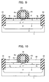
- a sidewall dielectric film 25 formed of a silicon nitride film As shown in Fig. 9, fabricate on a lateral wall of the gate electrode 6 a sidewall dielectric film 25 formed of a silicon nitride film. And as shown in Fig. 10, let silicon surface portions of source/drain regions be exposed; then, form on such exposed surfaces a silicon layer 26 by selective epitaxial growth methods. This is done in order to make the junction planes of p-type layer 2 and n - -type layer 3 stay deeper than a diffusion depth of the next-formed source/drain regions of high impurity concentration.
- n + -type low-resistivity regions 7a of the source/drain are formed.
- the diffusion depth of each low resistivity region 7a is carefully adjusted to ensure that its bottom does not reach the underlying p-type layer 2.
- an interlayer dielectric (ILD) film 27 is deposited; then, form required contact holes therein for embedment of contact plugs 28 made of tungsten (W) or other similar suitable materials.
- the process to be done thereafter includes the step of forming a pattern of metallic on-chip leads on or above the ILD film 27.
- the SODELFET embodying the invention is specifically arranged so that the p-type layer 4 of the channel region is fabricated causing its junction depth to be less or "shallower" than that of the source/drain extension regions 7b while at the same time letting the thickness of n - -type layer 3 be relatively significant to thereby ensure that the bottom surface of a respective one of the source/drain low-resistivity regions 7a resides within the n - -type layer 3.
- higher carrier mobility in the channel region is guaranteed owing to vertical electric field relaxation effects; in addition, it becomes possible to greatly suppress or minimize creation of any possible short-channel effects even in sub-micron regions.
- the gate electrode 6 is comprised of metal electrode 6a.
- the metal electrode 6a may be made of TiN, WN or the like.
- the metal electrode 6a having two work functions are the ones using in combination two different conductive materials ⁇ such as TiN and WN or, alternatively, W and WN.
- any desired threshold voltage is attainable by use of such metal electrode 6a with appropriate work functions in a way pursuant to the threshold voltage required.
- the gate electrode may be formed of polysilicon film pursuant to the threshold voltage required.
- the p-type layer 4 may be replaced with either a SiGe or Si/SiGe distortion alloy layer in order to further improve the carrier mobility of the channel region.
- a SiGe or Si/SiGe distortion alloy layer in order to further improve the carrier mobility of the channel region.
- the use of such layer makes it possible to obtain SODELFETs with much higher current drivabilities. The same goes with any one of the following embodiments as will be discussed below.
- FIG. 14 This diagram depicts a sectional view of an SODELFET structure capable of preventing any punch-through with increased reliability in accordance with a second embodiment of the invention, wherein the depiction here is shown in a way corresponding to Fig. 1.
- This embodiment is similar to that of Fig. 1 except that p-type layers 9 are additionally provided as "halo" regions. These layers are buried in the n - -type layer 3 at locations immediately beneath the source/drain extension regions 7b, respectively.
- appropriate value setting of the impurity concentration and thickness of p-type layer 4 enables accomplishment of the intended FD-SODELFET device.
- letting p-type layer 4 have a further increased impurity concentration makes it possible to obtain a PD-SODELFET.
- p/n - /p multilayer structures may be formed in substantially the same way, i.e. through combined effectuation of epitaxial growth and ion implantation into the entire surface of a substrate.
- similar results are obtainable by use of selective ion implantation techniques ⁇ in this case, the p/n - /p structures are fabricated in units of channel regions of respective transistors involved.
- FIG. 15 there is shown in a manner corresponding to Fig. 1 a sectional view of an SODELFET also embodying the invention, which employs selective ion implantation to selectively fabricate the intended p/n - /p junction multilayer structure in a specified region immediately beneath a gate electrode.
- arsenic (As) ion implantation is selectively done only at a channel body forming portion of an undoped or "nondoped" epitaxially grown silicon layer 10, thereby forming an n - -type layer 3.
- the resulting extension regions 7b of source/drain diffusion layers 7 are such that the bottom surface of each is in contact with its underlying n - -type layer 3 while a respective n + -type low-resistivity region 7a has its bottom face residing within the nondoped silicon layer 10.
- n - -type layer 3 Forming the n - -type layer 3 exclusively at a selected portion just beneath the channel region in this way forces the bottom surfaces of source/drain low-resistivity regions 7a to stay within the nondoped, intrinsic ("i"-type) silicon layer 10. This makes it possible to further reduce the source/drain junction capacitance values.
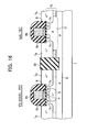
- FIG. 16 A structure of main part of an LSI chip with an FD-SODELFET and a normal bulk FET integrated together is depicted in cross-section in Fig. 16, wherein the FD-SODELFET is the same in principle as that of the third embodiment stated supra.
- the illustrative "hybrid" LSI device structure will now be explained in accordance with a flow of its fabrication process steps.
- an undoped or nondoped silicon layer 10 epitaxially grow on a silicon substrate 1 with a p-type layer formed therein.
- the p-type layer 2 may be selectively formed by ion implantation only in an SODELFET region, rather than is formed to cover an entire surface of the substrate.
- the FD-SODELFET region is subjected, prior to formation of a gate electrode 6, to selective ion implantation similar to that discussed in conjunction with the fourth embodiment, thereby sequentially forming an n-type layer 3 and p-type layer 4.
- the epitaxially grown nondoped silicon layer 10 is subject to another selective ion implantation, forming a p-type bulk layer (i.e., channel body) 31 that is deep sufficient to reach the underlying p-type layer 2. Further, channel ion implantation may be done as occasion demands.
- source/drain's n-type extension regions 7b and n + -type low-resistivity regions 7a substantially simultaneously.
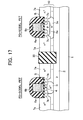
- a hybrid LSI device structure also embodying the invention with an FD-SODELFET and a PD-SODELFET integrated together is shown in Fig. 17, wherein the PD-SODELFET is a partially depletable element which lacks full depletability even upon formation of a channel inversion layer.
- the FD-SODELFET shown is manufacturable by similar process to that shown in Fig. 16.
- the PD-SODELFET its n - -type layer 3a and p-type layer 4a are sequentially fabricated under specific ion implantation conditions different from the FD-SODELFET.
- the n - -type layer 3a of PD-SODELFET may be the same in process conditions as an n - -type layer 3 on the FD-SODELFET side.
- At least the PD-SODELFET's p-type layer 4a is to be formed in such a manner that it is greater both in impurity concentration and in thickness than the p-type layer 4 of FD-SODELFET.
- the p-type layer 4a is greater or "deeper" in diffusion depth than source/drain extension regions 7b and yet shallower than n + -type low-resistivity regions 7a.
- p-type layer 4a and n - -type layer 3a are selectively formed at a location immediately beneath a channel region associated therewith.
- the n - -type layer 3a has its opposite terminate end portions as contacted with source/drain extension regions 7b respectively.
- Fig. 18 demonstrates an exemplary plot of impurity concentration distribution of a p/n - /p junction multilayer structure of the PD-SODELFET in comparison with that of FD-SODELFET shown in Fig. 2.
- the p-type layer 4a's boron concentration is higher than that of Fig. 2 by about one order of magnitude.
- the intended PD-SODELFET is obtained which is higher in threshold voltage than the FD-SODELFET and permits p-type layer 4a to be partially depleted upon formation of a channel inversion layer.
- p-type layer 4a is surrounded by a depletion layer occurring between itself and extension region 7b and the fully depleted n - -type layer 3a, thereby becoming an electrically "floating" p-type layer.
- Fig. 19 is a graph showing drain voltage Vd versus drain current Id characteristics of the above-noted PD-SODELFET with gate voltage Vg as a parameter, which have been obtained through computation.
- the gate length Lg is set at 70 nm
- the drain current Id behaves to rapidly increase in intensity at a certain value of drain voltage Vd.
- This is known as "kink” characteristics among those skilled in the semiconductor device art.
- This kink instability is the property unique to PD-SODELFETs, which is obtainable by virtual threshold voltage drop-down occurring due to partial depletion of the p-type layer 4a. Practically this kink property takes place upon virtual reduction of the threshold voltage, which in turn is caused by a mechanism which follows: upon exceeding of a certain drain voltage, holes as created by impact ionization are stored or accumulated at the p-type layer.
- FIG. 20 This is a graph showing experimental data of the PD-SODELFET for demonstrating a typical plot of voltage vb of the channel body (i.e. p-type layer 4a) as a function of time with epitaxially grown silicon layer 10's thickness as a parameter when causing a drain voltage Vd to rapidly vary in potential with time in a pulse-like fashion as indicated by dotted lines, while letting a gate voltage Vg kept constant.
- the drain voltage Vd changes, the body potential Vb changes accordingly, which in turn well demonstrates that p-type layer 4a is substantially in the floating state.
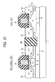
- Fig. 21 shows an integrated structure having an PD-SODELFET and a normal bulk FET in accordance with sixth embodiment.
- the respective channel body structures of the PD-SODELFET and the bulk FET are similar to that of the embodiment of Fig. 16.
- the p-type layer 4 of the PD-SEDELFET is, however, formed to have a higher impurity concentration than that of the FD-SODELFET in Fig. 16. Whereby, the p-type layer 4 becomes to be partially depleted when a channel inversion layer is formed.
- gate threshold voltage thereof becomes too high.
- the threshold voltage of the bulk FET may be set to lower. AS a result, it is possible to obtain a high current drivable bulk FET.
- FD-SODELFETs and PD-SODELFETs in Figs. 16, 17 and 21 are modifiable so that each is structured so that p-type layers 9 are buried as halo regions at locations right below the source/drain extension regions 7b respectively, as in the embodiment of Fig. 14.
- Fig. 22 depicts a configuration of NAND gate circuitry, which is arranged using a serial connection of three n-channel transistors QN1 to QN3 and a parallel combination of p-channel transistors QP1-QP3.
- the n-channel transistors QN1 to QN3 serially connected between an output terminal OUT and ground terminal Vss with the gates serving as input terminals A, B and C, respectively.
- the p-channel transistors QP1 to QP3 are connected in parallel between the output terminal OUTPUT and a power supply terminal Vdd with the gates being connected to the respective input terminals A to C.
- the transistors QN1-QN3 are formed of FD-SODELFETs, PD-SODELFETs shown in Fig. 1, or PD-SODELFETs shown in Fig. 17 which are inherently less in substrate bias influence than bulk FETs.
- the p-channel transistors QP1-QP3 are designed to employ bulk FETs that have the same structure shown in Fig. 16 and are less in current leakage otherwise occurring due to the presence of possible parasitic bipolar transistor components. With such an arrangement, it is possible to attain higher operation stability and also higher noise margins.
- n-channel transistors QN11-QN13 that are connected between nodes N1 and N2 in parallel, are switching devices with the gates serving as input terminals A, B, and C, respectively.
- a precharging p-channel transistor QP11 of which gate is driven by precharge signal PRE.
- n-channel activation transistor QN14 is disposed between the node N2 and a ground terminal Vss, of which gate is driven by clock signal CK.
- the node N1 is coupled to an output terminal OUT through an inverter INV.
- a p-channel transistor QP12 as controlled by a voltage appearing at output terminal OUT.
- node N1 With such clock-driven dynamic circuit, it becomes difficult to achieve high speed operations if the node N1 is significant in capacitance.
- analog circuits and/or sense amplifier circuits for use with semiconductor memory devices are typically formed of differential amplifiers.
- a differential amplifier made up from two complementary metal oxide semiconductor (CMOS) circuits is under a strict requirement that such two CMOS circuits are exactly identical in threshold voltage to each other.
- CMOS complementary metal oxide semiconductor
- SODELFETs embodying the invention these can experience deviation or "offset" in threshold voltage values under influence of the history in the past in view of the fact that a channel body region(s) is/are in the floating state. This makes it rather difficult to align the threshold voltage levels of two CMOS circuits in any events. Consequently, even in the LSI chip using SODELFETs embodying the invention, it will be preferable to employ "different-FET-for-different-part" schemes for using bulk FETs for the differential amplifiers.
- LSIs using the FD-SODELFETs embodying the invention it is also effective to additionally comprise substrate bias application circuitry for selectively applying a substrate bias voltage for threshold voltage adjustment to the p-type layer at lower part in case p/n - /p junction multilayer structures are provided separately in units of on-chip elements.
- substrate bias application circuitry for selectively applying a substrate bias voltage for threshold voltage adjustment to the p-type layer at lower part in case p/n - /p junction multilayer structures are provided separately in units of on-chip elements.
- Fig. 24 which shows a plot of drain current Id of the Fig.
- Each of the NAND gate circuit shown in Fig. 22 and the dynamic domino circuit shown in Fig. 23 may be configured to employ a combination of SOIFETs and bulk FETs which are formed in a partial SOI substrate.
- Fig.25 shows an integrated structure of an SOIFET and a bulk FET integrally formed in a partial SOI substrate.
- the partial SOI substrate has an SOI region where a thin silicon layer 103 is formed over a silicon substrate 101 with an insulating film 102 buried therebetween, and a bulk region where no insulating film is buried.
- the SOIFET is formed in the silicon layer 103 of the SOI region.
- the SOIFET has a gate electrode 202 formed above the silicon layer 103 with a gate insulating film 201 interposed therebetween, and source/drain diffused layers 203.
- the source/drain diffused layers 203 are formed as to be contacted with the insulating film 102.
- the SOIFET becomes a fully depleted FET.
- an n-type (or p-type) well layer 301 is formed in the bulk region.
- the bulk FET is formed in the bulk region to have a gate electrode 303 formed above the well layer 301 with a gate insulating film 302 interposed therebetween, and source/drain diffused layers 304.
- n-channel transistors QN1-QN3 in the NAND gate circuit shown in Fig. 22 are formed of SOIFETs as shown in Fig. 25.
- p-channel transistors QP1-QP3 in the NAND gate circuit are formed of bulk FET shown in Fig. 25.
- n-channel transistors QN11-QN13 in the dynamic domino circuit shown in Fig. 23 are formed of SOIFETs shown in Fig. 25.
- p-channel transistors QP1, QP12 and n-channel transistor QN14 in the dynamic domino circuit are formed of bulk FET shown in Fig. 25.
Landscapes
- Insulated Gate Type Field-Effect Transistor (AREA)
- Metal-Oxide And Bipolar Metal-Oxide Semiconductor Integrated Circuits (AREA)
Claims (16)
- Halbleitervorrichtung, welche ein Halbleitersubstrat (1) und einen im Halbleitersubstrat (1) ausgebildeten ersten und zweiten Transistor hat, wobei jeder Transistor eine Gate-Elektrode (6), welche über dem Halbleitersubstrat (1) mit einem dazwischen eingelegten Gate-Dielektrikumfilm (5) ausgebildet ist, und Source- und Drain-Diffusionsschichten (7), welche im Halbleitersubstrat gegenüberliegend mit einem dazwischen eingeschobenen Kanal-Bereich an einer Stelle unmittelbar neben der Gate-Elektrode ausgebildet sind, enthält, wobei:der erste Transistor ferner eine erste mit Störstellen dotierte Schicht (4) von einem ersten Leitfähigkeitstyp, welche in einem Oberflächen-Kanal-Bereich zwischen den Source-/Drain-Diffusionsschichten (7) ausgebildet ist, eine zweite mit Störstellen dotierte Schicht (3) von einem zweiten Leitfähigkeitstyp, welche unterhalb der ersten mit Störstellen dotierten Schicht (4) ausgebildet ist, und eine dritte mit Störstellen dotierte Schicht (2) vom ersten Leitfähigkeitstyp, welche unterhalb der zweiten mit Störstellen dotierten Schicht (3) ausgebildet ist, enthält;die Source-/Drain-Diffusionsschichten (7) des ersten Transistors jeweils aus einem Niedrigwiderstands-Bereich (7a) und einem Erstreckungs-Bereich (7b), welcher derart ausgebildet ist, dass er sich von diesem Niedrigwiderstands-Bereich (7a) aus zur Kanal-Bereichsseite erstreckt, ausgebildet sind, wobei der Erstreckungs-Bereich (7b) eine niedrigere Störstellen-Konzentration und eine geringere Tiefe als der Niedrigwiderstands-Bereich (7a) hat;die erste mit Störstellen dotierte Schicht (4) eine Störstellen-Konzentration und Dicke hat, welche derart bestimmt sind, um zu bewirken, dass diese Schicht (4) beim Ausbilden einer Kanal-Inversionsschicht vollständig oder teilweise erschöpft ist; unddie zweite mit Störstellen dotierte Schicht (3) derart ausgebildet ist, dass die Tiefe von ihrer Kontaktstelle mit der dritten mit Störstellen dotierten Schicht (2) größer als die Kontaktstellen-Tiefe der Source-/Drain-Diffusionsschichten (7) ist, während ihre Störstellen-Konzentration und Dicke derart bestimmt sind, um sicherzustellen, dass diese Schicht (3) aufgrund eines eingebauten Potentials, welches zwischen der ersten und dritten mit Störstellen dotierten Schicht (4, 2) erzeugbar ist, vollständig erschöpft ist, und dadurch gekennzeichnet, dassdie erste mit Störstellen dotierte Schicht (4) in ihrer Kontaktstellen-Tiefe gleich oder geringer ist als der Erstreckungs-Bereich (7b).
- Vorrichtung nach Anspruch 1, dadurch gekennzeichnet, dass die erste mit Störstellen dotierte Schicht in ihrer Störstellen-Konzentration und Dicke derart bestimmt ist, dass sie beim Ausbilden von einer Kanal-Inversionsschicht vollständig erschöpft ist.
- Vorrichtung nach Anspruch 1, dadurch gekennzeichnet, dass die erste mit Störstellen dotierte Schicht in ihrer Störstellen-Konzentration und Dicke derart bestimmt ist, dass sie beim Ausbilden von einer Kanal-Inversionsschicht teilweise erschöpft ist.
- Vorrichtung nach Anspruch 1, dadurch gekennzeichnet, dass sich die Boden-Oberfläche des Niedrigwiderstands-Bereichs (7a) des ersten Transistors innerhalb der zweiten mit Störstellen dotierten Schicht (3) befindet.
- Vorrichtung nach Anspruch 1, dadurch gekennzeichnet, dass die erste und zweite mit Störstellen dotierte Schicht (4, 3) Epitaxie-Schichten sind, welche mit Ionen implantierte Störstellen enthalten, und auf der dritten mit Störstellen dotierten Schicht (2) bereitgestellt sind.
- Vorrichtung nach Anspruch 5, dadurch gekennzeichnet, dass sich die zweite mit Störstellen dotierte Schicht (3) zwischen den Source-/Drain-Diffusionsschichten (7) des ersten Transistors befindet, und dass die Niedrigwiderstands-Bereiche (7a) des ersten Transistors Boden-Oberflächen haben, welche sich innerhalb der zweiten mit Störstellen dotierten Schicht (3) befinden.
- Vorrichtung nach Anspruch 1, dadurch gekennzeichnet, dass sie ferner eine vierte mit Störstellen dotierte Schicht (9) enthält, welche eingegraben ist, um mit den Erstreckungs-Bereichen (7b) des ersten Transistors in Kontakt zu kommen.
- Vorrichtung nach Anspruch 1, dadurch gekennzeichnet, dass die Niedrigwiderstands-Bereiche (7a) der Source-/Drain-Erstreckungsbereiche (7) des ersten Transistors derart ausgebildet sind, dass sie Kopf-Oberflächen haben, deren Pegel höher ist als der des Gate-Dielektrikumfilms (5).
- Vorrichtung nach Anspruch 1, dadurch gekennzeichnet, dass die Gate-Elektroden (6) des ersten und zweiten Transistors jeweils einen Metallfilm (6a) haben, welcher mit ihrem unterliegenden Gate-Dielektrikumfilm (5) in Kontakt ist.
- Vorrichtung nach Anspruch 1, dadurch gekennzeichnet, dass die Gate-Elektroden (6) des ersten und zweiten Transistors aus einem Metallfilm ausgebildet sind.
- Vorrichtung nach Anspruch 3, dadurch gekennzeichnet, dass die Gate-Elektroden (6) des ersten und zweiten Transistors aus einem Polysiliziumfilm ausgebildet sind.
- Vorrichtung nach Anspruch 1, dadurch gekennzeichnet, dass der zweite Transistor in einem Abschnitt des Halbleitersubstrats (1), welcher unmittelbar neben der Gate-Elektrode (6) liegt, eine Hauptschicht (31) des ersten Leitfähigkeitstyps hat, welche als eine mit Störstellen dotierte Schicht tiefer als die Source-/Drain-Diffusionsschichten (7) ausgebildet ist.
- Vorrichtung nach Anspruch 1, dadurch gekennzeichnet, dass der zweite Transistor ferner eine fünfte mit Störstellen dotierte Schicht (4a) des ersten Leitfähigkeitstyps, wobei sie im Kanal-Bereich zwischen den Source-/Drain-Diffusionsschichten (7) ausgebildet ist, eine sechste mit Störstellen dotierte Schicht (3a) des zweiten Leitfähigkeitstyps, wobei sie unterhalb der fünften mit Störstellen dotierten Schicht (4a) ausgebildet ist, und eine siebte mit Störstellen dotierte Schicht (2) der ersten Leitfähigkeit, wobei sie unterhalb der sechsten mit Störstellen dotierte Schicht (3a) ausgebildet ist, enthält, wobei bei der fünften mit Störstellen dotierten Schicht (4a) ihre Kontaktstellen-Tiefe größer als die der ersten mit Störstellen dotierten Schicht (4) des ersten Transistors ist, und sie ebenfalls eine Störstellen-Konzentration und Dicke hat, welche derart bestimmt sind, um sicherzustellen, dass diese Schicht (4a) beim Ausbilden von einer Kanal-Inversionsschicht teilweise erschöpft ist, wobei bei der sechsten mit Störstellen dotierten Schicht (3a) ihre Tiefe von ihrer Kontaktstelle mit der siebten mit Störstellen dotierten Schicht (2) größer als die Kontaktstellen-Tiefe der Source-/Drain-Diffusionsschichten (7) ist, während die sechste Schicht (3a) durch ein eingebautes Potential, welches zwischen der fünften und siebten mit Störstellen dotierten Schicht (4a, 2) erzeugbar ist, vollständig erschöpft belassen wird.
- Vorrichtung nach Anspruch 13, dadurch gekennzeichnet, dass die fünfte mit Störstellen dotierte Schicht (4a) selektiv derart ausgebildet ist, dass ihre Kontaktstellen-Tiefe größer als die der Erstreckungs-Bereiche (7b) der Source-/Drain-Diffusionsschichten (7) ist, wohingegen die sechste mit Störstellen dotierte Schicht (3a) selektiv derart ausgebildet ist, dass ihre gegenüberliegenden Endabschnitte in Kontakt mit den Erstreckungs-Bereichen (7b) der Source-/Drain-Diffusionsschichten (7) belassen werden.
- Vorrichtung nach Anspruch 13, dadurch gekennzeichnet, dass die fünfte und sechste mit Störstellen dotierte Schicht (4a, 3a) mit Ionen implantierte Bereiche der Halbleiter Epitaxie-Schicht (10) sind, welche darin die dritte und siebte mit Störstellen dotierte Schicht (2) ausgebildet hat.
- Vorrichtung nach Anspruch 13, dadurch gekennzeichnet, dass die Niedrigwiderstands-Bereiche (7a) der Source-/Drain-Erstreckungsbereiche (7) des zweiten Transistors derart ausgebildet sind, dass deren Kopf-Oberflächen eine höheren Pegel haben als der Gate-Dielektrikumfilm (5).
Applications Claiming Priority (2)
| Application Number | Priority Date | Filing Date | Title |
|---|---|---|---|
| JP2001010449 | 2001-01-18 | ||
| JP2001010449 | 2001-01-18 |
Publications (3)
| Publication Number | Publication Date |
|---|---|
| EP1225622A2 EP1225622A2 (de) | 2002-07-24 |
| EP1225622A3 EP1225622A3 (de) | 2003-11-12 |
| EP1225622B1 true EP1225622B1 (de) | 2006-08-16 |
Family
ID=18877760
Family Applications (1)
| Application Number | Title | Priority Date | Filing Date |
|---|---|---|---|
| EP02000298A Expired - Lifetime EP1225622B1 (de) | 2001-01-18 | 2002-01-16 | Halbleiteranordnung |
Country Status (6)
| Country | Link |
|---|---|
| US (2) | US6930361B2 (de) |
| EP (1) | EP1225622B1 (de) |
| KR (1) | KR20020062200A (de) |
| CN (1) | CN1220271C (de) |
| DE (1) | DE60213889T2 (de) |
| TW (1) | TWI288472B (de) |
Families Citing this family (35)
| Publication number | Priority date | Publication date | Assignee | Title |
|---|---|---|---|---|
| US7217977B2 (en) * | 2004-04-19 | 2007-05-15 | Hrl Laboratories, Llc | Covert transformation of transistor properties as a circuit protection method |
| US6804502B2 (en) | 2001-10-10 | 2004-10-12 | Peregrine Semiconductor Corporation | Switch circuit and method of switching radio frequency signals |
| US7432136B2 (en) * | 2002-05-06 | 2008-10-07 | Advanced Micro Devices, Inc. | Transistors with controllable threshold voltages, and various methods of making and operating same |
| US7129142B2 (en) | 2002-06-11 | 2006-10-31 | Advanced Micro Devices, Inc. | Method of forming doped regions in the bulk substrate of an SOI substrate to control the operational characteristics of transistors formed thereabove, and an integrated circuit device comprising same |
| US7049667B2 (en) | 2002-09-27 | 2006-05-23 | Hrl Laboratories, Llc | Conductive channel pseudo block process and circuit to inhibit reverse engineering |
| JP4846239B2 (ja) * | 2002-12-13 | 2011-12-28 | エイチアールエル ラボラトリーズ,エルエルシー | ウェル注入を用いた集積回路の改変 |
| JP4590884B2 (ja) * | 2003-06-13 | 2010-12-01 | 株式会社デンソー | 半導体装置およびその製造方法 |
| US7202133B2 (en) | 2004-01-21 | 2007-04-10 | Chartered Semiconductor Manufacturing, Ltd. | Structure and method to form source and drain regions over doped depletion regions |
| US7242063B1 (en) | 2004-06-29 | 2007-07-10 | Hrl Laboratories, Llc | Symmetric non-intrusive and covert technique to render a transistor permanently non-operable |
| US7019356B2 (en) * | 2004-08-02 | 2006-03-28 | Texas Instruments Incorporated | Memory device with reduced cell area |
| JP4664631B2 (ja) * | 2004-08-05 | 2011-04-06 | 株式会社東芝 | 半導体装置及びその製造方法 |
| US7326977B2 (en) * | 2004-10-04 | 2008-02-05 | Northrop Grumman Corporation | Low noise field effect transistor |
| JP2006140396A (ja) * | 2004-11-15 | 2006-06-01 | Toshiba Corp | 半導体集積回路装置およびその製造方法 |
| KR100613294B1 (ko) * | 2004-12-30 | 2006-08-21 | 동부일렉트로닉스 주식회사 | 단채널 효과가 개선되는 모스 전계효과 트랜지스터 및 그제조 방법 |
| JP2006310625A (ja) * | 2005-04-28 | 2006-11-09 | Toshiba Corp | 半導体記憶装置 |
| US9653601B2 (en) | 2005-07-11 | 2017-05-16 | Peregrine Semiconductor Corporation | Method and apparatus for use in improving linearity of MOSFETs using an accumulated charge sink-harmonic wrinkle reduction |
| US20080076371A1 (en) | 2005-07-11 | 2008-03-27 | Alexander Dribinsky | Circuit and method for controlling charge injection in radio frequency switches |
| USRE48965E1 (en) | 2005-07-11 | 2022-03-08 | Psemi Corporation | Method and apparatus improving gate oxide reliability by controlling accumulated charge |
| US7910993B2 (en) | 2005-07-11 | 2011-03-22 | Peregrine Semiconductor Corporation | Method and apparatus for use in improving linearity of MOSFET's using an accumulated charge sink |
| US7890891B2 (en) * | 2005-07-11 | 2011-02-15 | Peregrine Semiconductor Corporation | Method and apparatus improving gate oxide reliability by controlling accumulated charge |
| US7776725B2 (en) * | 2005-09-12 | 2010-08-17 | International Business Machines Corporation | Anti-halo compensation |
| US20080001183A1 (en) * | 2005-10-28 | 2008-01-03 | Ashok Kumar Kapoor | Silicon-on-insulator (SOI) junction field effect transistor and method of manufacture |
| US20070145495A1 (en) * | 2005-12-27 | 2007-06-28 | Intel Corporation | Method of fabricating a MOSFET transistor having an anti-halo for modifying narrow width device performance |
| US8168487B2 (en) | 2006-09-28 | 2012-05-01 | Hrl Laboratories, Llc | Programmable connection and isolation of active regions in an integrated circuit using ambiguous features to confuse a reverse engineer |
| US8652912B2 (en) | 2006-12-08 | 2014-02-18 | Micron Technology, Inc. | Methods of fabricating a transistor gate including cobalt silicide |
| US20090045458A1 (en) * | 2007-08-15 | 2009-02-19 | Advanced Micro Devices, Inc. | Mos transistors for thin soi integration and methods for fabricating the same |
| US20090166625A1 (en) | 2007-12-28 | 2009-07-02 | United Microelectronics Corp. | Mos device structure |
| JP5211689B2 (ja) * | 2007-12-28 | 2013-06-12 | 富士通セミコンダクター株式会社 | 半導体装置及びその製造方法 |
| US8232599B2 (en) * | 2010-01-07 | 2012-07-31 | International Business Machines Corporation | Bulk substrate FET integrated on CMOS SOI |
| WO2011115893A2 (en) | 2010-03-15 | 2011-09-22 | Micron Technology, Inc. | Techniques for providing a semiconductor memory device |
| JP5586546B2 (ja) * | 2011-03-23 | 2014-09-10 | 株式会社東芝 | 半導体装置 |
| CN103000671B (zh) * | 2011-09-16 | 2015-07-15 | 中国科学院微电子研究所 | Mosfet及其制造方法 |
| US20170338302A1 (en) * | 2016-05-23 | 2017-11-23 | Infineon Technologies Ag | Power Semiconductor Device with Charge Balance Design |
| US9837507B1 (en) * | 2016-09-30 | 2017-12-05 | Taiwan Semiconductor Manufacturing Co., Ltd. | Semiconductor device and manufacturing method thereof |
| CN119451166B (zh) * | 2024-10-25 | 2025-10-14 | 长鑫科技集团股份有限公司 | 半导体结构及其制作方法以及半导体器件 |
Family Cites Families (16)
| Publication number | Priority date | Publication date | Assignee | Title |
|---|---|---|---|---|
| JPS6050960A (ja) | 1983-08-30 | 1985-03-22 | Toshiba Corp | 半導体装置 |
| JPS62128175A (ja) | 1985-11-29 | 1987-06-10 | Hitachi Ltd | 半導体装置 |
| JPH065745B2 (ja) | 1986-07-31 | 1994-01-19 | 株式会社日立製作所 | 半導体装置 |
| JP3119370B2 (ja) | 1991-03-18 | 2000-12-18 | キヤノン株式会社 | 絶縁ゲートトランジスタ及び半導体集積回路 |
| JP2899122B2 (ja) | 1991-03-18 | 1999-06-02 | キヤノン株式会社 | 絶縁ゲートトランジスタ及び半導体集積回路 |
| JPH0645598A (ja) | 1992-07-21 | 1994-02-18 | Fujitsu Ltd | 半導体装置及びその製造方法 |
| JPH07131002A (ja) | 1993-11-04 | 1995-05-19 | Victor Co Of Japan Ltd | 半導体装置及びその製造方法 |
| US5463237A (en) | 1993-11-04 | 1995-10-31 | Victor Company Of Japan, Ltd. | MOSFET device having depletion layer |
| JP2858622B2 (ja) | 1993-11-24 | 1999-02-17 | 日本ビクター株式会社 | 半導体装置 |
| JPH07312423A (ja) * | 1994-05-17 | 1995-11-28 | Hitachi Ltd | Mis型半導体装置 |
| JPH07335837A (ja) | 1994-06-03 | 1995-12-22 | Hitachi Ltd | 半導体装置および論理回路 |
| US5698884A (en) | 1996-02-07 | 1997-12-16 | Thunderbird Technologies, Inc. | Short channel fermi-threshold field effect transistors including drain field termination region and methods of fabricating same |
| JP3423161B2 (ja) | 1996-10-11 | 2003-07-07 | 三洋電機株式会社 | 半導体装置の製造方法 |
| US6163053A (en) * | 1996-11-06 | 2000-12-19 | Ricoh Company, Ltd. | Semiconductor device having opposite-polarity region under channel |
| JP3383219B2 (ja) | 1998-05-22 | 2003-03-04 | シャープ株式会社 | Soi半導体装置及びその製造方法 |
| US6162694A (en) * | 1998-11-25 | 2000-12-19 | Advanced Micro Devices, Inc. | Method of forming a metal gate electrode using replaced polysilicon structure |
-
2001
- 2001-12-14 TW TW090131024A patent/TWI288472B/zh not_active IP Right Cessation
-
2002
- 2002-01-11 US US10/042,264 patent/US6930361B2/en not_active Expired - Lifetime
- 2002-01-16 EP EP02000298A patent/EP1225622B1/de not_active Expired - Lifetime
- 2002-01-16 DE DE60213889T patent/DE60213889T2/de not_active Expired - Lifetime
- 2002-01-17 CN CNB021020434A patent/CN1220271C/zh not_active Expired - Fee Related
- 2002-01-17 KR KR1020020002752A patent/KR20020062200A/ko not_active Ceased
-
2005
- 2005-06-03 US US11/143,715 patent/US7400016B2/en not_active Expired - Fee Related
Also Published As
| Publication number | Publication date |
|---|---|
| EP1225622A2 (de) | 2002-07-24 |
| US7400016B2 (en) | 2008-07-15 |
| US20020093064A1 (en) | 2002-07-18 |
| DE60213889D1 (de) | 2006-09-28 |
| CN1366347A (zh) | 2002-08-28 |
| US20050218449A1 (en) | 2005-10-06 |
| TWI288472B (en) | 2007-10-11 |
| CN1220271C (zh) | 2005-09-21 |
| US6930361B2 (en) | 2005-08-16 |
| EP1225622A3 (de) | 2003-11-12 |
| DE60213889T2 (de) | 2007-09-06 |
| KR20020062200A (ko) | 2002-07-25 |
Similar Documents
| Publication | Publication Date | Title |
|---|---|---|
| EP1225622B1 (de) | Halbleiteranordnung | |
| US6380590B1 (en) | SOI chip having multiple threshold voltage MOSFETs by using multiple channel materials and method of fabricating same | |
| US6287908B1 (en) | Transistor device configurations for high voltage applications and improved device performance | |
| US7259428B2 (en) | Semiconductor device using SOI structure having a triple-well region | |
| KR100562539B1 (ko) | 벌크 씨모스 구조와 양립 가능한 에스오아이 구조 | |
| US4951102A (en) | Trench gate VCMOS | |
| US6100143A (en) | Method of making a depleted poly-silicon edged MOSFET structure | |
| CN107425057B (zh) | 包括在衬底中设有栅极电极区的晶体管的半导体结构及其形成方法 | |
| EP0814502A1 (de) | Komplementäre Halbleiteranordnung und Verfahren zur Herstellung | |
| KR20040102052A (ko) | 다중-두께 매립 산화물층 위에 형성된 반도체 디바이스 및그 제조 방법 | |
| KR100276775B1 (ko) | Mos 트랜지스터 및 그 제조 방법 | |
| KR100723076B1 (ko) | 반도체 디바이스 | |
| JPH06224428A (ja) | 電界効果トランジスタ及びその形成方法 | |
| KR100232813B1 (ko) | 저 누설 soi 집적 회로를 제조하기 위한 방법 | |
| US6933572B2 (en) | Field-shielded SOI-MOS structure free from floating body effect, and method of fabrication therefor | |
| US6627505B2 (en) | Method of producing SOI MOSFET having threshold voltage of central and edge regions in opposite directions | |
| JP2001156290A (ja) | 半導体装置 | |
| JPH11224946A (ja) | 半導体装置およびその作製方法 | |
| US6476430B1 (en) | Integrated circuit | |
| JPH11135799A (ja) | 半導体集積回路及びその製造方法 | |
| US5602410A (en) | Off-state gate-oxide field reduction in CMOS | |
| JP2951292B2 (ja) | 相補型半導体装置及びその製造方法 | |
| US6388288B1 (en) | Integrating dual supply voltages using a single extra mask level | |
| US6882013B2 (en) | Transistor with reduced short channel effects and method | |
| US20040053456A1 (en) | Mosfet with short channel structure and formation method thereof |
Legal Events
| Date | Code | Title | Description |
|---|---|---|---|
| PUAI | Public reference made under article 153(3) epc to a published international application that has entered the european phase |
Free format text: ORIGINAL CODE: 0009012 |
|
| 17P | Request for examination filed |
Effective date: 20020116 |
|
| AK | Designated contracting states |
Kind code of ref document: A2 Designated state(s): AT BE CH CY DE DK ES FI FR GB GR IE IT LI LU MC NL PT SE TR |
|
| AX | Request for extension of the european patent |
Free format text: AL;LT;LV;MK;RO;SI |
|
| RIC1 | Information provided on ipc code assigned before grant |
Ipc: 7H 01L 27/088 B Ipc: 7H 01L 29/10 B Ipc: 7H 01L 21/78 B Ipc: 7H 01L 21/336 A Ipc: 7H 01L 29/78 B Ipc: 7H 01L 27/12 B |
|
| PUAL | Search report despatched |
Free format text: ORIGINAL CODE: 0009013 |
|
| AK | Designated contracting states |
Kind code of ref document: A3 Designated state(s): AT BE CH CY DE DK ES FI FR GB GR IE IT LI LU MC NL PT SE TR |
|
| AX | Request for extension of the european patent |
Extension state: AL LT LV MK RO SI |
|
| 17Q | First examination report despatched |
Effective date: 20040202 |
|
| AKX | Designation fees paid |
Designated state(s): DE GB |
|
| RTI1 | Title (correction) |
Free format text: SEMICONDUCTOR DEVICE |
|
| GRAP | Despatch of communication of intention to grant a patent |
Free format text: ORIGINAL CODE: EPIDOSNIGR1 |
|
| GRAS | Grant fee paid |
Free format text: ORIGINAL CODE: EPIDOSNIGR3 |
|
| GRAA | (expected) grant |
Free format text: ORIGINAL CODE: 0009210 |
|
| AK | Designated contracting states |
Kind code of ref document: B1 Designated state(s): DE GB |
|
| REG | Reference to a national code |
Ref country code: GB Ref legal event code: FG4D |
|
| REF | Corresponds to: |
Ref document number: 60213889 Country of ref document: DE Date of ref document: 20060928 Kind code of ref document: P |
|
| PLBE | No opposition filed within time limit |
Free format text: ORIGINAL CODE: 0009261 |
|
| STAA | Information on the status of an ep patent application or granted ep patent |
Free format text: STATUS: NO OPPOSITION FILED WITHIN TIME LIMIT |
|
| 26N | No opposition filed |
Effective date: 20070518 |
|
| GBPC | Gb: european patent ceased through non-payment of renewal fee |
Effective date: 20070116 |
|
| PG25 | Lapsed in a contracting state [announced via postgrant information from national office to epo] |
Ref country code: GB Free format text: LAPSE BECAUSE OF NON-PAYMENT OF DUE FEES Effective date: 20070116 |
|
| PGFP | Annual fee paid to national office [announced via postgrant information from national office to epo] |
Ref country code: DE Payment date: 20150113 Year of fee payment: 14 |
|
| REG | Reference to a national code |
Ref country code: DE Ref legal event code: R119 Ref document number: 60213889 Country of ref document: DE |
|
| PG25 | Lapsed in a contracting state [announced via postgrant information from national office to epo] |
Ref country code: DE Free format text: LAPSE BECAUSE OF NON-PAYMENT OF DUE FEES Effective date: 20160802 |