EP1214662B1 - System and method for initiating a serial data transfer between two clock domains - Google Patents
System and method for initiating a serial data transfer between two clock domains Download PDFInfo
- Publication number
- EP1214662B1 EP1214662B1 EP00919559A EP00919559A EP1214662B1 EP 1214662 B1 EP1214662 B1 EP 1214662B1 EP 00919559 A EP00919559 A EP 00919559A EP 00919559 A EP00919559 A EP 00919559A EP 1214662 B1 EP1214662 B1 EP 1214662B1
- Authority
- EP
- European Patent Office
- Prior art keywords
- clock
- ratio
- bits
- clock rate
- processor
- Prior art date
- Legal status (The legal status is an assumption and is not a legal conclusion. Google has not performed a legal analysis and makes no representation as to the accuracy of the status listed.)
- Expired - Lifetime
Links
Images




Classifications
-
- G—PHYSICS
- G06—COMPUTING OR CALCULATING; COUNTING
- G06F—ELECTRIC DIGITAL DATA PROCESSING
- G06F13/00—Interconnection of, or transfer of information or other signals between, memories, input/output devices or central processing units
- G06F13/38—Information transfer, e.g. on bus
-
- G—PHYSICS
- G06—COMPUTING OR CALCULATING; COUNTING
- G06F—ELECTRIC DIGITAL DATA PROCESSING
- G06F13/00—Interconnection of, or transfer of information or other signals between, memories, input/output devices or central processing units
- G06F13/38—Information transfer, e.g. on bus
- G06F13/40—Bus structure
- G06F13/4004—Coupling between buses
- G06F13/4027—Coupling between buses using bus bridges
- G06F13/405—Coupling between buses using bus bridges where the bridge performs a synchronising function
- G06F13/4059—Coupling between buses using bus bridges where the bridge performs a synchronising function where the synchronisation uses buffers, e.g. for speed matching between buses
Definitions
- This invention relates to data communications, and more particularly to a system and method for initiating a serial data transfer between a first device clocked according to a first clock and a second device clocked according to a second clock.
- US-A-5 909 563 discloses a computer system for communicating a serial data stream having the features of the preamble of accompanying claim 4, and a method for communicating a serial data stream having the features of the preamble of accompanying claim 1.
- One solution to speeding up transfer rates is to use an asynchronous transfer method so that high transfer rates may be achieved between devices operating at different clock rates.
- the clock is not transmitted with the data.
- One problem that arises is that the asynchronous transfers must be initiated between the devices. What is needed is a system and method for transmitting a data stream between devices operating in differing clock domains, which may have differing clock rates.
- processors are each coupled to a bridge through separate high speed connections, which in one embodiment each include a pair of unidirectional address buses with respective source-synchronous clock lines and a bi-directional data bus with attendant source-synchronous clock lines.
- System memory and graphics may also be coupled to the bridge, as well as an input/output bus.
- a method for initiating a serial data stream between a transmitter and a receiver.
- the transmitter operates according to at least a first clock having a first clock rate
- the receiver operates according to at least a second clock having a second clock rate.
- a ratio between the second clock rate and the first clock rate is an integer number greater than or equal to one.
- the method comprises providing a first state over a serial line between the transmitter and the receiver.
- the method also includes providing one or more start bits over the serial line.
- the start bits indicate a second state different from the first state.
- the method also provides one or more ratio bits over the serial line after the start bit.
- the ratio bits indicate the ratio between the second clock rate and the first clock rate.
- the method receives the one or more start bits. Using a transition between the first state and the second state evident in receiving each of the start bits, the method receives the one or more ratio bits.
- the method also includes receiving a remainder of the serial data stream at appropriate intervals of the second clock rate.
- a computer system comprises a memory, logic, and at least one processor.
- the memory is configured to store initialization information for the computer system.
- the initialization information begins with a start bit and a ratio bit.
- the ratio bit is encoded with the ratio between a second clock rate and a first clock rate.
- the logic is coupled to the memory for transmitting the initialization information.
- the logic is configured to operate according to the first clock rate and to transmit the initialization information at the first clock rate.
- the processor is coupled to receive a first system clock operating at the first clock rate and a second system clock operating at the second clock rate.
- the processor is configured to operate according to the second system clock.
- the processor is further coupled to the logic with a serial line over which to receive the initialization information.
- the logic is configured to transmit the initialization information over the serial line to the processor.
- the logic is further configured to transmit a first state over the serial line prior to the start bit
- the start bit includes a second state different from the first state.
- the processor is further configured to receive the start bit and to use a transition between the first state and the second state evident in receiving the start bit to receive the ratio bit.
- the processor is further configured to decode the ratio bit to determine the first clock rate in order to receive the remainder of the initialization information from the logic.
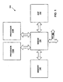
- FIG. 1 a block diagram of an embodiment of a generalized computer system 100 is illustrated.
- a first processor 110A and a second processor 110B each couple to a bridge 130 through separate processor buses. Both the first processor 110A and the second processor 110B are preferably configured to perform memory and I/O operations using their respective processor buses.
- processors 110A and 110B implement the x86 instruction set architecture. Other embodiments may implement any suitable instruction set architecture.
- the bridge 130 is further coupled to a memory 140.
- the memory 140 is preferably configured to store data and instructions accessible to both the first processor 110A and the second processor 110B, as well as other system devices.
- the memory 140 may be comprised of SDRAM (Synchronous Dynamic Random Access Memory), RDRAM (Rambus DRAM) [RDRAM and RAMBUS are registered trademarks of Rambus, Inc.], or any other suitable memory type.
- SDRAM Serial Dynamic Random Access Memory
- RDRAM Random Access Memory
- RAMBUS Random Access Memory
- An advanced graphics port device (AGP) 150 is also optionally coupled to the bridge 130.
- AGP advanced graphics port device
- PCI Peripheral Component Interconnect
- I/O components may be coupled to the PCI bus 160.
- the bridge 130 is often referred to an a northbridge 130, with the bridge (not shown) between the PCI bus 160 and the legacy bus referred to as a southbridge. It is also noted that in the illustrated embodiment, the bridge 130 is the system master for the computer system 100. While the illustrated embodiment includes two processors 110A and 110B, it is noted any number of processors 110 may be included in the computer system 100 as desired.
- ISA Industry Standard Architecture
- the bridge 130 operates to coordinate communications between processors 110A and 110B, the memory 140, and the AGP device 150, as well as devices coupled to the PCI bus, etc.
- the bridge 130 maintains coherency for data transfers among the devices of the computer system 100 by probing processor 110A and/or processor 110B for memory locations accessed by the other processor 110A or 110B, the AGP device 150, or a PCI devices on the PCI bus 160, etc.
- a system clock 210 is coupled to provide a first system clock CLKIN 215 and a second system clock RSTCLK 220 to each of the processor 110A and the bridge 130.
- the bridge 130 is shown operating according to at least one of the two system clocks, CLKIN 215 and/or RSTCLK 220.
- the processor 110A receives the RSTCLK 220 and the CLKIN 215.
- Processor 110A inputs first system clock CLKIN 215 into a PLL 225 and generates a processor clock PCLK 230.
- Processor clock PCLK 230 preferably operates at a frequency that is a multiple of the first system clock CLKIN 215.
- the processor clock signal PCLK 230 is divided by a constant value to create PCLKOUT 235, which is routed out of the processor 110A and back into the processor 110A as PCLKIN 240.
- the constant value used to divide the processor clock signal PCLK 230 to create PCLKOUT 235 is preferably the same as the multiple used to create the processor clock signal PCLK 230 from the first system clock CLKIN 215.
- PCLKIN 240 is used as the feedback clock signal for the PLL 225.
- the system clock 210 may provide two clock signals to each of the processor 110A and the bridge 130.
- RSTCLK 220 has a clock rate of 50 MHz.
- CLKIN 215 has a clock rate 100 MHz.
- PLL 225 of processor 110A operates to generate a processor clock 230 with a clock rate of 500 MHz.
- the division element divides the processor clock 230 by 5 to generate PCLKOUT 235 at 100 MHz.
- PCLKIN 240 also has a clock rate of 100 MHz.
- bridge 130 may operate according to the 50 MHz RSTCLK 220, the 100 MHz clock CLKIN 215, or may implement a PLL, such as PLL 225 of processor 110A, to generate, for example, an internal clock at almost any frequency.
- Fig. 2B a block diagram of an alternative embodiment of the system clocking of Fig. 2A is shown.
- the system clock 210 provides a single clock signal over more than one clock line.
- system clock 210B outputs a system clock 215 that is routed as both CLKIN 215 and RSTCLK 220B.
- both RSTCLK 220B and CLKIN 215 have a clock rate of 100 MHz.
- the ratio between CLKIN 215 and RSTCLK 220 is preferably an integer greater than or equal to one.
- the ratio between CLKIN 215 and RSTCLK 220 may be 1,2,3, etc.
- FIG. 3 a block diagram of an embodiment of one of the processors 110A and the bridge 130 of Fig. 1 is illustrated.
- the exemplary details of the processor 110A, as shown in Fig. 3, include inputs of a processor clock frequency ratio, shown as FID[3:0] 305, a model specific register (MSR) 375, and a SIP receive logic 370.
- bridge 130 accepts inputs for the FID[3:0] 305, inputs for system configuration 304, a SIP ROM 365, and SIP send logic 360.
- the SIP send logic 360 of the bridge 130 receives CLKIN 215 and RSTCLK 220.
- the SIP send logic 360 is also coupled to receive the FID[3:0] 305 values, the system configuration data 304, as well as data read from the SIP ROM 365.
- the SIP receive logic 370 accepts PCLK 230, PCLKOUT 235, and RSTCLK 220 as inputs, as well as the processor clock frequency ratio FID[3:0] 305 and values read from MSR 375.
- the FID[3:0] 305 values are input to the MSR 375 as well as provided to the SIP receive logic 370.
- the SIP ROM 365 may include a plurality of configuration sets. In one embodiment, the SIP ROM 365 is indexed by the length of the motherboard to which the bridge 130 is attached and by the frequency ID FID[3:0] values. Other methods of indexing a particular configuration set for retrieval from the plurality of configurations stored in the SIP ROM 365 are also contemplated.
- the SIP send logic 360 outputs, as shown, RESET#310, CONNECT 320, and CFR (Clock Forward Reset) 325.
- RESET#310, CONNECT 320, and CFR 325 are buffered into processor 110A and provided to the SIP receive logic 370.
- the SIP receive logic 370 provides the PROCRDY 330 signal to the bridge 130, where the PROCRDY signal 330 is provided to the SIP send logic 360.
- Fig. 4 an embodiment of one of the processors 110A and the bridge 130 of Fig. 1 is shown. Also shown are exemplary address, data, and control signals exchanged between the processor 110A and the bridge 130.
- the CFR signal 325 is sent from the bridge 130 to processor 110A, where the CFR signal 325 is buffered into the processor 110A.
- Address in lines SADDIN[14:2]# 410 are provided from the bridge 130 to the processor 110A.
- a corresponding source-synchronous clock line SADDINCLK# 405 is provided to clock the data on the SADDIN[14:2]# address lines 410.
- the address out lines SADDOUT[14:2]# 420 are provided from the processor 110A to the bridge 130.
- Corresponding address out clock line SADDOUTCLK# 415 is provided to clock the address on the SADDOUT[14:2]# address lines 420.
- 64 data lines which make up the SDATA[63:0]# 430 lines, bi-directionally transmit data between the processor 110A and the bridge 130.
- a plurality of data in clock lines SDATAINCLK[3:0]# 425 provide clocking for data transferred from the bridge 130 to the processor 110A.
- data out clock lines SDATAOUTCLK[3:0]# 435 provides clocking for data transferred out over the SDATA lines 430 from the processor 110A to the bridge 130.
- all lines are buffered into the destination device, either the processor 110A or the bridge 130, as shown in Fig. 4.
- a block diagram of an embodiment of a system for transferring a serial data stream from one device to another device where the sending device operates according to a different internal clock than the receiving device.
- the ratio between the faster clock and the slower clock is an integer greater or equal to 1.
- data stored in a SIP ROM 365 is transferred to and from SIP send logic 360.
- SIP send logic 360 is coupled to SIP receive logic 370 over connect line 320.
- SIP receive logic 370 includes a first storage element 510, such as a flop, which preferably clocked on a rising edge of RSTCLK 220.
- Data output from storage element 510 is provided to storage element 520 and the storage element 515.
- the storage element 515 latches the data in preferably on a rising edge of RSTCLK 220.
- Storage element 520 preferably latches in data on a falling edge of PCLKOUT 235.
- Data output by storage element 515 is latched into storage element 525 preferably on a falling edge of PCLKOUT 235.
- Data output from storage element 525 is clocked into storage element 535 preferably on a falling edge of PCLK 230.
- Data stored in storage element 520 is provided to storage element 530.
- Storage element 530 preferably latches in data from the falling edge of PCLK 230.
- Storage elements 530 and 535 are each enabled by conditional enable signal 550 provided by control logic 540. Upon latching data, storage elements 530 and 535 provide their data to the control logic 540.
- Control logic 540 is further coupled to a counter 555 that is configured to count clock edges for control logic 540. Data provided to the control logic 540 may be stored in machine specific registers MSR 375 as desired. As shown, control logic 540 is also configured to read data from the MSR 375.
- a serial data stream stored in the SIP ROM 365 is read by the SIP send logic 360 and provided to the SIP receive logic 370 over connect line 320.
- a preferred embodiment of the SIP stream includes a start bit followed subsequently by a ratio bit, which is then followed by the remaining bits in the SIP stream.
- the SIP receive logic 370 latches the start bit into storage element 510 on a rising edge of RSTCLK 220.
- the SIP receive logic 370 then latches the start bit in storage element 515 concurrently with latching in the ratio bit in storage element 510. Both storage elements 510 and 515 prefer the latch on the rising edge RSTCLK 220.
- the start bit is latched into storage element 525 on the falling edge of PCLKOUT 235 concurrently with the ratio bit being latched into storage element 520.
- a start bit is latched into storage element 535
- the ratio bit is latched to the storage element 530.
- the control logic 540 is configured to enable storage in storage elements 530 and 535 during the appropriate edge of the processor clock (PCLK 230).
- the control logic 540 monitors the output of storage element 535 for the start bit and concurrently decodes the ratio bit from storage element 530 upon receiving the start bit from storage element 535.
- the ratio bit is stored in the MSR 375.
- the control logic is further configured to use the ratio bit to configure counter 555 for timing of the next enablement of the conditional enable line 550. Additional details on the timing and flow of the method of transferring the SIP data stream between the SIP send logic 360 and the SIP receive logic 370 over connect line 320 are given below with respect to Figs. 6A and 6B.
- Fig. 6A is an exemplary timing diagram of an embodiment of the operations of the system shown in Fig. 5 when the sending device is clocked at a base clock rate that is equal to the clock rate of the receiving device.
- Shown in Fig. 6A are RSTCLK 220, CLKIN 215, PCLKOUT 235, PCLK 230, and the conditional enable signal 550.
- RSTCLK 220, CLKIN 215 and PCLKOUT 235 operate according to equal clock rates.
- RSTCLK 220 and CLKIN 215 have a ratio of 1.
- PCLK 230 is illustrated with a clock rate 10 times the rate of CLKIN 215. This value of 10 corresponds to the decode of the processor clock ratio FID[3:0], which was discussed above and will be further discussed below.
- start bit is received at storage element 510 (reference numeral 605A).
- a ratio bit is received at storage element 510 concurrently with the start bit being received by storage element 515 (reference numeral 610A).
- the start bit is received at storage element 525 and the ratio bit is received at storage element 520 on the next falling edge of PCLKOUT 235 (reference numeral 615A).
- the start bit is latched in the storage element 535 and the ratio bit is latched into storage element 530 (reference numeral 620A).
- the ratio bit is read into control logic 540 (reference numeral 625A).
- the conditional enable signal 550 is asserted for a predetermined period of time subsequent to the start bit being latched into storage element 525 and the ratio bit being latched into storage element 520, as shown in reference numeral 615A. As illustrated, the conditional enable signal 550 is asserted for one clock period.
- the ratio bit being read into control logic 540 and reference numeral 625A decodes with a value of 1.
- a known number of bit times will occur between valid SIP bits as shown in reference numeral 650A.
- that number of bit times is equal to the processor ratio 10 multiplied by the ratio bit 1 multiplied by 2 bit times per clock period.
- the bit times are preferably measured with respect to PCLK 230, although other clock edges may be used as desired.
- the delay between the falling edge of PCLKOUT 235 (reference numeral 615A) and the falling edge of PCLK 230 (reference numeral 620A) is at least 4 PCLK phases (or bit times, as shown).
- the next SIP bit is received into storage element 510 (reference numeral 630A).
- the next SIP bit is received at storage element 520 (reference numeral 635A).
- the known number of bit times between the valid SIP bits later (reference numeral 650A)
- the condition enable signal 550 is asserted and the next SIP bit is latched into storage element 530 (reference numeral 640A).
- the next SIP bit is read into the control logic 540 (reference numeral 645A).
- the next SIP bit is received into storage element 510 (reference numeral 655A).
- the next SIP bit is received at storage element 520 (reference numeral 660A).
- the known number of bit times between the valid SIP bits later (reference numeral 650A)
- the condition enable signal 550 is asserted and the next SIP bit is latched into storage element 530 (reference numeral 665A).
- the next SIP bit is read into the control logic 540 (reference numeral 670A).
- the SIP bits are read into the SIP receive logic 370 one bit at a time in a corresponding fashion until the end of the SIP data stream.
- the total number of bits in the SIP data stream is predetermined.
- a control signal or predetermined data sequence may be used to terminate the SIP data stream.
- Fig. 6B an exemplary timing diagram of another embodiment of the operations of a system of Fig. 5 are illustrated.
- the sending device it clocked at a base clock rate that is one half the base clock rate of the receiving device.
- CLKIN 215 and PCLKOUT 235 are shown with the same clock rate as were previously seen in Fig. 6A.
- PCLK 230 is also shown with the same processor clock ratio of 5 as seen in Fig. 6A.
- RSTCLK 220 is shown with a clock period that is twice that of CLKIN 215.
- SIP data stream transfer between SIP send logic 360 and SIP send logic 370 occurs as follows in Fig. 6B.
- Start bit received at storage element 510 on a rising edge of RSTCLK 220 (reference numeral 605B).
- the ratio bit is received at storage element 510 concurrently with the start bit latched into storage element 515 on the next rising edge of RSTCLK 220 (reference numeral 610B).
- start bit is latched in the storage element 525 and the ratio bit is latched in the storage element 520 (reference numeral 615B).
- a predetermined amount of time after the falling edge of PCLKOUT 235 the start bit is latched into storage element 535 and a ratio bit is latched in storage element 530 (reference numeral 620B).
- the condition enable signal 550 is asserted appropriate for latching the start bit and the ratio bit the appropriate time after the falling edge of PCLKOUT 235, similar to what is shown in Fig. 6A.
- the ratio bit is read into the control logic 540 (reference numeral 625B).
- control logic 540 preferably stores the ratio bit in MSL 375 and uses the ratio bit to activate the counter such that the condition enable signal can be asserted at the appropriate bit time to read the next valid SIP bit
- control logic 540 is configured to determine the known number of bit times between valid SIP bits as shown (reference numeral 650).
- the calculation involves the processor clock ratio value 10 multiplied by the ratio bit which is 2 in this example, multiplied by the 2 edges per clock. Thus, approximately 40 bit times are illustrated between the edge of PCLK 230 upon which the SIP bits are read into the control logic 540 as shown at reference numeral 650B.
- the next SIP bit is received at storage element 510 (reference numeral 630B).
- the next SIP bit is latched into storage element 520 (reference numeral 635B).
- the next SIP bit is clocked into storage element 530 when the conditional enable 550 is asserted (reference numeral 640B).
- the next SIP bit is read into control logic 540 (reference numeral 645B).
- additional SIP bits are received and latched into storage element 510 (reference numeral 655B) on the rising edges of RSTCLK 220.
- the additional SIP bits are further received at storage element 520 (reference numeral 660B) on the subsequent falling edge of PCLKOUT 235 (reference numeral 660B).
- the additional SIP bits are received at storage element 530 (reference numeral 655B), on a falling edge of PCLK 230.
- the additional SIP bits are read into the control logic 540 on the subsequent rising edge of PCLK 230 (reference numeral 670B).
- the conditional enable 550 is asserted by the control logic 540 the appropriate number of bit times since the previous valid SIP bit (see reference numeral 650B).
- Fig. 7 a flowchart of an embodiment of a method for initiating operation of the computer system 100 of Fig. 1 is illustrated.
- the flowchart is a high level flowchart and, as such, contains broad descriptions of one embodiment of a method for initiating the operations of the computer system 100.
- the method comprises inputting a processor clock rate (step 710), initializing the processor 110A and the bridge 130 (step 720), and initializing source-synchronous clocking between the processor 110A and the bridge 130 (step 730). Details of a preferred embodiment for each of these steps 710, 720 and 730 are given below with respect to Figs. 8, 9, and 10.
- the method comprises the processor operating at the system clock frequency rate (step 810).
- the system clock may include RSTCLK 220 or CLKIN 215.
- the system clock frequency may comprise a frequency of, for example, 50 MHz, 100 MHz, or other frequency as desired.
- the system clock frequency may comprise a relatively slow clock, such that synchronous data transfers may be provided between devices in the computer system 100 at the system clock frequency.
- the method also includes the processor tristating the frequency ID pins FID[3:0] 305 (step 820).
- the method further includes the processor sampling and decoding the processor clock frequency ratio from the frequency ID pins (step 830).
- the method also includes the bridge 130 sampling the processor clock frequency ratio from the frequency ID 305 signals as well as the bridge 130 sampling other system configuration data from other pins or inputs (step 840).
- the processor clock frequency ratio is sampled from different signal lines by the processor and the bridge.
- the processor clock frequency ratio decoded is the same in this preferred embodiment
- the frequency ID pins FID[3:0] 305 may be dedicated pins or dual use pins, as desired. It is also noted that the frequency ID pins 305 may provide the same signal to both the processor 110A and the bridge 130 through the same pins or through differing pins for each device. Likewise, the additional system configuration data sampled by the bridge in step 840 may be through the use of dedicated pins or signal line or multiple use pins or signal lines, as desired.
- FIG. 9 a flowchart of an embodiment or method for initializing the processor 110A using a SIP stream is illustrated.
- the method illustrated in Fig. 9 may, for example, be step 720 of the method of Fig. 7.
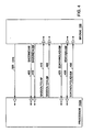
- the method comprises system asserting the reset# signal 310, the connect line 320, and/or the CFR signal 325 (step 905).
- the method also comprises a processor asserting the PROCRDY signal line 330 (step 910).
- the method next includes the system deasserting the reset# signal 310 and/or the connect signal 320 (step 915).
- the processor deasserts the PROCRDY signal 330 (step 920).
- a time delay of one or more system clock periods may optionally occur (step 925).
- the system deasserts the CFR signal 325 (step 930).
- the processor monitors the connect signal 320 for the start bit (step 935).
- An optional time delay of one or more system clock periods may occur (step 940).
- the system transmits the serial SIP stream over the connect signal line 320 (step 945).
- the system next asserts and holds the connect signal line 320 (step 950).
- An optional time delay of one or more system clock periods may occur (step 955).
- the processor asserts the PROCRDY signal 330 (step 960), preferably to indicate that the processor 110A is ready for operation.
- step 910 when the processor asserts the PROCRDY signal 330, that the processor may at this time, in one embodiment, convert from running at the system clock frequency to the processor clock frequency. This changeover preferably occurs as a slow ramp-up in the PLL 225.
- the processor When the processor is operating at the processor frequency, instead of the system clock frequency, the processor will deassert the PROCRDY signal 330 in step 920.
- Fig. 10 a flowchart of an embodiment of a method for initializing source-synchronous clocking between one of the processors and the bridge of Fig. 1 is illustrated. While the processor 110A is operating at the system clock frequency, either RSTCLK 220 or CLKIN 215, transfers between the processor 110A and the bridge 130 are synchronous transfers at the RSTCLK 220 or CLKEND 215 frequency. The method of Fig. 10 converts transfers between the processor 110A and the bridge 130 from synchronous transfers to source-synchronous transfers, also known as clock forwarded transfers.
- the method comprises that after a time delay of one or more system clock periods after the processor asserts PROCRDY 330 in step 960, the system deasserts clock forward reset 325 signal (step 1010).
- the processor samples the CFR signal 325 during the next system clock (step 1020).
- the system drives its source-synchronous clocks to the processor (step 1040).
- the processor drives its source-synchronous clocks to the system concurrently with the system driving its source-synchronous clocks to the processor.
- the start bit and the ratio bit may be embodied as multiple bits. In other words, there may be one or more start bits and one or more ratio bits at the beginning of the SIP stream.
- the SIP receive logic only requires one start bit even if there are multiple ratio bits. If there are multiple ratio bits, additional chains of storage elements are linked between storage element 515 and 525 similar to the way in which storage elements 515, 525, and 535 are linked between storage elements 510 and 520. Thus, when the start bit reaches the last storage element in the chain, the ratio bits may be read from the storage elements at the end of the earlier storage element chains by the control logic 540.
- this last storage element should be clocked on the falling edge of PCLK 230 and enabled by conditional enable signal 550 from control logic 540. It is also noted that multiple start bits may be used to ensure that noise over connect 320 is minimized so that the start of the SIP stream may be recognized.
- the encoding of the one or more start bits and the encoding of the one or more ratio bits may be designed for the appropriate system.
- This invention may be employed in digital electronic systems.
Landscapes
- Engineering & Computer Science (AREA)
- Theoretical Computer Science (AREA)
- General Engineering & Computer Science (AREA)
- Physics & Mathematics (AREA)
- General Physics & Mathematics (AREA)
- Computer Hardware Design (AREA)
- Information Transfer Systems (AREA)
- Synchronisation In Digital Transmission Systems (AREA)
- Power Sources (AREA)
Applications Claiming Priority (3)
| Application Number | Priority Date | Filing Date | Title |
|---|---|---|---|
| US386650 | 1989-07-31 | ||
| US09/386,650 US6393502B1 (en) | 1999-08-31 | 1999-08-31 | System and method for initiating a serial data transfer between two clock domains |
| PCT/US2000/007695 WO2001016773A1 (en) | 1999-08-31 | 2000-03-23 | System and method for initiating a serial data transfer between two clock domains |
Publications (2)
| Publication Number | Publication Date |
|---|---|
| EP1214662A1 EP1214662A1 (en) | 2002-06-19 |
| EP1214662B1 true EP1214662B1 (en) | 2003-05-07 |
Family
ID=23526484
Family Applications (1)
| Application Number | Title | Priority Date | Filing Date |
|---|---|---|---|
| EP00919559A Expired - Lifetime EP1214662B1 (en) | 1999-08-31 | 2000-03-23 | System and method for initiating a serial data transfer between two clock domains |
Country Status (6)
| Country | Link |
|---|---|
| US (3) | US6393502B1 (https=) |
| EP (1) | EP1214662B1 (https=) |
| JP (1) | JP4630512B2 (https=) |
| KR (1) | KR100734528B1 (https=) |
| DE (1) | DE60002589T2 (https=) |
| WO (1) | WO2001016773A1 (https=) |
Families Citing this family (47)
| Publication number | Priority date | Publication date | Assignee | Title |
|---|---|---|---|---|
| JP4091195B2 (ja) * | 1999-02-08 | 2008-05-28 | 富士通株式会社 | インタフェース制御装置及びインタフェース制御方法 |
| US6535565B1 (en) * | 1999-03-16 | 2003-03-18 | Level One Communications, Inc. | Receiver rate converter phase calculation apparatus and method |
| US6584575B1 (en) * | 1999-08-31 | 2003-06-24 | Advanced Micro Devices, Inc. | System and method for initializing source-synchronous data transfers using ratio bits |
| US7039074B1 (en) * | 2000-09-14 | 2006-05-02 | Agiletv Corporation | N-way demultiplexer |
| US7047196B2 (en) | 2000-06-08 | 2006-05-16 | Agiletv Corporation | System and method of voice recognition near a wireline node of a network supporting cable television and/or video delivery |
| KR100369768B1 (ko) | 2000-12-09 | 2003-03-03 | 엘지전자 주식회사 | 휴대용 컴퓨터에서의 버스 클럭 주파수 제어장치 |
| US6715094B2 (en) * | 2000-12-20 | 2004-03-30 | Intel Corporation | Mult-mode I/O interface for synchronizing selected control patterns into control clock domain to obtain interface control signals to be transmitted to I/O buffers |
| US8095370B2 (en) | 2001-02-16 | 2012-01-10 | Agiletv Corporation | Dual compression voice recordation non-repudiation system |
| US6952174B2 (en) * | 2001-09-07 | 2005-10-04 | Microsemi Corporation | Serial data interface |
| US6959398B2 (en) * | 2001-12-31 | 2005-10-25 | Hewlett-Packard Development Company, L.P. | Universal asynchronous boundary module |
| US8219736B2 (en) * | 2002-02-12 | 2012-07-10 | Ati Technologies Ulc | Method and apparatus for a data bridge in a computer system |
| US6898725B2 (en) * | 2002-03-27 | 2005-05-24 | International Business Machines Corporation | Method for adjusting system clocks using dynamic clock ratio detector to detect clock ratio between clock domain of driver and counting receiver clock domain |
| JP4159415B2 (ja) | 2002-08-23 | 2008-10-01 | エルピーダメモリ株式会社 | メモリモジュール及びメモリシステム |
| JP2004112182A (ja) * | 2002-09-17 | 2004-04-08 | Fuji Xerox Co Ltd | 通信端末装置及びその制御方法 |
| US7324589B2 (en) * | 2003-02-05 | 2008-01-29 | Fujitsu Limited | Method and system for providing error compensation to a signal using feedback control |
| US7313210B2 (en) * | 2003-02-28 | 2007-12-25 | Hewlett-Packard Development Company, L.P. | System and method for establishing a known timing relationship between two clock signals |
| US20040193931A1 (en) * | 2003-03-26 | 2004-09-30 | Akkerman Ryan L. | System and method for transferring data from a first clock domain to a second clock domain |
| US7275171B2 (en) * | 2003-05-22 | 2007-09-25 | Rambus Inc. | Method and apparatus for programmable sampling clock edge selection |
| EP1515271A1 (en) * | 2003-09-09 | 2005-03-16 | STMicroelectronics S.r.l. | Method and device for extracting a subset of data from a set of data |
| US7657689B1 (en) * | 2003-10-07 | 2010-02-02 | Altera Corporation | Methods and apparatus for handling reset events in a bus bridge |
| FR2870368B1 (fr) * | 2004-01-27 | 2006-12-15 | Atmel Corp | Procede et dispositif pour piloter de multiples peripheriques avec des frequences d'horloge differentes dans un circuit integre |
| US20060023819A1 (en) * | 2004-07-29 | 2006-02-02 | Adkisson Richard W | Clock synchronizer |
| US7436917B2 (en) * | 2004-07-29 | 2008-10-14 | Hewlett-Packard Development Company, L.P. | Controller for clock synchronizer |
| US8660647B2 (en) * | 2005-07-28 | 2014-02-25 | Cyberonics, Inc. | Stimulating cranial nerve to treat pulmonary disorder |
| US7614737B2 (en) * | 2005-12-16 | 2009-11-10 | Lexmark International Inc. | Method for identifying an installed cartridge |
| KR20070114557A (ko) * | 2006-05-29 | 2007-12-04 | 삼성전자주식회사 | 퓨즈를 갖는 반도체 기억 소자 및 그 형성 방법 |
| US7760798B2 (en) * | 2006-05-30 | 2010-07-20 | Fujitsu Limited | System and method for adjusting compensation applied to a signal |
| US7839958B2 (en) | 2006-05-30 | 2010-11-23 | Fujitsu Limited | System and method for the adjustment of compensation applied to a signal |
| US7817757B2 (en) * | 2006-05-30 | 2010-10-19 | Fujitsu Limited | System and method for independently adjusting multiple offset compensations applied to a signal |
| US7804921B2 (en) | 2006-05-30 | 2010-09-28 | Fujitsu Limited | System and method for decoupling multiple control loops |
| US7848470B2 (en) * | 2006-05-30 | 2010-12-07 | Fujitsu Limited | System and method for asymmetrically adjusting compensation applied to a signal |
| US7839955B2 (en) * | 2006-05-30 | 2010-11-23 | Fujitsu Limited | System and method for the non-linear adjustment of compensation applied to a signal |
| US7764757B2 (en) * | 2006-05-30 | 2010-07-27 | Fujitsu Limited | System and method for the adjustment of offset compensation applied to a signal |
| US7817712B2 (en) * | 2006-05-30 | 2010-10-19 | Fujitsu Limited | System and method for independently adjusting multiple compensations applied to a signal |
| US7804894B2 (en) | 2006-05-30 | 2010-09-28 | Fujitsu Limited | System and method for the adjustment of compensation applied to a signal using filter patterns |
| US7787534B2 (en) * | 2006-05-30 | 2010-08-31 | Fujitsu Limited | System and method for adjusting offset compensation applied to a signal |
| US7801208B2 (en) * | 2006-05-30 | 2010-09-21 | Fujitsu Limited | System and method for adjusting compensation applied to a signal using filter patterns |
| CN101617371B (zh) * | 2007-02-16 | 2014-03-26 | 莫塞德技术公司 | 具有多个外部电源的非易失性半导体存储器 |
| US7466247B1 (en) | 2007-10-04 | 2008-12-16 | Lecroy Corporation | Fractional-decimation signal processing |
| US8781053B2 (en) * | 2007-12-14 | 2014-07-15 | Conversant Intellectual Property Management Incorporated | Clock reproducing and timing method in a system having a plurality of devices |
| US8467486B2 (en) * | 2007-12-14 | 2013-06-18 | Mosaid Technologies Incorporated | Memory controller with flexible data alignment to clock |
| US9197981B2 (en) * | 2011-04-08 | 2015-11-24 | The Regents Of The University Of Michigan | Coordination amongst heterogeneous wireless devices |
| US9858322B2 (en) | 2013-11-11 | 2018-01-02 | Amazon Technologies, Inc. | Data stream ingestion and persistence techniques |
| FR3029661B1 (fr) * | 2014-12-04 | 2016-12-09 | Stmicroelectronics Rousset | Procedes de transmission et de reception d'un signal binaire sur un lien serie, en particulier pour la detection de la vitesse de transmission, et dispositifs correspondants |
| US9825730B1 (en) * | 2016-09-26 | 2017-11-21 | Dell Products, Lp | System and method for optimizing link performance with lanes operating at different speeds |
| DE102019112447A1 (de) * | 2019-05-13 | 2020-11-19 | Jenoptik Optical Systems Gmbh | Verfahren und Auswerteeinheit zur Ermittlung eines Zeitpunkts einer Flanke in einem Signal |
| US11860685B2 (en) | 2021-10-29 | 2024-01-02 | Advanced Micro Devices, Inc. | Clock frequency divider circuit |
Family Cites Families (46)
| Publication number | Priority date | Publication date | Assignee | Title |
|---|---|---|---|---|
| US3725793A (en) | 1971-12-15 | 1973-04-03 | Bell Telephone Labor Inc | Clock synchronization arrangement employing delay devices |
| JPS5911056A (ja) * | 1982-07-09 | 1984-01-20 | Nec Corp | 調歩同期式通信方式 |
| JPS61169956A (ja) * | 1985-01-23 | 1986-07-31 | Fujitsu Ltd | デ−タ転送速度同期方式 |
| DE3643766A1 (de) | 1986-12-20 | 1988-07-07 | Standard Elektrik Lorenz Ag | Datenbussystem fuer einen seriellen datenbus |
| KR900001817B1 (ko) | 1987-08-01 | 1990-03-24 | 삼성전자 주식회사 | 저항 수단을 이용한 씨 모스 티티엘 인푸트 버퍼 |
| JPH07114348B2 (ja) | 1987-12-11 | 1995-12-06 | 日本電気株式会社 | 論理回路 |
| JPH01194548A (ja) * | 1988-01-28 | 1989-08-04 | Fujitsu Ltd | 調歩同期式データ伝送の速度設定方式 |
| JPH07120225B2 (ja) | 1988-04-15 | 1995-12-20 | 富士通株式会社 | 半導体回路装置 |
| US4989175A (en) | 1988-11-25 | 1991-01-29 | Unisys Corp. | High speed on-chip clock phase generating system |
| JP2559237Y2 (ja) * | 1989-01-23 | 1998-01-14 | 旭光学工業株式会社 | シリアルデータサンプリング信号発生装置 |
| JPH02202738A (ja) * | 1989-02-01 | 1990-08-10 | Fujitsu Ltd | シリアルデータ受信回路 |
| US5058132A (en) | 1989-10-26 | 1991-10-15 | National Semiconductor Corporation | Clock distribution system and technique |
| JPH0377543U (https=) * | 1989-11-28 | 1991-08-05 | ||
| US5295257A (en) * | 1991-05-24 | 1994-03-15 | Alliedsignal Inc. | Distributed multiple clock system and a method for the synchronization of a distributed multiple system |
| US5307381A (en) | 1991-12-27 | 1994-04-26 | Intel Corporation | Skew-free clock signal distribution network in a microprocessor |
| GB2265283B (en) * | 1992-03-18 | 1995-10-25 | Crystal Semiconductor Corp | Resynchronization of a synchronous serial interface |
| US5459855A (en) * | 1992-08-10 | 1995-10-17 | Hewlett-Packard Company | Frequency ratio detector for determining fixed frequency ratios in a computer system |
| US5256994A (en) | 1992-09-21 | 1993-10-26 | Intel Corporation | Programmable secondary clock generator |
| CA2124709C (en) * | 1993-08-24 | 1998-06-09 | Lee-Fang Wei | Reduced speed equalizer |
| JP3402498B2 (ja) * | 1993-12-24 | 2003-05-06 | パイオニア株式会社 | 車載用電子機器 |
| US6112307A (en) * | 1993-12-30 | 2000-08-29 | Intel Corporation | Method and apparatus for translating signals between clock domains of different frequencies |
| JP3466738B2 (ja) | 1994-11-21 | 2003-11-17 | ヤマハ株式会社 | 非同期シリアルデータ受信装置 |
| US5550780A (en) * | 1994-12-19 | 1996-08-27 | Cirrus Logic, Inc. | Two cycle asynchronous FIFO queue |
| SE515563C2 (sv) * | 1995-01-11 | 2001-08-27 | Ericsson Telefon Ab L M | Dataöverföringssystem |
| US6169772B1 (en) * | 1995-04-07 | 2001-01-02 | Via-Cyrix, Inc. | Stretching setup and hold times in synchronous designs |
| US5825834A (en) * | 1995-10-13 | 1998-10-20 | Vlsi Technlogy, Inc. | Fast response system implementing a sampling clock for extracting stable clock information from a serial data stream with defined jitter characeristics and method therefor |
| US5859881A (en) * | 1996-06-07 | 1999-01-12 | International Business Machines Corporation | Adaptive filtering method and apparatus to compensate for a frequency difference between two clock sources |
| GB2315197B (en) * | 1996-07-11 | 2000-07-12 | Nokia Mobile Phones Ltd | Method and apparatus for system clock adjustment |
| JP3582238B2 (ja) * | 1996-07-15 | 2004-10-27 | 松下電器産業株式会社 | 信号判定器およびこれを用いた無線装置 |
| US5909563A (en) * | 1996-09-25 | 1999-06-01 | Philips Electronics North America Corporation | Computer system including an interface for transferring data between two clock domains |
| US6055645A (en) * | 1996-12-30 | 2000-04-25 | Intel Corporation | Method and apparatus for providing a clock signal to a processor |
| GB2321351B (en) * | 1997-01-17 | 1999-03-10 | Paul Flood | System and method for data transfer across multiple clock domains |
| US6061410A (en) * | 1997-02-27 | 2000-05-09 | Advanced Micro Devices | Frequency ratio estimation arrangement and method thereof |
| US6202108B1 (en) * | 1997-03-13 | 2001-03-13 | Bull S.A. | Process and system for initializing a serial link between two integrated circuits comprising a parallel-serial port using two clocks with different frequencies |
| KR100230451B1 (ko) * | 1997-04-08 | 1999-11-15 | 윤종용 | 디지털 신호처리 프로세서의 비동기방식 직렬데이터 송수신 방법 |
| JPH10322404A (ja) * | 1997-05-19 | 1998-12-04 | Sharp Corp | シリアルデータ通信方法および装置 |
| FR2764758B1 (fr) * | 1997-06-12 | 1999-08-06 | Scm Schneider Microsysteme Mic | Procede de mesure automatique de l'unite de temps pour peripheriques de communication dedies aux cartes a puce |
| US6249555B1 (en) * | 1997-07-14 | 2001-06-19 | Grass Valley (Us) Inc. | Low jitter digital extraction of data from serial bitstreams |
| US6000022A (en) * | 1997-10-10 | 1999-12-07 | Micron Technology, Inc. | Method and apparatus for coupling signals between two circuits operating in different clock domains |
| US6269136B1 (en) * | 1998-02-02 | 2001-07-31 | Microunity Systems Engineering, Inc. | Digital differential analyzer data synchronizer |
| US6260152B1 (en) * | 1998-07-30 | 2001-07-10 | Siemens Information And Communication Networks, Inc. | Method and apparatus for synchronizing data transfers in a logic circuit having plural clock domains |
| US6128678A (en) * | 1998-08-28 | 2000-10-03 | Theseus Logic, Inc. | FIFO using asynchronous logic to interface between clocked logic circuits |
| US6000107A (en) * | 1998-09-15 | 1999-12-14 | West; Stephen W. | Fastening device |
| US6321342B1 (en) * | 1999-03-23 | 2001-11-20 | Lsi Logic Corporation | Method and apparatus for interfacing circuits that operate based upon different clock signals |
| US6172540B1 (en) * | 1999-08-16 | 2001-01-09 | Intel Corporation | Apparatus for fast logic transfer of data across asynchronous clock domains |
| US6327207B1 (en) * | 2001-04-09 | 2001-12-04 | Lsi Logic Corporation | Synchronizing data operations across a synchronization boundary between different clock domains using two-hot encoding |
-
1999
- 1999-08-31 US US09/386,650 patent/US6393502B1/en not_active Expired - Lifetime
- 1999-10-27 US US09/428,633 patent/US6505261B1/en not_active Expired - Lifetime
-
2000
- 2000-03-23 EP EP00919559A patent/EP1214662B1/en not_active Expired - Lifetime
- 2000-03-23 KR KR1020027002343A patent/KR100734528B1/ko not_active Expired - Fee Related
- 2000-03-23 DE DE60002589T patent/DE60002589T2/de not_active Expired - Lifetime
- 2000-03-23 WO PCT/US2000/007695 patent/WO2001016773A1/en not_active Ceased
- 2000-03-23 JP JP2001520658A patent/JP4630512B2/ja not_active Expired - Fee Related
-
2002
- 2002-03-11 US US10/095,019 patent/US6668292B2/en not_active Expired - Lifetime
Also Published As
| Publication number | Publication date |
|---|---|
| US6505261B1 (en) | 2003-01-07 |
| KR100734528B1 (ko) | 2007-07-03 |
| KR20020064277A (ko) | 2002-08-07 |
| DE60002589T2 (de) | 2004-03-25 |
| WO2001016773A1 (en) | 2001-03-08 |
| EP1214662A1 (en) | 2002-06-19 |
| JP4630512B2 (ja) | 2011-02-09 |
| DE60002589D1 (de) | 2003-06-12 |
| US6393502B1 (en) | 2002-05-21 |
| US6668292B2 (en) | 2003-12-23 |
| US20020090046A1 (en) | 2002-07-11 |
| JP2003508956A (ja) | 2003-03-04 |
Similar Documents
| Publication | Publication Date | Title |
|---|---|---|
| EP1214662B1 (en) | System and method for initiating a serial data transfer between two clock domains | |
| US6108729A (en) | Serial bus system for shadowing registers | |
| US5732250A (en) | Multi-function microprocessor wait state mechanism using external control line | |
| EP1027786B1 (en) | Bidirectional communication port for digital signal processor | |
| JPH07306827A (ja) | P/q整数比関係を有する周波数で動作するディジタル装置間で同期データ伝送を行うための方法および装置 | |
| US5519872A (en) | Fast address latch with automatic address incrementing | |
| CA2119200C (en) | Burst srams for use with a high speed clock | |
| US5777500A (en) | Multiple clock source generation with independently adjustable duty cycles | |
| US6434650B1 (en) | Apparatus and method for multiplexing bi-directional data onto a low pin count bus between a host CPU and co-processor | |
| US20050055489A1 (en) | Bridge circuit for use in retiming in a semiconductor integrated circuit | |
| US5978869A (en) | Enhanced dual speed bus computer system | |
| US6535968B2 (en) | Apparatus, system, and method for reducing bus contention during consecutive read-write operations | |
| US6067590A (en) | Data bus agent including a storage medium between a data bus and the bus agent device | |
| KR20050085553A (ko) | 데이터 버스 전력 제어 장치 및 방법 | |
| US7386750B2 (en) | Reduced bus turnaround time in a multiprocessor architecture | |
| US6584575B1 (en) | System and method for initializing source-synchronous data transfers using ratio bits | |
| US6438627B1 (en) | Lower address line prediction and substitution | |
| US6748513B1 (en) | Method and apparatus for a low latency source-synchronous address receiver for a host system bus in a memory controller | |
| US6557064B1 (en) | Set up time adjust | |
| US6275883B1 (en) | Contention-free signaling scheme for shared control signals | |
| US5983300A (en) | Dynamic window mechanism for preventing invalid information propagation from the PCI bus | |
| US6651127B2 (en) | Method of detecting termination of a bus transfer operation | |
| US7519755B2 (en) | Combined command and response on-chip data interface for a computer system chipset | |
| US6026453A (en) | System for facilitating serial data communications utilizing number of cycles input signal remained asserted to indicate data output logical state | |
| US7065669B2 (en) | System and method for providing a write strobe signal to a receiving element before both an address and data signal |
Legal Events
| Date | Code | Title | Description |
|---|---|---|---|
| PUAI | Public reference made under article 153(3) epc to a published international application that has entered the european phase |
Free format text: ORIGINAL CODE: 0009012 |
|
| 17P | Request for examination filed |
Effective date: 20020116 |
|
| AK | Designated contracting states |
Kind code of ref document: A1 Designated state(s): AT BE CH CY DE DK ES FI FR GB GR IE IT LI LU MC NL PT SE |
|
| GRAH | Despatch of communication of intention to grant a patent |
Free format text: ORIGINAL CODE: EPIDOS IGRA |
|
| GRAH | Despatch of communication of intention to grant a patent |
Free format text: ORIGINAL CODE: EPIDOS IGRA |
|
| GRAA | (expected) grant |
Free format text: ORIGINAL CODE: 0009210 |
|
| AK | Designated contracting states |
Designated state(s): DE GB |
|
| REG | Reference to a national code |
Ref country code: GB Ref legal event code: FG4D |
|
| REG | Reference to a national code |
Ref country code: IE Ref legal event code: FG4D |
|
| REF | Corresponds to: |
Ref document number: 60002589 Country of ref document: DE Date of ref document: 20030612 Kind code of ref document: P |
|
| PLBE | No opposition filed within time limit |
Free format text: ORIGINAL CODE: 0009261 |
|
| STAA | Information on the status of an ep patent application or granted ep patent |
Free format text: STATUS: NO OPPOSITION FILED WITHIN TIME LIMIT |
|
| 26N | No opposition filed |
Effective date: 20040210 |
|
| REG | Reference to a national code |
Ref country code: IE Ref legal event code: MM4A |
|
| REG | Reference to a national code |
Ref country code: GB Ref legal event code: 732E Free format text: REGISTERED BETWEEN 20091210 AND 20091216 |
|
| PGFP | Annual fee paid to national office [announced via postgrant information from national office to epo] |
Ref country code: GB Payment date: 20100208 Year of fee payment: 11 |
|
| PGFP | Annual fee paid to national office [announced via postgrant information from national office to epo] |
Ref country code: DE Payment date: 20110331 Year of fee payment: 12 |
|
| GBPC | Gb: european patent ceased through non-payment of renewal fee |
Effective date: 20110323 |
|
| PG25 | Lapsed in a contracting state [announced via postgrant information from national office to epo] |
Ref country code: GB Free format text: LAPSE BECAUSE OF NON-PAYMENT OF DUE FEES Effective date: 20110323 |
|
| REG | Reference to a national code |
Ref country code: DE Ref legal event code: R119 Ref document number: 60002589 Country of ref document: DE Effective date: 20121002 |
|
| PG25 | Lapsed in a contracting state [announced via postgrant information from national office to epo] |
Ref country code: DE Free format text: LAPSE BECAUSE OF NON-PAYMENT OF DUE FEES Effective date: 20121002 |