EP1200967B1 - Multilayer optics with adjustable working wavelength - Google Patents
Multilayer optics with adjustable working wavelength Download PDFInfo
- Publication number
- EP1200967B1 EP1200967B1 EP00952405A EP00952405A EP1200967B1 EP 1200967 B1 EP1200967 B1 EP 1200967B1 EP 00952405 A EP00952405 A EP 00952405A EP 00952405 A EP00952405 A EP 00952405A EP 1200967 B1 EP1200967 B1 EP 1200967B1
- Authority
- EP
- European Patent Office
- Prior art keywords
- reflector
- spacing
- multilayer
- electromagnetic
- curvature
- Prior art date
- Legal status (The legal status is an assumption and is not a legal conclusion. Google has not performed a legal analysis and makes no representation as to the accuracy of the status listed.)
- Expired - Lifetime
Links
- 239000000758 substrate Substances 0.000 claims description 2
- 230000005855 radiation Effects 0.000 description 7
- 230000003287 optical effect Effects 0.000 description 3
- PXHVJJICTQNCMI-UHFFFAOYSA-N Nickel Chemical compound [Ni] PXHVJJICTQNCMI-UHFFFAOYSA-N 0.000 description 2
- 239000013078 crystal Substances 0.000 description 2
- 230000001419 dependent effect Effects 0.000 description 2
- 238000010586 diagram Methods 0.000 description 2
- BASFCYQUMIYNBI-UHFFFAOYSA-N platinum Chemical compound [Pt] BASFCYQUMIYNBI-UHFFFAOYSA-N 0.000 description 2
- OKTJSMMVPCPJKN-UHFFFAOYSA-N Carbon Chemical compound [C] OKTJSMMVPCPJKN-UHFFFAOYSA-N 0.000 description 1
- RYGMFSIKBFXOCR-UHFFFAOYSA-N Copper Chemical compound [Cu] RYGMFSIKBFXOCR-UHFFFAOYSA-N 0.000 description 1
- 238000002441 X-ray diffraction Methods 0.000 description 1
- 238000000441 X-ray spectroscopy Methods 0.000 description 1
- 238000010521 absorption reaction Methods 0.000 description 1
- 239000011248 coating agent Substances 0.000 description 1
- 238000000576 coating method Methods 0.000 description 1
- 238000010276 construction Methods 0.000 description 1
- 229910052802 copper Inorganic materials 0.000 description 1
- 239000010949 copper Substances 0.000 description 1
- 238000011161 development Methods 0.000 description 1
- 230000018109 developmental process Effects 0.000 description 1
- 230000000694 effects Effects 0.000 description 1
- PCHJSUWPFVWCPO-UHFFFAOYSA-N gold Chemical compound [Au] PCHJSUWPFVWCPO-UHFFFAOYSA-N 0.000 description 1
- 229910052737 gold Inorganic materials 0.000 description 1
- 239000010931 gold Substances 0.000 description 1
- 229910002804 graphite Inorganic materials 0.000 description 1
- 239000010439 graphite Substances 0.000 description 1
- 239000000463 material Substances 0.000 description 1
- 238000005259 measurement Methods 0.000 description 1
- 238000000034 method Methods 0.000 description 1
- 238000012986 modification Methods 0.000 description 1
- 230000004048 modification Effects 0.000 description 1
- 229910052759 nickel Inorganic materials 0.000 description 1
- 229910052697 platinum Inorganic materials 0.000 description 1
- 238000013519 translation Methods 0.000 description 1
Images


Classifications
-
- G—PHYSICS
- G02—OPTICS
- G02B—OPTICAL ELEMENTS, SYSTEMS OR APPARATUS
- G02B5/00—Optical elements other than lenses
- G02B5/08—Mirrors
- G02B5/0883—Mirrors with a refractive index gradient
-
- B—PERFORMING OPERATIONS; TRANSPORTING
- B82—NANOTECHNOLOGY
- B82Y—SPECIFIC USES OR APPLICATIONS OF NANOSTRUCTURES; MEASUREMENT OR ANALYSIS OF NANOSTRUCTURES; MANUFACTURE OR TREATMENT OF NANOSTRUCTURES
- B82Y10/00—Nanotechnology for information processing, storage or transmission, e.g. quantum computing or single electron logic
-
- G—PHYSICS
- G02—OPTICS
- G02B—OPTICAL ELEMENTS, SYSTEMS OR APPARATUS
- G02B5/00—Optical elements other than lenses
- G02B5/08—Mirrors
- G02B5/0891—Ultraviolet [UV] mirrors
-
- G—PHYSICS
- G21—NUCLEAR PHYSICS; NUCLEAR ENGINEERING
- G21K—TECHNIQUES FOR HANDLING PARTICLES OR IONISING RADIATION NOT OTHERWISE PROVIDED FOR; IRRADIATION DEVICES; GAMMA RAY OR X-RAY MICROSCOPES
- G21K1/00—Arrangements for handling particles or ionising radiation, e.g. focusing or moderating
- G21K1/06—Arrangements for handling particles or ionising radiation, e.g. focusing or moderating using diffraction, refraction or reflection, e.g. monochromators
- G21K1/062—Devices having a multilayer structure
-
- G—PHYSICS
- G21—NUCLEAR PHYSICS; NUCLEAR ENGINEERING
- G21K—TECHNIQUES FOR HANDLING PARTICLES OR IONISING RADIATION NOT OTHERWISE PROVIDED FOR; IRRADIATION DEVICES; GAMMA RAY OR X-RAY MICROSCOPES
- G21K2201/00—Arrangements for handling radiation or particles
- G21K2201/06—Arrangements for handling radiation or particles using diffractive, refractive or reflecting elements
- G21K2201/061—Arrangements for handling radiation or particles using diffractive, refractive or reflecting elements characterised by a multilayer structure
-
- G—PHYSICS
- G21—NUCLEAR PHYSICS; NUCLEAR ENGINEERING
- G21K—TECHNIQUES FOR HANDLING PARTICLES OR IONISING RADIATION NOT OTHERWISE PROVIDED FOR; IRRADIATION DEVICES; GAMMA RAY OR X-RAY MICROSCOPES
- G21K2201/00—Arrangements for handling radiation or particles
- G21K2201/06—Arrangements for handling radiation or particles using diffractive, refractive or reflecting elements
- G21K2201/067—Construction details
Definitions
- the present invention relates to an electromagnetic reflector for reflecting electromagnetic waves. More specifically the present invention relates to reflective multilayer x-ray optics having adjustable working wavelengths.
- X-ray optics are used in many applications such as x-ray diffraction analysis and spectroscopy that require the directing, focusing, collimation, or monochromatizing of x-ray energy from an x-ray source.
- the family of x-ray optics or reflectors used in such applications presently include: total reflection mirrors having a reflective surface coated with gold, copper, nickel, platinum, and other similar elements; crystal diffraction elements such as graphite; and multilayer structures.
- the reflective surfaces in the present invention are configured as multilayer or graded-d multilayer x-ray reflective surfaces.
- Multilayer or graded-d multilayer reflectors/mirrors are optics which utilize their inherent multilayer structure to reflect narrow band or monochromatic x-ray radiation.
- the multilayer structure of the present invention comprises light element layers of relatively low electron density alternating with heavy element layers of relatively high electron density, both of which define the d-spacing of the multilayer.
- the bandwidth of the reflected x-ray radiation can be customized by manipulating the optical and multilayer parameters of the reflector.
- the d spacing may be changed depthwise to control the bandpass of the multilayer mirror.
- the d-spacing of a multilayer mirror can also be tailored through lateral grading in such a way that the Bragg condition is satisfied at every point on a curved multilayer reflector.
- Curved multilayer reflectors including parabolic, elliptical, and other aspherically shaped reflectors must satisfy Bragg's law to reflect a certain specific x-ray wavelength (also referred to as energy or frequency). Bragg's law must be satisfied at every point on a curvature for a defined contour of such a reflecting mirror. Different reflecting surfaces require different d-spacing to reflect a specific x-ray wavelength. This means the d-spacing should be matched with the curvature of a reflector to satisfy Bragg's law such that the desired x-ray wavelength will be reflected. Since Bragg's law must be satisfied, the incident angle and d-spacing are normally fixed and thus the reflected or working wavelength is fixed.
- the US-A-5 825 844 discloses an electromagnetic reflector comprising a multilayer structure the curvature of which may be varied by a movement apparatus to reflect multiple electromagnetic frequencies.
- the US-A-4 958 363 discloses an electromagnetic reflector comprising a multilayer structure having a d-spacing to reflect multiple electromagnetic frequencies.
- the present invention provides for an electromagnetic reflector as defined in claim 1.
- Advantageous developments of the invention are defined in the dependent claims.
- FIG. 1 is a cross-sectional diagrammatic view of a multilayer reflector 10.
- the multilayer reflector 10 is deposited on a substrate 12 and comprises a plurality of layer sets with a thickness d.
- Each layer set 14 is made up of two separate layers of different materials; one with a relatively high electron density and one with a relatively low electron density.
- x-ray radiation 13 is incident on the multilayer reflector 10 and narrow band or generally monochromatic radiation 16 is reflected according to Bragg's law.
- Figure 2 is a cross sectional diagram of a multilayer structure 18 having a plurality of distinct d-spacings d1 and d2 varying in the depth direction and defined as depth grading.
- the multilayer structure 18 because of the distinct d-spacings d1 and d2 may reflect multiple x-ray wavelengths (i.e. different groups of d-spacing to satisfy a discrete range of reflected wavelengths).
- polychromatic x-ray radiation 20 is incident on the surface of the multilayer structure 18 and low energy x-rays 22 are reflected by the relatively thicker d-spacings d2 and high energy x-rays 24 are reflected by the relatively thinner d-spacings d1.
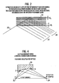
- Figures 3 and 4 are cross-sectional diagrams of fixed curvature multilayer optics 26 and 28 which generally reflect only one x-ray wavelength.
- Figure 3 illustrates the parabolically shaped multilayer optic 26 which collimates x-ray beams generated by an idealized point x-ray source 30 and
- Figure 4 illustrates the elliptically shaped multilayer optic 28 which focuses x-ray beams generated by an x-ray source 32 to a focal point 34.
- the curvature and d-spacing of optics 26 and 28 have been permanently configured to satisfy Bragg's law for a specific wavelength at every point on the surface of the optics 26 and 28.
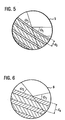
- Figures 5, 6, 7, and 8 are cross-sectional magnified views of the multilayer surfaces taken within circles 5, 6, 7, and 8 of Figures 3 and 4. From these figures the variation in incident angle and the lateral grading of the d-spacing in order to satisfy Bragg's law for a specific frequency can be seen.
- the parabolic optic 26 includes incident angle ⁇ 1 and d-spacing d3 at one area of its surface and incident angle ⁇ 2 and d-spacing d4 at another area. While these parameters are different, the result is that these areas reflect generally the same x-ray wavelength following Bragg's law.
- the elliptical optic 28 includes incident angle ⁇ 3 and d-spacing d5 at one area of its surface and incident angle ⁇ 4 and d-spacing d6 at another area which reflect the same x-ray wavelength.
- the shortcomings with these type of fixed curvature reflectors is that they may only be used to reflect a single x-ray wavelength or narrow band.
- multilayer reflectors require different d-spacing variations to reflect different x-ray wavelengths at the same incident angle and the d-spacing should match the surface curvature (angle of incidence) to reflect x-rays according to Bragg's law.
- the present invention provides electromagnetic reflectors which may be used to reflect a plurality of x-ray wavelengths having substantially no overlap.
- a first embodiment of the present invention shown by Figure 8 comprises a multilayer reflector with variable curvature and a laterally graded d-spacing. If a multilayer is a flat reflector with uniform d-spacing, the flat reflector can be rotated to reflect x-rays of different wavelengths, as the incidence angle will vary. If a multilayer has a curved surface the d-spacing must be laterally graded to satisfy Bragg's law at every point. Thus, the d-spacing or incidence angle may be changed to vary the x-ray wavelength reflected from a multilayer reflector.
- the laterally graded d-spacing of a multilayer reflector may remain constant while only the curvature is varied and the curvature of a multilayer reflector may remain constant and have multiple graded d-spacings such that multiple x-ray wavelengths may be reflected by the multilayer reflector.
- either the d-spacing variation of the multilayer coating or the curvature of the optics can be manipulated such that the multilayer optics reflect x-rays with different wavelengths.
- the sin ⁇ can be written, at a very accurate approximation, as a product of a factor "C" (an arbitrary constant) and common form which is independent from the x-ray energy.
- the same d-spacing can be used for different wavelengths by changing the factor C such that ⁇ /C is a constant.
- y 2 px
- p the parabolic parameter.
- d-spacing can be maintained for different reflected wavelengths by altering the curvature or parabolic parameter (p) of a parabolic shaped multilayer reflector.
- x and y are points in a Cartesian coordinate system and a is the major radius of the ellipse and b is the minor radius of the ellipse.
- the minor radius is much smaller than the major radius.
- d-spacing is defined as well as the wavelength dependency on d-spacing for a multilayer reflector.
- the "real d-spacing", or the “geometric d-spacing is different from the "first order Bragg d-spacing” due to the effects of refraction in the multilayer structure.
- a multilayer optic is used as a first order Bragg reflector. This,is the reason that "d-spacing" is commonly defined and measured by the first order Bragg's law.
- Such defined d-spacing is the same for different wavelengths as shown in the following discussion.
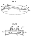
- a variable curvature multilayer reflector 36 is shown in two positions 38 and 40 having two different curvatures defined by the ellipses 33 and 35 and reflecting different x-ray wavelengths 39 and 41 to a focal point 31.
- a similar scheme may be configured for parabolic collimating mirrors which conform to two different parabolas.
- the reflector 36 has more curvature at position 38 then at position 40. The increased curvature will allow the reflector to reflect larger x-ray wavelengths at position 38 then at position 40.
- the reflector at position 40 is modified with less curvature then at position 38 and will reflect shorter x-ray wavelengths.
- the curvature of the reflector 36 is exaggerated in Figure 9 to help illustrate the curvature at the alternate positions 38 and 40.
- the minor radius b ⁇ a C (10)
- the manipulation of the parabolic parameter p of the parabolic reflector and the minor radius b of the elliptical reflector may be adjusted to vary the wavelength of the reflected x-rays.
- a four point bender 42 is shown in Figure 10 having precision actuators 44a and 44b which will vary the curvature of the reflector 36. Posts 43a-b are fixed while members 45a-b are actuated to alter the curvature of the reflector 36.
- the bender 42 will vary the parabolic parameter p of a parabolically shaped multilayer reflector and the minor radius b of an elliptically shaped multilayer reflector as detailed above.
- a multilayer reflector 46 of fixed curvature with a plurality of distinct d-spacings d7 and d8, is configured to reflect multiple x-ray wavelengths.
- Each d-spacing d7 and d8 will satisfy Bragg's law for a specific x-ray wavelength.
- the relatively larger d-spacing d8 will reflect longer wavelengths and the relatively shorter d-spacing d7 will reflect shorter wavelengths.
- the reflected wavelengths will have substantially no overlap. Since the absorption for lower energy (longer wavelength) x-rays is stronger, the reflection layer d8 for the lower energy x-rays should be the top layers on the reflector 46.
- the d-spacings d7 and d8 are laterally graded in cooperation with the curvature of the reflector 46 to satisfy Bragg's law for a plurality of specific x-ray wavelengths.
- additional groups of d-spacings may be used limited only by the dimensions and structure of the reflector 46.
- a multilayer reflector 48 having stripe like sections 50 with different d-spacings is shown.
- Each stripe 50 has a d-spacing configured to reflect specific x-ray wavelengths.
- An x-ray source 52 needs only to be translated relative to the stripe like sections 50 of the reflector 48 to change the wavelength of the x-rays reflected from the reflector 48.
- the preferred method of translation is to fix the position of the x-ray source 52 while translating the reflector 48.
Landscapes
- Physics & Mathematics (AREA)
- Engineering & Computer Science (AREA)
- Chemical & Material Sciences (AREA)
- Nanotechnology (AREA)
- General Physics & Mathematics (AREA)
- Optics & Photonics (AREA)
- Crystallography & Structural Chemistry (AREA)
- Theoretical Computer Science (AREA)
- High Energy & Nuclear Physics (AREA)
- General Engineering & Computer Science (AREA)
- Spectroscopy & Molecular Physics (AREA)
- Mathematical Physics (AREA)
- Optical Elements Other Than Lenses (AREA)
- Analysing Materials By The Use Of Radiation (AREA)
- Aerials With Secondary Devices (AREA)
- Spectrometry And Color Measurement (AREA)
- Investigating Or Analysing Materials By Optical Means (AREA)
- Semiconductor Lasers (AREA)
- Mechanical Light Control Or Optical Switches (AREA)
- Optical Filters (AREA)
Applications Claiming Priority (3)
| Application Number | Priority Date | Filing Date | Title |
|---|---|---|---|
| US09/366,028 US6421417B1 (en) | 1999-08-02 | 1999-08-02 | Multilayer optics with adjustable working wavelength |
| US366028 | 1999-08-02 | ||
| PCT/US2000/021060 WO2001009904A2 (en) | 1999-08-02 | 2000-08-01 | Multilayer optics with adjustable working wavelength |
Publications (2)
| Publication Number | Publication Date |
|---|---|
| EP1200967A2 EP1200967A2 (en) | 2002-05-02 |
| EP1200967B1 true EP1200967B1 (en) | 2004-10-27 |
Family
ID=23441383
Family Applications (1)
| Application Number | Title | Priority Date | Filing Date |
|---|---|---|---|
| EP00952405A Expired - Lifetime EP1200967B1 (en) | 1999-08-02 | 2000-08-01 | Multilayer optics with adjustable working wavelength |
Country Status (9)
| Country | Link |
|---|---|
| US (1) | US6421417B1 (enExample) |
| EP (1) | EP1200967B1 (enExample) |
| JP (1) | JP2003506732A (enExample) |
| AT (1) | ATE280993T1 (enExample) |
| AU (1) | AU6511100A (enExample) |
| CA (2) | CA2642736A1 (enExample) |
| CZ (1) | CZ301738B6 (enExample) |
| DE (1) | DE60015346T2 (enExample) |
| WO (1) | WO2001009904A2 (enExample) |
Families Citing this family (42)
| Publication number | Priority date | Publication date | Assignee | Title |
|---|---|---|---|---|
| US6870896B2 (en) | 2000-12-28 | 2005-03-22 | Osmic, Inc. | Dark-field phase contrast imaging |
| US6804324B2 (en) * | 2001-03-01 | 2004-10-12 | Osmo, Inc. | X-ray phase contrast imaging using a fabry-perot interferometer concept |
| JP4657506B2 (ja) * | 2001-06-27 | 2011-03-23 | 株式会社リガク | X線分光方法及びx線分光装置 |
| US6510200B1 (en) | 2001-06-29 | 2003-01-21 | Osmic, Inc. | Multi-layer structure with variable bandpass for monochromatization and spectroscopy |
| US6643353B2 (en) | 2002-01-10 | 2003-11-04 | Osmic, Inc. | Protective layer for multilayers exposed to x-rays |
| JP3629520B2 (ja) * | 2002-03-05 | 2005-03-16 | 理学電機工業株式会社 | X線分光素子およびそれを用いた蛍光x線分析装置 |
| JP2003255089A (ja) * | 2002-03-05 | 2003-09-10 | Rigaku Industrial Co | X線分光素子およびそれを用いた蛍光x線分析装置 |
| US6917667B2 (en) * | 2002-09-03 | 2005-07-12 | Rigaku Corporation | Method and apparatus for making parallel X-ray beam and X-ray diffraction apparatus |
| DE10254026C5 (de) * | 2002-11-20 | 2009-01-29 | Incoatec Gmbh | Reflektor für Röntgenstrahlung |
| EP1642304B1 (en) | 2003-06-13 | 2008-03-19 | Osmic, Inc. | Beam conditioning system |
| US7280634B2 (en) | 2003-06-13 | 2007-10-09 | Osmic, Inc. | Beam conditioning system with sequential optic |
| WO2006014376A1 (en) * | 2004-07-02 | 2006-02-09 | The Government Of The United States Of America, As Represented By The Secretary Of The Navy Naval Research Laboratory | Deformable mirror apparatus |
| JP4432822B2 (ja) * | 2005-04-19 | 2010-03-17 | 船井電機株式会社 | 形状可変ミラー及びそれを備えた光ピックアップ装置 |
| US7425193B2 (en) * | 2005-04-21 | 2008-09-16 | Michigan State University | Tomographic imaging system using a conformable mirror |
| DE102006015933B3 (de) * | 2006-04-05 | 2007-10-31 | Incoatec Gmbh | Vorrichtung und Verfahren zum Justieren eines optischen Elements |
| JP4278108B2 (ja) * | 2006-07-07 | 2009-06-10 | 株式会社リガク | 超小角x線散乱測定装置 |
| US7555098B2 (en) * | 2007-05-02 | 2009-06-30 | HD Technologies Inc. | Method and apparatus for X-ray fluorescence analysis and detection |
| US7920676B2 (en) * | 2007-05-04 | 2011-04-05 | Xradia, Inc. | CD-GISAXS system and method |
| US8130902B2 (en) * | 2007-07-31 | 2012-03-06 | Uchicago Argonne, Llc | High-resolution, active-optic X-ray fluorescence analyzer |
| DE102007048743B4 (de) * | 2007-10-08 | 2010-06-24 | Ifg - Institute For Scientific Instruments Gmbh | Verfahren und Vorrichtung zur Bestimmung der energetischen Zusammensetzung von elektromagnetischen Wellen |
| CA2709216C (en) * | 2008-01-30 | 2013-07-02 | Reflective X-Ray Optics Llc | Mirror mounting, alignment, and scanning mechanism and scanning method for radiographic x-ray imaging, and x-ray imaging device having same |
| US7848483B2 (en) * | 2008-03-07 | 2010-12-07 | Rigaku Innovative Technologies | Magnesium silicide-based multilayer x-ray fluorescence analyzers |
| US8126117B2 (en) * | 2010-02-03 | 2012-02-28 | Rigaku Innovative Technologies, Inc. | Multi-beam X-ray system |
| JP4974391B2 (ja) * | 2010-02-21 | 2012-07-11 | 株式会社リガク | X線分光方法及びx線分光装置 |
| US8406374B2 (en) | 2010-06-25 | 2013-03-26 | Rigaku Innovative Technologies, Inc. | X-ray optical systems with adjustable convergence and focal spot size |
| EP2606490B1 (en) | 2010-08-19 | 2018-06-27 | Convergent R.N.R Ltd | System for x-ray irradiation of target volume |
| CN102525492A (zh) * | 2010-12-31 | 2012-07-04 | 上海西门子医疗器械有限公司 | 一种x射线能谱选择装置 |
| KR101332502B1 (ko) * | 2011-06-14 | 2013-11-26 | 전남대학교산학협력단 | 국부적 방사선 치료용 x―선 바늘 모듈 |
| CN103137233A (zh) * | 2011-12-02 | 2013-06-05 | 佳能株式会社 | X射线波导和x射线波导系统 |
| EP2926124B1 (de) * | 2012-11-29 | 2019-01-09 | Helmut Fischer GmbH | Verfahren und vorrichtung zur durchführung einer röntgenfluoreszenzanalyse |
| US10295485B2 (en) | 2013-12-05 | 2019-05-21 | Sigray, Inc. | X-ray transmission spectrometer system |
| USRE48612E1 (en) | 2013-10-31 | 2021-06-29 | Sigray, Inc. | X-ray interferometric imaging system |
| JP6025211B2 (ja) * | 2013-11-28 | 2016-11-16 | 株式会社リガク | X線トポグラフィ装置 |
| CN107847200B (zh) * | 2015-07-14 | 2022-04-01 | 皇家飞利浦有限公司 | 利用增强的x射线辐射的成像装置和系统 |
| DE102017202802A1 (de) * | 2017-02-21 | 2018-08-23 | Carl Zeiss Smt Gmbh | Objektiv und optisches System mit einem solchen Objektiv |
| US10845491B2 (en) | 2018-06-04 | 2020-11-24 | Sigray, Inc. | Energy-resolving x-ray detection system |
| CN112470245B (zh) | 2018-07-26 | 2025-03-18 | 斯格瑞公司 | 高亮度x射线反射源 |
| EP3603516A1 (de) * | 2018-08-02 | 2020-02-05 | Siemens Healthcare GmbH | Röntgenvorrichtung und verfahren zum betrieb der röntgenvorrichtung |
| CN112638261B (zh) | 2018-09-04 | 2025-06-27 | 斯格瑞公司 | 利用滤波的x射线荧光的系统和方法 |
| WO2020051221A2 (en) | 2018-09-07 | 2020-03-12 | Sigray, Inc. | System and method for depth-selectable x-ray analysis |
| CN109799612B (zh) * | 2019-03-15 | 2020-03-31 | 重庆大学 | 曲面反射镜制造方法及变曲率半径点光源线聚焦成像系统 |
| US11217357B2 (en) | 2020-02-10 | 2022-01-04 | Sigray, Inc. | X-ray mirror optics with multiple hyperboloidal/hyperbolic surface profiles |
Family Cites Families (35)
| Publication number | Priority date | Publication date | Assignee | Title |
|---|---|---|---|---|
| US4693933A (en) | 1983-06-06 | 1987-09-15 | Ovonic Synthetic Materials Company, Inc. | X-ray dispersive and reflective structures and method of making the structures |
| US4727000A (en) | 1983-06-06 | 1988-02-23 | Ovonic Synthetic Materials Co., Inc. | X-ray dispersive and reflective structures |
| US4717632A (en) | 1983-08-22 | 1988-01-05 | Ovonic Synthetic-Materials Company, Inc. | Adhesion and composite wear resistant coating and method |
| US4716083A (en) | 1983-09-23 | 1987-12-29 | Ovonic Synthetic Materials Company | Disordered coating |
| US4525853A (en) | 1983-10-17 | 1985-06-25 | Energy Conversion Devices, Inc. | Point source X-ray focusing device |
| US4785470A (en) | 1983-10-31 | 1988-11-15 | Ovonic Synthetic Materials Company, Inc. | Reflectivity and resolution X-ray dispersive and reflective structures for carbon, beryllium and boron analysis |
| US4643951A (en) | 1984-07-02 | 1987-02-17 | Ovonic Synthetic Materials Company, Inc. | Multilayer protective coating and method |
| US4724169A (en) | 1984-10-09 | 1988-02-09 | Ovonic Synthetic Materials Company, Inc. | Method of producing multilayer coatings on a substrate |
| US4675889A (en) | 1985-07-08 | 1987-06-23 | Ovonic Synthetic Materials Company, Inc. | Multiple wavelength X-ray dispersive devices and method of making the devices |
| US4958363A (en) | 1986-08-15 | 1990-09-18 | Nelson Robert S | Apparatus for narrow bandwidth and multiple energy x-ray imaging |
| US4969175A (en) * | 1986-08-15 | 1990-11-06 | Nelson Robert S | Apparatus for narrow bandwidth and multiple energy x-ray imaging |
| US4777090A (en) | 1986-11-03 | 1988-10-11 | Ovonic Synthetic Materials Company | Coated article and method of manufacturing the article |
| US4783374A (en) | 1987-11-16 | 1988-11-08 | Ovonic Synthetic Materials Company | Coated article and method of manufacturing the article |
| WO1989008920A1 (en) | 1988-03-11 | 1989-09-21 | Rosser Roy J | Optical devices and methods of fabrication thereof |
| US4867785A (en) | 1988-05-09 | 1989-09-19 | Ovonic Synthetic Materials Company, Inc. | Method of forming alloy particulates having controlled submicron crystallite size distributions |
| JP2569447B2 (ja) * | 1988-11-28 | 1997-01-08 | 株式会社ニコン | 多層膜反射鏡の製造方法 |
| JPH02210299A (ja) | 1989-02-10 | 1990-08-21 | Olympus Optical Co Ltd | X線用光学系及びそれに用いる多層膜反射鏡 |
| US5027377A (en) | 1990-01-09 | 1991-06-25 | The United States Of America As Represented By The United States Department Of Energy | Chromatic X-ray magnifying method and apparatus by Bragg reflective planes on the surface of Abbe sphere |
| FR2658619B1 (fr) | 1990-02-19 | 1993-04-02 | Megademini Taoufik | Miroirs interferentiels multifractals de dimensions fractales entre 0 et 1. |
| US5082621A (en) | 1990-07-31 | 1992-01-21 | Ovonic Synthetic Materials Company, Inc. | Neutron reflecting supermirror structure |
| US5167912A (en) | 1990-07-31 | 1992-12-01 | Ovonic Synthetic Materials Company, Inc. | Neutron reflecting supermirror structure |
| US5044736A (en) * | 1990-11-06 | 1991-09-03 | Motorola, Inc. | Configurable optical filter or display |
| RU1820354C (ru) * | 1990-11-11 | 1993-06-07 | Ленинградский Институт Точной Механики И Оптики | Оптический элемент с регулируемой кривизной |
| FR2681720A1 (fr) | 1991-09-25 | 1993-03-26 | Philips Electronique Lab | Dispositif incluant un miroir fonctionnant dans le domaine des rayons x ou des neutrons. |
| US5265143A (en) * | 1993-01-05 | 1993-11-23 | At&T Bell Laboratories | X-ray optical element including a multilayer coating |
| US5384817A (en) | 1993-07-12 | 1995-01-24 | Ovonic Synthetic Materials Company | X-ray optical element and method for its manufacture |
| US5646976A (en) | 1994-08-01 | 1997-07-08 | Osmic, Inc. | Optical element of multilayered thin film for X-rays and neutrons |
| JPH08179099A (ja) * | 1994-12-22 | 1996-07-12 | Ishikawajima Harima Heavy Ind Co Ltd | X線ミラー装置 |
| JP3278317B2 (ja) | 1995-03-24 | 2002-04-30 | キヤノン株式会社 | 露光装置及びデバイス製造方法 |
| US5757882A (en) | 1995-12-18 | 1998-05-26 | Osmic, Inc. | Steerable x-ray optical system |
| US5923720A (en) * | 1997-06-17 | 1999-07-13 | Molecular Metrology, Inc. | Angle dispersive x-ray spectrometer |
| US6038285A (en) * | 1998-02-02 | 2000-03-14 | Zhong; Zhong | Method and apparatus for producing monochromatic radiography with a bent laue crystal |
| US6014423A (en) | 1998-02-19 | 2000-01-11 | Osmic, Inc. | Multiple corner Kirkpatrick-Baez beam conditioning optic assembly |
| US6041099A (en) | 1998-02-19 | 2000-03-21 | Osmic, Inc. | Single corner kirkpatrick-baez beam conditioning optic assembly |
| US6069934A (en) | 1998-04-07 | 2000-05-30 | Osmic, Inc. | X-ray diffractometer with adjustable image distance |
-
1999
- 1999-08-02 US US09/366,028 patent/US6421417B1/en not_active Expired - Lifetime
-
2000
- 2000-08-01 EP EP00952405A patent/EP1200967B1/en not_active Expired - Lifetime
- 2000-08-01 AT AT00952405T patent/ATE280993T1/de not_active IP Right Cessation
- 2000-08-01 WO PCT/US2000/021060 patent/WO2001009904A2/en not_active Ceased
- 2000-08-01 JP JP2001514437A patent/JP2003506732A/ja active Pending
- 2000-08-01 CA CA002642736A patent/CA2642736A1/en not_active Abandoned
- 2000-08-01 CA CA002380922A patent/CA2380922C/en not_active Expired - Lifetime
- 2000-08-01 AU AU65111/00A patent/AU6511100A/en not_active Abandoned
- 2000-08-01 DE DE60015346T patent/DE60015346T2/de not_active Expired - Lifetime
- 2000-08-01 CZ CZ20020791A patent/CZ301738B6/cs not_active IP Right Cessation
Also Published As
| Publication number | Publication date |
|---|---|
| US20020080916A1 (en) | 2002-06-27 |
| CA2642736A1 (en) | 2001-02-08 |
| EP1200967A2 (en) | 2002-05-02 |
| WO2001009904A9 (en) | 2002-09-12 |
| US6421417B1 (en) | 2002-07-16 |
| ATE280993T1 (de) | 2004-11-15 |
| DE60015346T2 (de) | 2005-11-10 |
| DE60015346D1 (de) | 2004-12-02 |
| WO2001009904A3 (en) | 2001-09-27 |
| CA2380922A1 (en) | 2001-02-08 |
| WO2001009904A2 (en) | 2001-02-08 |
| CA2380922C (en) | 2008-12-09 |
| CZ2002791A3 (cs) | 2002-11-13 |
| AU6511100A (en) | 2001-02-19 |
| CZ301738B6 (cs) | 2010-06-09 |
| JP2003506732A (ja) | 2003-02-18 |
Similar Documents
| Publication | Publication Date | Title |
|---|---|---|
| EP1200967B1 (en) | Multilayer optics with adjustable working wavelength | |
| US4798446A (en) | Aplanatic and quasi-aplanatic diffraction gratings | |
| US4915463A (en) | Multilayer diffraction grating | |
| CN1332399C (zh) | 用于x射线应用的光学装置 | |
| EP1060477B1 (en) | Single corner kirkpatrick-baez beam conditioning optic assembly | |
| EP0774156B1 (en) | Optical element of multilayered thin film for x-rays and neutrons | |
| EP0868729B1 (en) | Steerable x-ray optical system | |
| JP2003506732A5 (enExample) | ||
| JP2013210377A (ja) | ビーム調整システム | |
| EP0322408A1 (en) | INSTRUMENTS FOR CONDITIONING X-RAY OR NEUTRON BEAMS. | |
| JP2002541496A (ja) | X線レンズ・システム | |
| US20070127131A1 (en) | Device and method for homogenizing optical beams | |
| US7403593B1 (en) | Hybrid x-ray mirrors | |
| RU2238576C1 (ru) | Способ фокусировки волнового поля и устройство для его осуществления | |
| US5052766A (en) | Halographic grating and optical device incorporating the same | |
| US6282259B1 (en) | X-ray mirror system providing enhanced signal concentration | |
| US20040240034A1 (en) | Diffraction compensation using a patterned reflector | |
| JP3267000B2 (ja) | 非球面ミラー製造方法 | |
| EP0270700B1 (en) | Apparatus and method for producing a hologram | |
| RU2352970C1 (ru) | Способ фокусировки волнового поля, устройство для его осуществления и способ изготовления упорядоченного набора фокусирующих элементов для устройства фокусировки | |
| Erko et al. | Investigation of the properties of Bragg-Fresnel gratings | |
| JP2993147B2 (ja) | X線高次光除去フィルター | |
| RU2117920C1 (ru) | Способ спектральной селекции оптического излучения | |
| Saxena | Neutron focusing devices based on segmented thin-film multilayers | |
| Murty et al. | Holographically Produced Grating in Rowland Circle and Seya-Namoika Type of Mounting |
Legal Events
| Date | Code | Title | Description |
|---|---|---|---|
| PUAI | Public reference made under article 153(3) epc to a published international application that has entered the european phase |
Free format text: ORIGINAL CODE: 0009012 |
|
| 17P | Request for examination filed |
Effective date: 20020131 |
|
| AK | Designated contracting states |
Kind code of ref document: A2 Designated state(s): AT BE CH CY DE DK ES FI FR GB GR IE IT LI LU MC NL PT SE |
|
| AX | Request for extension of the european patent |
Free format text: AL;LT;LV;MK;RO;SI |
|
| RIN1 | Information on inventor provided before grant (corrected) |
Inventor name: JIANG, LICAI Inventor name: VERMAN, BORIS |
|
| 17Q | First examination report despatched |
Effective date: 20030923 |
|
| GRAP | Despatch of communication of intention to grant a patent |
Free format text: ORIGINAL CODE: EPIDOSNIGR1 |
|
| GRAS | Grant fee paid |
Free format text: ORIGINAL CODE: EPIDOSNIGR3 |
|
| GRAA | (expected) grant |
Free format text: ORIGINAL CODE: 0009210 |
|
| AK | Designated contracting states |
Kind code of ref document: B1 Designated state(s): AT BE CH CY DE DK ES FI FR GB GR IE IT LI LU MC NL PT SE |
|
| PG25 | Lapsed in a contracting state [announced via postgrant information from national office to epo] |
Ref country code: AT Free format text: LAPSE BECAUSE OF FAILURE TO SUBMIT A TRANSLATION OF THE DESCRIPTION OR TO PAY THE FEE WITHIN THE PRESCRIBED TIME-LIMIT Effective date: 20041027 Ref country code: FI Free format text: LAPSE BECAUSE OF FAILURE TO SUBMIT A TRANSLATION OF THE DESCRIPTION OR TO PAY THE FEE WITHIN THE PRESCRIBED TIME-LIMIT Effective date: 20041027 Ref country code: IT Free format text: LAPSE BECAUSE OF FAILURE TO SUBMIT A TRANSLATION OF THE DESCRIPTION OR TO PAY THE FEE WITHIN THE PRESCRIBED TIME-LIMIT;WARNING: LAPSES OF ITALIAN PATENTS WITH EFFECTIVE DATE BEFORE 2007 MAY HAVE OCCURRED AT ANY TIME BEFORE 2007. THE CORRECT EFFECTIVE DATE MAY BE DIFFERENT FROM THE ONE RECORDED. Effective date: 20041027 Ref country code: BE Free format text: LAPSE BECAUSE OF FAILURE TO SUBMIT A TRANSLATION OF THE DESCRIPTION OR TO PAY THE FEE WITHIN THE PRESCRIBED TIME-LIMIT Effective date: 20041027 |
|
| REG | Reference to a national code |
Ref country code: GB Ref legal event code: FG4D |
|
| REG | Reference to a national code |
Ref country code: CH Ref legal event code: EP |
|
| REG | Reference to a national code |
Ref country code: IE Ref legal event code: FG4D |
|
| REF | Corresponds to: |
Ref document number: 60015346 Country of ref document: DE Date of ref document: 20041202 Kind code of ref document: P |
|
| REG | Reference to a national code |
Ref country code: CH Ref legal event code: NV Representative=s name: TROESCH SCHEIDEGGER WERNER AG |
|
| PG25 | Lapsed in a contracting state [announced via postgrant information from national office to epo] |
Ref country code: SE Free format text: LAPSE BECAUSE OF FAILURE TO SUBMIT A TRANSLATION OF THE DESCRIPTION OR TO PAY THE FEE WITHIN THE PRESCRIBED TIME-LIMIT Effective date: 20050127 Ref country code: DK Free format text: LAPSE BECAUSE OF FAILURE TO SUBMIT A TRANSLATION OF THE DESCRIPTION OR TO PAY THE FEE WITHIN THE PRESCRIBED TIME-LIMIT Effective date: 20050127 Ref country code: GR Free format text: LAPSE BECAUSE OF FAILURE TO SUBMIT A TRANSLATION OF THE DESCRIPTION OR TO PAY THE FEE WITHIN THE PRESCRIBED TIME-LIMIT Effective date: 20050127 |
|
| PG25 | Lapsed in a contracting state [announced via postgrant information from national office to epo] |
Ref country code: ES Free format text: LAPSE BECAUSE OF FAILURE TO SUBMIT A TRANSLATION OF THE DESCRIPTION OR TO PAY THE FEE WITHIN THE PRESCRIBED TIME-LIMIT Effective date: 20050207 |
|
| LTIE | Lt: invalidation of european patent or patent extension |
Effective date: 20041027 |
|
| ET | Fr: translation filed | ||
| PG25 | Lapsed in a contracting state [announced via postgrant information from national office to epo] |
Ref country code: LU Free format text: LAPSE BECAUSE OF NON-PAYMENT OF DUE FEES Effective date: 20050801 Ref country code: CY Free format text: LAPSE BECAUSE OF FAILURE TO SUBMIT A TRANSLATION OF THE DESCRIPTION OR TO PAY THE FEE WITHIN THE PRESCRIBED TIME-LIMIT Effective date: 20050801 Ref country code: IE Free format text: LAPSE BECAUSE OF NON-PAYMENT OF DUE FEES Effective date: 20050801 |
|
| PG25 | Lapsed in a contracting state [announced via postgrant information from national office to epo] |
Ref country code: MC Free format text: LAPSE BECAUSE OF NON-PAYMENT OF DUE FEES Effective date: 20050831 |
|
| PLBE | No opposition filed within time limit |
Free format text: ORIGINAL CODE: 0009261 |
|
| STAA | Information on the status of an ep patent application or granted ep patent |
Free format text: STATUS: NO OPPOSITION FILED WITHIN TIME LIMIT |
|
| 26N | No opposition filed |
Effective date: 20050728 |
|
| REG | Reference to a national code |
Ref country code: IE Ref legal event code: MM4A |
|
| PG25 | Lapsed in a contracting state [announced via postgrant information from national office to epo] |
Ref country code: PT Free format text: LAPSE BECAUSE OF NON-PAYMENT OF DUE FEES Effective date: 20050327 |
|
| REG | Reference to a national code |
Ref country code: FR Ref legal event code: PLFP Year of fee payment: 17 |
|
| REG | Reference to a national code |
Ref country code: FR Ref legal event code: PLFP Year of fee payment: 18 |
|
| REG | Reference to a national code |
Ref country code: FR Ref legal event code: PLFP Year of fee payment: 19 |
|
| PGFP | Annual fee paid to national office [announced via postgrant information from national office to epo] |
Ref country code: NL Payment date: 20190730 Year of fee payment: 20 |
|
| PGFP | Annual fee paid to national office [announced via postgrant information from national office to epo] |
Ref country code: DE Payment date: 20190715 Year of fee payment: 20 Ref country code: FR Payment date: 20190717 Year of fee payment: 20 |
|
| PGFP | Annual fee paid to national office [announced via postgrant information from national office to epo] |
Ref country code: GB Payment date: 20190728 Year of fee payment: 20 |
|
| PGFP | Annual fee paid to national office [announced via postgrant information from national office to epo] |
Ref country code: CH Payment date: 20190725 Year of fee payment: 20 |
|
| REG | Reference to a national code |
Ref country code: DE Ref legal event code: R071 Ref document number: 60015346 Country of ref document: DE |
|
| REG | Reference to a national code |
Ref country code: NL Ref legal event code: MK Effective date: 20200731 |
|
| REG | Reference to a national code |
Ref country code: CH Ref legal event code: PL |
|
| REG | Reference to a national code |
Ref country code: GB Ref legal event code: PE20 Expiry date: 20200731 |
|
| PG25 | Lapsed in a contracting state [announced via postgrant information from national office to epo] |
Ref country code: GB Free format text: LAPSE BECAUSE OF EXPIRATION OF PROTECTION Effective date: 20200731 |