EP1189314B1 - Lampenfassung und betätigungsanordnung einer entladungslampe - Google Patents
Lampenfassung und betätigungsanordnung einer entladungslampe Download PDFInfo
- Publication number
- EP1189314B1 EP1189314B1 EP00963045A EP00963045A EP1189314B1 EP 1189314 B1 EP1189314 B1 EP 1189314B1 EP 00963045 A EP00963045 A EP 00963045A EP 00963045 A EP00963045 A EP 00963045A EP 1189314 B1 EP1189314 B1 EP 1189314B1
- Authority
- EP
- European Patent Office
- Prior art keywords
- socket
- lamp
- section
- electronic parts
- discharge lamp
- Prior art date
- Legal status (The legal status is an assumption and is not a legal conclusion. Google has not performed a legal analysis and makes no representation as to the accuracy of the status listed.)
- Expired - Lifetime
Links
Images


Classifications
-
- H—ELECTRICITY
- H01—ELECTRIC ELEMENTS
- H01R—ELECTRICALLY-CONDUCTIVE CONNECTIONS; STRUCTURAL ASSOCIATIONS OF A PLURALITY OF MUTUALLY-INSULATED ELECTRICAL CONNECTING ELEMENTS; COUPLING DEVICES; CURRENT COLLECTORS
- H01R33/00—Coupling devices specially adapted for supporting apparatus and having one part acting as a holder providing support and electrical connection via a counterpart which is structurally associated with the apparatus, e.g. lamp holders; Separate parts thereof
- H01R33/945—Holders with built-in electrical component
Definitions
- This invention relates to a lamp socket for detachably mounting thereto a discharge lamp and to a discharge lamp lighting device incorporating the lamp socket.
- US-A-5,600,208 discloses "a discharge lamp unit having separable high-voltage tranformer safe guard".
- the present invention has been suggested for overcoming the foregoing problem, and its object is to establish a dimensional minimization of the lamp socket and discharge lamp lighting device.
- the present invention establishes the above object by means of a lamp socket according to claim 1.
- FIGS. 1 to 10 there is shown an embodiment in which the present invention is applied to an automotive head lamp device (discharge lamp lighting device).
- This embodiment comprises a lighting circuit section 1 for supplying a power to a discharge lamp AL as the head lamp with a source power supplied from such DC source E as an automobile battery or the like, and a lamp socket A including a starting circuit section 10 generating a high voltage for starting the discharge lamp A, a socket section 11 to which the discharge lamp LA is dismountably mounted, and a connector section 12 for electrically connecting the lighting circuit section 1 and the starting circuit section 10.
- the lighting circuit section 1 and discharge lamp LA are connected through the connector section 12 connected to the starting circuit section 10.
- the connector section 12 and socket section 11 are electrically connected in the interior of the lamp socket A and the lighting circuit section 1 is electrically connected through the lamp socket A to the discharge lamp LA.
- the lighting circuit section 1 for example, one which boosts the DC source E with a DC-DC converter (not shown) employed and then converts it to an alternating power of a relatively low frequency (below several hundred Hz) with an inverter (not shown) employed may be used.
- the inverter supplies the alternating power to the discharge lamp LA in order to avoid an acoustic resonating phenomenon in the discharge lamp LA. Operation of the DC-DC converter and inverter is controlled by a control circuit (not shown).
- the starting circuit section 10 is connected to this lighting circuit section 1 so that, when a switch SW inserted between the DC power source E and the lighting circuit section 1 is made ON, a starting voltage of the high voltage is applied from the starting circuit section 10 to the discharge lamp LA, and then an output of the inverter is supplied to the discharge lamp LA.
- the starting circuit section 10 is of a well known arrangement comprising, for example, such electronic parts 10b as, for example, a discharge gap or a capacitor, inductor, resistor and the like, and is provided with a main circuit 10a for generating a high voltage pulse from an output of the lighting circuit section 1, and with a pulse transformer PT which applies to the discharge lamp LA a pulse of further higher voltage as occurred at a secondary winding 15b as a result of an input of the high voltage pulse of the main circuit 10a to a primary winding 15a.
- electronic parts 10b as, for example, a discharge gap or a capacitor, inductor, resistor and the like
- the starting circuit section 10 is constituted without employing any printed circuit substrate but by forming wiring paths between the respective electronic parts 10b including the pulse transformer PT with a plurality of lead frames 13 connecting such electronic parts 10b as the discharge gap or capacitor as well as the pulse transformer PT and so on.
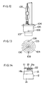
- the discharge lamp LA comprises an HID (high intensity discharge) lamp of such well known structure comprising, as shown in FIGS. 12 and 13 , a light emitting tube 103, a lamp base 105 having a flange 104, a center electrode 106, an outer peripheral electrode 107 and a pair of engaging projections 108 projected out of the periphery of the lamp base 105.
- HID high intensity discharge
- a socket body 2 is formed by integrally molding with a synthetic resin a case 14 for mounting therein the starting circuit section 10 as well as the socket and connector sections 11 and 12.
- the case 14 has a main circuit housing part 14a of a rectangular box shape opened on one surface and a transformer housing part 14b substantially of a cylindrical shape provided to project outward from the other surface opposite to the opened surface.
- main circuit housing part 14a other electronic parts 10b than the pulse transformer PT as well as the main circuit 10a comprising a plurality of the lead frames 13 are housed, while in the transformer housing part 14b the pulse transformer PT in which the primary and secondary windings 15a and 15b are wound on a ring-shaped core 15 are wound is housed.
- the connector section 12 is provided substantially in a rectangular cylinder projecting outward from one side face of the main circuit housing part 14a of the case 14.
- three input terminals 16a, 16b and 16c respectively connected to end portions of different lead frames 131-133 are fixed to the side face of the case 14 so as to conform their longitudinal direction to axial direction of the connector section 12 and to project inside the connector section 12.
- the socket section 11 is of a cylindrical, bottomed tubular shape, having at one end a lamp mounting opening 11a and projecting outward from a bottom face of the transformer housing part 14b of the case 14.
- the socket section 11 has, as main electrodes, a center electrode 17 contacting with the center electrode 106 of the lamp base 105 of the discharge lamp LA and an outer peripheral electrode 18 contacting with the outer peripheral electrode 107 of the lamp base 105 of the discharge lamp LA, and is further provided with an auxiliary electrode 19 of the same construction as the outer peripheral electrode 18 at a position opposing the outer peripheral electrode 18 with the center electrode 17 interposed between them.
- auxiliary electrode 19 and outer peripheral electrode 18 are so provided as to be mutually connected by means of the outer peripheral electrode 107 of the lamp base 105, when the lamp base 105 of the discharge lamp LA is inserted.
- inserting grooves 20 for inserting the engaging projections 108 projected from the periphery of the lamp base 105 and engaging grooves 21 communicating with the inserting grooves 20.
- angle projections 21a are provided at a side end face of the lamp mounting opening 11a at positions where the engaging grooves 21 communicates with the inserting grooves.
- the engaging projections 108 are brought, over the projections 21a, into engagement in the engaging grooves 21 communicating with the inserting grooves 20, upon which the center electrode 106 of the discharge lamp LA comes into conductive contact with the center electrode 17 of the lamp socket A, and the outer peripheral electrode 107 of the discharge lamp LA is contacted conductively, so as to be able to supply power to the discharge lamp LA.
- a slit 22 is provided in the peripheral part of the socket section 11 to be in parallel with the engaging groove 21, so as to render edge surface of the engaging grooves 21 opposing the slit 22 to be easily bendable, so that the arrangement may be made to allow the feeling of click to be attained upon passing of the engaging projection 108 over the projection 21a, whereby it is enabled to prevent the discharge lamp LA from being mounted in incomplete state with respect to the socket section 11.
- the lead frames 13 are formed in a strap shape, and are provided respectively at important points with recessed grooves 13a for mounting and connecting terminals (leads) of the electronic parts 10b or inserting holes 13b for inserting and connecting terminals of the windings of the pulse transformer PT.
- a lead frame 134connected to the center electrode 17 is disposed, and, around it, lead frames 135and 136connected respectively at their one end to the outer peripheral electrode 18 and auxiliary electrode 19 are disposed.
- the pulse transformer PT is housed within the transformer housing part 14b of the case 14, the plurality of lead frames 131... are housed from above and disposed in the case 14, the lead frames 131... are connected to the primary and secondary windings 15a and 15b, thereafter the electronic parts 10b are housed within the case 14 so as to dispose the terminals 10c in the recessed grooves 13a of the lead frames 131..., and the lead frames 131... and terminals 10c are connected through such proper means as the laser welding, spot welding, resistance welding, soldering or the like, whereby the starting circuit section 10 can be formed. Further, the interior of the socket body 2 is filled with a resin, the opening of the case is closed with a flat-plate shaped lid 23, and the lamp socket A is completed.
- the starting circuit has been constituted conventionally by mounting the electronic parts to the printed circuit substrate, therefore, the electronic parts 10a of the starting circuit section 10 are electrically connected by the lead frames 131... in the present invention, so that the printed circuit substrate is not required to be used, the case 14 for housing the starting circuit section 10 and eventually the socket body 2 can be reduced in the volume, and the dimensional minimization is made possible.
- the lead frames 131..., input terminals 16a-16c and output terminals are constituted as separate parts, it is also possible to constitute them integrally by means of a press molding, to simultaneously mold them with the socket body 2 (insert molding), or to press-fit the lead frames 131 ... to the socket body 2.
- the socket body 2 is constituted by forming integrally the socket section 11, connector section 12 and case 14 with the synthetic resin
- the fitting only of the fitting parts of the socket section 11 and connector section 12 to the fitting holes 24a and 24b of the case 14 involves a risk that the high voltage generated at the starting circuit section 10 leaks through a gap at the fitting parts to deteriorate the insulation properties, but the fitting parts can be fixed without any gap by welding the fitting parts as in the above by means of the vibration welding or ultrasonic welding, and the insulation properties with respect to the high voltage yielded at the starting circuit section 10 can be also secured. Further, it is possible to prevent from occurring such inexpedience that the fitting parts are damaged due to vibration during running when the device is loaded on the automobile.
- a conductive member 25 which covers substantially the entirety of the socket body 2 is provided through a forming of a conductive resin, as shown in FIG. 16 , the socket body is shielded by this conductive member 25 so that any noise radiated from the starting circuit section 10 and discharge lamp LA accompanying the high voltage can be reduced.
- the terminals 10c of the electronic parts 10b and lead frames 131... are connected after housing the electronic parts in the case 14 and the opaque synthetic resin is filled in the case 14 to seal it
- the connecting work of the terminals 10c of the electronic parts 10b to the lead frames 131... is rendered easier, the presence of the electronic parts 10b can be confirmed even after their sealing with the resin 26, and absence or any abnormality of the electronic parts 10b can be easily confirmed.
- the terminals 10c of the electronic parts 10b generally have a plated layer formed on the surface of a copper made base, and such terminals 10c render the laser welding difficult.
- the lead frames 131... are provided with through holes 13c for passing therethrough the terminals 10c of the electronic parts 10b, and the terminals 10c of the electronic parts 10b are connected at peripheral edge of the through holes 13c, whereby the laser welding is made possible only with respect to the plated layer on the surface of the terminals 10c even when the terminals 10c of the electronic parts 10b are copper-made, so that the connecting work between the lead frames 131... and the electronic parts 10b can be made easier.
- the socket body 2 of the lamp socket A comprises a resin molded article formed from a synthetic resin having insulating properties and has the case 14 substantially of a box shape opened on one surface for housing the starting circuit section 10, and the transformer housing part 14b of a bottomed cylindrical shape is provided in the bottom part of the case 14.
- the case 14 is provided, on one side face, with the cylindrical connector section 12 and, on the bottom face of the transformer housing part 14b, with the socket section 11 having fitting recesses 11b for inserting fittings 53 of the discharge lamp LA.
- input terminals t11-t13 are respectively disposed to face an opening of the connector section 12 and, in the socket section 11, electrodes t21-t23 are respectively disposed in a state where their portions contacting with electrodes 55 and 56 of the discharge lamp LA are fitted in the fitting recesses 11b.
- a plurality of slits 11a opened on the side of open end of the socket section 11 are formed so that, when engaging pins 52 of the discharge lamp LA are placed at the positions of the slits 11a with the fittings 53 of the discharge lamp LA inserted in the fitting recesses 11b of the socket section 11 and the discharge lamp LA is rotated, the engaging pins 52 are engaged in the slits 11a, and the discharge lamp LA is held in the socket section 11.
- the arrangement is so made, at this point, that a central electrode 55 of the discharge lamp LA is electrically connected to the central electrode t21 of the socket section 11, and an outer peripheral electrode 56 of the discharge lamp LA is electrically connected to the outer peripheral electrode t22 and auxiliary electrode t23 of the socket section 11.
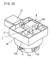
- a holding member 7 disposed between such electronic parts 10b as igniter main circuit 32 and noise filter F for holding the respective electronic parts 10b is mounted dismountably.
- the holding member 7 is substantially lattice-shaped, and the electronic parts 10b are respectively disposed in each of zones partitioned in lattice shape.
- Projections 8 are provided on wall surface of the holding member 7 or on inner walls of the case 14 so that, when the electronic parts 10b are incorporated in the case 14, the projections 8 engage with surfaces of the electronic parts 10b so as to hold the electronic parts 10b so that, even upon application of vibration or shock to the socket section 11, any mechanical stress can be prevented from being applied to connecting portions between the electronic parts 10b and later described lead frames 13, and the reliability in respect of the electric connection is improved.
- the holding member 7 is formed with the synthetic resin of insulating properties, it is possible to insulate between the respective electronic parts 10b by enclosing the respective electronic parts 10b with the holding member 7.
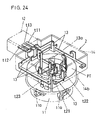
- the pulse transformer PT is housed, and in the case 14 the electronic parts 10b of the igniter main circuit 32 are accommodated.
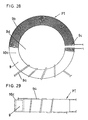
- the pulse transformer PT comprises, as shown in FIGS. 28 and 29 , a core 9 formed substantially in C-shape with part of an annular magnetic material cut off, and is formed by covering the surface of the core 9 with an insulating tape 10c and winding over the insulating tape 10c the primary winding 9a by 5 turns, for example, and further thereover the secondary winding 9b by 160 turns, for example.
- this pulse transformer PT comprises the core 9 insulated on the surface and the primary and secondary windings 9a and 9b wound on the core but is not provided with any coil bobbin, the pulse transformer PT can be dimensionally minimized by the volume of coil bobbin, and the dimensional minimization of the lamp socket A in the entirety can be attempted. By the way, both ends of the secondary winding 9b are led out of both sides of a cut-off part 9c of the core 9.
- the pulse transformer PT is housed within the transformer housing section 14b such that a projecting end part of the central electrode t21 in the case 14 is passed through a bore 9d of the core 9.
- the socket body 2 is provided with a projecting columnar insulating wall 30a covering around a position of the central electrode t21 which will project inside the case 14, and the insulating wall 30a covers around the central electrode t21, so that the insulation distance between the central electrode t21 and the electronic parts 10b of the igniter circuit 31 or of the noise filter F can be assured, and the socket body 2 is caused not to be dimensionally enlarged due to that the insulating distance is to be assured.
- the socket body 2 is provided with a projecting rib 30b which is to be inserted in the cut-off part 9c of the core 9 so that, as the pulse transformer PT is incorporated into the transformer housing part 14, the rib 30b enters in the cut-off part 9c, and both ends of the secondary winding 9b (that is, a starting side end and a terminating side end of the secondary winding 9b) are mutually insulated by the rib 30b While the high voltage is generated on the secondary side of the pulse transformer PT upon starting the discharge lamp LA, as has been described above, both ends of the secondary winding 9b are insulated by the rib 30b, and the socket body 2 is not dimensionally enlarged due to that the insulating distance between both ends of the secondary winding 9b is to be assured.
- the electronic parts 10b of the igniter circuit 31 and filter circuit F as well as a plurality of the lead frames 13 to be electrically connected to the input terminals t11-t13 or the respective lead frames 13 are accommodated.
- the lead frames 13 are to constitute electric paths of the interior circuits, and the interior circuits are formed, as shown in FIGS. 24 and 25 , by connecting through, for example, the welding the electronic parts 10b of the igniter circuit 31 and noise filter F and the input terminals t11-t13 or the respective electrodes t21-t23.
- the lead frames 13 and the input terminals t11-t13 or the respective electrodes t21-t23 are formed separately and connected, it is also possible to form integrally the lead frames 14 and input terminals t11-t13 and respective electrodes t21-23 by means of a press working of a conducting plate metal. Further, the lead frames 13, input terminals t11-t13 and respective electrodes t21-t23 may be simultaneously molded with the socket body 2, and the respective electronic parts 10b and lead frames 13 may be connected after the simultaneous molding by means of the force inserting or fitting of the respective electronic parts 10b into the socket body 2.
Landscapes
- Non-Portable Lighting Devices Or Systems Thereof (AREA)
- Connector Housings Or Holding Contact Members (AREA)
- Details Of Connecting Devices For Male And Female Coupling (AREA)
- Circuit Arrangements For Discharge Lamps (AREA)
Claims (3)
- Eine Lampenfassung, die folgende Merkmale aufweist:einen Fassungsabschnitt (11), an dem eine Entladungslampe demontierbar befestigt ist,einen Verbinderabschnitt (12) für eine elektrische Verbindung nach außen,einen Startschaltungsabschnitt (10), der eine Mehrzahl von elektronischen Teilen (10b) und Leitungsrahmen (13) umfasst, die zumindest mit einem Teil der elektronischen Teile verbunden sind, um Verdrahtungswege zwischen den jeweiligen elektronischen Teilen zum Anlegen einer hohen Spannung an die Entladungslampe zu bilden, um die Lampe zu starten, undein Gehäuse (14), in dem der Startschaltungsabschnitt vorgesehen ist,wobei der Fassungs- und der Verbinderabschnitt integriert mit dem Gehäuse vorgesehen sind, wobei die Startschaltung einen Pulstransformator (PT) aufweist, der einen Hochspannungspuls erzeugt, wobei der Pulstransformator durch einen Kern (9) gebildet ist, an dem Primär- und Sekundärwicklungen gewickelt sind,
dadurch gekennzeichnet, dass
der Kern ausgebildet ist, um einen weggeschnittenen Teil aufzuweisen, um C-förmig zu sein, und
das Gehäuse mit einer isolierenden Wand (30b) versehen ist, die in den weggeschnittenen Teil (9c) des Kerns eingesetzt ist. - Die Lampenfassung gemäß Anspruch 1, bei der der Fassungsabschnitt in einer zylindrischen Form ausgebildet ist, die zu einer Lampenbasis (105) der Entladungslampe passt, wobei ein Umfangsteil des Abschnitts mit Einsatzrillen (200) zum Einsetzen von Ineingriffnahmevorsprüngen (108) in dieselben, die von einem Umfangsteil der Lampenbasis vorstehen, Ineingriffnahmerillen (21), die mit den Einsatzrillen in Verbindung stehen, zum Ermöglichen, dass die Ineingriffnahmevorsprünge in dieselben greifen, wenn die Entladungslampe gedreht wird, und Schlitzen (22) versehen ist, die parallel zu den Ineingriffnahmerillen verlaufen.
- Eine Entladungslampenbeleuchtungsvorrichtung, die die Lampenfassung gemäß Anspruch 1 oder 2 aufweist, wobei
die Lampenfassung (A) einen Beleuchtungsschaltungsabschnitt (1) zum Liefern einer Leistung an eine Entladungslampe umfasst, wobei eine Quellenleistung von einer Leistungsquelle empfangen wird,
der Verbinderabschnitt für eine Verbindung zwischen dem Beleuchtungsschaltungsabschnitt und dem Startschaltungsabschnitt konfiguriert ist,
mit dem Verbinderabschnitt eine Eingangsleitung von einer Beleuchtungssteuerschaltung zum Steuern eines Beleuchtungszustands der Entladungslampe verbunden ist,
das Gehäuse mit einem Haltebauglied (7) versehen ist, das zwischen der Mehrzahl der elektronischen Teile zum Halten der elektronischen Teile angeordnet ist,
die Startschaltung eine Einrichtung zum Erzeugen des Hochspannungspulses umfasst,
das Haltebauglied ausgebildet ist, um die elektronischen Teile einzuschließen, an die der Hochspannungspuls angelegt wird,
das Haltebauglied mit zumindest einem des Gehäuses, des Verbinderabschnitts und des Fassungskörpers integriert gebildet ist, und
das Haltebauglied mit einer Partition zum Partitionieren des Gehäuses in einen Raum, der die Hochspannungspulserzeugungseinrichtung häust, und einen Raum, der andere elektronische Teile als die Hochspannungserzeugungseinrichtung häust, versehen ist.
Applications Claiming Priority (5)
| Application Number | Priority Date | Filing Date | Title |
|---|---|---|---|
| JP28015699 | 1999-09-30 | ||
| JP28015499A JP3090448B1 (ja) | 1999-09-30 | 1999-09-30 | ランプソケット及び放電灯点灯装置 |
| JP28015499 | 1999-09-30 | ||
| JP28015699A JP3121595B1 (ja) | 1999-09-30 | 1999-09-30 | ソケット及び放電灯点灯装置 |
| PCT/JP2000/006844 WO2001024323A1 (fr) | 1999-09-30 | 2000-10-02 | Douille de lampe et dispositif de commande de lampe a decharge |
Publications (3)
| Publication Number | Publication Date |
|---|---|
| EP1189314A1 EP1189314A1 (de) | 2002-03-20 |
| EP1189314A4 EP1189314A4 (de) | 2002-10-30 |
| EP1189314B1 true EP1189314B1 (de) | 2009-09-09 |
Family
ID=26553649
Family Applications (1)
| Application Number | Title | Priority Date | Filing Date |
|---|---|---|---|
| EP00963045A Expired - Lifetime EP1189314B1 (de) | 1999-09-30 | 2000-10-02 | Lampenfassung und betätigungsanordnung einer entladungslampe |
Country Status (5)
| Country | Link |
|---|---|
| US (1) | US6429591B1 (de) |
| EP (1) | EP1189314B1 (de) |
| CN (1) | CN1146089C (de) |
| DE (1) | DE60042926D1 (de) |
| WO (1) | WO2001024323A1 (de) |
Families Citing this family (24)
| Publication number | Priority date | Publication date | Assignee | Title |
|---|---|---|---|---|
| ITRM20020594A1 (it) * | 2002-11-25 | 2004-05-26 | Sisti Lighting S P A De | Dispositivo perfezionato per l'accensione e l'alimentazione |
| ES2343621T3 (es) * | 2003-02-13 | 2010-08-05 | Rafael Sanchez Jimenez | Encendedor con placa de circuito impreso que incorpora las interconexiones del dispositivo complementario. |
| JP4302457B2 (ja) * | 2003-07-25 | 2009-07-29 | 三菱電機株式会社 | 放電灯点灯装置 |
| DE10339591A1 (de) * | 2003-08-26 | 2005-03-24 | Patent-Treuhand-Gesellschaft für elektrische Glühlampen mbH | Lampensockel für eine Hockdruckentladungslampe und Hochdruckentladungslampe |
| DE10339594A1 (de) | 2003-08-26 | 2005-03-24 | Patent-Treuhand-Gesellschaft für elektrische Glühlampen mbH | Lampensockel für eine Hochdruckentladungslampe und Hochdruckentladungslampe |
| DE10339588A1 (de) | 2003-08-26 | 2005-03-24 | Patent-Treuhand-Gesellschaft für elektrische Glühlampen mbH | Lampensockel für eine Hochdruckentladungslampe und Hochdruckentladungslampe |
| DE10339587A1 (de) * | 2003-08-26 | 2005-03-24 | Patent-Treuhand-Gesellschaft für elektrische Glühlampen mbH | Transformator, Lampensockel mit einem Transformator und Hochdruckentladungslampe |
| JP2005322515A (ja) * | 2004-05-10 | 2005-11-17 | Harison Toshiba Lighting Corp | 放電灯点灯装置 |
| KR100715387B1 (ko) * | 2004-05-10 | 2007-05-08 | 하리손 도시바 라이팅구 가부시키가이샤 | 방전등 점등 장치 |
| US20060291216A1 (en) * | 2005-06-14 | 2006-12-28 | Blumel Daniel M | Apparatus for reducing in size an igniter circuit and assembly |
| DE102005038043A1 (de) * | 2005-08-09 | 2007-02-15 | Patent-Treuhand-Gesellschaft für elektrische Glühlampen mbH | Lampensockel für eine Hochdruckentladungslampe und Hochdruckentladungslampe |
| DE102005041719B4 (de) * | 2005-09-01 | 2016-09-29 | Osram Gmbh | Elektrische Lampe mit einem im Sockelinnenteil eingespritzten U-förmigen Haltering |
| US7772780B2 (en) * | 2006-12-27 | 2010-08-10 | General Electric Company | Lamp igniter module and transformer carrier |
| US20080225504A1 (en) * | 2007-03-14 | 2008-09-18 | Chichernea Virgil A | Lightweight electromagnetic interference shielding for automotive igniters |
| JP4541387B2 (ja) * | 2007-08-13 | 2010-09-08 | 株式会社小糸製作所 | 放電ランプ用ソケット |
| JP5135038B2 (ja) * | 2008-04-14 | 2013-01-30 | 株式会社小糸製作所 | 点灯装置 |
| DE102008048700A1 (de) * | 2008-09-24 | 2010-03-25 | Hella Kgaa Hueck & Co. | Scheinwerfer für Fahrzeuge |
| DE102008059561A1 (de) * | 2008-11-28 | 2010-06-10 | Osram Gesellschaft mit beschränkter Haftung | Integrierte Gasentladungslampe |
| WO2010060837A1 (de) * | 2008-11-28 | 2010-06-03 | Osram Gesellschaft mit beschränkter Haftung | Integrierte gasentladungslampe und zündtransformator für eine integrierte gasentladungslampe |
| JP2011077003A (ja) * | 2009-10-02 | 2011-04-14 | Koito Mfg Co Ltd | 車両用放電灯 |
| US20130100685A1 (en) * | 2010-07-14 | 2013-04-25 | Koninklijke Philips Electronics N.V. | Led lighting assembly with mounting element for optics |
| US20120162999A1 (en) * | 2010-12-22 | 2012-06-28 | Koninklijke Philips Electronics N.V. | Recessed luminaire with trim retaining mechanism and method thereof |
| US9239135B2 (en) | 2012-07-25 | 2016-01-19 | Tyco Electronics Corporation | LED connector |
| JP2015201260A (ja) * | 2014-04-04 | 2015-11-12 | 矢崎総業株式会社 | コネクタ装置 |
Family Cites Families (10)
| Publication number | Priority date | Publication date | Assignee | Title |
|---|---|---|---|---|
| US4258287A (en) * | 1979-06-13 | 1981-03-24 | General Electric Company | Circular fluorescent lamp unit |
| JPH08130127A (ja) | 1994-06-15 | 1996-05-21 | Nippondenso Co Ltd | 高圧トランス及び放電灯回路 |
| JPH08138872A (ja) | 1994-11-10 | 1996-05-31 | Nippondenso Co Ltd | 放電灯装置 |
| US6049659A (en) | 1995-12-26 | 2000-04-11 | Matsushita Electric Industrial Co., Ltd. | Method for automatically designing a semiconductor integrated circuit |
| DE69712859T2 (de) | 1996-12-07 | 2002-09-05 | Ngk Spark Plug Co., Ltd. | Steuerungsgerät für eine Fahrzeugbeleuchtung |
| JPH10223005A (ja) | 1996-12-07 | 1998-08-21 | Ngk Spark Plug Co Ltd | 車両用点灯起動装置 |
| JP3632183B2 (ja) * | 1997-01-28 | 2005-03-23 | 東洋電装株式会社 | 放電灯ユニット |
| JPH10255507A (ja) | 1997-03-06 | 1998-09-25 | Ngk Spark Plug Co Ltd | 車両用点灯起動装置 |
| US6084354A (en) * | 1997-03-06 | 2000-07-04 | Ngk Spark Plug Co., Ltd. | Vehicle-lamp lighting-on device |
| JP3752803B2 (ja) * | 1997-09-09 | 2006-03-08 | 東洋電装株式会社 | 放電灯点灯装置 |
-
2000
- 2000-10-02 WO PCT/JP2000/006844 patent/WO2001024323A1/ja active Application Filing
- 2000-10-02 CN CNB008017727A patent/CN1146089C/zh not_active Expired - Fee Related
- 2000-10-02 US US09/830,402 patent/US6429591B1/en not_active Expired - Lifetime
- 2000-10-02 EP EP00963045A patent/EP1189314B1/de not_active Expired - Lifetime
- 2000-10-02 DE DE60042926T patent/DE60042926D1/de not_active Expired - Lifetime
Also Published As
| Publication number | Publication date |
|---|---|
| WO2001024323A1 (fr) | 2001-04-05 |
| EP1189314A4 (de) | 2002-10-30 |
| US6429591B1 (en) | 2002-08-06 |
| CN1321349A (zh) | 2001-11-07 |
| CN1146089C (zh) | 2004-04-14 |
| EP1189314A1 (de) | 2002-03-20 |
| DE60042926D1 (de) | 2009-10-22 |
Similar Documents
| Publication | Publication Date | Title |
|---|---|---|
| EP1189314B1 (de) | Lampenfassung und betätigungsanordnung einer entladungslampe | |
| JP3632183B2 (ja) | 放電灯ユニット | |
| JP4426995B2 (ja) | 高電圧パルス発生器、及びそれを用いた照明器具、並びに車両 | |
| EP0886286B1 (de) | Hochspannungstransformator und Beleuchtungsvorrichtung mit Fahrzeuglampe dafür | |
| EP2025993B1 (de) | Entladelampensockel | |
| EP0852455B1 (de) | Steuerungsgerät für eine Fahrzeugbeleuchtung | |
| JPH08138872A (ja) | 放電灯装置 | |
| EP1744601B1 (de) | Anordnung zum Zünden einer Entladungslampe und Herstellungsverfahren dafür | |
| KR100570483B1 (ko) | 고압 방전 램프 점등 장치, 고압 방전 램프 장치 및 투광램프 장치 | |
| KR100402387B1 (ko) | 방전등 점등장치 | |
| JP2005072010A (ja) | 高圧放電ランプ用のランプ口金および高圧放電ランプ | |
| JP3090448B1 (ja) | ランプソケット及び放電灯点灯装置 | |
| JP2002343654A (ja) | 高電圧パルス発生器及びその製造方法 | |
| JP3867488B2 (ja) | ランプソケット | |
| JP3121595B1 (ja) | ソケット及び放電灯点灯装置 | |
| CN102612624B (zh) | 高压放电灯 | |
| JP4226158B2 (ja) | 放電灯装置 | |
| JP2003158022A (ja) | 高電圧トランスおよび高圧放電ランプ装置 | |
| JP4239870B2 (ja) | 放電灯始動装置、放電灯点灯装置、車両用前照灯器具、車両 | |
| JP2002216534A (ja) | 放電灯点灯装置およびその製造方法 | |
| JP4281596B2 (ja) | ソケット、放電灯点灯装置、車両用前照灯器具並びに車両 | |
| JPH1074643A (ja) | 高圧放電灯点灯装置の高電圧発生コイル | |
| JP2008034129A (ja) | 放電灯点灯装置 | |
| JPH10255507A (ja) | 車両用点灯起動装置 | |
| JP3093475B2 (ja) | 高圧放電ランプ装置 |
Legal Events
| Date | Code | Title | Description |
|---|---|---|---|
| PUAI | Public reference made under article 153(3) epc to a published international application that has entered the european phase |
Free format text: ORIGINAL CODE: 0009012 |
|
| 17P | Request for examination filed |
Effective date: 20010427 |
|
| AK | Designated contracting states |
Kind code of ref document: A1 Designated state(s): AT BE CH CY DE DK ES FI FR GB GR IE IT LI LU MC NL PT SE |
|
| A4 | Supplementary search report drawn up and despatched |
Effective date: 20020912 |
|
| AK | Designated contracting states |
Kind code of ref document: A4 Designated state(s): AT BE CH CY DE DK ES FI FR GB GR IE IT LI LU MC NL PT SE |
|
| RIC1 | Information provided on ipc code assigned before grant |
Free format text: 7H 01R 33/02 A, 7H 01R 33/945 B |
|
| RBV | Designated contracting states (corrected) |
Designated state(s): DE |
|
| 17Q | First examination report despatched |
Effective date: 20080219 |
|
| RAP1 | Party data changed (applicant data changed or rights of an application transferred) |
Owner name: PANASONIC ELECTRIC WORKS CO., LTD. |
|
| GRAP | Despatch of communication of intention to grant a patent |
Free format text: ORIGINAL CODE: EPIDOSNIGR1 |
|
| RIN1 | Information on inventor provided before grant (corrected) |
Inventor name: MIYAI, TAKAO Inventor name: KINUTANI, KAZUHIKO Inventor name: TAKAMATSU, KENICHI Inventor name: CHUZAWA, TAKAAKI |
|
| GRAS | Grant fee paid |
Free format text: ORIGINAL CODE: EPIDOSNIGR3 |
|
| GRAA | (expected) grant |
Free format text: ORIGINAL CODE: 0009210 |
|
| AK | Designated contracting states |
Kind code of ref document: B1 Designated state(s): DE |
|
| REF | Corresponds to: |
Ref document number: 60042926 Country of ref document: DE Date of ref document: 20091022 Kind code of ref document: P |
|
| PLBE | No opposition filed within time limit |
Free format text: ORIGINAL CODE: 0009261 |
|
| STAA | Information on the status of an ep patent application or granted ep patent |
Free format text: STATUS: NO OPPOSITION FILED WITHIN TIME LIMIT |
|
| 26N | No opposition filed |
Effective date: 20100610 |
|
| PGFP | Annual fee paid to national office [announced via postgrant information from national office to epo] |
Ref country code: DE Payment date: 20160927 Year of fee payment: 17 |
|
| REG | Reference to a national code |
Ref country code: DE Ref legal event code: R119 Ref document number: 60042926 Country of ref document: DE |
|
| PG25 | Lapsed in a contracting state [announced via postgrant information from national office to epo] |
Ref country code: DE Free format text: LAPSE BECAUSE OF NON-PAYMENT OF DUE FEES Effective date: 20180501 |