EP1184911A1 - Dispositif d'affichage d'un appareil electronique equipe d'une pile solaire - Google Patents
Dispositif d'affichage d'un appareil electronique equipe d'une pile solaire Download PDFInfo
- Publication number
- EP1184911A1 EP1184911A1 EP00974872A EP00974872A EP1184911A1 EP 1184911 A1 EP1184911 A1 EP 1184911A1 EP 00974872 A EP00974872 A EP 00974872A EP 00974872 A EP00974872 A EP 00974872A EP 1184911 A1 EP1184911 A1 EP 1184911A1
- Authority
- EP
- European Patent Office
- Prior art keywords
- solar cell
- solar
- display board
- polarizing plate
- electronic apparatus
- Prior art date
- Legal status (The legal status is an assumption and is not a legal conclusion. Google has not performed a legal analysis and makes no representation as to the accuracy of the status listed.)
- Withdrawn
Links
- 239000000758 substrate Substances 0.000 claims description 171
- 229920005989 resin Polymers 0.000 claims description 114
- 239000011347 resin Substances 0.000 claims description 114
- 239000010409 thin film Substances 0.000 claims description 52
- 239000010408 film Substances 0.000 claims description 36
- 229910052751 metal Inorganic materials 0.000 claims description 30
- 239000002184 metal Substances 0.000 claims description 30
- 239000010410 layer Substances 0.000 claims description 29
- 238000000034 method Methods 0.000 claims description 24
- 239000011521 glass Substances 0.000 claims description 20
- 239000000853 adhesive Substances 0.000 claims description 17
- 230000001070 adhesive effect Effects 0.000 claims description 17
- 239000004744 fabric Substances 0.000 claims description 14
- 238000009792 diffusion process Methods 0.000 claims description 11
- 238000005323 electroforming Methods 0.000 claims description 11
- 238000012546 transfer Methods 0.000 claims description 11
- 239000012790 adhesive layer Substances 0.000 claims description 10
- 238000004040 coloring Methods 0.000 claims description 10
- 238000004519 manufacturing process Methods 0.000 claims description 10
- 239000000919 ceramic Substances 0.000 claims description 9
- 239000011888 foil Substances 0.000 claims description 8
- 229910052594 sapphire Inorganic materials 0.000 claims description 8
- 239000010980 sapphire Substances 0.000 claims description 8
- 239000005445 natural material Substances 0.000 claims description 7
- 239000002023 wood Substances 0.000 claims description 7
- 239000004973 liquid crystal related substance Substances 0.000 claims 1
- 238000013461 design Methods 0.000 abstract description 68
- 238000001746 injection moulding Methods 0.000 abstract description 31
- 210000004027 cell Anatomy 0.000 description 154
- 230000000694 effects Effects 0.000 description 29
- 239000000463 material Substances 0.000 description 15
- 238000005034 decoration Methods 0.000 description 13
- 238000010521 absorption reaction Methods 0.000 description 10
- 238000002834 transmittance Methods 0.000 description 9
- 239000003292 glue Substances 0.000 description 8
- 238000002844 melting Methods 0.000 description 7
- 230000008018 melting Effects 0.000 description 7
- 238000000465 moulding Methods 0.000 description 7
- 238000010248 power generation Methods 0.000 description 7
- 229910052611 pyroxene Inorganic materials 0.000 description 7
- PXHVJJICTQNCMI-UHFFFAOYSA-N Nickel Chemical compound [Ni] PXHVJJICTQNCMI-UHFFFAOYSA-N 0.000 description 6
- 230000003247 decreasing effect Effects 0.000 description 6
- 239000010985 leather Substances 0.000 description 6
- 230000005540 biological transmission Effects 0.000 description 5
- 238000007639 printing Methods 0.000 description 5
- 238000012545 processing Methods 0.000 description 5
- -1 that is Substances 0.000 description 5
- 238000003754 machining Methods 0.000 description 4
- 230000010355 oscillation Effects 0.000 description 4
- 238000007747 plating Methods 0.000 description 4
- VYPSYNLAJGMNEJ-UHFFFAOYSA-N Silicium dioxide Chemical compound O=[Si]=O VYPSYNLAJGMNEJ-UHFFFAOYSA-N 0.000 description 3
- 239000003086 colorant Substances 0.000 description 3
- 230000003111 delayed effect Effects 0.000 description 3
- 229910052759 nickel Inorganic materials 0.000 description 3
- 239000000049 pigment Substances 0.000 description 3
- 239000004417 polycarbonate Substances 0.000 description 3
- 229920000515 polycarbonate Polymers 0.000 description 3
- 238000003825 pressing Methods 0.000 description 3
- 238000005406 washing Methods 0.000 description 3
- KRHYYFGTRYWZRS-UHFFFAOYSA-N Fluorane Chemical compound F KRHYYFGTRYWZRS-UHFFFAOYSA-N 0.000 description 2
- XEEYBQQBJWHFJM-UHFFFAOYSA-N Iron Chemical compound [Fe] XEEYBQQBJWHFJM-UHFFFAOYSA-N 0.000 description 2
- BQCADISMDOOEFD-UHFFFAOYSA-N Silver Chemical compound [Ag] BQCADISMDOOEFD-UHFFFAOYSA-N 0.000 description 2
- 230000002411 adverse Effects 0.000 description 2
- 229910045601 alloy Inorganic materials 0.000 description 2
- 239000000956 alloy Substances 0.000 description 2
- 230000003796 beauty Effects 0.000 description 2
- 230000015572 biosynthetic process Effects 0.000 description 2
- 238000005530 etching Methods 0.000 description 2
- 238000002474 experimental method Methods 0.000 description 2
- 238000010438 heat treatment Methods 0.000 description 2
- 230000010354 integration Effects 0.000 description 2
- 239000003973 paint Substances 0.000 description 2
- KMUONIBRACKNSN-UHFFFAOYSA-N potassium dichromate Chemical compound [K+].[K+].[O-][Cr](=O)(=O)O[Cr]([O-])(=O)=O KMUONIBRACKNSN-UHFFFAOYSA-N 0.000 description 2
- 230000035939 shock Effects 0.000 description 2
- 229910052709 silver Inorganic materials 0.000 description 2
- 239000004332 silver Substances 0.000 description 2
- 238000011282 treatment Methods 0.000 description 2
- ZCYVEMRRCGMTRW-UHFFFAOYSA-N 7553-56-2 Chemical compound [I] ZCYVEMRRCGMTRW-UHFFFAOYSA-N 0.000 description 1
- 229910001369 Brass Inorganic materials 0.000 description 1
- 229910000906 Bronze Inorganic materials 0.000 description 1
- RYGMFSIKBFXOCR-UHFFFAOYSA-N Copper Chemical compound [Cu] RYGMFSIKBFXOCR-UHFFFAOYSA-N 0.000 description 1
- 229910000881 Cu alloy Inorganic materials 0.000 description 1
- OAICVXFJPJFONN-UHFFFAOYSA-N Phosphorus Chemical compound [P] OAICVXFJPJFONN-UHFFFAOYSA-N 0.000 description 1
- 239000004372 Polyvinyl alcohol Substances 0.000 description 1
- RTAQQCXQSZGOHL-UHFFFAOYSA-N Titanium Chemical compound [Ti] RTAQQCXQSZGOHL-UHFFFAOYSA-N 0.000 description 1
- 230000004308 accommodation Effects 0.000 description 1
- 239000002253 acid Substances 0.000 description 1
- KGBXLFKZBHKPEV-UHFFFAOYSA-N boric acid Chemical compound OB(O)O KGBXLFKZBHKPEV-UHFFFAOYSA-N 0.000 description 1
- 239000004327 boric acid Substances 0.000 description 1
- 239000010951 brass Substances 0.000 description 1
- 239000010974 bronze Substances 0.000 description 1
- 239000003990 capacitor Substances 0.000 description 1
- 239000001913 cellulose Substances 0.000 description 1
- 229920002678 cellulose Polymers 0.000 description 1
- 238000006243 chemical reaction Methods 0.000 description 1
- 239000011248 coating agent Substances 0.000 description 1
- 238000000576 coating method Methods 0.000 description 1
- 229910052681 coesite Inorganic materials 0.000 description 1
- 229910052802 copper Inorganic materials 0.000 description 1
- 239000010949 copper Substances 0.000 description 1
- KUNSUQLRTQLHQQ-UHFFFAOYSA-N copper tin Chemical compound [Cu].[Sn] KUNSUQLRTQLHQQ-UHFFFAOYSA-N 0.000 description 1
- 229910052906 cristobalite Inorganic materials 0.000 description 1
- 238000005520 cutting process Methods 0.000 description 1
- 238000005238 degreasing Methods 0.000 description 1
- 238000010586 diagram Methods 0.000 description 1
- 230000005611 electricity Effects 0.000 description 1
- 239000003822 epoxy resin Substances 0.000 description 1
- PCHJSUWPFVWCPO-UHFFFAOYSA-N gold Chemical compound [Au] PCHJSUWPFVWCPO-UHFFFAOYSA-N 0.000 description 1
- 229910052737 gold Inorganic materials 0.000 description 1
- 239000010931 gold Substances 0.000 description 1
- 238000010348 incorporation Methods 0.000 description 1
- 238000002347 injection Methods 0.000 description 1
- 239000007924 injection Substances 0.000 description 1
- 238000003780 insertion Methods 0.000 description 1
- 230000037431 insertion Effects 0.000 description 1
- 239000011630 iodine Substances 0.000 description 1
- 229910052740 iodine Inorganic materials 0.000 description 1
- 238000007733 ion plating Methods 0.000 description 1
- 229910052742 iron Inorganic materials 0.000 description 1
- 239000002649 leather substitute Substances 0.000 description 1
- 239000007788 liquid Substances 0.000 description 1
- 238000006386 neutralization reaction Methods 0.000 description 1
- MOFOBJHOKRNACT-UHFFFAOYSA-N nickel silver Chemical compound [Ni].[Ag] MOFOBJHOKRNACT-UHFFFAOYSA-N 0.000 description 1
- 239000010956 nickel silver Substances 0.000 description 1
- KERTUBUCQCSNJU-UHFFFAOYSA-L nickel(2+);disulfamate Chemical compound [Ni+2].NS([O-])(=O)=O.NS([O-])(=O)=O KERTUBUCQCSNJU-UHFFFAOYSA-L 0.000 description 1
- 230000003287 optical effect Effects 0.000 description 1
- 230000000149 penetrating effect Effects 0.000 description 1
- 229920002120 photoresistant polymer Polymers 0.000 description 1
- 239000004033 plastic Substances 0.000 description 1
- 229920003023 plastic Polymers 0.000 description 1
- 239000002985 plastic film Substances 0.000 description 1
- 229920006255 plastic film Polymers 0.000 description 1
- 229920000647 polyepoxide Polymers 0.000 description 1
- 229920002451 polyvinyl alcohol Polymers 0.000 description 1
- 239000004800 polyvinyl chloride Substances 0.000 description 1
- 229920000915 polyvinyl chloride Polymers 0.000 description 1
- 230000001681 protective effect Effects 0.000 description 1
- 238000004080 punching Methods 0.000 description 1
- 229940000207 selenious acid Drugs 0.000 description 1
- MCAHWIHFGHIESP-UHFFFAOYSA-N selenous acid Chemical compound O[Se](O)=O MCAHWIHFGHIESP-UHFFFAOYSA-N 0.000 description 1
- 239000000377 silicon dioxide Substances 0.000 description 1
- 238000004544 sputter deposition Methods 0.000 description 1
- 239000010935 stainless steel Substances 0.000 description 1
- 229910001220 stainless steel Inorganic materials 0.000 description 1
- 229910052682 stishovite Inorganic materials 0.000 description 1
- 239000000126 substance Substances 0.000 description 1
- 229920005992 thermoplastic resin Polymers 0.000 description 1
- 239000010936 titanium Substances 0.000 description 1
- 229910052719 titanium Inorganic materials 0.000 description 1
- 229910052905 tridymite Inorganic materials 0.000 description 1
- 238000007738 vacuum evaporation Methods 0.000 description 1
- 238000003466 welding Methods 0.000 description 1
Images


Classifications
-
- H—ELECTRICITY
- H01—ELECTRIC ELEMENTS
- H01L—SEMICONDUCTOR DEVICES NOT COVERED BY CLASS H10
- H01L31/00—Semiconductor devices sensitive to infrared radiation, light, electromagnetic radiation of shorter wavelength or corpuscular radiation and specially adapted either for the conversion of the energy of such radiation into electrical energy or for the control of electrical energy by such radiation; Processes or apparatus specially adapted for the manufacture or treatment thereof or of parts thereof; Details thereof
- H01L31/04—Semiconductor devices sensitive to infrared radiation, light, electromagnetic radiation of shorter wavelength or corpuscular radiation and specially adapted either for the conversion of the energy of such radiation into electrical energy or for the control of electrical energy by such radiation; Processes or apparatus specially adapted for the manufacture or treatment thereof or of parts thereof; Details thereof adapted as photovoltaic [PV] conversion devices
- H01L31/054—Optical elements directly associated or integrated with the PV cell, e.g. light-reflecting means or light-concentrating means
-
- H—ELECTRICITY
- H01—ELECTRIC ELEMENTS
- H01L—SEMICONDUCTOR DEVICES NOT COVERED BY CLASS H10
- H01L31/00—Semiconductor devices sensitive to infrared radiation, light, electromagnetic radiation of shorter wavelength or corpuscular radiation and specially adapted either for the conversion of the energy of such radiation into electrical energy or for the control of electrical energy by such radiation; Processes or apparatus specially adapted for the manufacture or treatment thereof or of parts thereof; Details thereof
- H01L31/02—Details
- H01L31/0216—Coatings
- H01L31/02161—Coatings for devices characterised by at least one potential jump barrier or surface barrier
- H01L31/02167—Coatings for devices characterised by at least one potential jump barrier or surface barrier for solar cells
-
- G—PHYSICS
- G04—HOROLOGY
- G04C—ELECTROMECHANICAL CLOCKS OR WATCHES
- G04C10/00—Arrangements of electric power supplies in time pieces
- G04C10/02—Arrangements of electric power supplies in time pieces the power supply being a radioactive or photovoltaic source
-
- H—ELECTRICITY
- H01—ELECTRIC ELEMENTS
- H01L—SEMICONDUCTOR DEVICES NOT COVERED BY CLASS H10
- H01L31/00—Semiconductor devices sensitive to infrared radiation, light, electromagnetic radiation of shorter wavelength or corpuscular radiation and specially adapted either for the conversion of the energy of such radiation into electrical energy or for the control of electrical energy by such radiation; Processes or apparatus specially adapted for the manufacture or treatment thereof or of parts thereof; Details thereof
- H01L31/02—Details
-
- H—ELECTRICITY
- H01—ELECTRIC ELEMENTS
- H01L—SEMICONDUCTOR DEVICES NOT COVERED BY CLASS H10
- H01L31/00—Semiconductor devices sensitive to infrared radiation, light, electromagnetic radiation of shorter wavelength or corpuscular radiation and specially adapted either for the conversion of the energy of such radiation into electrical energy or for the control of electrical energy by such radiation; Processes or apparatus specially adapted for the manufacture or treatment thereof or of parts thereof; Details thereof
- H01L31/04—Semiconductor devices sensitive to infrared radiation, light, electromagnetic radiation of shorter wavelength or corpuscular radiation and specially adapted either for the conversion of the energy of such radiation into electrical energy or for the control of electrical energy by such radiation; Processes or apparatus specially adapted for the manufacture or treatment thereof or of parts thereof; Details thereof adapted as photovoltaic [PV] conversion devices
- H01L31/042—PV modules or arrays of single PV cells
- H01L31/048—Encapsulation of modules
-
- Y—GENERAL TAGGING OF NEW TECHNOLOGICAL DEVELOPMENTS; GENERAL TAGGING OF CROSS-SECTIONAL TECHNOLOGIES SPANNING OVER SEVERAL SECTIONS OF THE IPC; TECHNICAL SUBJECTS COVERED BY FORMER USPC CROSS-REFERENCE ART COLLECTIONS [XRACs] AND DIGESTS
- Y02—TECHNOLOGIES OR APPLICATIONS FOR MITIGATION OR ADAPTATION AGAINST CLIMATE CHANGE
- Y02E—REDUCTION OF GREENHOUSE GAS [GHG] EMISSIONS, RELATED TO ENERGY GENERATION, TRANSMISSION OR DISTRIBUTION
- Y02E10/00—Energy generation through renewable energy sources
- Y02E10/50—Photovoltaic [PV] energy
- Y02E10/52—PV systems with concentrators
-
- Y—GENERAL TAGGING OF NEW TECHNOLOGICAL DEVELOPMENTS; GENERAL TAGGING OF CROSS-SECTIONAL TECHNOLOGIES SPANNING OVER SEVERAL SECTIONS OF THE IPC; TECHNICAL SUBJECTS COVERED BY FORMER USPC CROSS-REFERENCE ART COLLECTIONS [XRACs] AND DIGESTS
- Y10—TECHNICAL SUBJECTS COVERED BY FORMER USPC
- Y10S—TECHNICAL SUBJECTS COVERED BY FORMER USPC CROSS-REFERENCE ART COLLECTIONS [XRACs] AND DIGESTS
- Y10S136/00—Batteries: thermoelectric and photoelectric
- Y10S136/291—Applications
Definitions
- the present invention relates to a display device for an electronic apparatus comprising a solar cell, for example, an electronic apparatus such as a watch, an electronic calculator, a radio, a battery charger, and more particularly the watch.
- Fig. 26(a) is a front view showing the inside of a watch case seen from above and Fig. 26B is a schematic sectional view showing the inside of the watch case.
- the solar cell 305 is such a mechanism that an optical energy is converted into an electric energy which is charged into a battery or capacitor referred to as a secondary battery which is provided in a module 307 and can store electricity, and simultaneously, the module 307 is conducted so that a minute hand 301 and an hour hand 309 which are fixed to a central shaft 308 are moved.
- the solar display board 301 is positioned between the minute hand 310 and hour hand 309 and the solar cell 305.
- the module 307 indicates a driving portion in the watch.
- a middle frame 306 is positioned on the outside of the solar cell 305 and the module 307 so that the degree of freedom can be enhanced in respect of the design of the external shape of the watch.
- the solar cell 305 and the module 307 are fixed through the middle frame 306 to an outer case which is not shown.
- the minute hand 310 and the hour hand 309 are bonded to the central shaft 308 extended from the module 307 and are rotated through driving force applied from the module 307.
- the solar display board 301 is provided to cover the solar cell 305 and the middle frame 306.
- the middle frame 306 is provided with a hook mechanism in order to fix the module 307 to which the solar cell 305 is fastened, which is not shown.
- the solar cell 305 and the module 307 are fixed to the middle frame 306 and are accommodated in the outer case and thus fixed therein.
- the solar cell 305 has two kinds of substrates, that is, substrates formed of a glass and a resin. For both of them, the solar cell itself has a small thickness. Furthermore, there is a possibility that the substrate formed of a glass might be chipped through a stress such as a shock during or after assembly. The substrate formed of a resin might be deformed by a stress thereof during bonding. For a method of fixation to the watch case, therefore, the solar cell 305 and the middle frame 306 are not fixed but the module 307 and the middle frame 306 are fixed. In the case of the substrate formed of a resin, a metal plate may be provided on the lower face of the solar cell 305 in order to enhance the reliability of rigidity and electrical connection.
- the middle frame 306 also has the function of preventing the reduction of the power generation.
- the middle frame 306 is protruded slightly upward from the upper face of the solar cell 305 such that the middle frame 306 comes in contact with the solar display board 301 earlier than the solar cell 305.
- the middle frame in watch parts is a member for playing an important role.
- a boundary line 303 between the solar cell 305 and the middle frame 306 usually requires a clearance for a watch assembling work and the clearance is seen to be black through the solar display board 301.
- a plastic material is often used for the middle frame 306 in consideration of easiness of molding, a cost, a shock absorption and the like, and the middle frame 306 is fabricated through injection molding to correspond to various outer cases. Therefore, a gate track 304 is formed on an upper face of the middle frame 306 due to the injection molding and the gate track 304 is also seen through the solar display board 301.
- a refractive index of light is varied depending on a difference in a material between a cell portion and a dividing line portion and a solar cell element dividing line 302 is also seen through the solar display board 301.
- Fig. 26 shows an example in which the solar cell element dividing line 302 has a cross-shape and the boundary line 303 between the solar cell 305 and the middle frame 306 has the shape of a black ring on the boundary between a slant line portion and a dotted portion.
- the diffusing board has the function of diffusing light. Therefore, the boundary line 303 between the solar cell 305 and the middle frame, the gate track 304 generated through the injection molding of the middle frame, and furthermore, the solar cell element dividing line 302 are seen with difficulty. As a result, they are necessarily seen to be white so that the tone of the solar display board 301 provided thereabove is affected.
- a black solar display board is seen to be gray, which is not preferable in respect of design.
- a white solar display board has diffusion effects by itself. Therefore, even if the diffusing board is not used, there is not such a phenomenon that the boundary line 303 between the solar cell 305 and the middle frame 306, the gate track 304 generated through the injection molding of the middle frame 306, and furthermore, the solar cell element dividing line 302 are seen through the solar display board 301. Therefore, it is not necessary to provide the diffusing board as in the Japanese Patent Publication No. Hei 5-38464.
- the solar display board 301 Usually, various designs are given through the solar display board 301. If there is such a phenomenon that the boundary line 303, the gate track 304 and the solar cell element dividing line 302 are seen as described above, the quality of design of a watch is adversely affected. More specifically, in this case, a decoration or the like should be given to a part of the solar display board 301 or the whole surface thereof in order to hide the above-mentioned phenomenon. Therefore, the design for the solar display board 301 is restricted so that a feeling of high quality for a watch is eliminated.
- the solar cell element dividing line 302 can be considerably improved by giving a protective coat formed of an epoxy resin which has SiO 2 particulates distributed therein over the whole surface of the solar cell 305.
- the gate track 304 generated during the injection molding of the middle frame 306 can also be improved by changing a gate position.
- the boundary line 303 between the solar cell 305 and the middle frame 306, that is, the clearance cannot be avoided for the watch assembling work and is the most harmful and measures are taken with difficulty.
- the colors of black and blue solar display boards are caused to be deeper, a feeling of high quality can be obtained for goods by the deeper colors, and furthermore, it is possible to eliminate such a drawback that the observation through the solar display board described above is caused.
- transmitted light does not fully reach the solar cell itself so that the power generation efficiency is reduced and the operation of the watch is stopped.
- the tone of the middle frame is adapted to that of the solar cell, it is possible to eliminate such a drawback that the observation through the solar display board described above is caused.
- the boundary line between the solar cell and the middle frame is seen so that the drawback cannot be eliminated completely.
- a white paint is thinly applied to the solar cell side of the blue solar display board having a blue resin kneaded therein, it is possible to eliminate such a phenomenon that the boundary line 303 between the solar cell 305 and the middle frame 306, the gate track 304 generated through the injection molding of the middle frame 306, and furthermore, the solar cell element dividing line 302 are seen through the solar display board 301.
- the depth of the color of the solar display board 301 is eliminated by the diffusing function of the white paint so that the feeling of high quality for the single solar display board disappears. In other words, the formation of a diffusion layer cannot obtain sufficient effects.
- a display board such as a watch dial
- various coloring and patterns are applied to the surface or back of the display board or both of them in order to give a feeling of high quality (added value) in some cases.
- the coloring is carried out by printing the surface of a material to be the display board or manufacturing the display board from a resin containing a pigment, for example.
- the pattern on the surface thereof is formed through etching, a mat processing or the like.
- a pattern is formed by injection molding the resin in a mold having the pattern formed therein.
- a display device for an electronic apparatus comprising a solar cell and a middle frame for fixing the solar cell and a module to an outer case in which necessary and sufficient light can be caused to reach the solar cell, a feeling of high quality can be given, and furthermore, it is possible to increase a variation in design in which a decorative property is great and the depth of a pattern and a three-dimensional effect are excellent.
- the present invention has been made to solve the problems of the conventional art described above and to achieve the above-mentioned object and provides a display device for an electronic apparatus comprising a solar cell, wherein a circular polarizing plate for transmitting light is provided on the front side of the solar cell in a direction of incidence of light.
- a circular polarizing plate constituted by a linear polarizing plate and a phase difference plate
- the linear polarizing plate and the phase difference plate are provided in this order in a direction of incidence of light. Consequently, light reflected by a solar cell surface can be blocked, a boundary line between the solar cell and the middle frame, a gate track generated through injection molding of the middle frame, and a solar cell element dividing line cannot be seen through the circular polarizing plate.
- the tone of the solar display board is not affected. Moreover, it is not necessary to hide the three drawbacks through a stripe-shaped pattern or the like. Thus, a variation in design of the solar display board can be increased. Furthermore, a solar display board having a deep color can be used so that a feeling of high quality can visually be obtained as goods. By directly giving marking such as a numeral to the linear polarizing plate by means of printing or the like, the function of the solar display board can also be given to the linear polarizing plate itself.
- the present invention is characterized in that the surface of the circular polarizing plate is provided with a solar display board constituted by a resin substrate having a pattern, an inorganic substrate having a pattern or a decorating thin film member or a combination thereof.
- a display device for an electronic apparatus comprising a solar cell capable of maintaining the necessary and sufficient power generation efficiency of the solar cell, giving a feeling of high quality and increasing a variation in design.
- the circular polarizing plate is usually fabricated by bonding a linear polarizing plate 111 formed of a film material to a 1/4 ⁇ plate 112 formed of a film material with an adhesive layer.
- a linear polarizing plate may have such a structure that a polyvinyl alcohol thin film absorbing iodine is extended in one direction and molecules are arranged in parallel and are sandwiched with acetylbutyl cellulose.
- a lens or lens group for collecting light in one direction may be used. Since mirror reflection can be suppressed, the linear polarizing plate is used for improving a contrast or lessening the fatigue of eyes.
- the linear polarizing plate 111 has an absorption type or a reflection type.
- An absorption axis or a reflection axis is present orthogonally to a transmission axis.
- the absorption type the light incident on the linear polarizing plate, 111 is absorbed in the polarizing plate.
- the reflection type has the function of reflecting the light incident on the linear polarizing plate 111 from a surface of the polarizing plate.
- the transmitted light polarized in one direction is incident at an angle of 45° with respect to a delay axis of the phase difference plate.
- the phase difference plate represents the 1/4 ⁇ plate 112, and divides the light incident at 45° into x and y directions for convenience and regards both maximum amplitudes as 1 as shown in Fig. 28.
- An axis of abscissa indicates an angle and an axis of ordinate indicates an amplitude, and the relationship between a wavelength and a phase is such that one wavelength is 360° ( ⁇ ). If the delay axis of the phase difference plate is set to the y direction, the presence of the phase difference plate causes the light transmitted through the phase difference plate to be delayed by a 1/4 ⁇ phase in only the y direction.
- the light thus circularly polarized is reflected by the surfaces of a middle frame 113 and a solar cell 114, and is incident on the 1/4 ⁇ plate 112 again reversely to a direction of advance as shown in Fig. 27.
- the light is converted into light having an oscillation plane in a direction perpendicular to the direction of incidence on the 1/4 ⁇ plate 112 and the light thus obtained is vertical to the transmission axis of the linear polarizing plate 111. Therefore, the light cannot pass through the linear polarizing plate 111 so that reflected light is blocked.
- the linear polarizing plate 111 and the 1/4 ⁇ plate 112 are combined to constitute a circular polarizing plate.
- the incident light is reflected by approximately several % per boundary surface if the boundary surfaces having different refractive indices are generally present. In the case of air and a glass, the incident light is reflected by approximately 4 %. Therefore, it is preferable that the number of boundary surfaces should be decreased as greatly as possible. Accordingly, it is preferable that the linear polarizing plate 111 and the 1/4 ⁇ plate 112 should be stacked in a close contact state or should be bonded with an adhesive or a glue.
- linear polarizing plate 111, the 1/4 ⁇ plate 112 and the middle frame 113 are square-shaped and the solar cell 114 is circular in Fig. 27, various other shapes may be used corresponding to design.
- a watch having a solar cell comprises a solar cell 13 electrically connected to a module 14, and a minute hand 17 and an hour hand 16 which are fixed to a central shaft 15.
- a circular polarizing plate A including a linear polarizing plate 11 and a 1/4 ⁇ plate 12 is provided between the hands 16 and 17 and the solar cell 13.
- marking such as a numeral is directly given to the linear polarizing plate 11 by means of printing to provide a function as a solar display board.
- the circular polarizing plate A constituted by the linear polarizing plate 11 and the 1/4 ⁇ plate 12 should have a plane direction positioned by an outer case which is not shown in respect of a watch assembling work.
- the description of the minute and hour hands will be omitted if there is no special condition.
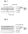
- a circular polarizing plate A including a linear polarizing plate 22 and a 1/4 ⁇ plate 23 is provided between a solar cell 24 and a solar display board 21 having a light transmittance.
- a module 25 is fabricated and the external shapes of the solar display board 21, the solar cell 24, the linear polarizing plate 22 and the 1/4 ⁇ plate 23 are simultaneously processed through press molding or the like and they are superposed with a structure shown in Fig. 2 in an outer case which is not shown so that a finished watch is obtained. Accordingly, it is desirable that the circular polarizing plate constituted by the solar display board 21, the solar cell 24, the linear polarizing plate 22 and the 1/4 ⁇ plate 23 should have the same external shapes.
- Fig. 3 shows a structure of a watch in which a module 34 having a solar cell 33 is fixed into an outer case 39 through a middle frame 35.
- a circular polarizing plate A constituted by a linear polarizing plate 31 and a 1/4 ⁇ plate 32 is provided above the middle frame 35 between a minute hand 37 and an hour hand 36 which are fixed to a central shaft 38 and the solar cell 33.
- the circular polarizing plate A should be provided to cover the solar cell 33 and the middle frame 35 as shown.
- the color of the surface of the linear polarizing plate 31 is deepened so that a feeling of high quality can be obtained as goods.
- marking such as a numeral is directly given to the linear polarizing plate 31 by means of printing to provide a function as a solar display board.
- the middle frame 35 is provided. Therefore, various external shapes of the watch can be obtained in respect of design. In the following embodiments, since effects are not affected, the description of the outer case will be omitted.
- Fig. 4 shows a structure of a watch in which a module 45 having a solar cell 44 is fixed through a middle frame 46 into an outer case which is not shown.
- a circular polarizing plate A constituted by a linear polarizing plate 42 and a 1/4 ⁇ plate 43 is provided between the middle frame 46 and a solar display board 41.
- a boundary line between the solar cell 44 and the middle frame 46, a gate track generated through injection molding of the middle frame 46, and furthermore, a solar cell element dividing line of the solar cell 44 cannot be seen through the solar display board 41 so that a variation in design of the solar display board 41 can be increased. Furthermore, the color of the solar display board 41 is deepened so that a feeling of high quality can be obtained as goods. Moreover, the middle frame 46 is provided. Therefore, various external shapes of the watch can be obtained in respect of design.
- a color display board including a dye, a pigment and the like is used for the solar display board 41, for example. Therefore, although a tone has only a black color in the third embodiment, the display board can have colors. Thus, it is apparent that practical use can be enhanced considerably in respect of the design.
- the circular polarizing plate A constituted by the linear polarizing plate 42 and the 1/4 ⁇ plate 43, the middle frame 46 and the solar display board 41 should have the same external shapes in respect of an assembling work.
- Fig. 5 shows a structure of a watch in which a module 56 having a solar cell 55 is fixed through a middle frame 57 into an outer case which is not shown.
- a circular polarizing plate B having a linear polarizing plate 52, a 1/4 ⁇ plate 53 and a 1/2 ⁇ plate 54 stacked is used.
- the circular polarizing plate B is provided between the middle frame 57 and a solar display board 51.
- the same effects as those in the fourth embodiment can be obtained. It has been known that the provision of the 1/2 ⁇ plate 54 can enlarge a wavelength region in which light can be blocked and a wideband type circular polarizing plate can be obtained.
- the 1/2 ⁇ plate includes a delay axis and has the function of delaying light incident in that direction by 1/2 ⁇ .
- a solar display board 61, a linear polarizing plate 62 and a 1/4 ⁇ plate 63 are bonded through an adhesive layer 68 and are then pressurized and molded.
- a circular polarizing.plate integral type solar display board C is fabricated.
- the circular polarizing plate integral type solar display board C is provided above a solar cell 64 having a diffusion layer 67 preformed on an upper surface thereof.
- a boundary line between the solar cell 64 and a middle frame 66, a gate track generated through injection molding of the middle frame 66, and furthermore, a solar cell element dividing line of the solar cell 64 cannot be seen through the solar display board 61.
- a variation in design of the solar display board 61 can be increased.
- the color of the solar display board 61 is deepened so that a feeling of high quality can be obtained as goods.
- the middle frame 66 is provided. Therefore, various external shapes of the watch can be obtained in respect of design.
- the number of boundary surfaces is decreased from 7 to 3.
- the light transmitted to the solar cell 64 can be more enhanced and a power generation efficiency can be more improved as compared with the case in which the adhesive layer 68 is not provided.
- the diffusion layer 67 is first formed on the surface of the solar cell 64, is bonded to a module 65 and is then fitted in the middle frame 66.
- the solar display board 61, the linear polarizing plate 62 and the 1/4 ⁇ plate 63 are bonded together through the adhesive layer 68, and the external shape and perforation processings are then carried out through a press or the like. As shown, subsequently, they are superposed on an outer case which is not shown. Thus, a finished watch is obtained.
- the solar display board 61, the linear polarizing plate 62 and the 1/4 ⁇ plate 63 are bonded through the adhesive layer 68, they can be treated as one member.
- the work for assembling a watch can be carried out most easily in the embodiments.
- a solar display board 71, a linear polarizing plate 72, a 1/4 ⁇ plate 73, a solar cell 74 and a middle frame 76 are stacked as shown and are bonded with an adhesive layer 77.
- the color of the solar display board 71 is deepened so that a feeling of high quality can be obtained as goods.
- the middle frame 76 is provided. Therefore, various external shapes of the watch can be obtained in respect of the design.
- the number of boundary surfaces provided between the solar display board 71 and the air is one and a transmittance can be more enhanced than that in the sixth embodiment and a power generation efficiency can also be improved.
- a solar cell 83 is larger than the external shape of a module 84 and the external shape of a middle frame 85 for fixing the module 84 to an outer case which is not shown is equal to that of the solar cell 83.
- the solar cell 83 wholly covers a boundary line between the middle frame 85 and the module 84 and a gate track generated through injection molding of the middle frame 85. Therefore, the quality of display is not reduced.
- a linear polarizing plate 81 and a 1/4 ⁇ plate By inserting a linear polarizing plate 81 and a 1/4 ⁇ plate, a solar cell element dividing line of the solar cell 83 can be prevented from being seen.
- the present embodiment provides a watch structure in which a solar cell 94 and a module 95 are fixed through a middle frame 96 to an outer case which is not shown.
- a circular polarizing plate A constituted by a linear polarizing plate 92 and a 1/4 ⁇ plate 93 is provided above the middle frame 96. Furthermore, an LCD panel 91 is provided thereabove.
- the LCD panel 91 having a smaller external shape than that of the solar cell 94 is provided above the circular polarizing plate A. Consequently, light transmitted through the linear polarizing plate 92 and the 1/4 ⁇ plate 93 reaches the solar cell 94, and power is supplied to the LCD panel to display a time by electromotive force of the solar cell 94.
- the LCD panel displays a time of 12 o'clock in the afternoon.
- a linear polarizing plate has an absorption type and a reflection type.
- a reflection type linear polarizing plate having a reflection axis orthogonal to a transmission axis is used.
- a reflection type linear polarizing plate 42' is used as a linear polarizing plate 42 as in another embodiment, for example, as shown in Fig. 10.
- a boundary line between a solar cell 44 and a middle frame 46, a gate track generated through injection molding of a middle frame 46, and furthermore, a solar cell element dividing line of a solar cell 44 cannot be seen through a solar display board 41.
- a variation in design of the solar display board 41 can be increased in the same manner as in the fourth embodiment.
- a brightness is decreased and the blue color of the solar display board is deepened by using the absorption type linear polarizing plate and the blue color of the solar display board is reproduced faithfully by using the reflection type linear polarizing plate.
- a black solar display board moreover, a brightness is also decreased and a feeling of high quality can be obtained by using the absorption type linear polarizing plate and a brightness of the black color of the solar display board is increased to approximate to a gray color by using the reflection type linear polarizing plate.
- the color of the solar display board is changed in a deeper direction by using the absorption type linear polarizing plate, and a feeling of high quality can be obtained visually irrespective of the color of the solar display board.
- the absorption type is different from the reflection type in that an oscillation in a direction perpendicular to the transmission axis of the linear polarizing plate is absorbed in the linear polarizing plate or is reflected from the surface of the linear polarizing plate. Therefore, they carry out the same actions for transmitted light and have the same functions as the circular polarizing plates.
- a diffusion layer 47 is formed between the solar display board 41 and the linear polarizing plate 42 in the structure of Fig. 4.
- the color of the solar display board 41 is deepened and a feeling of high quality can be obtained as goods.
- the middle frame is provided. Therefore, various external shapes of a watch can be obtained in respect of the design.
- a diffusion layer 48 is formed between the linear polarizing plate 42 and the 1/4 ⁇ plate 43 in the structure of Fig. 4.
- the color of the solar display board 41 is deepened and a feeling of high quality can be obtained as goods.
- the middle frame is provided. Therefore, various external shapes of a watch can be obtained in respect of the design.
- oxide particulates are dispersed into an adhesive layer between the linear polarizing plate 42 and the 1/4 ⁇ plate 43 so that the diffusion layer is formed.
- a solar cell 102 and a module 104 are fixed through a middle frame 106 to an outer case which is not shown.
- a circular polarizing plate A constituted by a linear polarizing plate 101 and a 1/4 ⁇ plate 103 is provided above the middle frame 106. Furthermore, a solar display board 108 is provided thereabove.
- the solar display board 108 is constituted by a resin substrate body 110 and a pattern portion 112 formed on an upper surface thereof.
- the resin substrate 110 should be formed of a thermoplastic resin, and furthermore, a resin selected from the group consisting of polyvinyl chloride, an acryl resin and polycarbonate. In the present invention, it is particularly preferable that the acryl resin, or the polycarbonate should be used.
- a thickness of the resin substrate 110 is preferably approximately 50 to 500 ⁇ m, and more preferably approximately 80 to 200 ⁇ m.
- the resin substrate 11 may be transparent or be colored and translucent.
- a pattern is given to the resin substrate 110 by an injection molding method for injection molding a resin in a mold having a pattern formed thereon (which will be hereinafter referred to as a "pattern mold”); a pattern transfer method for transferring a pattern onto a resin substrate through a thermal press using the pattern mold; or a machining method using engraving, rubbing or the like.
- the pattern transfer method is preferably employed.
- the pattern transfer method As a method of giving a pattern to the resin substrate 110, the pattern transfer method will be described below.
- the pattern transfer method comprises the steps of manufacturing an electric mold 120 having a pattern surface and of thermally pressing a pattern surface 122 molded in the electric mold 120 against the resin substrate 110.
- a surface pattern of an article 124 having a pattern is first molded through an electric molding method. More specifically, the article 124 having the pattern is subjected to electroforming. In the case in which the article 124 does not have a conductivity, a metal film 126 is formed on the surface of the article 124 to give a conductivity to the article 124.
- Examples of the article 124 having the pattern include a cloth, a paper, a rift, a grain, a pyroxene, a leaf, a petal, a shell, a leather, artificial substances having various fine patterns (an artificial leather, engraving, chasing) and the like. It is preferable that the cloth, the paper, the rift, the grain, the pyroxene, the leaf, the engraving and the chasing should be used.
- a pattern is formed on the surface of the article 124 (concavo-convex portions on the surface in Fig. 15(A)).
- the back face of the article 124 is omitted.
- the surface of the article 124 is first cleaned and a metal film 126 is then formed on the surface of the article 124.
- the metal film 126 is formed by vacuum evaporation, ion plating, sputtering, nonelectrolytic plating, silver mirror reaction or the like, for example. While the metal film 126 is formed of a metal such as silver or gold or their alloy and a thickness thereof is not particularly restricted, a thickness of approximately 1 to 30 ⁇ m, preferably approximately 1 to 10 ⁇ m is suitable.
- the article 124 has a conductivity as described above, it is not necessary to form the metal film 126.
- the surface of the metal film 126 is subjected to removal if necessary.
- the surface of the article 124 is directly subjected to the removal.
- the removal can be carried out through injection of selenious acid.
- the electric mold 120 can easily be removed.
- a metal is deposited on the surface of the article 124 or the surface of the metal film 126 through the electric molding (electroforming) to form the electric mold 120.
- a metal such as nickel, copper or iron or their alloy is preferably used.
- a thickness of the electric mold 120 is 100 to 300 ⁇ m, preferably 100 to 250 ⁇ m, and more preferably 100 to 200 ⁇ m. If the thickness of the electric mold 120 is set in such a range, the resin substrate 110 is not deformed and heat transfer can be carried out well during a thermal press.
- the conditions of the electric molding are not particularly restricted but are properly selected from conventional electric molding (plating) conditions. There will be briefly described the electric molding conditions for obtaining the electric mold 120 having a thickness of 200 ⁇ m by using a nickel metal. However, the conditions should not be restricted by such a condition.
- the surface of the article 124 having a pattern or the metal film 126 is subjected to treatments of electrolytic degreasing, washing, acid neutralization, washing, removal (potassium dichromate) and washing.
- the electroforming is carried out at 265 AH (IA/dm 2 ) at a liquid temperature of 50°C by using a nickel plating bath (450 g/liter of nickel sulfamate, 40 g/liter of boric acid). Consequently, the electric mold 120 having a thickness of 200 ⁇ m is obtained.
- the electric mold 120 is removed from the surface of the article 124 or the surface of the metal film 126. Consequently, the electric mold 120 having a molded pattern surface is obtained. The electric mold 120 thus obtained is cut out corresponding to the shape of a display board to be intended if necessary.
- the molded pattern is transferred onto the resin substrate 110.
- the molded pattern surface of the electric mold 120 is opposed to the resin substrate 110 and are thermally pressed between a pair of upper and lower thermal presses 130 and 132.
- a thermal press temperature is generally set in the vicinity of a melting temperature of a resin, specifically, approximately 90 to 180°C is suitable.
- a temperature on the electric mold side should be set to 120 to 140°C and a temperate of a resin substrate should be set to approximately 40 to 80°C in a thermal press machine.
- a thermal press pressure is suitably set to approximately 20 to 100 kg/cm 2 .
- a time required for the thermal press should be set to approximately 10 to 180 seconds.
- preheating Prior to the thermal press of the resin substrate 110. preheating is carried out so that the time required for the thermal press can be shortened and productivity can be enhanced. It is preferable that a preheating temperature should be set to approximately 40 to 80°C. If such a preheating treatment is carried out, the time required for the thermal press can be shortened to approximately 10 to 30 seconds.
- the electric mold 120 may be bonded to a thermal press head during the thermal press. Consequently, the resin substrate 110 and the electric mold 120 can easily be removed from each other after the thermal press so that the productivity can be enhanced.
- the thermal press By the thermal press, the molded pattern 122 of the electric mold 120 is transferred onto the resin substrate 110 and the electric mold 120 is removed. Consequently, the resin substrate 110 having a pattern can be obtained.
- the electric mold 120 should be fixed to the upper and lower thermal press heads.
- the thermal press is to be successively carried out over both surfaces, moreover, it is preferable that the thermal press should be performed over one of the surfaces, the resin substrate 110 should be then turned over and the thermal press should be performed over the other surface.
- the resin substrate 110 having a pattern is manufactured independently one by one in the method of manufacturing the resin substrate 110 having a pattern described above. However, it is also possible to obtain the resin substrate 110 having a pattern by producing the electric mold 120 having a plurality of patterns, thermally pressing the electric mold 120 against a plastic film, producing the resin substrate 110 having a plurality of pattern portions and cutting out the shape of a display board for each pattern.
- the resin substrate 110 having a pattern thus constituted is stacked in a close contact state over the upper surface of the circular polarizing plate A constituted by the linear polarizing plate 101 and the 1/4 ⁇ plate 103.
- the resin substrate 110 is integrated by means of bonding using an adhesive, bonding using a glue, film bonding, melting bonding, high frequency bonding or the like, for example.
- a pattern may be transferred onto the resin substrate 110 before or after the bonding of the resin substrate 110 and the circular polarizing plate A.
- the pattern transfer onto the resin substrate 110 and the integration with the circular polarizing plate A can also be carried out simultaneously by using the thermal press as shown in Fig. 17, instead of stacking the resin substrate 110 on the upper surface of the circular polarizing plate A constituted by the linear polarizing plate 101 and the 1/4 ⁇ plate 103 or integrating the resin substrate 110 therewith.
- the circular polarizing plate A constituted by the linear polarizing plate 101 and the 1/4 ⁇ plate 103, the resin substrate 110 and the electric mold 120 are provided between the pair of upper and lower thermal presses 130 and 132 in order. Thereafter, the pattern 122 of the electric mold 120 is transferred onto the upper surface of the resin substrate 110 by a thermal press at a time and the resin substrate 110 is welded and integrated with the circular polarizing plate A through the heating of the thermal press.
- the pattern 122 of the electric mold 120 is transferred onto the upper surface of the resin substrate 110 through the one-time thermal press and the resin substrate 110 is integrated with the circular polarizing plate A through the heating of the thermal press. Therefore, a working efficiency can be very enhanced.
- a cloth, a paper, a rift, a grain, a pyroxene, a leaf, a petal, a shell, a leather and various fine patterns to be the pattern portion 112 of the resin substrate 110 are transferred onto the upper surface of the solar display board 108. Consequently, a feeling of high quality of the solar display board 108 can be produced.
- the middle frame is provided. Therefore, various external shapes of the watch can be obtained in respect of the design.
- a solar cell 142 and a module 144 are fixed through a middle frame 146 to an outer case which is not shown in the same manner as that in the thirteenth embodiment.
- the solar display board 148 includes a resin substrate 150 having a pattern and a decorating thin film member 152.
- the decorating thin film member 152 is not particularly restricted but may be any of various thin layer articles having a pattern, coloring or the like.
- Examples of the decorating thin film member 152 include a thin layer article formed of a natural material such as a cloth, a paper, a thinly sliced shell or a wood, a ceramic sheet, a polarizing film, a coloring film, an electroforming foil, an electrodeposited image, an etched metal foil (etched image), a film on which a hologram is printed out (a hologram image) and the like.
- the thickness of the decorating thin film member 152 is preferably approximately 5 to 300 ⁇ m, and more preferably approximately 10 to 200 ⁇ m.
- the resin substrate 150 is bonded to the decorating thin film member 152 through, for example, adhesion using an adhesive, bonding using a glue, film bonding, melting bonding, high frequency bonding or the like.
- the whole thickness of the display board 148 including the resin substrate 150 and the decorating thin film member 152 is not particularly restricted but is preferably 60 to 800 ⁇ m, and more preferably 300 to 500 ⁇ m.
- a light transmittance (a visible light range or wavelength : 600 nm) should be 10 % or more, preferably 20 % or more, and more preferably 30 % or more by proper selection of the material and the thickness.
- a display board having such a light transmittance can be preferably used as a clock dial of a solar charging driving type which has recently spread in the market. This is the same as in the following embodiments.
- a decoration which is present on the upper surface of the solar display board 148 such as a cloth, a paper, a rift, a grain, a pyroxene, a leaf, a petal, a shell, a leather and various transferred fine patterns to be the pattern portion 152 of the resin substrate 150 and a decoration which is present thereunder, for example, a thin layer article formed of a natural material such as a cloth, a paper, a shell or a wood of the decorating thin film member 152, a polarizing film, a coloring film, an electroforming foil or an electrodeposited image produce a decorative property. Therefore, the design having a three-dimensional effect and a feeling of high quality can be implemented.
- the feeling of high quality of the solar display board 148 can be produced.
- the feeling of high quality can be produced as goods.
- the middle frame is provided. Therefore, various external shapes of the watch can be obtained in respect of the design.
- a solar cell 162 and a module 164 are fixed through a middle frame 166 to an outer case which is not shown in the same manner as that in the thirteenth embodiment.
- the solar display board 168 has a first resin substrate 170, a decorating thin film member 172 and a second resin substrate 174 provided in this order.
- the first resin substrate 170 and the second resin substrate 174 are formed of the same material as that of the resin substrate 110 of the display board 108 according to the thirteenth embodiment.
- the pattern may be formed on either or both of them in the same manner as the resin substrate 110 of the display board 108 according to the thirteenth embodiment.
- the same method as that described in the thirteenth embodiment can be employed for forming the pattern, and preferably, a pattern transfer method using a thermal press by means of a pattern mold can be employed.
- the decorating thin film member 172 is the same as the decorating thin film member 152 according to the fourteenth embodiment.
- the decorating thin film member 172 should be provided between the first resin substrate 170 and the second resin substrate 174 through one of adhesion using an adhesive, bonding using a glue, film bonding, bonding using an adhesive, melting bonding and high frequency bonding in consideration of a mechanical strength, a removing property and a transmittance.
- a thickness of the first resin substrate 170 in the solar display board 168 is preferably 50 to 500 ⁇ m, and more preferably 80 to 200 ⁇ m.
- a thickness of the decorating thin film member 172 is preferably 5 to 300 ⁇ m, and more preferably 10 to 200 ⁇ m.
- a thickness of the second resin substrate 174 is preferably 50 to 500 ⁇ m, and more preferably 80 to 200 ⁇ m.
- a whole thickness of the solar display board 168 including the resin substrates 170 and 174 and the decorating thin film member 172 is not particularly restricted but is preferably 110 to 1300 ⁇ m, and more preferably 300 to 500 ⁇ m.
- a decoration which is present on the upper or lower surface of the solar display board 168 such as a cloth, a paper, a rift, a grain, a pyroxene, a leaf, a petal, a shell, a leather and various transferred fine patterns to be the pattern portion of the first resin substrate 170 or the second resin substrate 174 and a decoration which is present in the middle thereof, for example, a thin layer article formed of a natural material such as a cloth, a paper, a shell or a wood of the decorating thin film member 172, a polarizing film, a coloring film, an electroforming foil or an electrodeposited image produce a decorative property.
- the design having a three-dimensional effect and a feeling of high quality can be attained.
- the feeling of high quality of the solar display board 168 can be produced.
- the feeling of high quality can be produced as goods.
- the middle frame is provided. Therefore, various external shapes of the watch can be obtained in respect of the design.
- a solar cell 182 and a module 184 are fixed through a middle frame 186 to an outer case which is not shown in the same manner as that in the thirteenth embodiment.
- the solar display board 188 has an inorganic substrate 190 having a pattern and a decorating thin film member 192 fixed to the inorganic substrate.
- the inorganic substrate 190 is formed of a glass, a sapphire glass or a ceramic plate, and preferably the glass or the sapphire glass.
- the inorganic substrate 190 may be transparent or may be colored and translucent.
- a pattern is formed on the inorganic substrate 190 through machining such as engraving or rubbing, etching using hydrofluoric acid, the electric forming method and the pattern transfer method using a thermal press described in the thirteenth embodiment or the like.
- the decorating thin film member 192 maybe the same as the decorating thin film member 192 according to the fourteenth embodiment.
- a thickness of the inorganic substrate 190 in the solar display board 188 is preferably 50 to 500 ⁇ m, and more preferably 200 to 300 ⁇ m.
- a thickness of the decorating thin film member 192 is preferably 5 to 300 ⁇ m, and more preferably 10 to 200 ⁇ m.
- a whole thickness of the solar display board 188 including the inorganic substrates 190 and the decorating thin film member 192 is not particularly restricted but is preferably 60 to 800 ⁇ m, and more preferably 300 to 600 ⁇ m.
- the inorganic substrate 190 and the decorating thin film member 192 should be fixed by one of adhesion using an adhesive, bonding using a glue, film bonding, bonding using an adhesive, melting bonding and high frequency bonding in consideration of a mechanical strength, a removing property and a transmittance.
- the pattern portion of the inorganic substrate 190 present on the upper surface of the solar display board 188 and a decoration which is present thereunder for example, a thin layer article formed of a natural material such as a cloth, a paper, a shell or a wood of the decorating thin film member 192, a polarizing film, a coloring film, an electroforming foil or an electrodeposited image produce a decorative property. Therefore, the design having a three-dimensional effect and a feeling of high quality can be implemented.
- the feeling of high quality of the solar display board 188 can be produced.
- the feeling of high quality can be produced as goods.
- the middle frame is provided. Therefore, various external shapes of the watch can be obtained in respect of the design.
- a solar cell 202 and a module 204 are fixed through a middle frame 206 to an outer case which is not shown in the same manner as that in the thirteenth embodiment.
- the solar display board 208 is constituted by stacking an inorganic substrate 210 and a resin substrate 212.
- the materials of the inorganic substrate 210 and the resin substrate 212 are the same as those of the inorganic substrate 190 according to the sixteenth embodiment and the resin substrate 110 according to the thirteenth embodiment, respectively.
- a pattern does not need to be formed on the inorganic substrate 210 and the resin substrate 212 and a pattern may be formed on either or both of them.
- the pattern should be formed on the resin substrate 212 by using a pattern transfer method.
- a thickness of the inorganic substrate 210 in the solar display board 208 is preferably 50 to 500 ⁇ m, and more preferably 200 to 300 ⁇ m.
- a thickness of the resin substrate 212 is preferably 50 to 500 ⁇ m, and more preferably 100 to 200 ⁇ m.
- a whole thickness of the solar display board 208 including the inorganic substrate 210 and the resin substrate 212 is not particularly restricted but is preferably 100 to 1000 ⁇ m, and more preferably 300 to 600 ⁇ m.
- the resin substrate 212 and the inorganic substrate 210 should be fixed through one of adhesion using an adhesive, bonding using a glue, film bonding, bonding using an adhesive, melting bonding and high frequency bonding in consideration of a mechanical strength, a removing property and a transmittance.
- the pattern portion of the inorganic substrate 210 present on the upper surface of the solar display board 208 and a decoration which is present thereunder and is the pattern portion of the resin substrate 212 such as a cloth, a paper, a rift, a grain, a pyroxene, a leaf, a petal, a shell, a leather and various transferred fine patterns produce a decorative property.
- the design having a three-dimensional effect and a feeling of high quality can be implemented.
- the feeling of high quality of the solar display board 208 can be produced.
- the feeling of high quality can be produced as goods.
- the middle frame is provided. Therefore, various external shapes of the watch can be obtained in respect of the design.
- a solar cell 222 and a module 224 are fixed through a middle frame 226 to an outer case which is not shown in the same manner as that in the thirteenth embodiment.
- the solar display board 228 according to the present embodiment is formed of only the inorganic substrate 230.
- the material of the inorganic substrate 230 shouldbe the same as that of the inorganic substrate 190 according to the sixteenth embodiment and should be colored with a pigment or a dye.
- a pattern does not need to be formed on the inorganic substrate 203 but is preferably formed.
- a whole thickness of the solar display board 228 is not particularly restricted but is preferably 100 to 1000 ⁇ m, and more preferably 300 to 600 ⁇ m.
- a decoration of the pattern portion of the inorganic substrate 230 present on the upper surface of the solar display board 228 produces a decorative property so that the design having a three-dimensional effect and a feeling of high quality can be implemented.
- the feeling of high quality of the solar display board 228 can be produced.
- the feeling of high quality can be produced as goods.
- the middle frame is provided. Therefore, various external shapes of the watch can be obtained in respect of the design.
- a solar cell 242 and a module 244 are fixed through a middle frame 246 to an outer case which is not shown in the same manner as that in the thirteenth embodiment.
- the solar display board 248 is formed by stacking a first inorganic substrate 250, a decorating thin film member 252 and a second inorganic substrate 254.
- the first inorganic substrate 250 and the second inorganic substrate 254 can be the same as the inorganic substrate 190 according to the sixteenth embodiment.
- a pattern does not need to be formed on the first inorganic substrate 250 and the second inorganic substrate 254 but is desirably formed on either or both of them.
- the decorating thin film member 252 can be the same as the decorating thin film member 152 according to the fourteenth embodiment.
- a thickness of the first inorganic substrate 250 in the solar display board 248 is preferably 50 to 500 ⁇ m, and more preferably 200 to 300 ⁇ m.
- a thickness of the decorating thin film member 252 is preferably 5 to 300 ⁇ m, and more preferably 10 to 200 ⁇ m.
- a thickness of the second inorganic substrate 254 is preferably 50 to 500 ⁇ m, and more preferably 200 to 300 ⁇ m.
- a whole thickness of the solar display board 248 including the inorganic substrates 250 and 254 and the decorating thin film member 252 is not particularly restricted but is preferably 110 to 1300 ⁇ m, and more preferably 300 to 600 ⁇ m.
- the decorating thin film member 252 should be fixed between the first inorganic substrate 250 and the second inorganic substrate 254 through one of adhesion using an adhesive, film bonding, bonding using an adhesive, melting bonding and high frequency bonding in consideration of a mechanical strength, a removing property and a transmittance.
- a decoration of the pattern portions of the inorganic substrates 250 and 254 which are present on the upper and lower surfaces of the solar display board 248 and a decoration which is present in the middle thereof for example, a thin layer article formed of a natural material such as a cloth, a paper, a shell or a wood, a polarizing film, a coloring film, an electroforming foil or an electrodeposited image in the decorating thin film member 252 produce a decorative property.
- the feeling of high quality of the solar display board 248 can be produced.
- the feeling of high quality can be produced as goods.
- the middle frame is provided. Therefore, various external shapes of the watch can be obtained in respect of the design.
- a solar cell 262 and a module 264 are fixed through a middle frame 266 to an outer case which is not shown in the same manner as that in the thirteenth embodiment.
- the solar display board 268 according to the present embodiment is constituted by stacking a resin substrate 270, a decorating thin film member 272 and an inorganic substrate 274 in this order.
- the resin substrate 270, the decorating thin film member 272 and the inorganic substrate 274 can be the same as the resin substrate 110 according to the thirteenth embodiment, the decorating thin film member 152 according to the fourteenth embodiment and the inorganic substrate 190 according to the sixteenth embodiment, respectively.
- a pattern does not need to be formed on the resin substrate 270 and the inorganic substrate 274 but is desirably formed on either or both of them.
- one or more resin substrates, decorating thin film members and inorganic substrates may be used and may have three or more layers, respectively.
- the order of the stack of the resin substrate, the decorating thin film member and the inorganic substrate is not particularly restricted.
- two or more kinds of resin substrates may be used.
- two or more kinds of decorating thin film members and inorganic substrates may be used, respectively.
- Such a solar display board 268 has the following preferable layer structures including the structure shown in Fig. 24,
- a thickness of the resin substrate is preferably 50 to 500 ⁇ m and more preferably 80 to 200 ⁇ m per layer.
- a thickness of the decorating thin film member is preferably 5 to 300 ⁇ m and more preferably 10 to 200 ⁇ m per layer.
- a thickness of the inorganic substrate is preferably 50 to 500 ⁇ m and more preferably 200 to 300 ⁇ m per layer.
- a whole thickness of the solar display board 268 including the resin substrate, the decorating thin film member and the inorganic substrate is not particularly restricted but is preferably 110 to 1300 ⁇ m, and more preferably 300 to 600 ⁇ m.
- a decoration such as a cloth, a paper, a rift, a grain, a pyroxene, a leaf, a petal, a shell, a leather and various transferred fine patterns to be the pattern portion of the resin substrate 270, a decoration of the pattern portion of the inorganic substrate 274 and a decoration of the decorating thin film member 272 such as a thin layer article formed of a natural material, for example, a cloth, a paper, a shell or a wood, a polarizing film, a coloring film, an electroforming foil or an electrodeposited image produce a decorative property.
- the design having a three-dimensional effect and a feeling of high quality can be implemented.
- the feeling of high quality of the solar display board 248 can be produced.
- the feeling of high quality can be produced as goods.
- the middle frame is provided. Therefore, various external shapes of the watch can be obtained in respect of the design.
- a solar cell 282 and a module 284 are fixed through a middle frame 286 to an outer case which is not shown in the same manner as that in the thirteenth embodiment.
- the solar display board 288 according to the present embodiment is constituted by a metal plate 290.
- the metal plate 290 has a window portion 292 of a display section formed in a central part thereof through machining such as punching, and a pattern 294 is formed on a surface thereof.
- metal plate 290 is not particularly restricted but a metal, for example, phosphor bronze, titanium, stainless steel such as SUS 304, a copper alloy such as brass, nickel silver or the like can be used.
- a pattern forming method of forming a pattern through a press using a pattern mold and a machining method using engraving, rubbing or the like can be used.
- metal plate 290 it is also possible to use a metal thin film having a pattern shape which is obtained by forming a pattern on a metal substrate through a photoresist, plating the pattern with a metal, forming a pattern metal thin layer, coating an adhesive on the surface of the metal thin film layer and removing the metal substrate.
- the metal plate 290 should be fixed to the upper surface of the circular polarizing plate A through bonding using a glue, film bonding, bonding using an adhesive or the like in consideration of a mechanical strength, a removing property and a transmittance.
- the decorative property of the metal plate 290 which is present on the upper surface of the solar display board 288 can implement the design having a three-dimensional effect and a feeling of high quality.
- the feeling of high quality of the solar display board 288 can be produced.
- the feeling of high quality can be produced as goods.
- the middle frame is provided. Therefore, various external shapes of the watch can be obtained in respect of the design.
- An auxiliary member formed of a transparent resin such as polycarbonate can also be provided between the solar display board according to each of the thirteenth to twenty-first embodiments and the circular polarizing plate A to adjust a portion between the circular polarizing plate A and the solar display board to the thickness of an outer case, which is not shown.
- a display portion (a time scale of a watch) , the name of a manufacturer, a type and the like can be displayed by means of printing or a decorating member (a time letter, a mark or the like) to be fabricated by electroforming and fixed with an adhesive can be provided.
- the present invention is not restricted thereto but the same effects can be obtained, that is, a variation in design can be increased through utilization for other electronic apparatuses having a solar cell, for example, an electronic calculator, a radio, a battery charger or the like.
- a variation in design can be increased through utilization for other electronic apparatuses having a solar cell, for example, an electronic calculator, a radio, a battery charger or the like.
- various changes can be made without departing from the scope of the present invention.
- the circular polarizing plate constituted by the linear polarizing plate and at least one phase difference plate is provided between the middle frame for fixing the module having the solar cell to the case and the solar display board. Consequently, a boundary line between the solar cell and the middle frame, agate track generated through injection molding of the middle frame, and furthermore, a solar cell element dividing line of the solar cell cannot be seen. As a result, a variation in design of the solar display board can be increased. Moreover, the color of the solar display board is deepened so that a feeling of high quality can be obtained as goods.
- the surface of the circular polarizing plate is provided with a solar display board constituted by a resin substrate having a pattern, an inorganic substrate having a pattern or a decorating thin film member or a combination thereof. Therefore, a decorative property is great, the pattern becomes rich and an excellent three-dimensional effect can be obtained. Through a combination of two or more patterns or two or more materials, moreover, it is possible to manufacture a display board having a better feeling of beauty than ever. Thus, a design variation can be increased.
Applications Claiming Priority (3)
| Application Number | Priority Date | Filing Date | Title |
|---|---|---|---|
| JP32232999 | 1999-11-12 | ||
| JP32232999 | 1999-11-12 | ||
| PCT/JP2000/007895 WO2001037350A1 (fr) | 1999-11-12 | 2000-11-09 | Dispositif d'affichage d'un appareil electronique equipe d'une pile solaire |
Publications (1)
| Publication Number | Publication Date |
|---|---|
| EP1184911A1 true EP1184911A1 (fr) | 2002-03-06 |
Family
ID=18142436
Family Applications (1)
| Application Number | Title | Priority Date | Filing Date |
|---|---|---|---|
| EP00974872A Withdrawn EP1184911A1 (fr) | 1999-11-12 | 2000-11-09 | Dispositif d'affichage d'un appareil electronique equipe d'une pile solaire |
Country Status (9)
| Country | Link |
|---|---|
| US (1) | US6518493B1 (fr) |
| EP (1) | EP1184911A1 (fr) |
| JP (1) | JP4948730B2 (fr) |
| KR (1) | KR100790915B1 (fr) |
| CN (1) | CN1302561C (fr) |
| AU (1) | AU1304001A (fr) |
| BR (1) | BR0007484A (fr) |
| HK (1) | HK1044411A1 (fr) |
| WO (1) | WO2001037350A1 (fr) |
Cited By (4)
| Publication number | Priority date | Publication date | Assignee | Title |
|---|---|---|---|---|
| WO2006006390A1 (fr) * | 2004-07-07 | 2006-01-19 | Seiko Epson Corporation | Cadran d'horloge solaire et horloge |
| EP1742118A2 (fr) * | 2005-07-06 | 2007-01-10 | Seiko Epson Corporation | Cadran de pièce d'horlogerie et pièce d'horlogerie |
| WO2014052546A1 (fr) * | 2012-09-26 | 2014-04-03 | Luxel Corporation | Parure personnelle |
| WO2022074117A1 (fr) * | 2020-10-08 | 2022-04-14 | Institut Für Solarenergieforschung Gmbh | Module solaire à stratification de matériau naturel et son procédé de fabrication |
Families Citing this family (29)
| Publication number | Priority date | Publication date | Assignee | Title |
|---|---|---|---|---|
| EP1143311B1 (fr) * | 1998-12-22 | 2005-08-24 | Citizen Watch Co., Ltd. | Appareil d'horlogerie |
| US6714488B1 (en) * | 2001-09-04 | 2004-03-30 | Eric J. Vogel | Kinetichrome |
| US20040017136A1 (en) * | 2002-07-26 | 2004-01-29 | Yu-Heng Liu | Figured and patterned casing of a host computer |
| ITIM20030011A1 (it) * | 2003-11-12 | 2005-05-13 | Cosetta Schiavolini | Particolare vetro per orologio, che permette |
| KR20070104649A (ko) * | 2005-02-09 | 2007-10-26 | 시티즌 홀딩스 가부시키가이샤 | 태양전지 기기용 표시판 및 태양전지 기기용 표시판의 제조방법 |
| WO2007011665A2 (fr) * | 2005-07-15 | 2007-01-25 | Konarka Technologies, Inc. | Feuilles diffractrices |
| KR100680654B1 (ko) * | 2006-08-07 | 2007-02-08 | 해성쏠라(주) | 발광소자가 일체형으로 구비된 태양전지모듈 |
| CN101501581B (zh) * | 2006-08-09 | 2012-07-04 | 西铁城时计河口湖株式会社 | 显示面板及具备该显示面板的设备类 |
| JP2008072004A (ja) * | 2006-09-15 | 2008-03-27 | Msk Corp | 透過型太陽光発電装置 |
| WO2010003102A1 (fr) * | 2008-07-02 | 2010-01-07 | Laurence Mackler | Ensemble afficheur de production d’énergie solaire et procédé pour le fournir |
| KR101016000B1 (ko) | 2008-12-22 | 2011-02-23 | 주식회사 엘엠에스 | 반사편광필름을 이용한 태양전지모듈 |
| TWI407161B (zh) * | 2009-06-19 | 2013-09-01 | Tpk Touch Solutions Inc | 具有光電轉換能力的顯示裝置與偏光板 |
| JP6056167B2 (ja) * | 2012-03-28 | 2017-01-11 | セイコーエプソン株式会社 | 時計 |
| USD819137S1 (en) | 2013-08-05 | 2018-05-29 | Sunpower Corporation | Column cover |
| USD751976S1 (en) | 2013-08-05 | 2016-03-22 | Sunpower Corporation | Solar power generation assembly |
| USD774450S1 (en) | 2013-08-05 | 2016-12-20 | Sunpower Corporation | Photovoltaic sundial assembly |
| USD754064S1 (en) | 2013-08-05 | 2016-04-19 | Sunpower Corporation | Solar power generation assembly |
| US9230430B2 (en) * | 2013-11-27 | 2016-01-05 | Google Inc. | Detecting removal of wearable authentication device |
| US9893216B1 (en) * | 2014-03-27 | 2018-02-13 | Steven Wade Shelton | Polarized light based solar cell |
| US10048127B2 (en) * | 2015-08-05 | 2018-08-14 | Viavi Solutions Inc. | Optical filter and spectrometer |
| JP6638247B2 (ja) * | 2015-08-07 | 2020-01-29 | セイコーエプソン株式会社 | 電子時計 |
| JP6736852B2 (ja) * | 2015-08-28 | 2020-08-05 | 大日本印刷株式会社 | 太陽電池搭載物品 |
| CN105137745A (zh) * | 2015-10-16 | 2015-12-09 | 惠州Tcl移动通信有限公司 | 一种智能手表 |
| EP3182226B1 (fr) * | 2015-12-15 | 2019-02-06 | The Swatch Group Research and Development Ltd. | Montre squelette-solaire |
| JP7098946B2 (ja) * | 2018-02-01 | 2022-07-12 | セイコーエプソン株式会社 | 太陽電池付ムーブメントおよび時計 |
| JP7193370B2 (ja) * | 2019-02-18 | 2022-12-20 | シチズン時計株式会社 | 表示板とこの表示板を備えた時計 |
| JP7236980B2 (ja) * | 2019-10-25 | 2023-03-10 | シチズン時計株式会社 | 太陽電池付き時計、太陽電池付き時計の製造方法 |
| EP4016172A1 (fr) * | 2020-12-21 | 2022-06-22 | The Swatch Group Research and Development Ltd | Procédé de fabrication d'un dispositif d'affichage à cristal liquide et dispositif d'affichage a cristal liquide |
| EP4016173A1 (fr) * | 2020-12-21 | 2022-06-22 | The Swatch Group Research and Development Ltd | Procéd de fabrication d'un dispositif d'affichage à cristal liquide et dispositif d'affichage a cristal liquide |
Family Cites Families (12)
| Publication number | Priority date | Publication date | Assignee | Title |
|---|---|---|---|---|
| US3823551A (en) * | 1971-05-03 | 1974-07-16 | Riehl Electronics Corp | Solid state electronic timepiece |
| CH609199B (fr) * | 1976-05-20 | Ebauches Sa | Instrument electronique. | |
| JPS5825757B2 (ja) * | 1982-09-03 | 1983-05-30 | シチズン時計株式会社 | 時計用文字板及び見切板の製造方法 |
| JP2666097B2 (ja) | 1991-08-02 | 1997-10-22 | 宇部興産株式会社 | スラグ粉砕設備 |
| JPH07198866A (ja) * | 1993-11-25 | 1995-08-01 | Citizen Watch Co Ltd | 時計用文字板およびその製造方法 |
| JP3847834B2 (ja) * | 1996-04-26 | 2006-11-22 | シチズン時計株式会社 | 電子時計 |
| EP0803784B1 (fr) * | 1995-11-14 | 2002-03-13 | Citizen Watch Co. Ltd. | Structure d'unite d'affichage destinee a un dispositif electronique |
| JPH09243759A (ja) * | 1996-03-08 | 1997-09-19 | Citizen Watch Co Ltd | ソーラ時計用表示板 |
| JPH10123265A (ja) * | 1996-10-22 | 1998-05-15 | Kawaguchiko Seimitsu Kk | 時計用文字盤 |
| JPH1123738A (ja) * | 1997-07-04 | 1999-01-29 | Citizen Watch Co Ltd | 太陽電池を備える時計 |
| JP3825560B2 (ja) * | 1998-04-10 | 2006-09-27 | セイコーインスツル株式会社 | 太陽電池及びそれを用いた電子機器 |
| JP2000221214A (ja) * | 1999-02-03 | 2000-08-11 | Hitachi Ltd | 高電圧用光電圧センサ |
-
2000
- 2000-11-09 CN CNB008048509A patent/CN1302561C/zh not_active Expired - Fee Related
- 2000-11-09 EP EP00974872A patent/EP1184911A1/fr not_active Withdrawn
- 2000-11-09 AU AU13040/01A patent/AU1304001A/en not_active Abandoned
- 2000-11-09 JP JP2001537804A patent/JP4948730B2/ja not_active Expired - Fee Related
- 2000-11-09 BR BR0007484-5A patent/BR0007484A/pt not_active Application Discontinuation
- 2000-11-09 WO PCT/JP2000/007895 patent/WO2001037350A1/fr not_active Application Discontinuation
- 2000-11-09 US US09/889,082 patent/US6518493B1/en not_active Expired - Lifetime
- 2000-11-09 KR KR1020017008802A patent/KR100790915B1/ko not_active IP Right Cessation
-
2002
- 2002-07-31 HK HK02105641.0A patent/HK1044411A1/zh unknown
Non-Patent Citations (1)
| Title |
|---|
| See references of WO0137350A1 * |
Cited By (7)
| Publication number | Priority date | Publication date | Assignee | Title |
|---|---|---|---|---|
| WO2006006390A1 (fr) * | 2004-07-07 | 2006-01-19 | Seiko Epson Corporation | Cadran d'horloge solaire et horloge |
| JPWO2006006390A1 (ja) * | 2004-07-07 | 2008-04-24 | セイコーエプソン株式会社 | ソーラー時計用文字板および時計 |
| EP1742118A2 (fr) * | 2005-07-06 | 2007-01-10 | Seiko Epson Corporation | Cadran de pièce d'horlogerie et pièce d'horlogerie |
| EP1742118A3 (fr) * | 2005-07-06 | 2007-05-23 | Seiko Epson Corporation | Cadran de pièce d'horlogerie et pièce d'horlogerie |
| US7619948B2 (en) | 2005-07-06 | 2009-11-17 | Seiko Epson Corporation | Timepiece dial and timepiece |
| WO2014052546A1 (fr) * | 2012-09-26 | 2014-04-03 | Luxel Corporation | Parure personnelle |
| WO2022074117A1 (fr) * | 2020-10-08 | 2022-04-14 | Institut Für Solarenergieforschung Gmbh | Module solaire à stratification de matériau naturel et son procédé de fabrication |
Also Published As
| Publication number | Publication date |
|---|---|
| WO2001037350A1 (fr) | 2001-05-25 |
| HK1044411A1 (zh) | 2002-10-18 |
| BR0007484A (pt) | 2001-10-23 |
| KR20010108091A (ko) | 2001-12-07 |
| US6518493B1 (en) | 2003-02-11 |
| KR100790915B1 (ko) | 2008-01-03 |
| CN1302561C (zh) | 2007-02-28 |
| AU1304001A (en) | 2001-05-30 |
| CN1343375A (zh) | 2002-04-03 |
| JP4948730B2 (ja) | 2012-06-06 |
Similar Documents
| Publication | Publication Date | Title |
|---|---|---|
| US6518493B1 (en) | Display device for electronic apparatus comprising solar cell | |
| EP1852754B1 (fr) | Plaque d'affichage pour appareil à cellule solaire | |
| JP3362152B2 (ja) | 光透過型表示板を有する時計 | |
| US8446671B2 (en) | Display panel and apparatus provided with the same | |
| JP4922562B2 (ja) | 時計用表示板 | |
| EP1775647A1 (fr) | Cadran d'horloge solaire et horloge | |
| JP2007040970A (ja) | 時計用文字板および時計 | |
| JPH07128458A (ja) | 時計用文字板構造 | |
| US20230205139A1 (en) | Display panel | |
| JPH0734389U (ja) | 太陽電池付き時計 | |
| JP2006275681A (ja) | 表示板及びその製造方法。 | |
| WO2015097966A1 (fr) | Terminal portable et son procédé de fabrication | |
| MXPA01007106A (en) | Display device of electronic apparatus provided with solar cell | |
| JP4920381B2 (ja) | 時計用表示板 | |
| JP4473594B2 (ja) | 時計用文字板 | |
| WO2015097960A1 (fr) | Terminal portable et son procédé de fabrication | |
| JP2005069755A (ja) | 時計用文字板 | |
| JP3847594B2 (ja) | 時計用文字板及びその製造方法とそれを備えた携帯時計 | |
| JPH0772266A (ja) | 時計用文字板およびその製造方法 | |
| JP4098952B2 (ja) | 時計用文字板及びその製造方法 | |
| JP4992608B2 (ja) | 時計用文字板および時計 | |
| JP2001324578A (ja) | 時計用ソーラ文字板及びその製造方法 | |
| JP2012159380A (ja) | ソーラー時計用文字板およびソーラー時計 | |
| JP2008096288A (ja) | 時計用文字板および時計 | |
| JP2010217054A (ja) | 時計用文字板の製造方法、時計用文字板および時計 |
Legal Events
| Date | Code | Title | Description |
|---|---|---|---|
| PUAI | Public reference made under article 153(3) epc to a published international application that has entered the european phase |
Free format text: ORIGINAL CODE: 0009012 |
|
| 17P | Request for examination filed |
Effective date: 20010808 |
|
| AK | Designated contracting states |
Kind code of ref document: A1 Designated state(s): CH DE ES FR GB IT LI NL |
|
| AX | Request for extension of the european patent |
Free format text: AL;LT;LV;MK;RO;SI |
|
| STAA | Information on the status of an ep patent application or granted ep patent |
Free format text: STATUS: THE APPLICATION HAS BEEN WITHDRAWN |
|
| 18W | Application withdrawn |
Effective date: 20030911 |
|
| REG | Reference to a national code |
Ref country code: HK Ref legal event code: WD Ref document number: 1044411 Country of ref document: HK |