EP1184355A1 - PROCEDE DE FABRICATION D'ELEMENT Si-SiC POUR TRAITEMENT THERMIQUE DE SEMI-CONDUCTEURS - Google Patents
PROCEDE DE FABRICATION D'ELEMENT Si-SiC POUR TRAITEMENT THERMIQUE DE SEMI-CONDUCTEURS Download PDFInfo
- Publication number
- EP1184355A1 EP1184355A1 EP00902988A EP00902988A EP1184355A1 EP 1184355 A1 EP1184355 A1 EP 1184355A1 EP 00902988 A EP00902988 A EP 00902988A EP 00902988 A EP00902988 A EP 00902988A EP 1184355 A1 EP1184355 A1 EP 1184355A1
- Authority
- EP
- European Patent Office
- Prior art keywords
- heat treatment
- sic
- semiconductor
- wafer
- producing
- Prior art date
- Legal status (The legal status is an assumption and is not a legal conclusion. Google has not performed a legal analysis and makes no representation as to the accuracy of the status listed.)
- Granted
Links
Images


Classifications
-
- C—CHEMISTRY; METALLURGY
- C04—CEMENTS; CONCRETE; ARTIFICIAL STONE; CERAMICS; REFRACTORIES
- C04B—LIME, MAGNESIA; SLAG; CEMENTS; COMPOSITIONS THEREOF, e.g. MORTARS, CONCRETE OR LIKE BUILDING MATERIALS; ARTIFICIAL STONE; CERAMICS; REFRACTORIES; TREATMENT OF NATURAL STONE
- C04B41/00—After-treatment of mortars, concrete, artificial stone or ceramics; Treatment of natural stone
- C04B41/009—After-treatment of mortars, concrete, artificial stone or ceramics; Treatment of natural stone characterised by the material treated
-
- C—CHEMISTRY; METALLURGY
- C04—CEMENTS; CONCRETE; ARTIFICIAL STONE; CERAMICS; REFRACTORIES
- C04B—LIME, MAGNESIA; SLAG; CEMENTS; COMPOSITIONS THEREOF, e.g. MORTARS, CONCRETE OR LIKE BUILDING MATERIALS; ARTIFICIAL STONE; CERAMICS; REFRACTORIES; TREATMENT OF NATURAL STONE
- C04B35/00—Shaped ceramic products characterised by their composition; Ceramics compositions; Processing powders of inorganic compounds preparatory to the manufacturing of ceramic products
- C04B35/515—Shaped ceramic products characterised by their composition; Ceramics compositions; Processing powders of inorganic compounds preparatory to the manufacturing of ceramic products based on non-oxide ceramics
- C04B35/56—Shaped ceramic products characterised by their composition; Ceramics compositions; Processing powders of inorganic compounds preparatory to the manufacturing of ceramic products based on non-oxide ceramics based on carbides or oxycarbides
- C04B35/565—Shaped ceramic products characterised by their composition; Ceramics compositions; Processing powders of inorganic compounds preparatory to the manufacturing of ceramic products based on non-oxide ceramics based on carbides or oxycarbides based on silicon carbide
- C04B35/573—Shaped ceramic products characterised by their composition; Ceramics compositions; Processing powders of inorganic compounds preparatory to the manufacturing of ceramic products based on non-oxide ceramics based on carbides or oxycarbides based on silicon carbide obtained by reaction sintering or recrystallisation
-
- C—CHEMISTRY; METALLURGY
- C04—CEMENTS; CONCRETE; ARTIFICIAL STONE; CERAMICS; REFRACTORIES
- C04B—LIME, MAGNESIA; SLAG; CEMENTS; COMPOSITIONS THEREOF, e.g. MORTARS, CONCRETE OR LIKE BUILDING MATERIALS; ARTIFICIAL STONE; CERAMICS; REFRACTORIES; TREATMENT OF NATURAL STONE
- C04B41/00—After-treatment of mortars, concrete, artificial stone or ceramics; Treatment of natural stone
- C04B41/45—Coating or impregnating, e.g. injection in masonry, partial coating of green or fired ceramics, organic coating compositions for adhering together two concrete elements
- C04B41/50—Coating or impregnating, e.g. injection in masonry, partial coating of green or fired ceramics, organic coating compositions for adhering together two concrete elements with inorganic materials
- C04B41/5093—Coating or impregnating, e.g. injection in masonry, partial coating of green or fired ceramics, organic coating compositions for adhering together two concrete elements with inorganic materials with elements other than metals or carbon
- C04B41/5096—Silicon
-
- C—CHEMISTRY; METALLURGY
- C04—CEMENTS; CONCRETE; ARTIFICIAL STONE; CERAMICS; REFRACTORIES
- C04B—LIME, MAGNESIA; SLAG; CEMENTS; COMPOSITIONS THEREOF, e.g. MORTARS, CONCRETE OR LIKE BUILDING MATERIALS; ARTIFICIAL STONE; CERAMICS; REFRACTORIES; TREATMENT OF NATURAL STONE
- C04B41/00—After-treatment of mortars, concrete, artificial stone or ceramics; Treatment of natural stone
- C04B41/45—Coating or impregnating, e.g. injection in masonry, partial coating of green or fired ceramics, organic coating compositions for adhering together two concrete elements
- C04B41/52—Multiple coating or impregnating multiple coating or impregnating with the same composition or with compositions only differing in the concentration of the constituents, is classified as single coating or impregnation
-
- C—CHEMISTRY; METALLURGY
- C04—CEMENTS; CONCRETE; ARTIFICIAL STONE; CERAMICS; REFRACTORIES
- C04B—LIME, MAGNESIA; SLAG; CEMENTS; COMPOSITIONS THEREOF, e.g. MORTARS, CONCRETE OR LIKE BUILDING MATERIALS; ARTIFICIAL STONE; CERAMICS; REFRACTORIES; TREATMENT OF NATURAL STONE
- C04B41/00—After-treatment of mortars, concrete, artificial stone or ceramics; Treatment of natural stone
- C04B41/80—After-treatment of mortars, concrete, artificial stone or ceramics; Treatment of natural stone of only ceramics
- C04B41/81—Coating or impregnation
- C04B41/85—Coating or impregnation with inorganic materials
-
- C—CHEMISTRY; METALLURGY
- C04—CEMENTS; CONCRETE; ARTIFICIAL STONE; CERAMICS; REFRACTORIES
- C04B—LIME, MAGNESIA; SLAG; CEMENTS; COMPOSITIONS THEREOF, e.g. MORTARS, CONCRETE OR LIKE BUILDING MATERIALS; ARTIFICIAL STONE; CERAMICS; REFRACTORIES; TREATMENT OF NATURAL STONE
- C04B41/00—After-treatment of mortars, concrete, artificial stone or ceramics; Treatment of natural stone
- C04B41/80—After-treatment of mortars, concrete, artificial stone or ceramics; Treatment of natural stone of only ceramics
- C04B41/81—Coating or impregnation
- C04B41/89—Coating or impregnation for obtaining at least two superposed coatings having different compositions
-
- C—CHEMISTRY; METALLURGY
- C04—CEMENTS; CONCRETE; ARTIFICIAL STONE; CERAMICS; REFRACTORIES
- C04B—LIME, MAGNESIA; SLAG; CEMENTS; COMPOSITIONS THEREOF, e.g. MORTARS, CONCRETE OR LIKE BUILDING MATERIALS; ARTIFICIAL STONE; CERAMICS; REFRACTORIES; TREATMENT OF NATURAL STONE
- C04B2111/00—Mortars, concrete or artificial stone or mixtures to prepare them, characterised by specific function, property or use
- C04B2111/00474—Uses not provided for elsewhere in C04B2111/00
- C04B2111/00844—Uses not provided for elsewhere in C04B2111/00 for electronic applications
-
- H—ELECTRICITY
- H01—ELECTRIC ELEMENTS
- H01L—SEMICONDUCTOR DEVICES NOT COVERED BY CLASS H10
- H01L21/00—Processes or apparatus adapted for the manufacture or treatment of semiconductor or solid state devices or of parts thereof
- H01L21/67—Apparatus specially adapted for handling semiconductor or electric solid state devices during manufacture or treatment thereof; Apparatus specially adapted for handling wafers during manufacture or treatment of semiconductor or electric solid state devices or components ; Apparatus not specifically provided for elsewhere
- H01L21/673—Apparatus specially adapted for handling semiconductor or electric solid state devices during manufacture or treatment thereof; Apparatus specially adapted for handling wafers during manufacture or treatment of semiconductor or electric solid state devices or components ; Apparatus not specifically provided for elsewhere using specially adapted carriers or holders; Fixing the workpieces on such carriers or holders
Definitions
- This invention relates to a method for producing a Si-SiC member for heat treatment of semiconductor, for example, silicone monocrystal wafer and, more particularly, to a method for producing a Si-SiC member for heat treatment of semiconductor capable of reducing the contamination of the semiconductor as much as possible.
- Si-SiC material consisting of silicone (Si) and silicon carbide (SiC) has been used for a member for heat treatment of semiconductor, for example, a wafer boat for heat treatment of semiconductor (hereinafter referred to as wafer boat) because of its excellent compactness, purity and strength.
- Such conventional Si-SiC materials could not comply with the request of the higher purity with a content of Fe of 0.2 ppm or more and a total content of Ni, Cu, Na, Ca, Cr and K of 0.2 ppm or more as the metal impurity content even in case of a one called high-purity base material.
- the diffusion of impurities from the wafer boat material to the semiconductor wafer is unavoidable.
- a CVD-SiC film has excellent characteristics such as (1) excellent heat resistance and corrosion resistance, (2) an extremely small content of metal impurities, (3) suppressibility of diffusion of impurities such as the base material internal metals to the semiconductor wafer, and (4) excellent grinding characteristic with high compactness free from internal bubbles and high hardness, it has been taken as the measure for preventing the contamination to a semiconductor wafer W1, as shown in Fig. 10, to form a CVD-SiC film 21 on the surface 24 of the base material 23 of a wafer boat 22 to suppress the diffusion of the metal impurities contained in the base material 23.
- the Si-SiC base material 23 used for the conventional wafer boat 22 contains, as the metal impurity concentration, 0.2 ppm or more of Fe and 0.2 ppm or more of the total content of other metallic impurities as described above.
- the base material 22 contains lots of impurities in this way, the impurities are diffusively present also on the surface 21s of the SiC film 21 in the formation of the CVD-SiC film, and the semiconductor wafer W1 is consequently contaminated when placed on this wafer boat and heat-treated.
- This diffusion of impurities is supposedly caused by that the impurities present in the Si-SiC base material segregate at the tip of the CVD crystal during the growth thereof and move in the growing direction, although a general SiC film is higher in purity than the base material 22 with a bulk concentration of about 0.04 ppm for Fe.
- Japanese Patent Application Laid-Open No. 6-206718 discloses a high-temperature semiconductor processing apparatus formed, in stead of forming the CVD-SiC film on the Si-SiC base material, by use of an integrated self-standing CVD-SiC of ultra-high purity having a total metal impurity content of about 5 ppm by weight or less without using this base material.
- This high-temperature semiconductor processing apparatus has problems of low mechanical strength and limitation in the form of the apparatus to be manufactured because it has no base material.
- projections may be formed on the surface of the CVD-SiC film although the size or number is varied depending on the synthetic condition. In order to provide the self-standing CVD-SiC, in this case, no grinding is generally performed so as to provide a strength as high as possible.
- One object of this invention is to provide a method for producing a Si-SiC member for heat treatment of semiconductor, which is suitable particularly for heat treatment of a semiconductor wafer with a large diameter and free from contamination of the semiconductor wafer. Further, another object of this invention is to provide a method for producing a Si-SiC member for heat treatment of semiconductor, which is free from contamination of a semiconductor wafer and causing no slip.
- the method according to this invention comprises the first step of kneading a SiC powder having a total metal impurity quantity of 0.2 ppm or less with a molding assistant; the second step of molding a compact from the kneaded raw material; the third step of calcining the compact; the fourth step of purifying the calcined body; and the fifth step of impregnating the purified body with silicon within a sealed vessel provided in a heating furnace body.
- the first to fifth steps or the first to sixth steps are more preferably performed in this numerical order.
- the sealed vessel is formed of a porous carbon material having a porosity of 7-20%.
- the heating furnace body is provided with a mechanism for introducing and discharging an inert gas.
- the purifying step is performed by a heat treatment at a temperature of 1900-2000°C in halogen-containing atmosphere.
- the machining process is performed by use of a diamond blade.
- a CVD-SiC film forming step is performed after the machining step.
- a wet acid washing is performed after the CVD-SiC film forming step.
- a heat treatment is performed in high-temperature oxidative atmosphere after the wet acid washing step to form a silicon oxide film on the surface, and the silicon oxide film is thereafter removed by wet acid washing.
- the total metal impurity quantity is 0.2 ppm or less.
- the ultra-high purification particularly to the inner part of the Si-SiC member is difficult even if the purifying treatment after kneading or each treatment step in a contamination-preventing environment is performed.
- a vessel having no through-pore at least in the thickness direction of the material constituting it is preferably used.
- a vessel having a lid structure for taking in and out the purified body of the SiC member is preferred.
- the reason of using the porous carbon material is as follows.
- the purified body of the SiC member and the impregnating silicon are arranged within the sealed vessel, and a heating impregnation is performed at 1450°C or higher, the impurities left, even if slight, in the purified body are evaporated therefrom.
- the porous material is preferred.
- the carbon material is preferable as the material having a uniform pore distribution over the whole vessel to allow the evaporation in any parts and facilitate the higher purification and minimized in generation of particles.
- the porosity is preferably set to 7-20%. With less than 7%, the evaporation cannot be effectively performed, and it is difficult to increase the purity of the Si-SiC member. Since the impurities adhesively left in the vessel are accumulated when the impregnating step is performed a plurality of times by use of the same sealed vessel for the industrial production, the possibility of contaminating the Si-SiC member with such impurities is enhanced. When the porosity exceeds 20%, it is difficult to effectively shield the impurities generated from the constituting material of the heating furnace body. The more preferable porosity is 10-15%.
- a mechanism for introducing and discharging an inert gas is preferably provided.
- This invention is further illustrated from another point of view.
- This invention relates to an improvement in a Si-SiC member for heat treatment of semiconductor based on Si-SiC comprising SiC impregnated with Si, and the preferable form of the member is as follows.
- the content of Fe is 0.05 ppm or less, as the metal impurity content of the Si-SiC base material, the total content of Ni, Cu, Na, Ca, Cr and K is 0.1 ppm or less, and the part at least making contact with a semiconductor has a surface roughness (Ra) of 0.20 ⁇ m or less.
- this Si-SiC member for heat treatment of conductor has a CVD-SiC film formed on the surface of the Si-SiC base material, wherein the content of Fe and Na in at least the area of 10 ⁇ m from the surface of the CVD-SiC film is 300 ppb or less.
- a more preferable method for producing this Si-SiC member for heat treatment of semiconductor is as follows.
- the method comprises the kneading step of kneading a SiC powder containing metal impurities of 0.05 ppm or less of Fe and 0.1 ppm or less of the total of Ni, Cu, Na, Ca, Cr, and K with a molding assistant; the molding step of molding the kneaded raw material into a compact; the calcining step of calcining the compact; the purifying step of purifying the calcined body; the impregnating step of impregnating the purified body with Si; and the machining step of machining the part to make contact with a semiconductor wafer to be put thereon of the member impregnated with silicon into a surface roughness (Ra) of 0.20 ⁇ m or less.
- Ra surface roughness
- the machining step is preferably performed by use of a diamond blade.
- the calcined body of the member is housed in a sealed vessel provided within the heating furnace body to impregnate the calcined body of the member with Si.
- a CVD-SiC film forming step is preferably performed after the machining step.
- the content of Fe and Na in at least the area of 10 ⁇ m from the surface of this film is preferably set to 300 ppb or less.
- the first embodiment comprises a member for heat treatment of semiconductor wherein an ultra-high purity Si-SiC consisting of SiC impregnated with Si is used as the base material of the member for heat treatment of a semiconductor such as wafer boat or single-wafer-processing susceptor, and the part to make contact with the semiconductor of the member is extremely flattened.
- the second embodiment comprises a member of heat treatment of semiconductor wherein an ultra-high purity Si-SiC consisting of SiC impregnated with Si is used as the base material of the member for heat treatment of semiconductor, the part to make contact with the semiconductor of the member is extremely flattened, and a CVD-SiC film is formed on the base material surface including this flattened part.
- a vertical wafer boat as a typical example of the first embodiment of the Si-SiC member for heat treatment of semiconductor according to this invention is illustrated below in reference to the drawings.
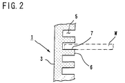
- a Si-SiC wafer boat for example, a vertical wafer boat 1 is constituted, as shown in Fig. 1, by assembling a bottom plate 2, strut 3, and top plate 4 formed of a Si-SiC base material.
- the strut 3 which has, for example, a square section, is stood by four on the bottom plate 2, and a support part 6 for loading a semiconductor wafer W is formed on each strut 3.
- the support part 6 has a support groove 5 longitudinally formed in comb-tooth shape as shown in Fig. 2.
- the Si-SiC wafer boat base material consisting of the bottom plate, strut and top plate has ultra-high purity with a Fe content of 0.05 ppm or less and a total content of Ni, Cu, Na, Ca, Cr and K of 0.1 ppm or less as the metal impurity content.
- the reason of setting the Fe content of the base material to 0.05 ppm or less and the total content of typical contained metals to 0.1 ppm or less is to prevent the semiconductor wafer W from being metal-contaminated even if no CVD-SiC film is formed on the base material in the heat treatment of the semiconductor wafer W by use of the wafer boat 1.
- the semiconductor wafer W is remarkably metal-contaminated in the heat treatment of the semiconductor wafer W by use of the wafer boat 1.
- the reason of setting the surface roughness (Ra) of the part to make contact with the semiconductor wafer W of the wafer boat 1 is to prevent the occurrence of slip on the surface of the semiconductor wafer W in the heat treatment of the semiconductor wafer W by use of the wafer boat 1.
- a surface roughness (Ra) exceeding 0.20 ⁇ m causes the slip on the surface of the semiconductor wafer W in the heat treatment of the semiconductor wafer W by use of the wafer boat 1.
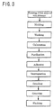
- the Si-SiC wafer boat 1 having the structure as described above can be produced according to a process flow as shown in Fig. 3.
- the producing process of the wafer board comprises the kneading step of kneading a SiC powder having a total metal impurity quantity of 0.2 ppm or less with a molding assistant; the molding step of molding the kneaded raw material into a bottom plate compact 2p, a strut compact 3p and a top plate compact 4p; the step of working the compacts 2p, 3p, 4p; the step of calcining the worked compacts 2p, 3p, 4p; the purifying step of purifying the calcined compacts 2t, 3t, 4t in halogen gas-containing atmosphere at 1900-2000°C; the adhering step of adhering the resulting purified bodies 2t, 3t, 4t by use of an adhesive; the impregnating step of impregnating the adhesively formed wafer boat purified body 1t with silicon followed by heating; the step of grinding the wafer boat 1 impregnated with silicon; the grooving step of forming a plurality
- the compacts 2p, 3p, 4p are heated for about 2 hours under an ordinary condition, for example, in Ar gas atmosphere at 1500-2000°C, to provide the calcined bodies 2t, 3t, 4t.
- the wafer boat purified body 1t assembled by adhering the purified bodies 2t, 3t, 4t is transferred to the silicon-impregnating step as shown in Fig. 4.
- the wafer boat calcined body 1t is housed in a porous carbon-made sealed vessel 9 with a porosity of 7-20% provided within an induction heating furnace body 8 and kept cleanly.
- the wafer boat purified body 1t housed in the sealed vessel 9 is placed in the separated state from a fused silicon S consisting of heated and fused polysilicon above a fused silicon tank 10 containing the fused silicon S, and a heat-resisting capillary tube body 11 having one end dipped in the fused silicon S and the other end mounted on the wafer boat compact 1t is used to impregnate the fused silicon S to the waver boat compact 1t while energizing and moving an induction heating coil 12.
- the impregnation of the purified body 1t is performed by use of the sealed vessel 9 provided within the induction heating furnace body 8, whereby the metal contamination of the wafer board 1 impregnated with Si can be prevented.
- the cutting is performed by use of a diamond blade to form the wafer-supporting support grooves 5 on the strut 3 of the wafer boat 1.
- the use of the diamond blade allows the upper surface 7 of the cut support part 6 to have a surface roughness of Ra ⁇ O.20 ⁇ m, which is not larger than that of the CVD-SiC film surface.
- the ultra-high purity base material is used for the wafer boat 1, and the part to make contact with the semiconductor wafer W is extremely flattened into a surface roughness of 0.20 ⁇ m or less, as described above, the semiconductor wafer W is never contaminated even if no CVD-SiC film is formed on the base material surface, nor slip is caused. Since no CVD-SiC film is formed, a strict washing for removing the metal impurities segregated on the surface of the SiC film is not required.
- a single-wafer-processing susceptor 21 is suitable for a wafer with a large diameter as a semiconductor wafer having a diameter of 300 mm, and it is formed of a disc-like susceptor body 22 and a housing recessed part 23 provided on the susceptor body 22 to house a semiconductor wafer W.
- the base material for forming the susceptor body 21 has a Fe content of 0.05 ppm or less and a total content of Ni, Cu, Na, Ca, Cr and K of 0.1 ppm or less as the metal impurity content, and also has a surface roughness (Ra) of 0.20 ⁇ m or less in the part to make contact with the semiconductor wafer W, for example, the surface 24 of the housing recessed part 23.
- the above single-wafer-processing susceptor 21 can be produced in the same method as the above-described wafer boat of the typical example.
- Avertical wafer boat as a typical example of the second embodiment of the Si-SiC member for heat treatment of semiconductor according to this invention is described below in reference to the drawings.
- the Si-SiC vertical wafer boat 31 of the second embodiment has the same form as the wafer boat of the first embodiment shown in Fig. 1, and it is formed of a Si-SiC base material.
- the wafer boat 31 is formed by assembling a bottom plate (not shown), strut 32 and top plate (not shown) formed of the Si-SiC base material as shown in Fig. 6.
- the Si-SiC wafer boat base material consisting of the bottom plate, strut 32 and top plate has ultra-high purity with a Fe content of 0.05 ppm or less a total content of Ni, Cu, Na, Ca, Cr and K of 0.1 ppm or less as the metal impurity content.
- a CVD film 34 having a prescribed thickness, for example, 30-100 ⁇ m, is formed on the surface 33 of the base material for forming the bottom plate, strut 32 and top plate as shown in Fig. 7, and the content of Fe and Na is held to 300 ppb or less in the area at least a depth t of 10 ⁇ m from the surface 35 of the CVD film 34.
- the reason of setting the Fe content of the base material to 0.05 ppm or less and the total content of other typical contained metals to 0.1 ppm or less is to prevent the semiconductor wafer W from being contaminated with the metal impurities segregated from the base onto the surface of the CVD-SiC film in the heat treatment of the semiconductor wafer W by use of the wafer boat 31.
- the metal impurities are segregated on the surface of the SiC film even if the CVD-SiC film is formed on the surface of the SiC film, and the semiconductor wafer W is metal-contaminated in the heat treatment of the semiconductor wafer W.
- the reason of setting the surface roughness (Ra) of the part to make contact with the semiconductor wafer W of the wafer boat 31 to 0.20 ⁇ m or less is that the surface roughness of the CVD-SiC film is significantly influenced by the surface roughness of the base material.
- the surface roughness (Ra) of the CVD-SiC film also exceeds 0.20 ⁇ m to cause a slip on the surface of the semiconductor wafer W in the heat treatment of the semiconductor wafer W.
- the reason of setting the content of Fe and Na to 300 ppb or less in the area of at least a depth t of 10 ⁇ m from the surface 35 of the CVD film 34 is that the diffusion of the metal impurities to the part to make contact with the semiconductor wafer W can be minimized, so that the contamination of the semiconductor wafer W can be prevented in the heat treatment of the semiconductor wafer W.
- the semiconductor wafer W is contaminated with the Fe and Na contained in the CVD film 34 in the heat treatment of the semiconductor wafer W.
- the Si-SiC wafer boat 31 of the second embodiment can be produced also according to the process flow shown in Fig. 3 similarly to the production of the Si-SiC wafer boat 1 of the first embodiment.
- the CVD film 34 having a thickness, for example, 30 ⁇ m-lOO ⁇ m is formed according to an ordinary CVD method.
- the wafer boat 31 having the CVD film 34 formed thereon is washed and completed.
- the ultra-high purity base material is used for the wafer boat 31, the part to make contact with the semiconductor wafer W is extremely flattened, and the CVD-SiC film is formed on the base material surface, as described above, the contamination of the semiconductor wafer W can be further prevented, and the occurrence of the slip can be also suppressed.
- the segregation of metal impurities onto the surface of the SiC film can be eliminated by use of the ultra-high purity base material, and the strict washing can be dispensed with.
- a single-wafer-processing susceptor having the CVD film formed thereon is considerable.
- the metal impurity content of the wafer boat base material is measured.
- Example 1 An acrylic binder, which is a molding assistant, was added to an ultra-high purity SiC powder (total metal impurity quantity of 0.2 ppm or less) having the average particle size and metal impurity content shown in Table 1 followed by kneading to produce a test piece compact having a section of 2 cm x 2 cm and a length of 30 cm by casting.
- the compact was baked (calcined) at 1700°C for about 2 hours in argon atmosphere, and then purified at 1900°C in halogen gas-containing atmosphere to provide a test piece.
- the test piece purified body was placed in a high purity carbon sealed vessel with a porosity of 13% provided within an induction heating furnace body to provide a test piece impregnated body impregnated with fused silicon.
- Comparative Example 1 A test piece impregnated body was produced in the same manner as the above example except using a SiC powder having the average particle size and metal impurity content shown in Table 1 (total metal impurity quantity exceeding 0.2 ppm) and adapting a conventional impregnating method using no sealed vessel in the impregnating step.
- Example 1 and Comparative Example 1 obtained in the above (1) were partially cut, and the solutions thereof extracted with acid were subjected to a measurement by ICP emission spectral analysis.
- Example 1 even the Fe content, which is the highest therein, is as small as 0.02 ppm, and the contents of all other metals are 0.01 ppm or less, which shows that the test piece of Example 1 has extremely ultra-high purity.
- the Fe content in Comparative Example 1 is 0.27 ppm, which is 13.5 times Example 1, and the contents of the other metals are also 3-6 times the Example.
- the surface roughness of the support groove to make contact with a semiconductor wafer is measured.
- Example 2 An acrylic binder, which is a molding assistant, was added to an ultra-high purity SiC powder (total metal impurity quantity of 0.2 ppm or less) having the average particle size and metal impurity content as shown in Table 1 followed by kneading to produce a bottom plate compact, a strut compact and a top plate compact by casting.
- the resulting compacts were adhered by use of an adhesive (obtained by adding a phenolic binder to a mixed powder consisting of silicon carbide powder and carbon powder) to assemble a boat compact.
- the boat compact was baked (calcined) at 1700°C for about 2 hours in argon atmosphere, and then purified at 1950°C in halogen gas-containing atmosphere to provide a boat purified body.
- the boat purified body was placed in a high purity carbon-made sealed vessel with a porosity of 15% provided within an induction heating furnace body to provide a wafer boat impregnated body impregnated with fused silicon under reduced pressure.
- the induction heating furnace body was provided with a mechanism for introducing N 2 gas, which is an inert gas, from one furnace wall and discharging the N 2 gas from the other furnace wall by a vacuum pump.
- a support groove was formed on the wafer boat impregnated body by use of a diamond blade to provide a wafer boat for 8-inch wafer.
- Comparative Examples 2-3 By use of a high purity SiC powder having the average particle size and metal impurity content as shown in Table 2 (total metal impurity quantity exceeding 0.2 ppm), a wafer boat for 8-inch wafer was provided in the same manner as Example 2 [Comparative Example 2 (base material)]. In the silicon-impregnating step, a conventional method of impregnating silicon on a heater induction-heated by a movable high frequency coil was adapted. Further, a SiC film was formed on the wafer boat by CVD [Comparative Example 3 (with film)]. The purifying treatment was performed according to a conventional method, and the support groove was formed by use of a conventional cutting tool.
- the support piece having the support groove formed thereon was cut from each of Example 2 and Comparative Example 3 (with film) obtained in the above (1), and the surface roughness was measured for the surface for supporting a semiconductor wafer by use of a surface roughness measuring machine.
- Example 2 The surface roughness of Example 2 is as extremely flat as 0.12 ⁇ m, compared with 0.45 ⁇ m of Comparative Example 3 (with film).
- the metal impurity quantity transferred to a semiconductor wafer during heat treatment is measured by use of a wafer boat.
- One 8-inch silicon wafer was loaded on each of the wafer boats [Example 2, Comparative Example 2 (base material), Comparative Example 3 (with film)], and heated at 1100°C in N 2 /O 2 atmosphere to measure the metal impurities transferred onto the silicon wafer surface.
- the transferred quantity in Example 2 is smaller than in Comparative Example 3 (with film) for the metals other than Ni and Ca. Compared with Comparative Example 2 (base material) having no CVD film, the transfer quantity is as small as about 1/5-1/2 for all the metals.
- Example 2 and Comparative Example 3 (with film) obtained in the above [2](1), three in total of 8-inch silicon wafers were loaded one by one, the temperature was raised at a prescribed speed to 1200°C, this temperature was held for 1 hour, and the silicon wafers were thereafter taken out to observe the state of occurrence of slip by use of a differential interference microscope.
- Example 4 The production was performed in the same manner as Example 3 except performing the Si impregnation within a high purity glass carbon vessel with a porosity of 0.5 %.
- Example 5 The production was performed in the same manner as Example 3 except performing the Si impregnation within a high purity carbon vessel with a porosity of 30%.
- Test pieces were cut from the Si-impregnated boat impregnation bodies impregnated with Si according to the respective methods.
- the metal impurity contents of the base materials impregnated with Si by use of Examples 3-5 are remarkably lower than the metal impurity content of the base material impregnated by use of Comparative Example 4.
- Example 4 using the high purity glass carbon vessel with porosity of 0.5% as the sealed vessel and Example 5 using the high purity carbon vessel with porosity of 30% than in Example 3 using the high purity carbon vessel with porosity of 15%.
- the metal impurity content of a wafer boat base material having a CVD film formed thereon is measured.
- Example 6 A wafer boat for heat treatment of 8-inch wafer having the metal impurity content shown in Table 7 was produced in the same manner as Example 2 of the above [2](1). This base material was placed in an atmosphere mainly composed of silane gas at 1100°C to form a SiC film by CVD method (Example 6). In the production of this wafer boat, a small sample of the same ultra-high purity base material as the wafer boat was also placed therein to form the CVD film.
- Comparative Example 5 A wafer boat for heat treatment of 8-inch wafer having the metal impurity content shown in Table 7 was produced in the same manner as Comparative Example 4 described above. A CVD-SiC film was formed on this base material in the same manner as Example 6 (Comparative Example 5). In the production of this wafer boat, a small sample of the same ultra-high purity base material as the wafer boat was placed to form the CVD film.
- Example 6 By use of Example 6 and Comparative Example 5 obtained in the above (1), a wafer evaluation (semiconductor evaluation) as described below was performed.
- Fig. 11 shows one example of the sealed vessel.
- the sealed vessel 51 has no hole extending through the thickness direction of the base material constituting it.
- the side part of the sealed vessel 51 is opened, and it is closable by a lid 52.
- Denoted at 53 is the fitting part of the lid 52.
- the purified body of the SiC member is taken out and in through this part.
- Fig. 12 shows one example of the internal structure of the heating furnace.
- the sealed vessel 51 is arranged within a furnace body 61, so that the inert gas can be sufficiently carried as shown by the arrow. Consequently, the vapor leaving through the pore part of the sealed vessel 51 is efficiently discharged.
- the method for producing a Si-SiC member for heat treatment of semiconductor according to this invention allows to provide a Si-SiC member reduced in the metal contamination to a semiconductor (wafer) to be heated as much as possible.
- the working step of setting the surface roughness (Ra) of the part to make contact with the semiconductor in the Si-SiC member for heat treatment of semiconductor to 0.20 ⁇ m or less is added, whereby the occurrence of slip in the heat treatment of a semiconductor wafer with a large diameter of 8 inches or more at high temperature can be reduced as much as possible.
- Average Particle Size and Metal Impurity Content of Raw Material Powder ppm
- Ultra-High Purity SiC 40 0.05 ⁇ 0.01 ⁇ 0.01 0.01 0.02 0.01 0.01 10 0.04 0.02 ⁇ 0.01 ⁇ 0.01 0.03 ⁇ 0.01 ⁇ 0.01 C.
Applications Claiming Priority (1)
| Application Number | Priority Date | Filing Date | Title |
|---|---|---|---|
| PCT/JP2000/000840 WO2001060764A1 (fr) | 2000-02-15 | 2000-02-15 | PROCEDE DE FABRICATION D'ELEMENT Si-SiC POUR TRAITEMENT THERMIQUE DE SEMI-CONDUCTEURS |
Publications (3)
| Publication Number | Publication Date |
|---|---|
| EP1184355A1 true EP1184355A1 (fr) | 2002-03-06 |
| EP1184355A4 EP1184355A4 (fr) | 2006-04-05 |
| EP1184355B1 EP1184355B1 (fr) | 2006-12-13 |
Family
ID=11735687
Family Applications (1)
| Application Number | Title | Priority Date | Filing Date |
|---|---|---|---|
| EP00902988A Expired - Lifetime EP1184355B1 (fr) | 2000-02-15 | 2000-02-15 | PROCEDE DE FABRICATION D'ELEMENT Si-SiC POUR TRAITEMENT THERMIQUE DE SEMI-CONDUCTEURS |
Country Status (4)
| Country | Link |
|---|---|
| US (1) | US6699401B1 (fr) |
| EP (1) | EP1184355B1 (fr) |
| DE (1) | DE60032358T2 (fr) |
| WO (1) | WO2001060764A1 (fr) |
Cited By (4)
| Publication number | Priority date | Publication date | Assignee | Title |
|---|---|---|---|---|
| WO2004095545A2 (fr) * | 2003-03-28 | 2004-11-04 | Saint-Gobain Ceramics & Plastics, Inc. | Support de plaquettes presentant des caracteristiques de traitement ameliorees |
| WO2005068395A2 (fr) * | 2004-01-06 | 2005-07-28 | Saint-Gobain Ceramics & Plastics, Inc. | Articles en carbure de silicium de purete elevee et procedes |
| EP1620878A2 (fr) * | 2003-04-15 | 2006-02-01 | Saint-Gobain Ceramics and Plastics, Inc. | Procede de traitement de composants de transformation de semi-conducteurs et composants obtenus par ce procede |
| WO2009085703A2 (fr) * | 2007-12-20 | 2009-07-09 | Saint-Gobain Ceramics & Plastics, Inc. | Procédé de traitement de composants de traitement de semi-conducteurs et composants ainsi formés |
Families Citing this family (10)
| Publication number | Priority date | Publication date | Assignee | Title |
|---|---|---|---|---|
| JP2002270614A (ja) * | 2001-03-12 | 2002-09-20 | Canon Inc | Soi基体、その熱処理方法、それを有する半導体装置およびその製造方法 |
| JP4136380B2 (ja) * | 2001-12-21 | 2008-08-20 | 日本碍子株式会社 | 高熱伝導性含Si材料及びその製造方法 |
| US7888685B2 (en) * | 2004-07-27 | 2011-02-15 | Memc Electronic Materials, Inc. | High purity silicon carbide structures |
| US8017062B2 (en) * | 2004-08-24 | 2011-09-13 | Yeshwanth Narendar | Semiconductor processing components and semiconductor processing utilizing same |
| EP1855312B1 (fr) * | 2005-02-22 | 2014-04-09 | Hitachi Metals, Ltd. | PROCÉDÉ DE FABRICATION D UN SUBSTRAT DE MONOCRISTAL EN SiC |
| US8633483B2 (en) * | 2007-06-26 | 2014-01-21 | Massachusetts Institute Of Technology | Recrystallization of semiconductor wafers in a thin film capsule and related processes |
| US8261730B2 (en) * | 2008-11-25 | 2012-09-11 | Cambridge Energy Resources Inc | In-situ wafer processing system and method |
| KR101854731B1 (ko) * | 2011-07-28 | 2018-05-04 | 엘지이노텍 주식회사 | 잉곳 제조 방법 |
| KR101429139B1 (ko) * | 2013-05-06 | 2014-08-13 | 한국내화 주식회사 | 고로 스테이브용 규소-탄화규소 충진재 |
| CN112786500A (zh) * | 2019-11-11 | 2021-05-11 | 夏泰鑫半导体(青岛)有限公司 | 晶圆架及具有晶圆架的垂直晶舟 |
Family Cites Families (18)
| Publication number | Priority date | Publication date | Assignee | Title |
|---|---|---|---|---|
| DE6913124U (de) | 1968-12-24 | 1970-11-19 | Ford Werke Ag | Kupplungsstueck fuer elektrische leitungen, insbesondere in kraftfahrzeugen |
| JP2573480B2 (ja) | 1985-11-22 | 1997-01-22 | 東芝セラミックス 株式会社 | 半導体熱処理用治具 |
| JPH0521297Y2 (fr) | 1986-07-31 | 1993-06-01 | ||
| JPS6335452A (ja) | 1986-07-31 | 1988-02-16 | 東芝セラミツクス株式会社 | 半導体拡散炉用構成部材の製造方法 |
| JPS6436981A (en) | 1987-07-31 | 1989-02-07 | Mazda Motor | Ignitor for engine |
| JP2548949B2 (ja) * | 1987-09-01 | 1996-10-30 | 東芝セラミックス株式会社 | 半導体製造用構成部材 |
| JPH0784351B2 (ja) | 1990-11-20 | 1995-09-13 | 旭硝子株式会社 | 半導体熱処理装置および半導体熱処理装置用高純度炭化珪素質部材とその製造方法 |
| EP0486938B1 (fr) | 1990-11-20 | 1999-05-19 | Asahi Glass Company Ltd. | Appareil pour le traitement thermique des semi-conducteurs et pièces en carbure de silicium ayant une pureté élevée pour l'appareil et procédé de leur fabrication |
| JP2973762B2 (ja) | 1993-01-18 | 1999-11-08 | 住友金属工業株式会社 | 半導体製造用炭化珪素焼結体の製造方法 |
| US5589116A (en) * | 1991-07-18 | 1996-12-31 | Sumitomo Metal Industries, Ltd. | Process for preparing a silicon carbide sintered body for use in semiconductor equipment |
| CA2099788A1 (fr) | 1992-07-31 | 1994-02-01 | Michael A. Pickering | Carbure de silicium ultra pur et installation de traitement haute temperature pour semi-conducteur |
| US5374412A (en) | 1992-07-31 | 1994-12-20 | Cvd, Inc. | Highly polishable, highly thermally conductive silicon carbide |
| JP3276429B2 (ja) | 1992-11-27 | 2002-04-22 | 東芝セラミックス株式会社 | 半導体ウエハ処理部材 |
| JP2950122B2 (ja) * | 1993-07-29 | 1999-09-20 | 信越化学工業株式会社 | セラミックスと金属との複合体の製造方法及び製造装置 |
| GB2301545B (en) * | 1995-06-02 | 1999-04-28 | Aea Technology Plc | The manufacture of composite materials |
| JP3469688B2 (ja) | 1995-10-13 | 2003-11-25 | 東芝セラミックス株式会社 | 半導体熱処理用部材の製造方法 |
| JP3642446B2 (ja) | 1996-08-01 | 2005-04-27 | 東芝セラミックス株式会社 | 半導体ウエハ処理具 |
| JPH118216A (ja) | 1997-06-16 | 1999-01-12 | Toshiba Ceramics Co Ltd | 半導体製造用部材の洗浄方法 |
-
2000
- 2000-02-15 WO PCT/JP2000/000840 patent/WO2001060764A1/fr active IP Right Grant
- 2000-02-15 EP EP00902988A patent/EP1184355B1/fr not_active Expired - Lifetime
- 2000-02-15 US US09/958,911 patent/US6699401B1/en not_active Expired - Fee Related
- 2000-02-15 DE DE60032358T patent/DE60032358T2/de not_active Expired - Fee Related
Non-Patent Citations (2)
| Title |
|---|
| No further relevant documents disclosed * |
| See also references of WO0160764A1 * |
Cited By (10)
| Publication number | Priority date | Publication date | Assignee | Title |
|---|---|---|---|---|
| WO2004095545A2 (fr) * | 2003-03-28 | 2004-11-04 | Saint-Gobain Ceramics & Plastics, Inc. | Support de plaquettes presentant des caracteristiques de traitement ameliorees |
| WO2004095545A3 (fr) * | 2003-03-28 | 2005-05-12 | Saint Gobain Ceramics | Support de plaquettes presentant des caracteristiques de traitement ameliorees |
| EP1620878A2 (fr) * | 2003-04-15 | 2006-02-01 | Saint-Gobain Ceramics and Plastics, Inc. | Procede de traitement de composants de transformation de semi-conducteurs et composants obtenus par ce procede |
| EP1620878A4 (fr) * | 2003-04-15 | 2008-03-26 | Saint Gobain Ceramics | Procede de traitement de composants de transformation de semi-conducteurs et composants obtenus par ce procede |
| WO2005068395A2 (fr) * | 2004-01-06 | 2005-07-28 | Saint-Gobain Ceramics & Plastics, Inc. | Articles en carbure de silicium de purete elevee et procedes |
| WO2005068395A3 (fr) * | 2004-01-06 | 2005-10-06 | Saint Gobain Ceramics | Articles en carbure de silicium de purete elevee et procedes |
| US7501370B2 (en) | 2004-01-06 | 2009-03-10 | Saint-Gobain Ceramics & Plastics, Inc. | High purity silicon carbide wafer boats |
| WO2009085703A2 (fr) * | 2007-12-20 | 2009-07-09 | Saint-Gobain Ceramics & Plastics, Inc. | Procédé de traitement de composants de traitement de semi-conducteurs et composants ainsi formés |
| WO2009085703A3 (fr) * | 2007-12-20 | 2009-10-22 | Saint-Gobain Ceramics & Plastics, Inc. | Procédé de traitement de composants de traitement de semi-conducteurs et composants ainsi formés |
| US8058174B2 (en) | 2007-12-20 | 2011-11-15 | Coorstek, Inc. | Method for treating semiconductor processing components and components formed thereby |
Also Published As
| Publication number | Publication date |
|---|---|
| US6699401B1 (en) | 2004-03-02 |
| DE60032358D1 (de) | 2007-01-25 |
| WO2001060764A1 (fr) | 2001-08-23 |
| EP1184355B1 (fr) | 2006-12-13 |
| EP1184355A4 (fr) | 2006-04-05 |
| DE60032358T2 (de) | 2007-10-25 |
Similar Documents
| Publication | Publication Date | Title |
|---|---|---|
| US6699401B1 (en) | Method for manufacturing Si-SiC member for semiconductor heat treatment | |
| JP5281027B2 (ja) | 半導体加工用部品を処理する方法とこの方法によって形成される部品 | |
| US4040849A (en) | Polycrystalline silicon articles by sintering | |
| KR100953707B1 (ko) | 반도체 프로세싱 부품 및 이를 사용하는 반도체 제조방법 | |
| EP0486938B1 (fr) | Appareil pour le traitement thermique des semi-conducteurs et pièces en carbure de silicium ayant une pureté élevée pour l'appareil et procédé de leur fabrication | |
| EP0826646B1 (fr) | Produit en carbure de silicium ayant une résistance à la corrosion élevée | |
| KR100756619B1 (ko) | 질화알루미늄 소결체, 반도체 제조용 부재 및 질화알루미늄소결체의 제조 방법 | |
| KR100592741B1 (ko) | 탄화규소성형체 | |
| WO2005068395A2 (fr) | Articles en carbure de silicium de purete elevee et procedes | |
| EP0340802B1 (fr) | Tuyau de diffusion en carbure de silicium pour semi-conducteur | |
| JPH08188468A (ja) | 化学蒸着法による炭化ケイ素成形体及びその製造方法 | |
| JPH1012692A (ja) | ダミーウエハ | |
| JPH08188408A (ja) | 化学蒸着法による炭化ケイ素成形体及びその製造方法 | |
| JP4798693B2 (ja) | プラズマ処理装置用イットリアセラミックス部品及びその製造方法 | |
| JP2000119079A (ja) | 半導体熱処理用Si−SiC製部材およびその製造方法 | |
| JPH09275078A (ja) | シリコンウエハ保持治具 | |
| JP3642446B2 (ja) | 半導体ウエハ処理具 | |
| JP4382919B2 (ja) | シリコン含浸炭化珪素セラミックス部材の製造方法 | |
| JP3145518B2 (ja) | 表面高純度セラミックス及びその製造方法 | |
| US6071343A (en) | Heat treatment jig and method of producing the same | |
| JP4421251B2 (ja) | Dlc膜およびこれを備えた真空チャック | |
| JPH11279761A (ja) | 耐食性部材 | |
| JP3685365B2 (ja) | 半導体装置部材用の精製炭化珪素粉末とその精製方法、及び該粉末から得られる半導体装置部材用焼結体の製造方法 | |
| JPH11278944A (ja) | 窒化珪素質耐食性部材及びその製造方法 | |
| JP2023545369A (ja) | ジルコニア強化アルミナセラミック焼結体 |
Legal Events
| Date | Code | Title | Description |
|---|---|---|---|
| PUAI | Public reference made under article 153(3) epc to a published international application that has entered the european phase |
Free format text: ORIGINAL CODE: 0009012 |
|
| 17P | Request for examination filed |
Effective date: 20010427 |
|
| AK | Designated contracting states |
Kind code of ref document: A1 Designated state(s): DE FR GB |
|
| A4 | Supplementary search report drawn up and despatched |
Effective date: 20060221 |
|
| GRAP | Despatch of communication of intention to grant a patent |
Free format text: ORIGINAL CODE: EPIDOSNIGR1 |
|
| GRAS | Grant fee paid |
Free format text: ORIGINAL CODE: EPIDOSNIGR3 |
|
| GRAA | (expected) grant |
Free format text: ORIGINAL CODE: 0009210 |
|
| AK | Designated contracting states |
Kind code of ref document: B1 Designated state(s): DE FR GB |
|
| REG | Reference to a national code |
Ref country code: GB Ref legal event code: FG4D |
|
| REF | Corresponds to: |
Ref document number: 60032358 Country of ref document: DE Date of ref document: 20070125 Kind code of ref document: P |
|
| ET | Fr: translation filed | ||
| PLBE | No opposition filed within time limit |
Free format text: ORIGINAL CODE: 0009261 |
|
| STAA | Information on the status of an ep patent application or granted ep patent |
Free format text: STATUS: NO OPPOSITION FILED WITHIN TIME LIMIT |
|
| 26N | No opposition filed |
Effective date: 20070914 |
|
| REG | Reference to a national code |
Ref country code: GB Ref legal event code: 732E |
|
| REG | Reference to a national code |
Ref country code: FR Ref legal event code: TP |
|
| PGFP | Annual fee paid to national office [announced via postgrant information from national office to epo] |
Ref country code: DE Payment date: 20090213 Year of fee payment: 10 |
|
| PGFP | Annual fee paid to national office [announced via postgrant information from national office to epo] |
Ref country code: GB Payment date: 20090211 Year of fee payment: 10 |
|
| PGFP | Annual fee paid to national office [announced via postgrant information from national office to epo] |
Ref country code: FR Payment date: 20090213 Year of fee payment: 10 |
|
| GBPC | Gb: european patent ceased through non-payment of renewal fee |
Effective date: 20100215 |
|
| REG | Reference to a national code |
Ref country code: FR Ref legal event code: ST Effective date: 20101029 |
|
| PG25 | Lapsed in a contracting state [announced via postgrant information from national office to epo] |
Ref country code: FR Free format text: LAPSE BECAUSE OF NON-PAYMENT OF DUE FEES Effective date: 20100301 |
|
| PG25 | Lapsed in a contracting state [announced via postgrant information from national office to epo] |
Ref country code: DE Free format text: LAPSE BECAUSE OF NON-PAYMENT OF DUE FEES Effective date: 20100901 |
|
| PG25 | Lapsed in a contracting state [announced via postgrant information from national office to epo] |
Ref country code: GB Free format text: LAPSE BECAUSE OF NON-PAYMENT OF DUE FEES Effective date: 20100215 |