EP1168628B1 - Current adding type D/A converter - Google Patents
Current adding type D/A converterInfo
- Publication number
- EP1168628B1 EP1168628B1 EP01115464A EP01115464A EP1168628B1 EP 1168628 B1 EP1168628 B1 EP 1168628B1 EP 01115464 A EP01115464 A EP 01115464A EP 01115464 A EP01115464 A EP 01115464A EP 1168628 B1 EP1168628 B1 EP 1168628B1
- Authority
- EP
- European Patent Office
- Prior art keywords
- current
- cells
- current cell
- cell
- sequence
- Prior art date
- Legal status (The legal status is an assumption and is not a legal conclusion. Google has not performed a legal analysis and makes no representation as to the accuracy of the status listed.)
- Expired - Lifetime
Links
Images


Classifications
-
- H—ELECTRICITY
- H03—ELECTRONIC CIRCUITRY
- H03M—CODING; DECODING; CODE CONVERSION IN GENERAL
- H03M1/00—Analogue/digital conversion; Digital/analogue conversion
- H03M1/06—Continuously compensating for, or preventing, undesired influence of physical parameters
- H03M1/0617—Continuously compensating for, or preventing, undesired influence of physical parameters characterised by the use of methods or means not specific to a particular type of detrimental influence
- H03M1/0634—Continuously compensating for, or preventing, undesired influence of physical parameters characterised by the use of methods or means not specific to a particular type of detrimental influence by averaging out the errors, e.g. using sliding scale
- H03M1/0656—Continuously compensating for, or preventing, undesired influence of physical parameters characterised by the use of methods or means not specific to a particular type of detrimental influence by averaging out the errors, e.g. using sliding scale in the time domain, e.g. using intended jitter as a dither signal
- H03M1/066—Continuously compensating for, or preventing, undesired influence of physical parameters characterised by the use of methods or means not specific to a particular type of detrimental influence by averaging out the errors, e.g. using sliding scale in the time domain, e.g. using intended jitter as a dither signal by continuously permuting the elements used, i.e. dynamic element matching
-
- H—ELECTRICITY
- H03—ELECTRONIC CIRCUITRY
- H03M—CODING; DECODING; CODE CONVERSION IN GENERAL
- H03M1/00—Analogue/digital conversion; Digital/analogue conversion
- H03M1/66—Digital/analogue converters
- H03M1/74—Simultaneous conversion
- H03M1/742—Simultaneous conversion using current sources as quantisation value generators
- H03M1/747—Simultaneous conversion using current sources as quantisation value generators with equal currents which are switched by unary decoded digital signals
Definitions
- the present invention relates to a current adding type D/A converter equipped with a plurality of current cells made by employing constant current sources, and more specifically, is related to an improvement in a differential linearity error occurred in the D/A converter.
- Fig. 9 is an explanatory diagram for showing an arranging structural example of current cells of the current adding type D/A converter. This example indicates such a case that a total number of current cells is equal to 16.
- Fig. 9(A) shows an array sequence of the current cells
- Fig. 9(B) represents a switching sequence of the current cells.
- a current cell 501 through a current cell 516 are made of the same current cells.
- each of these current cells is constituted by employing a constant current source and a switch used to turn ON this constant current source.
- These current cells are arranged in the form of, for example, one column in this order of reference numerals 501 to 516.
- These reference numerals 501 to 516 correspond to array numbers of the current cells.
- numerals [1] to [16] denoted on the respective current cells in Fig. 9(A) correspond to switching numbers, namely represent such a sequence that the current cells are switched.
- Fig. 9(B) shows current cells which are arranged by rearranging the above-described current cells of Fig. 9(A) in another switching order as shown in Fig. 9(B). Reference numerals denoted in the respective current cells show array numbers.
- the current cell 510, the current cell 502, the current cell 511, the current cell 503, the current cell 512, the current cell 504, the current cell 513, the current cell 505, the current cell 514, the current cell 506, the current cell 515, the current cell 507, and the current cell 516 are sequentially turned ON, so that output currents from the current cells are added to each other.
- the current cell 508 is turned ON, so that since all of the 16 current cells are turned ON, the maximum current may flow.
- the summation of the current amounts flowing from a plurality of current cells is controlled.
- This current is converted into a voltage by an output resistor, so that the D/A converting operation as to the input data is carried out.
- the analog output signal can be obtained with respect to the digital input data.
- Fig. 10 is a graphic representation for representing a differential linearity error occurred in the case that the respective current cells are switched in the switching sequence shown in Fig. 9.
- such differential linearity errors are indicated every output value when 1LSB is selected to be 1 in such a case that the output current amounts of the respective current cells are changed by 1 % due to the cell arrangement.
- an ordinate indicates a magnitude of the differential linearity errors.
- An abscissa indicates a magnitude of total output current amounts (namely, total number of current cells which are turned ON and correspond to magnitude of input data).
- the differential linearity errors are made uniform over the entire output range.
- the entire differential linearity error can be made substantially uniform by switching the current cells in the discrete manner.
- the precision with respect to the input data in the vicinity of the normally-used center point (namely, intermediate point between maximum value and minimum value) is made substantially identical to the precision with respect to the input data in the vicinity of both the maximum value and the minimum value, whose use frequency degrees are low.
- the differential linearity errors occurred in the vicinity of the center point are large, especially, which may constitute the major factor of the D/A converter performance.
- the present invention has been made to solve the above-explained problems, and therefore, has an object to provide such a current adding type D/A converter capable of improving characteristics thereof in the normally-used range such as while a signal has a small amplitude.
- the D/A converter according to the present invention is capable of reducing differential linearity errors occurred in the vicinity of a center point of input data.
- a current adding type D/A converter is featured by that in such a current adding type D/A converter having a plurality of current cells made by employing a plurality of constant current sources and a plurality of switches for turning ON the constant current sources, wherein: the current adding type D/A converter is comprised of switch control means; and wherein: in such a case that array numbers defined from “1" to "n” are applied to the plural current cells in the arranging order of the current cells, and the array number "n” is equal to the even number as well as "n/2” is equal to the even number, while combinations of the array numbers in which a summation of two array numbers becomes (n+1) are prepared within the plurality of current cells, an array of the array numbers is formed in such a manner that array numbers on the odd number side, or the even number side among the combinations of the current cells are arrayed from a smaller array number; and also the switch control means controls to turn ON the switches of the current cells in accordance with the array sequence, or another array sequence
- a current adding type D/A converter is featured by that in such a current adding type D/A converter having a plurality of current cells made by employing a plurality of constant current sources and a plurality of switches for turning ON the constant current sources, wherein: the current adding type D/A converter is comprised of switch control means; and wherein: in such a case that array numbers defined from “1" to "n” are applied to the plural current cells in the arranging order of the current cells, and the array number "n” is equal to the even number as well as "n/2" is equal to the odd number, while combinations of the array numbers in which a summation of two array numbers becomes (n+1) except for both the array number "1" and the array number "n” are prepared within the plurality of current cells, and further, the array number "1” is set as either a top number or a last number, an array of the array numbers is formed in such a manner that array numbers on the odd number side, or the even number side among the combinations of the current cells
- a current adding type D/A converter is featured by that in such a current adding type D/A converter having a plurality of current cells made by employing a plurality of constant current sources and a plurality of switches for turning ON the constant current sources, wherein: the current adding type D/A converter is comprised of switch control means; and wherein: in such a case that array numbers defined from “1" to "n” are applied to the plural current cells in the arranging order of the current cells, and the array number "n” is equal to the odd number as well as "(n+1)/2” is equal to the odd number, while combinations of the array numbers in which a summation of two array numbers becomes (n+1) except for the array number "(n+1)/2" are prepared within the plurality of current cells, an array of the array numbers is formed in such a manner that array numbers on the odd number side, or the even number side among the combinations of the current cells are arrayed from a smaller array number so as to form such an array that the array number (n+1
- a current adding type D/A converter is featured by that in such a current adding type D/A converter having a plurality of current cells made by employing a plurality of constant current sources and a plurality of switches for turning ON the constant current sources, wherein: the current adding type D/A converter is comprised of switch control means; and wherein: in such a case that array numbers defined from “1" to "n” are applied to the plural current cells in the arranging order of the current cells, and the array number "n” is equal to the odd number as well as "(n+1)/2” is equal to the even number, while combinations of the array numbers in which a summation of two array numbers becomes (n+1) except for the array number "1", the array number "n” and the array number "(n+1)/2” are prepared within the plurality of current cells, and further, the array number "1” is set as either a top number or a last number, an array of the array numbers is formed in such a manner that array numbers on the odd number side,
- a current adding type D/A converter is featured by that in the combinations of the current cells in which the summation of the two array numbers becomes (n+1), the combinations are arrayed by mutually and arbitrarily rearranging the sequences thereof.
- a current adding type D/A converter is featured by that in the case that the array number "n" is equal to the even number, the array of said current cells is divided by a power of "2" to obtain current cell groups, and the current cell groups which are located in symmetrical positions with respect to a center point of the array are arrayed by arbitrarily rearranging the sequences of the current cells in a symmetrical manner with respect to the center point.
- a current adding type D/A converter is featured by that in the case that the array number "n" is equal to the odd number, the array of the current cells is divided by a power of "2" except for the array number "(n+1)/2" to obtain current cell groups, and the current cell groups which are located in symmetrical positions with respect to a center point of the array are arrayed by arbitrarily rearranging the sequences of the current cells in a symmetrical manner with respect to the center point.
- the switching operation of the current cells is carried out as follows: That is, the switching sequence is determined in such a manner that the current cells having the large fluctuations of the output currents (namely, located on both sides) are turned ON in the order corresponding to such a value nearly equal to either the maximum value or the minimum value of the input data, whereas the current cells having the small fluctuations (located in the vicinity of center point) are turned ON in the order of such a value near the center point.
- a signal periodic signal such as audio signal
- a negative amplitude on the maximum value side and also on the minimum value side is employed while sandwiching a center point.
- the highest appearing frequency degree corresponds to the range in the vicinity of the center point of the input data.
- This range may correspond to such a normally-used range in which most of input data are concentrated.
- the precision of the D/A converter can be improved in the vicinity of the center point corresponding to the normally-used range in the general-purpose signal processing system, and also the distortions as well as the noise contained in the output signal can be decreased.
- Fig. 1 is an explanatory diagram for representing both an arranging construction and a switching sequence of current cells of a current adding type D/A converter according to a first embodiment mode of the present invention.
- Fig. 2 is a schematic block diagram for showing a structure of the current adding type D/A converter according to this first embodiment mode.
- the current adding type D/A converter is constituted by arranging a plurality of current cells 3. Each of these current cells 3 is constituted by employing a constant current source 1 and a switch 2 for controlling an output of this constant current source 1. Also, the current adding type D/A converter is provided with a switch control unit 4 for controlling the switch 2 of the above-explained current cell 3. This switch control unit 4 is connected to each of the current cells 3.
- the switches 2 of the respective current cells 3 are connected in such a manner that one terminals thereof are connected to the constant current sources 1, one ends of the other terminals are connected to each other, and these ends are collected to be connected to an output terminal 7. Other ends of the other terminals are similarly collected to each other and are connected to an inverting output terminal 8.
- An output resistor 5 is connected between a signal line of the output terminal 7, and the ground.
- An inverting resistor 6 is connected between a signal line of the output terminal 8 and the ground.
- the switch control unit 4 constructed of a decoder decodes data which is entered as D/A conversion input data, and switching-controls the switches 2 of the respective current cells 3 so as to operate the constant current source 1.
- this D/A converter performs D/A converting operation in such a manner that in response to a value of input data, a current is supplied from a preselected current cell 3 to both the output resistor 5 and the inverting output resistor 6 so as to be converted into a voltage. Then, an output signal defined by an analog voltage value is outputted from both the output terminal 7 and the inverting output terminal 8.
- Fig. 2 indicates such an arrangement equipped with both the inverting output terminal and the inverting output resistor, from which the current derived from the current cell under OFF state is outputted.
- these inverting output terminal and inverting output resistor are not provided, such a D/A converter having only one output may be arranged.
- Fig. 1(A) shows an array sequence of the current cells
- Fig. 1(B) represents a switching sequence of the current cells.
- a current cell 101 through a current cell 116 are made of the same current cells.
- each of these current cells is constituted by employing a constant current source and a switch used to turn ON this constant current source.
- These current cells are arranged in the form of, for example, one column in this order of reference numerals 101 to 116. These reference numerals 101 to 116 correspond to array numbers of the current cells. With respect to output current amounts of these current cells, it is so assumed that characteristics are changed at a constant inclination from the current cell 101 to the current cell 116.
- numerals [1] to [16] denoted on the respective current cells in Fig. 1(A) correspond to switching numbers, namely represent such a sequence that the current cells are switched.
- the current cells shown from the left-end current cell 101 to the right-end current cell 102 are turned ON in the sequential number defined from the switching number [1] to the switching number [16].
- Fig. 1(B) shows current cells which are arranged by rearranging the above-described current cells of Fig. 1(A) in another switching order as shown in Fig. 1(B).
- Reference numerals denoted in the respective current cells show array numbers.
- the current adding type D/A converter of this first embodiment mode is featured as follows: That is, when a total number of the current cells is equal to multiple number of "4", the turning-ON sequence of the current cells may cause differences in fluctuations of output current amounts to become constant as to two sets of adjoining current-cell groups (will also be referred to as "pair” hereinafter), and also may decrease output current characteristic changes in the vicinity of a center point of input data.
- this actual D/A converter when this actual D/A converter is formed by arranging the current cells from the current cell 101 up to the current cell 116, a process fluctuation may occur along a predetermined direction.
- the magnitudes of the output currents of the respective current cells are not always made constant. For example, assuming now that the output current amounts of these current cells are changed by 1 % per one current cell, there are errors of 15 % in the output current amount of the current cell 116 with respect to the current cell 101.
- the switching sequence is determined in such a manner that the current cells having the large fluctuations of the output currents (namely, located on both sides) are turned ON in the order corresponding to such a value nearly equal to either the maximum value or the minimum value, whereas the current cells having the small fluctuations (located in the vicinity of center point) are turned ON in the order of such a value near the center point.
- the characteristics such as the differential linearity errors can be improved because of the following reasons. That is, in the vicinity of the center point of the input data, the distances (namely, array numbers) among the current cells whose ON-sequences are continued are close positions, and the difference in the output current amounts every current cell becomes small.
- the following current cells constitute pair cells from the both ends of the current cell arrangement to the center, namely, both the current cell 101 and the current cell 116 constitute a pair; both the current cell 102 and the current cell 115 constitute a pair; both the current cell 103 and the current cell 114 constitute a pair; both the current cell 104 and the current cell 113 constitute a pair; both the current cell 105 and the current cell 112 constitute a pair; both the current cell 106 and the current cell 111 constitute a pair; both the current cell 107 and the current cell 110 constitute a pair; and both the current cell 108 and the current cell 109 constitute a pair.
- the combination of the current cell 101 and the current cell 116 are firstly, or lastly turned ON, which are located at both ends, and own the large fluctuation in the output current amount. It should be noted that in the pair of each current cell, a summation of last two digits of the array number thereof becomes 17 (namely, current cell number + 1).
- the pairs of the combined current cells are indicated under adjoining states, and the current cells corresponding thereto are turned ON in the order of the switching numbers from the minimum value to the maximum value.
- the pair of the current cell 101 and the current cell 116 are firstly turned ON.
- the current cell 114, the current cell 112 the current cell 105, the current cell 110, the current cell 107, the current cell 108, the current cell 109, the current cell 106, the current cell 111, the current cell 113, the current cell 104, and the current cell 115 are sequentially turned ON.
- the current cell 102 is turned ON, so that all of the current cells are turned ON.
- the summation of the current amounts flowing from a plurality of current cells 101 to 116 is controlled.
- This current is converted into a voltage by the output resistor 5, so that the D/A converting operation as to the input data is carried out.
- the analog output signal can be obtained with respect to the digital input data.
- the plural current cells are sequentially turned ON from the current cell 101 to the current cell 102 at last in response to the values of the input data from the minimum value to the maximum value.
- the plural current cells may be turned ON from the current cell 102 up to the current cell 101.
- Fig. 3 is an explanatory diagram for explaining a switching sequence of a first modified example.
- This first modification corresponds to such an example that in the above-described embodiment mode shown in Fig. 1, the switching sequence operations at the respective pairs of the adjoining current cells are reversed in an opposite sense, namely, the pair of the current cell 101 and the current cell 116, the pair of the current cell 103 and the current cell 114, ---, and the like.
- the current cell 116, the current cell 101, the current cell 114, the current cell 103, --- are turned ON in this order.
- the switching sequence is set in this order, a similar effect to that of the case shown in Fig. 1 is obtained.
- the switching order as to the pairs of the respective current cells shown in Fig. 3 is completely reversed.
- the switching orders for the pairs of the above-explained current pairs may be properly replaced.
- Fig. 4 is an explanatory diagram for explaining a switching sequence of a second modified example.
- the switching sequences of two current cell groups located on the end sides are similar to those of Fig.
- Fig. 5 is a graphic representation for representing a differential linearity error occurred in the case that the respective current cells are switched in the switching sequence shown in Fig. 1.
- such differential linearity errors are indicated every output value when 1LSB is selected to be 1 in such a case that the output current amounts of the respective current cells are changed by 1 % due to the cell arrangement.
- an abscissa indicates a difference between output current amounts of forward/backward current cells (namely, adjoining switching orders) by a ratio in the switching sequence of Fig. 1. This difference corresponds to the differential linearity error.
- An ordinate shows a magnitude of a total output current amount corresponding to a magnitude of input data.
- this magnitude is expressed by a total number of such current cells which are turned ON.
- the differential linearity errors are increased in the vicinity of the maximum value and the minimum value.
- the differential linearity error in the vicinity of the center point becomes small, and the D/A conversion characteristic becomes better.
- both the differential linearity errors and the non-linear errors in the vicinity of the center point can be reduced.
- the output current characteristics which sandwich the center point can be made symmetrical.
- the errors caused by the fluctuations in the output current amounts in the usually-operated frequency rage of the D/A converter can be decreased, and the converting precision can be increased so as to improve the characteristic, so that the more suitable output signal can be acquired.
- the characteristic of the D/A converter for the analog output signal can be made symmetrical with respect to positive/negative characteristics. In particular, both the noise and the distortion occurred in the vicinity of the center point can be reduced.
- Fig. 6 is an explanatory diagram for explaining both an arranging structure and a switching sequence of current cells of a current adding type D/A converter according to a second embodiment mode of the present invention.
- Fig. 6(A) shows an array sequence of the current cells
- Fig. 6(B) represents a switching sequence of the current cells.
- a current cell 201 through a current cell 214 are made of the same current cells.
- each of these current cells is constituted by employing a constant current source and a switch used to turn ON this constant current source.
- These current cells are arranged in the form of, for example, one column in this order of reference numerals 201 to 214.
- These reference numerals 201 to 214 correspond to array numbers of the current cells. With respect to output current amounts of these current cells, it is so assumed that characteristics are changed at a constant inclination from the current cell 201 to the current cell 214.
- numerals [1] to [14] denoted on the respective current cells in Fig. 6(A) correspond to switching numbers, namely represent such a sequence that the current cells are switched.
- the current cells defined from the current cell 201 to the current cell 214 are turned ON in the sequential number defined from the switching number [1] to the switching number [14].
- Fig. 6(B) shows current cells which are arranged by rearranging the above-described current cells of Fig. 6(A) in another switching order as shown in Fig. 6(B).
- Reference numerals denoted in the respective current cells show array numbers.
- the current adding type D/A converter of this second embodiment mode is featured as follows: That is, when a total number of the current cells is equal to multiple number of "4"-2, the turning-ON sequence of the current cells may cause differences in fluctuations of output current amounts to become constant as to two sets of adjoining current-cell groups and also may decrease output current characteristic changes in the vicinity of a center point of input data.
- this actual D/A converter when this actual D/A converter is formed by arranging the current cells from the current cell 201 up to the current cell 214, a process fluctuation may occur along a predetermined direction, and also there is a fluctuation in the transistor characteristics of the constant current sources, depending upon the arrangement of the respective current cells. For example, assuming now that the output current amounts of these current cells are changed by 1 % per one current cell, there are errors of 13 % in the output current amount of the current cell 214 with respect to the current cell 201.
- the switching sequence is determined in such a manner that the current cells having the large fluctuations of the output currents (namely, located on both sides) are turned ON in the order corresponding to such a value nearly equal to either the maximum value or the minimum value, whereas the current cells having the small fluctuations (located in the vicinity of center point) are turned ON in the order of such a value near the center point.
- the characteristics such as the differential linearity errors can be improved because of the following reasons. That is, in the vicinity of the center point of the input data, the distances (namely, array numbers) among the current cells whose ON-sequences are continued are close positions, and the difference in the output current amounts every current cell becomes small.
- the following current cells constitute pair cells from the both ends of the current cell arrangement to the center, namely, both the current cell 201 and the current cell 214 constitute a pair; both the current cell 202 and the current cell 213 constitute a pair; both the current cell 203 and the current cell 212 constitute a pair; both the current cell 204 and the current cell 211 constitute a pair; both the current cell 205 and the current cell 210 constitute a pair; both the current cell 206 and the current cell 209 constitute a pair; and both the current cell 207 and the current cell 208 constitute a pair.
- the pairs of the combined current cells are indicated under adjoining states, and the current cells corresponding thereto are turned ON in the order of the switching numbers from the minimum value to the maximum value.
- the current cell 201 is firstly turned ON, and the pair of the current cell 202 and the current cell 213 are turned ON in the second switching order and the third switching order.
- the pair of the current cell 202 and the current cell 213 are turned ON in the 12-th switching order and the 13-th switching order.
- the current cell 210, the current cell 205, the current cell 208, the current cell 207, the current cell 206, the current cell 209, the current cell 204, the current cell 211, the current cell 202, and the current cell 213 are sequentially turned ON.
- the current cell 214 is turned ON, so that all of the current cells are turned ON.
- the summation of the current amounts flowing from a plurality of current cells 201 to 214 is controlled.
- This current is converted into a voltage by the output resistor 5, so that the D/A converting operation as to the input data is carried out.
- the analog output signal can be obtained with respect to the digital input data.
- the plural current cells are sequentially turned ON from the current cell 201 to the current cell 214 at last in response to the values of the input data from the minimum value to the maximum value.
- the plural current cells may be turned ON from the current cell 214 up to the current cell 201.
- the switching sequence operations at the respective pairs of the adjoining current cells are reversed in an opposite sense, namely, the pair of the current cell 212 and the current cell 203, the pair of the current cell 210 and the current cell 205, ---, and the like. Even when the switching sequence is set in this order, a similar effect to that of the case shown in Fig. 1 is obtained.
- a similar effect may be obtained even in such a case that the total number of current cells is divided by a power of 2 (in this case, either 1/2 subdivision or 1/4 subdivision) while setting the center point of the switching sequence as the boundary, and switching sequences as to two sets of the current cell groups which are located at the symmetrical positions as to this center point are replaced.
- the current cells when the current cells are combined as the pairs, a total number of these paired current cells becomes the odd numbers while setting a center point as a boundary, and therefore, the current cells located at both ends become extra current cells.
- This current cell 201 is turned ON at a minimum value, whereas the current cell 214 is turned ON at a maximum value.
- both the differential linearity errors and the non-linear errors in the vicinity of the center point can be reduced.
- the output current characteristics which sandwich the center point can be made symmetrical.
- the errors caused by the fluctuations in the output current amounts in the usually-operated frequency rage of the D/A converter can be decreased, and the converting precision can be increased so as to improve the characteristic, so that the more suitable output signal can be acquired.
- the characteristic of the D/A converter for the analog output signal can be made symmetrical with respect to positive/negative characteristics. In particular, both the noise and the distortion occurred in the vicinity of the center point can be reduced.
- Fig. 7 is an explanatory diagram for explaining both an arranging structure and a switching sequence of current cells of a current adding type D/A converter according to a third embodiment mode of the present invention.
- Fig. 7(A) shows an array sequence of the current cells
- Fig. 7(B) represents a switching sequence of the current cells.
- a current cell 301 through a current cell 313 are made of the same current cells.
- each of these current cells is constituted by employing a constant current source and a switch used to turn ON this constant current source.
- These current cells are arranged in the form of, for example, one column in this order of reference numerals 301 to 313.
- These reference numerals 301 to 313 correspond to array numbers of the current cells. With respect to output current amounts of these current cells, it is so assumed that characteristics are changed at a constant inclination from the current cell 301 to the current cell 313.
- numerals [1] to [13] denoted on the respective current cells in Fig. 7(A) correspond to switching numbers, namely represent such a sequence that the current cells are switched.
- the current cells defined from the current cell 301 to the current cell 302 are turned ON in the sequential number defined from the switching number [1] to the switching number [13].
- Fig. 7(B) shows current cells which are arranged by rearranging the above-described current cells of Fig. 7(A) in another switching order as shown in Fig. 7(B).
- Reference numerals denoted in the respective current cells show array numbers.
- the current adding type D/A converter of this third embodiment mode is featured as follows: That is, when a total number of the current cells is equal to multiple number of "4"-3, the turning-ON sequence of the current cells may cause differences in fluctuations of output current amounts to become constant as to two sets of adjoining current-cell groups, and also may decrease output current characteristic changes in the vicinity of a center point of input data.
- this actual D/A converter when this actual D/A converter is formed by arranging the current cells from the current cell 301 up to the current cell 313, a process fluctuation may occur along a predetermined direction.
- the magnitudes of the output currents of the respective current cells are not always made constant. For example, assuming now that the output current amounts of these current cells are changed by 1 % per one current cell, there are errors of 12 % in the output current amount of the current cell 301 with respect to the current cell 313.
- the switching sequence is determined in such a manner that the current cells having the large fluctuations of the output currents (namely, located on both sides) are turned ON in the order corresponding to such a value nearly equal to either the maximum value or the minimum value, whereas the current cells having the small fluctuations (located in the vicinity of center point) are turned ON in the order of such a value near the center point.
- the characteristics such as the differential linearity errors can be improved because of the following reasons. That is, in the vicinity of the center point of the input data, the distances (namely, array numbers) among the current cells whose ON-sequences are continued are close positions, and the difference in the output current amounts every current cell becomes small.
- the following current cells constitute pair cells from the both ends of the current cell arrangement to the center, namely, both the current cell 301 and the current cell 313 constitute a pair; both the current cell 302 and the current cell 312 constitute a pair; both the current cell 303 and the current cell 311 constitute a pair; both the current cell 304 and the current cell 310 constitute a pair; both the current cell 305 and the current cell 309 constitute a pair; and both the current cell 306 and the current cell 308 constitute a pair.
- the pairs of the combined current cells are indicated under adjoining states, and the current cells corresponding thereto are turned ON in the order of the switching numbers from the minimum value to the maximum value.
- the pair of the current cell 301 and the current cell 313 are firstly turned ON.
- the current cell 311, the current cell 305, the current cell 305, the current cell 307, the current cell 308, the current cell 306, the current cell 310, the current cell 304, and the current cell 312 are sequentially turned ON.
- the current cell 302 is turned ON, so that all of the current cells are turned ON.
- the summation of the current amounts flowing from a plurality of current cells 301 to 313 is controlled.
- This current is converted into a voltage by the output resistor 5, so that the D/A converting operation as to the input data is carried out.
- the analog output signal can be obtained with respect to the digital input data.
- the plural current cells are sequentially turned ON from the current cell 301 to the current cell 302 at last in response to the values of the input data from the minimum value to the maximum value.
- the plural currents may be turned ON from the current cell 302 up to the current cell 301.
- the switching sequence operations at the respective pairs of the adjoining current cells are reversed in an opposite sense, namely, the pair of the current cell 301 and the current cell 313, the pair of the current cell 303 and the current cell 311, ---, and the like. Even when the switching sequence is set in this order, a similar effect to that of the case shown in Fig. 1 is obtained.
- a similar effect may be obtained even in such a case that the total number of current cells is divided by a power of 2 (in this case, either 1/2 subdivision or 1/4 subdivision except for central current cell) while setting the center point of the switching sequence as the boundary, and switching sequences as to two sets of the current cell groups which are located at the symmetrical positions as to this center point are replaced.
- both the differential linearity errors and the non-linear errors in the vicinity of the center point can be reduced.
- the output current characteristics which sandwich the center point can be made symmetrical.
- the errors caused by the fluctuations in the output current amounts in the usually-operated frequency rage of the D/A converter can be decreased, and the converting precision can be increased so as to improve the characteristic, so that the more suitable output signal can be acquired.
- the characteristic of the D/A converter for the analog output signal can be made symmetrical with respect to positive/negative characteristics. In particular, both the noise and the distortion occurred in the vicinity of the center point can be reduced.
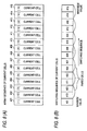
- Fig. 8 is an explanatory diagram for explaining both an arranging structure and a switching sequence of current cells of a current adding type D/A converter according to a fourth embodiment mode of the present invention.
- Fig. 8(A) shows an array sequence of the current cells
- Fig. 1(B) represents a switching sequence of the current cells.
- a current cell 401 through a current cell 415 are made of the same current cells.
- each of these current cells is constituted by employing a constant current source and a switch used to turn ON this constant current source.
- These current cells are arranged in the form of, for example, one column in this order of reference numerals 401 to 415. These reference numerals 401 to 415 correspond to array numbers of the current cells. With respect to output current amounts of these current cells, it is so assumed that characteristics are changed at a constant inclination from the current cell 401 to the current cell 415.
- numerals [1] to [15] denoted on the respective current cells in Fig. 8(A) correspond to switching numbers, namely represent such a sequence that the current cells are switched.
- the current cells defined from the current cell 401 to the current cell 415 are turned ON in the sequential number defined from the switching number [1] to the switching number [15].
- Fig. 8(B) shows current cells which are arranged by rearranging the above-described current cells of Fig. 8(A) in another switching order as shown in Fig. 8(B).
- Reference numerals denoted in the respective current cells show array numbers.
- the current adding type D/A converter of this fourth embodiment mode is featured as follows: That is, when a total number of the current cells is equal to multiple number of "4"-1, the turning-ON sequence of the current cells may cause differences in fluctuations of output current amounts to become constant as to two sets of adjoining current-cell groups, and also may decrease output current characteristic changes in the vicinity of a center point of input data.
- this actual D/A converter when this actual D/A converter is formed by arranging the current cells from the current cell 401 up to the current cell 415, a process fluctuation may occur along a predetermined direction.
- the magnitudes of the output currents of the respective current cells are not always made constant. For example, assuming now that the output current amounts of these current cells are changed by 1 % per one current cell, there are errors of 14 % in the output current amount of the current cell 415 with respect to the current cell 401.
- the switching sequence is determined in such a manner that the current cells having the large fluctuations of the output currents (namely, located on both sides) are turned ON in the order corresponding to such a value nearly equal to either the maximum value or the minimum value, whereas the current cells having the small fluctuations (located in the vicinity of center point) are turned ON in the order of such a value near the center point.
- the characteristics such as the differential linearity errors can be improved because of the following reasons. That is, in the vicinity of the center point of the input data, the distances (namely, array numbers) among the current cells whose ON-sequences are continued are close positions, and the difference in the output current amounts every current cell becomes small.
- the following current cells constitute pair cells from the both ends of the current cell arrangement to the center, namely, both the current cell 401 and the current cell 415 constitute a pair; both the current cell 402 and the current cell 414 constitute a pair; both the current cell 403 and the current cell 413 constitute a pair; both the current cell 404 and the current cell 412 constitute a pair; both the current cell 405 and the current cell 411 constitute a pair; both the current cell 406 and the current cell 410 constitute a pair; and both the current cell 407 and the current cell 409 constitute a pair.
- a summation of last two digits of the array number thereof becomes 16 (namely, current cell number + 1).
- the switching sequence is set in such a manner that the remaining center current cell 408 is turned ON at the center point.
- the divided current cells become odd numbers.
- the current cell 401 and the current cell 415 which own large fluctuations of output current amounts are subdivided.
- One of these paired current cells is firstly turned ON, and the other current cell is finally turned ON.
- Such a switching order is set as follows: That is, a combination between the current cell 402 and the current cell 414 (which are secondly located on both sides), which own the large fluctuation of the output current amounts is turned ON in a second switching order and a third switching order, or in a 13-th switching order and a 14-th switching order among the remaining paired current cells.
- the pairs of the combined current cells are indicated under adjoining states, and the current cells corresponding thereto are turned ON in the order of the switching numbers from the minimum value to the maximum value.
- the current cell 401 is firstly turned ON.
- the pair of both the current cell 413 and the current cell 403 are turned ON in a second switching order and a third switching order.
- the pair of both the current cell 402 and the current cell 414 are turned ON in a 13-th switching order and a 14-th switching order.
- the current cell 411, the current cell 405, the current cell 409, the current cell 407, the current cell 408, the current cell 406, the current cell 410, the current cell 404, the current cell 412, the current cell 402, and the current cell 414 are sequentially turned ON.
- the current cell 415 is turned ON, so that all of the current cells are turned ON.
- the summation of the current amounts flowing from a plurality of current cells 401 to 415 is controlled.
- This current is converted into a voltage by the output resistor 5, so that the D/A converting operation as to the input data is carried out.
- the analog output signal can be obtained with respect to the digital input data.
- the plural current cells are sequentially turned ON from the current cell 401 to the current cell 415 at last in response to the values of the input data from the minimum value to the maximum value.
- the plural currents may be turned ON from the current cell 415 up to the current cell 401.
- the switching sequence operations at the respective pairs of the adjoining current cells are reversed in an opposite sense, namely, the pair of the current cell 413 and the current cell 403, the pair of the current cell 411 and the current cell 405, ---, and the like. Even when the switching sequence is set in this order, a similar effect to that of the case shown in Fig. 1 is obtained.
- a similar effect may be obtained even in such a case that the total number of current cells is divided by a power of 2 (in this case, either 1/2 subdivision or 1/4 subdivision except for central current cell) while setting the center point of the switching sequence as the boundary, and switching sequences as to two sets of the current cell groups which are located at the symmetrical positions as to this center point are replaced.
- the current cells when the current cells are combined as the pairs, a total number of these paired current cells becomes the odd numbers while setting a center point as a boundary, and therefore, the current cells located at both ends become extra current cells.
- This current cell 401 is turned ON at a minimum value, whereas the current cell 415 is turned ON at a maximum value.
- both the differential linearity errors and the non-linear errors in the vicinity of the center point can be reduced.
- the output current characteristics which sandwich the center point can be made symmetrical.
- the errors caused by the fluctuations in the output current amounts in the usually-operated frequency rage of the D/A converter can be decreased, and the converting precision can be increased so as to improve the characteristic, so that the more suitable output signal can be acquired.
- the characteristic of the D/A converter for the analog output signal can be made symmetrical with respect to positive/negative characteristics. In particular, both the noise and the distortion occurred in the vicinity of the center point can be reduced.
- the precision thereof in the current adding type D/A converter, the precision thereof can be improved in the vicinity of the center point of the input signal range, and also the distortions of the corresponding output signals can be reduced.
- the precision of this D/A converter required when an output signal owns a small amplitude may become more important than that required when an output signal owns a large amplitude.
- the precision of the D/A converters itself is identical to each other, generally speaking, the characteristic obtained when the output signal owns the small amplitude corresponding to the normally-used range can be improved.
Landscapes
- Engineering & Computer Science (AREA)
- Theoretical Computer Science (AREA)
- Analogue/Digital Conversion (AREA)
Applications Claiming Priority (2)
| Application Number | Priority Date | Filing Date | Title |
|---|---|---|---|
| JP2000194624A JP3528958B2 (ja) | 2000-06-28 | 2000-06-28 | 電流加算型da変換器 |
| JP2000194624 | 2000-06-28 |
Publications (3)
| Publication Number | Publication Date |
|---|---|
| EP1168628A2 EP1168628A2 (en) | 2002-01-02 |
| EP1168628A3 EP1168628A3 (en) | 2004-01-28 |
| EP1168628B1 true EP1168628B1 (en) | 2006-08-16 |
Family
ID=18693418
Family Applications (1)
| Application Number | Title | Priority Date | Filing Date |
|---|---|---|---|
| EP01115464A Expired - Lifetime EP1168628B1 (en) | 2000-06-28 | 2001-06-27 | Current adding type D/A converter |
Country Status (4)
| Country | Link |
|---|---|
| US (1) | US6452527B2 (ja) |
| EP (1) | EP1168628B1 (ja) |
| JP (1) | JP3528958B2 (ja) |
| DE (1) | DE60122248T2 (ja) |
Families Citing this family (12)
| Publication number | Priority date | Publication date | Assignee | Title |
|---|---|---|---|---|
| KR100730398B1 (ko) * | 2002-05-27 | 2007-06-20 | 노키아 코포레이션 | D/a 변환기 교정 방법 및 d/a 변환기 |
| JP2004208060A (ja) * | 2002-12-25 | 2004-07-22 | Renesas Technology Corp | D/aコンバータ |
| US6720898B1 (en) * | 2003-04-10 | 2004-04-13 | Maxim Integrated Products, Inc. | Current source array for high speed, high resolution current steering DACs |
| JP2007521732A (ja) * | 2003-06-27 | 2007-08-02 | コーニンクレッカ フィリップス エレクトロニクス エヌ ヴィ | 低減された動的非線形性を有する電流操作d/a変換器 |
| US7173552B1 (en) | 2003-10-01 | 2007-02-06 | Analog Devices, Inc. | High accuracy segmented DAC |
| JP4757006B2 (ja) * | 2005-12-07 | 2011-08-24 | ルネサスエレクトロニクス株式会社 | 電流源セル配置構造およびda変換器 |
| JP2007227990A (ja) * | 2006-02-21 | 2007-09-06 | Oki Electric Ind Co Ltd | タイミング生成回路及びそれを用いたデジタル/アナログ変換器 |
| EP2746891B1 (en) * | 2012-12-20 | 2015-06-03 | Imec | A current waveform generator |
| US10038452B2 (en) * | 2016-09-23 | 2018-07-31 | Analog Devices, Inc. | Incremental preloading in an analog-to-digital converter |
| US9712181B1 (en) * | 2016-09-23 | 2017-07-18 | Analog Devices, Inc. | Incremental preloading in an analog-to-digital converter |
| US10892767B1 (en) * | 2019-09-20 | 2021-01-12 | Nxp Usa, Inc. | High accuracy matching system and method therefor |
| TWI768973B (zh) * | 2021-06-17 | 2022-06-21 | 瑞昱半導體股份有限公司 | 校正輸出電流的方法、電流控制系統及電壓控制系統 |
Family Cites Families (8)
| Publication number | Priority date | Publication date | Assignee | Title |
|---|---|---|---|---|
| US3995304A (en) * | 1972-01-10 | 1976-11-30 | Teledyne, Inc. | D/A bit switch |
| JPS61240716A (ja) * | 1985-04-17 | 1986-10-27 | Mitsubishi Electric Corp | ディジタルアナログコンバ−タ |
| US4864215A (en) * | 1988-02-16 | 1989-09-05 | U.S. Philips Corp. | Current source arrangement |
| JPH02253719A (ja) | 1989-03-27 | 1990-10-12 | Matsushita Electric Ind Co Ltd | ディジタル・アナログ変換器 |
| JPH05191289A (ja) | 1992-01-14 | 1993-07-30 | Sony Corp | 電流加算方式d/aコンバータ |
| JPH05259916A (ja) | 1992-03-11 | 1993-10-08 | Matsushita Electric Ind Co Ltd | 電流加算型d/a変換器 |
| US5949362A (en) * | 1997-08-22 | 1999-09-07 | Harris Corporation | Digital-to-analog converter including current cell matrix with enhanced linearity and associated methods |
| JP2000188550A (ja) | 1998-12-22 | 2000-07-04 | Motorola Japan Ltd | デジタル・アナログ変換回路 |
-
2000
- 2000-06-28 JP JP2000194624A patent/JP3528958B2/ja not_active Expired - Fee Related
-
2001
- 2001-06-27 DE DE60122248T patent/DE60122248T2/de not_active Expired - Lifetime
- 2001-06-27 EP EP01115464A patent/EP1168628B1/en not_active Expired - Lifetime
- 2001-06-27 US US09/893,278 patent/US6452527B2/en not_active Expired - Fee Related
Also Published As
| Publication number | Publication date |
|---|---|
| US20020008652A1 (en) | 2002-01-24 |
| EP1168628A2 (en) | 2002-01-02 |
| US6452527B2 (en) | 2002-09-17 |
| JP2002016498A (ja) | 2002-01-18 |
| DE60122248D1 (de) | 2006-09-28 |
| DE60122248T2 (de) | 2006-12-07 |
| JP3528958B2 (ja) | 2004-05-24 |
| EP1168628A3 (en) | 2004-01-28 |
Similar Documents
| Publication | Publication Date | Title |
|---|---|---|
| US5243347A (en) | Monotonic current/resistor digital-to-analog converter and method of operation | |
| EP1168628B1 (en) | Current adding type D/A converter | |
| US5495245A (en) | Digital-to-analog converter with segmented resistor string | |
| KR100436357B1 (ko) | 다중출력단을갖는디지털아날로그변환기및그변환방법 | |
| US4503421A (en) | Digital to analog converter | |
| US5059978A (en) | Resistor-string digital to analog converters with auxiliary coarse ladders | |
| EP0259566B1 (en) | Networks used in A/D and D/A converters with correction for differential errors | |
| US4868571A (en) | Digital to analog converter | |
| US8941522B2 (en) | Segmented digital-to-analog converter having weighted current sources | |
| US6617989B2 (en) | Resistor string DAC with current source LSBs | |
| CN1484889A (zh) | 数模转换器 | |
| GB2069265A (en) | D/a converters | |
| GB2344479A (en) | Resistor-type D/A convertor having a highly linear transconductor | |
| US6509857B1 (en) | Digital-to-analog converting method and digital-to-analog converter | |
| CN111434041A (zh) | 内插数/模转换器(dac) | |
| JPS61240716A (ja) | ディジタルアナログコンバ−タ | |
| KR100311043B1 (ko) | 고속 스위칭 가능하고 정밀하게 전압 변환 가능한 디지털 아날로그 변환기 | |
| US20020008650A1 (en) | Digital-analogue transformer | |
| JPH04162830A (ja) | D/aコンバータ | |
| US6642867B1 (en) | Replica compensated heterogeneous DACs and methods | |
| US4580131A (en) | Binarily weighted D to a converter ladder with inherently reduced ladder switching noise | |
| US4591826A (en) | Gray code DAC ladder | |
| EP0135274A2 (en) | Digital-to-analog converter | |
| JP2001127634A (ja) | ディジタル・アナログ変換器 | |
| JPH0712150B2 (ja) | ディジタル・アナログ変換器 |
Legal Events
| Date | Code | Title | Description |
|---|---|---|---|
| PUAI | Public reference made under article 153(3) epc to a published international application that has entered the european phase |
Free format text: ORIGINAL CODE: 0009012 |
|
| AK | Designated contracting states |
Kind code of ref document: A2 Designated state(s): AT BE CH CY DE DK ES FI FR GB GR IE IT LI LU MC NL PT SE TR |
|
| AX | Request for extension of the european patent |
Free format text: AL;LT;LV;MK;RO;SI |
|
| PUAL | Search report despatched |
Free format text: ORIGINAL CODE: 0009013 |
|
| AK | Designated contracting states |
Kind code of ref document: A3 Designated state(s): AT BE CH CY DE DK ES FI FR GB GR IE IT LI LU MC NL PT SE TR |
|
| AX | Request for extension of the european patent |
Extension state: AL LT LV MK RO SI |
|
| 17P | Request for examination filed |
Effective date: 20040414 |
|
| 17Q | First examination report despatched |
Effective date: 20040511 |
|
| AKX | Designation fees paid |
Designated state(s): DE FR GB |
|
| GRAP | Despatch of communication of intention to grant a patent |
Free format text: ORIGINAL CODE: EPIDOSNIGR1 |
|
| RAP1 | Party data changed (applicant data changed or rights of an application transferred) |
Owner name: MATSUSHITA ELECTRIC INDUSTRIAL CO., LTD. |
|
| GRAS | Grant fee paid |
Free format text: ORIGINAL CODE: EPIDOSNIGR3 |
|
| GRAA | (expected) grant |
Free format text: ORIGINAL CODE: 0009210 |
|
| AK | Designated contracting states |
Kind code of ref document: B1 Designated state(s): DE FR GB |
|
| REG | Reference to a national code |
Ref country code: GB Ref legal event code: FG4D |
|
| REF | Corresponds to: |
Ref document number: 60122248 Country of ref document: DE Date of ref document: 20060928 Kind code of ref document: P |
|
| ET | Fr: translation filed | ||
| PLBE | No opposition filed within time limit |
Free format text: ORIGINAL CODE: 0009261 |
|
| STAA | Information on the status of an ep patent application or granted ep patent |
Free format text: STATUS: NO OPPOSITION FILED WITHIN TIME LIMIT |
|
| 26N | No opposition filed |
Effective date: 20070518 |
|
| PGFP | Annual fee paid to national office [announced via postgrant information from national office to epo] |
Ref country code: FR Payment date: 20100709 Year of fee payment: 10 |
|
| PGFP | Annual fee paid to national office [announced via postgrant information from national office to epo] |
Ref country code: DE Payment date: 20100625 Year of fee payment: 10 Ref country code: GB Payment date: 20100623 Year of fee payment: 10 |
|
| GBPC | Gb: european patent ceased through non-payment of renewal fee |
Effective date: 20110627 |
|
| REG | Reference to a national code |
Ref country code: FR Ref legal event code: ST Effective date: 20120229 |
|
| REG | Reference to a national code |
Ref country code: DE Ref legal event code: R119 Ref document number: 60122248 Country of ref document: DE Effective date: 20120103 |
|
| PG25 | Lapsed in a contracting state [announced via postgrant information from national office to epo] |
Ref country code: FR Free format text: LAPSE BECAUSE OF NON-PAYMENT OF DUE FEES Effective date: 20110630 Ref country code: DE Free format text: LAPSE BECAUSE OF NON-PAYMENT OF DUE FEES Effective date: 20120103 |
|
| PG25 | Lapsed in a contracting state [announced via postgrant information from national office to epo] |
Ref country code: GB Free format text: LAPSE BECAUSE OF NON-PAYMENT OF DUE FEES Effective date: 20110627 |