EP1168441A2 - Mehrlagenleitersubstrat und Halbleiterbauteil damit - Google Patents
Mehrlagenleitersubstrat und Halbleiterbauteil damit Download PDFInfo
- Publication number
- EP1168441A2 EP1168441A2 EP01113671A EP01113671A EP1168441A2 EP 1168441 A2 EP1168441 A2 EP 1168441A2 EP 01113671 A EP01113671 A EP 01113671A EP 01113671 A EP01113671 A EP 01113671A EP 1168441 A2 EP1168441 A2 EP 1168441A2
- Authority
- EP
- European Patent Office
- Prior art keywords
- wiring
- layer
- insulating layer
- substrates
- wiring substrate
- Prior art date
- Legal status (The legal status is an assumption and is not a legal conclusion. Google has not performed a legal analysis and makes no representation as to the accuracy of the status listed.)
- Withdrawn
Links
Images




Classifications
-
- H—ELECTRICITY
- H05—ELECTRIC TECHNIQUES NOT OTHERWISE PROVIDED FOR
- H05K—PRINTED CIRCUITS; CASINGS OR CONSTRUCTIONAL DETAILS OF ELECTRIC APPARATUS; MANUFACTURE OF ASSEMBLAGES OF ELECTRICAL COMPONENTS
- H05K3/00—Apparatus or processes for manufacturing printed circuits
- H05K3/46—Manufacturing multilayer circuits
-
- H—ELECTRICITY
- H05—ELECTRIC TECHNIQUES NOT OTHERWISE PROVIDED FOR
- H05K—PRINTED CIRCUITS; CASINGS OR CONSTRUCTIONAL DETAILS OF ELECTRIC APPARATUS; MANUFACTURE OF ASSEMBLAGES OF ELECTRICAL COMPONENTS
- H05K3/00—Apparatus or processes for manufacturing printed circuits
- H05K3/36—Assembling printed circuits with other printed circuits
- H05K3/361—Assembling flexible printed circuits with other printed circuits
- H05K3/363—Assembling flexible printed circuits with other printed circuits by soldering
-
- H—ELECTRICITY
- H10—SEMICONDUCTOR DEVICES; ELECTRIC SOLID-STATE DEVICES NOT OTHERWISE PROVIDED FOR
- H10W—GENERIC PACKAGES, INTERCONNECTIONS, CONNECTORS OR OTHER CONSTRUCTIONAL DETAILS OF DEVICES COVERED BY CLASS H10
- H10W70/00—Package substrates; Interposers; Redistribution layers [RDL]
- H10W70/60—Insulating or insulated package substrates; Interposers; Redistribution layers
- H10W70/62—Insulating or insulated package substrates; Interposers; Redistribution layers characterised by their interconnections
- H10W70/65—Shapes or dispositions of interconnections
- H10W70/657—Shapes or dispositions of interconnections on sidewalls or bottom surfaces of the package substrates, interposers or redistribution layers
-
- H—ELECTRICITY
- H10—SEMICONDUCTOR DEVICES; ELECTRIC SOLID-STATE DEVICES NOT OTHERWISE PROVIDED FOR
- H10W—GENERIC PACKAGES, INTERCONNECTIONS, CONNECTORS OR OTHER CONSTRUCTIONAL DETAILS OF DEVICES COVERED BY CLASS H10
- H10W70/00—Package substrates; Interposers; Redistribution layers [RDL]
- H10W70/60—Insulating or insulated package substrates; Interposers; Redistribution layers
- H10W70/67—Insulating or insulated package substrates; Interposers; Redistribution layers characterised by their insulating layers or insulating parts
- H10W70/688—Flexible insulating substrates
-
- H—ELECTRICITY
- H10—SEMICONDUCTOR DEVICES; ELECTRIC SOLID-STATE DEVICES NOT OTHERWISE PROVIDED FOR
- H10W—GENERIC PACKAGES, INTERCONNECTIONS, CONNECTORS OR OTHER CONSTRUCTIONAL DETAILS OF DEVICES COVERED BY CLASS H10
- H10W90/00—Package configurations
-
- H—ELECTRICITY
- H05—ELECTRIC TECHNIQUES NOT OTHERWISE PROVIDED FOR
- H05K—PRINTED CIRCUITS; CASINGS OR CONSTRUCTIONAL DETAILS OF ELECTRIC APPARATUS; MANUFACTURE OF ASSEMBLAGES OF ELECTRICAL COMPONENTS
- H05K1/00—Printed circuits
- H05K1/02—Details
- H05K1/14—Structural association of two or more printed circuits
- H05K1/144—Stacked arrangements of planar printed circuit boards
-
- H—ELECTRICITY
- H05—ELECTRIC TECHNIQUES NOT OTHERWISE PROVIDED FOR
- H05K—PRINTED CIRCUITS; CASINGS OR CONSTRUCTIONAL DETAILS OF ELECTRIC APPARATUS; MANUFACTURE OF ASSEMBLAGES OF ELECTRICAL COMPONENTS
- H05K2201/00—Indexing scheme relating to printed circuits covered by H05K1/00
- H05K2201/03—Conductive materials
- H05K2201/0332—Structure of the conductor
- H05K2201/0388—Other aspects of conductors
- H05K2201/0397—Tab
-
- H—ELECTRICITY
- H05—ELECTRIC TECHNIQUES NOT OTHERWISE PROVIDED FOR
- H05K—PRINTED CIRCUITS; CASINGS OR CONSTRUCTIONAL DETAILS OF ELECTRIC APPARATUS; MANUFACTURE OF ASSEMBLAGES OF ELECTRICAL COMPONENTS
- H05K2201/00—Indexing scheme relating to printed circuits covered by H05K1/00
- H05K2201/10—Details of components or other objects attached to or integrated in a printed circuit board
- H05K2201/10613—Details of electrical connections of non-printed components, e.g. special leads
- H05K2201/10621—Components characterised by their electrical contacts
- H05K2201/10681—Tape Carrier Package [TCP]; Flexible sheet connector
-
- H—ELECTRICITY
- H10—SEMICONDUCTOR DEVICES; ELECTRIC SOLID-STATE DEVICES NOT OTHERWISE PROVIDED FOR
- H10W—GENERIC PACKAGES, INTERCONNECTIONS, CONNECTORS OR OTHER CONSTRUCTIONAL DETAILS OF DEVICES COVERED BY CLASS H10
- H10W70/00—Package substrates; Interposers; Redistribution layers [RDL]
- H10W70/60—Insulating or insulated package substrates; Interposers; Redistribution layers
-
- H—ELECTRICITY
- H10—SEMICONDUCTOR DEVICES; ELECTRIC SOLID-STATE DEVICES NOT OTHERWISE PROVIDED FOR
- H10W—GENERIC PACKAGES, INTERCONNECTIONS, CONNECTORS OR OTHER CONSTRUCTIONAL DETAILS OF DEVICES COVERED BY CLASS H10
- H10W72/00—Interconnections or connectors in packages
- H10W72/834—Interconnections on sidewalls of chips
-
- H—ELECTRICITY
- H10—SEMICONDUCTOR DEVICES; ELECTRIC SOLID-STATE DEVICES NOT OTHERWISE PROVIDED FOR
- H10W—GENERIC PACKAGES, INTERCONNECTIONS, CONNECTORS OR OTHER CONSTRUCTIONAL DETAILS OF DEVICES COVERED BY CLASS H10
- H10W90/00—Package configurations
- H10W90/20—Configurations of stacked chips
- H10W90/297—Configurations of stacked chips characterised by the through-semiconductor vias [TSVs] in the stacked chips
-
- H—ELECTRICITY
- H10—SEMICONDUCTOR DEVICES; ELECTRIC SOLID-STATE DEVICES NOT OTHERWISE PROVIDED FOR
- H10W—GENERIC PACKAGES, INTERCONNECTIONS, CONNECTORS OR OTHER CONSTRUCTIONAL DETAILS OF DEVICES COVERED BY CLASS H10
- H10W90/00—Package configurations
- H10W90/701—Package configurations characterised by the relative positions of pads or connectors relative to package parts
- H10W90/721—Package configurations characterised by the relative positions of pads or connectors relative to package parts of bump connectors
-
- H—ELECTRICITY
- H10—SEMICONDUCTOR DEVICES; ELECTRIC SOLID-STATE DEVICES NOT OTHERWISE PROVIDED FOR
- H10W—GENERIC PACKAGES, INTERCONNECTIONS, CONNECTORS OR OTHER CONSTRUCTIONAL DETAILS OF DEVICES COVERED BY CLASS H10
- H10W90/00—Package configurations
- H10W90/701—Package configurations characterised by the relative positions of pads or connectors relative to package parts
- H10W90/721—Package configurations characterised by the relative positions of pads or connectors relative to package parts of bump connectors
- H10W90/722—Package configurations characterised by the relative positions of pads or connectors relative to package parts of bump connectors between stacked chips
-
- H—ELECTRICITY
- H10—SEMICONDUCTOR DEVICES; ELECTRIC SOLID-STATE DEVICES NOT OTHERWISE PROVIDED FOR
- H10W—GENERIC PACKAGES, INTERCONNECTIONS, CONNECTORS OR OTHER CONSTRUCTIONAL DETAILS OF DEVICES COVERED BY CLASS H10
- H10W90/00—Package configurations
- H10W90/701—Package configurations characterised by the relative positions of pads or connectors relative to package parts
- H10W90/721—Package configurations characterised by the relative positions of pads or connectors relative to package parts of bump connectors
- H10W90/724—Package configurations characterised by the relative positions of pads or connectors relative to package parts of bump connectors between a chip and a stacked insulating package substrate, interposer or RDL
Definitions
- the present invention relates to a multi-layered wiring substrate and a semiconductor device using a multi-layered wiring substrate.
- conductive layers such as copper foils are formed on opposite surfaces of an insulating substrate (insulating layer) 10 in the form of a sheet or plate and made of a resin material such as polyimide.
- the conductive layers of the insulating substrate 10 are etched so that a wiring substrate 14 comprised of the insulating substrate 10 and predetermined circuit patterns (wiring layers) 12 formed on opposite surfaces thereof can be obtained, as shown in Fig. 11(a).
- through holes 16 which extend through the insulating substrate 10 and the wiring layers 12, are formed at portions at which the wiring'layers 12 of the wiring substrates 14 to be superimposed are to be electrically connected, as shown in Fig. 11(b).
- the inner peripheral surfaces of the through holes 16 and the surface portions of the wiring layers 12 corresponding to the through holes 16 are coated with, for example, copper plating 18, so that connecting portions (so-called "vias") 18 for establishing electrical connection between the wiring layers 12 on the opposite surfaces of the insulating substrate 10 are formed, as shown in Fig. 11(c). Note that upon plating the inner peripheral surface of the through holes 16, electroless plating is first conducted, and thereafter, electroplating is conducted.
- a plurality of wiring substrates 14 are superimposed through an adhesive 21.
- the connecting portions 18 of the insulating substrates 10 are aligned along lines in the direction of the superimposition, and a heated reflowable alloy (first conductor) 22, such as a solder is introduced in the aligned connecting portions 18 to connect the same, as shown in Fig. 11(d). Consequently, a multi-layered wiring substrate 23 in which the wiring layers 12 of the wiring substrates 14 are electrically connected is obtained.
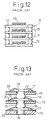
- Figs. 12 and 13 show a known multi-layered semiconductor device in which electrical connection between the layers is established by solder balls.
- Fig. 12 shows a side sectional view of the whole structure of the semiconductor device and
- Fig. 13 shows an enlarged view of the part "A" in Fig. 12.
- a circuit pattern (wiring layer) 12 of copper is formed on one surface of an insulating substrate 10 made of a resin material, such as polyimide and a semiconductor chip 40 is formed thereon.
- the semiconductor packages are multi-layered to form a multi-layered semiconductor device.
- the insulating substrates 10 are provided with through holes 16 extending therethrough and wiring layers 12 which are formed and exposed on one surface of each insulating substrate.
- numeral 20 designates the adhesive to secure the insulating substrates (polyimide) 10 and the wiring layers (e.g., copper) 12, and numeral 17 designates the solder resist.
- a multi-layered wiring substrate according to the present invention in which wiring layers and insulating layers are alternately superimposed, and at least a pair of insulating layers formed on front and rear surfaces of the insulating layers are electrically connected by connecting portions extending through the insulating layers is characterized in that the wiring layers and the insulating layers are formed by superimposing wiring substrates, each being made of a plate or sheet provided on only one of the surfaces of the insulating layer with a wiring layer, in such a way that the wiring layers and the insulating layers are alternately arranged, wherein the connecting portions are provided with extensions formed by a part of the wiring layers extending into the area of opening portions which extend through the insulating layers of the wiring substrates, so that the extensions and the wiring layers of the adjacent wiring substrate, located adjacent the insulating layer thereof, are electrically connected through low melting metal portions.
- the portions can be through holes formed in the insulating layers.
- the holes may be cut-away portions formed at the peripheries of the insulating layers.
- the low melting metal portions can be solder balls or solder pastes, or materials derived therefrom.
- a semiconductor device can be comprised of a multi-layered wiring substrate which is provided with the wiring substrates which are in turn provided on the insulating layers thereof with recesses in which the semiconductor elements are received, and the wiring layers which define, at their one end, lead portions electrically connected to electrode terminals of the semiconductor elements and, at the other ends, extensions extending in the opening portions, and semiconductor elements which are arranged in the recesses so that the surfaces thereof on which the electrode terminals are formed are oriented toward the wiring layers, so that the lead portions of the wiring layers are electrically connected to the electrode terminals.
- Figs. 1 and 2 show a single layer of a wiring substrate 26 for producing a multi-layered wiring substrate according to this invention.
- Fig. 1 shows a sectional view and Fig. 2 shows a top view thereof.
- the wiring substrate 26 is comprised of an insulating substrate 10 as an insulating layer in the form of a sheet or plate made of a resin material, such as polyimide, and a wiring layer 12 made of, for example copper, formed on only one surface (upper surface in Fig. 1) of the insulating substrate 10.
- Numeral 20 designates the adhesive which adheres the insulating substrate (e.g., polyimide) 10 and the wiring layer (e.g., copper) 12.
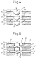
- the insulating substrates 10 and the wiring layers 12 are alternately arranged, as shown in Fig. 5.
- the wiring substrate 26 is provided with a connecting portion 28 for electrically interconnecting the wiring layers 12 of the adjacent wiring substrates 26.
- the connecting portion 28 is provided with an extension portion 30 of the wiring layer 12 formed on the upper surface of the insulating substrate 10 and protruding into an opening 16 (through hole in the embodiment illustrated in Fig. 1) formed to connect the front and rear surfaces of the insulating substrate 10.
- the extension 30 which is a part of the wiring layer 12 and extends into the area of the through hole 16 lies over the major part of the area of the through hole 16.
- the extension 30 of the wiring layer 12 in the area of the through hole 16 is not bent inwardly and is flush with the portion of the wiring layer 12 that is located on the upper surface of the insulating substrate 10.
- the wiring substrate 26 constructed as above can be manufactured by a known process. For instance, an insulating substrate 10, as an insulating layer, provided on its one surface with an integral conductor layer such as a copper foil is prepared. The conductor layer is etched by photolithography to obtain a wiring substrate 26 having a predetermined pattern of the wiring layer 12. It is possible to form a through hole 16 in the insulating substrate 10 by drilling, prior to the formation of the wiring layer 12 on one of the surfaces of the insulating substrate 10. Alternatively, it is possible to form the through hole 16 by a laser, etc., after the wiring layer 12 is formed on one of the surfaces of the insulating substrate 10.
- the through hole 16 has a circular cross section in the embodiment illustrated in Figs. 1 and 2, the shape is not limited, as a matter of fact, to a circle and can be a rectangular shape, a polygonal shape or any shape.
- a solder ball as a low melting metal is fed into the through hole 16 of the insulating substrate 10 and is mounted to the extension 30 of the wiring layer 12.
- a solder portion 32 is formed on the extension 30 so as not to come away therefrom, by reflowing of the solder ball, as can be seen in Fig. 3.
- Fig. 4 shows a plurality of superimposed wiring substrates 26 having the solder portions 32 formed thereon, as shown in Fig. 3.
- the wiring substrates 26 are superimposed so that the through holes 16 thereof, which constitute the connecting portions, are aligned. In this state, the reflowing of the solder portions 32 is carried out to melt the same. Consequently, the wiring layers 12 of the adjacent wiring substrates 26 are connected to establish electrical connection therebetween, as can be seen in Fig. 5.
- the wiring layers 12 of the wiring substrates 26 which constitute three layers, i.e., the upper layer, the intermediate layer and the lower layer are electrically connected at the same position, in the arrangement shown in Figs. 4 and 5, it is not always necessary to connect the three layers at the same position in the present invention. Namely, in the basic concept of the present invention, the wiring layers of at least two layers are electrically connected.
- solder portions 32 derived from the solder balls are used as a low melting metal in the embodiment illustrated in Figs. 1 through 5, it is alternatively possible to use solder paste.
- the solder paste is supplied to the through hole 16 in place of the solder portion 32 derived from the solder ball in Fig. 3 and is connected to the extension of the wiring layer 12. After superimposition of the wiring substrates, the reflowing of the solder paste causes the wiring layers 12 of the adjacent wiring substrates 26 to be interconnected through the fused solder to thereby establish an electrical connection therebetween.
- the solder ball is more preferable than the solder paste, from the viewpoint of provision of the necessary amount of solder for the connection between the layers.
- the connecting portions 28 of the wiring layers 12 of the wiring substrates 26 are constituted by the through holes 16 formed in the insulating substrates 10.
- cut-away portions 36 are formed at the outer peripheral edges (peripheral edges) of the wiring substrates 26.
- the cut-away portions 36 whose shape in plan view is, for example, semicircular, are formed, in place of the through holes 16, at the outer peripheral edge portions of the wiring substrates 26.
- a part of the wiring layer 12 formed on one surface of each insulating substrate 10 extends into the cut-away portion 36 to define the extension 30.
- the solder ball is supplied to the cut-away portion 36 of each wiring substrate 26 to form the solder portion 32 on the extension 30 of the wiring layer 12.
- the wiring substrates 26 provided with the cut-away portions 36 and the extensions 30 are superimposed so that the inner peripheral surfaces of the cut-away portions 36 are connected.
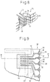
- solder portions 32 causes the extensions 30 of the wiring substrates 26 to be electrically connected so as to form the connecting portions 28, as shown in Figs. 7 and 8. Consequently, the multi-layered wiring substrate 24, in which the wiring layers 12 are electrically connected between the layers, can be obtained.
- a multi-layered wiring substrate comprised of wiring substrates (e.g., substrates having copper foil tapes on one surface thereof) which are provided, on only one surface of the insulating layers, with conductive layers and which are less expensive than a conventional wiring substrate provided on its opposite surfaces with conductive layers, can be produced.
- the connecting portions 28 which connect the adjacent wiring layers 12 opposed to each other through the insulating substrate (insulating layer) 10 can be formed without using electroless plating, the manufacturing cost can be remarkably reduced, and thus the component cost can be reduced.
- the connecting portions 28 are made of the cut-away portions 36 formed at the outer peripheral edge of the wiring substrate 26, and the solder portions 32 are formed on the extensions 30 of the wiring layers 12 which extend into the cut-away portions 36 and are subjected to reflowing upon superimposition.
- the connecting portions 28 may be made of the through holes formed in the wiring substrates 26, in place of the cut-away portions formed at the peripheral edges of the wiring substrates 26.
- the semiconductor device 38 is made of the multi-layered wiring substrate 24 composed of the wiring substrates 26 which are each provided with the insulating substrate 10 and the wiring layer 12 formed on only one of the surfaces of the insulating substrate 10 and which are superimposed so that the wiring layers 12 and the insulating substrates 10 are alternately arranged.
- each wiring substrate 24 is provided with a receiving recess (device hole) 42 in which the semiconductor element 40 is received.
- the plane wiring layer 12 is exposed to the bottom surface (upper surface in Fig. 10) of each receiving recess 42 and the lead portion in the area of the receiving recess 42 defines a window 44 extending through each wiring substrate 26 since the portion of the conductive layer other than the lead portion is etched and removed.
- Each wiring layer 12 defines a lead portion 48 whose one end (left end in Fig. 9 or 10) extends in the receiving recess 42 and is connected to the electrode terminal 46 of the semiconductor element 40.
- the other end (right end in Fig. 9 or 10) of the lead portion 48 extends in the area of the cut-away portion 36 formed at the outer peripheral edge of the insulating substrate 10 to define the extension 30.
- the semiconductor element 40 is received in each receiving recess 42 of each wiring substrate 26, so that the surface 40a (electrode terminal forming surface) of the semiconductor element on which the electrode terminal 46 is formed is opposed to the wiring layer 12.
- the lead portion 48 of the wiring layer 12 is connected to the electrode terminal 46 exposed to the electrode terminal forming surface 40a.
- the semiconductor elements 40 are mounted in the receiving recesses 42, the latter are filled with a resin material 50 to seal the side surfaces of the semiconductor elements 40, the electrode terminal forming surfaces 40a and the lead portions 48 of the wiring layers 12.
- the wiring substrates 26 are superimposed so that the corresponding cut-away portions 36 communicate with each other and the extensions 30 extending in the areas of the communicating cut-away portions 36 of the wiring substrates 26 are electrically connected through the solder portions 32 to obtain the semiconductor device 38.
- numeral 54 designates the adhesion layer by which the semiconductor element 40 is adhered to the wiring layer 12 and numeral 20 designates the adhesion layer by which the wiring layer 12 is adhered to the insulating substrate 10.
- each of the superimposed wiring substrates 26 is provided with the receiving recess 42 in which the semiconductor element 40 is mounted, and hence it can be considered that a plurality of sub-semiconductor devices 52 are superimposed to form a semiconductor apparatus 38. Moreover, it can be considered that each wiring substrate 26 provided with the receiving recess 42 constitutes a sub-semiconductor device 52 which in turn constitutes a single semiconductor package.
- a multi-layered wiring substrate comprised of wiring substrates (e.g., substrates having copper foil tapes on one surface thereof) which are provided, on only one surface of the insulating layers, with conductive layers and which are less expensive than a conventional wiring substrate provided on its opposite surfaces with conductive layers, can be produced.
- the connecting portions which are formed by, for example, etching the conductive layer and which connect the wiring layers of the adjacent layers can be formed without using electroless plating, the manufacturing cost can be remarkably reduced, and thus the component cost can be reduced and the thickness of the device can be reduced.
- the layers be electrically connected without a special machining operation, such as partial bending of the wiring layers, but also the extensions of the wiring layers can be connected through a low melting metal, such as a solder, thus resulting in a reduction in the manufacturing cost.
- a low melting metal such as a solder
Landscapes
- Engineering & Computer Science (AREA)
- Manufacturing & Machinery (AREA)
- Microelectronics & Electronic Packaging (AREA)
- Production Of Multi-Layered Print Wiring Board (AREA)
- Internal Circuitry In Semiconductor Integrated Circuit Devices (AREA)
Applications Claiming Priority (2)
| Application Number | Priority Date | Filing Date | Title |
|---|---|---|---|
| JP2000194938A JP2002009192A (ja) | 2000-06-23 | 2000-06-23 | 多層配線基板及び半導体装置 |
| JP2000194938 | 2000-06-23 |
Publications (2)
| Publication Number | Publication Date |
|---|---|
| EP1168441A2 true EP1168441A2 (de) | 2002-01-02 |
| EP1168441A3 EP1168441A3 (de) | 2005-06-15 |
Family
ID=18693689
Family Applications (1)
| Application Number | Title | Priority Date | Filing Date |
|---|---|---|---|
| EP01113671A Withdrawn EP1168441A3 (de) | 2000-06-23 | 2001-06-19 | Mehrlagenleitersubstrat und Halbleiterbauteil damit |
Country Status (4)
| Country | Link |
|---|---|
| US (1) | US6518672B2 (de) |
| EP (1) | EP1168441A3 (de) |
| JP (1) | JP2002009192A (de) |
| KR (1) | KR100821596B1 (de) |
Cited By (1)
| Publication number | Priority date | Publication date | Assignee | Title |
|---|---|---|---|---|
| WO2017108121A1 (en) * | 2015-12-23 | 2017-06-29 | Intel IP Corporation | Semiconductor die package with more than one hanging die |
Families Citing this family (1)
| Publication number | Priority date | Publication date | Assignee | Title |
|---|---|---|---|---|
| KR100747393B1 (ko) * | 2003-04-25 | 2007-08-07 | 미쓰이 긴조꾸 고교 가부시키가이샤 | 전자 부품 실장용 필름 캐리어 테이프와 그 제조 방법 및솔더 레지스트 도포용 스크린 |
Family Cites Families (7)
| Publication number | Priority date | Publication date | Assignee | Title |
|---|---|---|---|---|
| US4956694A (en) * | 1988-11-04 | 1990-09-11 | Dense-Pac Microsystems, Inc. | Integrated circuit chip stacking |
| JP3126784B2 (ja) * | 1992-01-27 | 2001-01-22 | 株式会社日立製作所 | 積層マルチチップ半導体装置 |
| US5832600A (en) * | 1995-06-06 | 1998-11-10 | Seiko Epson Corporation | Method of mounting electronic parts |
| JPH10294423A (ja) * | 1997-04-17 | 1998-11-04 | Nec Corp | 半導体装置 |
| US6180881B1 (en) * | 1998-05-05 | 2001-01-30 | Harlan Ruben Isaak | Chip stack and method of making same |
| JP2001339011A (ja) * | 2000-03-24 | 2001-12-07 | Shinko Electric Ind Co Ltd | 半導体装置およびその製造方法 |
| US8454694B2 (en) * | 2011-03-03 | 2013-06-04 | Warsaw Orthopedic, Inc. | Interbody device and plate for spinal stabilization and instruments for positioning same |
-
2000
- 2000-06-23 JP JP2000194938A patent/JP2002009192A/ja active Pending
-
2001
- 2001-06-14 US US09/880,978 patent/US6518672B2/en not_active Expired - Lifetime
- 2001-06-19 EP EP01113671A patent/EP1168441A3/de not_active Withdrawn
- 2001-06-21 KR KR1020010035226A patent/KR100821596B1/ko not_active Expired - Fee Related
Non-Patent Citations (1)
| Title |
|---|
| None * |
Cited By (2)
| Publication number | Priority date | Publication date | Assignee | Title |
|---|---|---|---|---|
| WO2017108121A1 (en) * | 2015-12-23 | 2017-06-29 | Intel IP Corporation | Semiconductor die package with more than one hanging die |
| US10854590B2 (en) | 2015-12-23 | 2020-12-01 | Intel IP Corporation | Semiconductor die package with more than one hanging die |
Also Published As
| Publication number | Publication date |
|---|---|
| US20010054757A1 (en) | 2001-12-27 |
| EP1168441A3 (de) | 2005-06-15 |
| JP2002009192A (ja) | 2002-01-11 |
| KR20020000499A (ko) | 2002-01-05 |
| KR100821596B1 (ko) | 2008-04-14 |
| US6518672B2 (en) | 2003-02-11 |
Similar Documents
| Publication | Publication Date | Title |
|---|---|---|
| JP3492348B2 (ja) | 半導体装置用パッケージの製造方法 | |
| EP1005086B1 (de) | Metallfolie mit Hockerkontakten, Schaltungssubstrat mit der Metallfolie, und Halbleitervorrichtung mit dem Schaltungssubstrat | |
| US5844168A (en) | Multi-layer interconnect sutructure for ball grid arrays | |
| US6760227B2 (en) | Multilayer ceramic electronic component and manufacturing method thereof | |
| EP0997942A2 (de) | Chipgrosses Halbleitergehäuse und seine Herstellung | |
| KR100336548B1 (ko) | 배선 기판, 접속 전극 구조 및 그 형성 방법 | |
| KR19990035858A (ko) | 전기 회로상에 영구 결속을 위한 돌출 금속 접촉부 형성 방법 | |
| US6998540B2 (en) | Electrical circuit board and a method for making the same | |
| KR19990063447A (ko) | 반도체 장치와 그 제조방법 | |
| US6518672B2 (en) | Multi-layer wiring board substrate and semiconductor device using the multi-layer wiring substrate | |
| JP3475757B2 (ja) | 面実装型光電変換装置作製用基板 | |
| KR100774894B1 (ko) | 반도체 장치 | |
| US6449839B1 (en) | Electrical circuit board and a method for making the same | |
| KR100396869B1 (ko) | 연성인쇄회로기판의 접합방법 | |
| US7083901B2 (en) | Joining member for Z-interconnect in electronic devices without conductive paste | |
| JP2002016330A (ja) | 部品実装用基板およびその製造方法 | |
| JP4491338B2 (ja) | 半導体装置用基板および半導体装置 | |
| JPH02252251A (ja) | フィルムキャリヤーテープ | |
| JP4388168B2 (ja) | 樹脂成形基板 | |
| JPH08213743A (ja) | 電子部品搭載用基板 | |
| KR20030095435A (ko) | 양면의 단자가 연결된 기판 및 이를 제조하는 방법 | |
| CN116963394A (zh) | 嵌埋连接器的电路板及其制作方法 | |
| JPH0438159B2 (de) | ||
| JPH06177533A (ja) | 複合プリント基板の接合方法 | |
| JP2001320155A (ja) | プリント配線板のランド構造 |
Legal Events
| Date | Code | Title | Description |
|---|---|---|---|
| PUAI | Public reference made under article 153(3) epc to a published international application that has entered the european phase |
Free format text: ORIGINAL CODE: 0009012 |
|
| AK | Designated contracting states |
Kind code of ref document: A2 Designated state(s): AT BE CH CY DE DK ES FI FR GB GR IE IT LI LU MC NL PT SE TR |
|
| AX | Request for extension of the european patent |
Free format text: AL;LT;LV;MK;RO;SI |
|
| PUAL | Search report despatched |
Free format text: ORIGINAL CODE: 0009013 |
|
| AK | Designated contracting states |
Kind code of ref document: A3 Designated state(s): AT BE CH CY DE DK ES FI FR GB GR IE IT LI LU MC NL PT SE TR |
|
| AX | Request for extension of the european patent |
Extension state: AL LT LV MK RO SI |
|
| 17P | Request for examination filed |
Effective date: 20050719 |
|
| AKX | Designation fees paid |
Designated state(s): DE |
|
| 17Q | First examination report despatched |
Effective date: 20061102 |
|
| STAA | Information on the status of an ep patent application or granted ep patent |
Free format text: STATUS: THE APPLICATION IS DEEMED TO BE WITHDRAWN |
|
| 18D | Application deemed to be withdrawn |
Effective date: 20120103 |