EP1160589A1 - Optisches Beugungselement und damit ausgestattetes optisches System - Google Patents
Optisches Beugungselement und damit ausgestattetes optisches System Download PDFInfo
- Publication number
- EP1160589A1 EP1160589A1 EP01304753A EP01304753A EP1160589A1 EP 1160589 A1 EP1160589 A1 EP 1160589A1 EP 01304753 A EP01304753 A EP 01304753A EP 01304753 A EP01304753 A EP 01304753A EP 1160589 A1 EP1160589 A1 EP 1160589A1
- Authority
- EP
- European Patent Office
- Prior art keywords
- grating
- diffractive optical
- optical element
- light beam
- polarization
- Prior art date
- Legal status (The legal status is an assumption and is not a legal conclusion. Google has not performed a legal analysis and makes no representation as to the accuracy of the status listed.)
- Granted
Links
Images


Classifications
-
- G—PHYSICS
- G02—OPTICS
- G02B—OPTICAL ELEMENTS, SYSTEMS OR APPARATUS
- G02B27/00—Optical systems or apparatus not provided for by any of the groups G02B1/00 - G02B26/00, G02B30/00
- G02B27/28—Optical systems or apparatus not provided for by any of the groups G02B1/00 - G02B26/00, G02B30/00 for polarising
- G02B27/283—Optical systems or apparatus not provided for by any of the groups G02B1/00 - G02B26/00, G02B30/00 for polarising used for beam splitting or combining
-
- G—PHYSICS
- G02—OPTICS
- G02B—OPTICAL ELEMENTS, SYSTEMS OR APPARATUS
- G02B27/00—Optical systems or apparatus not provided for by any of the groups G02B1/00 - G02B26/00, G02B30/00
- G02B27/10—Beam splitting or combining systems
- G02B27/1086—Beam splitting or combining systems operating by diffraction only
-
- G—PHYSICS
- G02—OPTICS
- G02B—OPTICAL ELEMENTS, SYSTEMS OR APPARATUS
- G02B27/00—Optical systems or apparatus not provided for by any of the groups G02B1/00 - G02B26/00, G02B30/00
- G02B27/42—Diffraction optics, i.e. systems including a diffractive element being designed for providing a diffractive effect
- G02B27/4261—Diffraction optics, i.e. systems including a diffractive element being designed for providing a diffractive effect having a diffractive element with major polarization dependent properties
-
- G—PHYSICS
- G02—OPTICS
- G02B—OPTICAL ELEMENTS, SYSTEMS OR APPARATUS
- G02B5/00—Optical elements other than lenses
- G02B5/18—Diffraction gratings
- G02B5/1809—Diffraction gratings with pitch less than or comparable to the wavelength
-
- G—PHYSICS
- G02—OPTICS
- G02B—OPTICAL ELEMENTS, SYSTEMS OR APPARATUS
- G02B5/00—Optical elements other than lenses
- G02B5/18—Diffraction gratings
- G02B5/1814—Diffraction gratings structurally combined with one or more further optical elements, e.g. lenses, mirrors, prisms or other diffraction gratings
- G02B5/1819—Plural gratings positioned on the same surface, e.g. array of gratings
- G02B5/1823—Plural gratings positioned on the same surface, e.g. array of gratings in an overlapping or superposed manner
-
- G—PHYSICS
- G02—OPTICS
- G02B—OPTICAL ELEMENTS, SYSTEMS OR APPARATUS
- G02B5/00—Optical elements other than lenses
- G02B5/18—Diffraction gratings
- G02B5/1866—Transmission gratings characterised by their structure, e.g. step profile, contours of substrate or grooves, pitch variations, materials
Definitions
- the present invention relates to a diffractive optical element and a polarization converting element using the diffractive optical element.
- the diffractive optical element is used under a plurality of wavelengths, or a plurality of band light.
- the diffractive optical element and polarization converting element are suitably employed in various sorts of optical appliances, for instance, an imaging optical system, a projection optical system (projector), an image processing apparatus, and a semiconductor manufacturing apparatus.
- diffractive optical elements may be used as diffractive lenses having purposes of reducing chromatic aberration, which is described in, for example, SPIE Vol. 1354 International Lens Design Conference (1990).
- diffractive optical elements may be used as color separation grating having purposes of performing color separations by utilizing different diffraction angles with respect to each of wavelengths, which is described in, for example, Japanese Patent Publication No. 5-46139.
- SWS grating Sub-wavelength structured grating
- a grating period of a diffractive optical element is smaller than a used wavelength.
- SWS gratings may own various functions such as a double refraction (birefringence) wavelength plate, an antireflection structure, and a polarization beam splitter, depending upon grating structures thereof. Then, as to these functions, various reports have been made in which there is a small optical performance variation caused by changes in incident angles of light beames entered into this SWS grating, and the SWS grating may have optically superior features.
- a portion of a grating period "Pt" is constituted by an SWS grating 5.
- the SWS grating 5 corresponds to a rectangular grating constituted by a material “n1” and a material “n2" of an element boundary.
- a grating period of a minute periodic structure is "p1”
- an occupation ratio of the material "n2" occupied within any one period "P1” is equal to "f1”.
- the SWS grating has a thickness "d1" on the side of the material n2, and a thickness "d2" on the side of the material n1.
- a portion of a grating period Pt is constituted by the SWS grating 5.
- a portion of a multiple layer film made of a material "n1" and another material "n2" is such an SWS grating constituted by a triangular grating, and is made in contact with another material "n3" at an element boundary.
- an S-polarized light component is propagated as zero-order diffractive light along one direction
- a P-polarized light component is propagated in such a manner that this P-polarized light component is separated into two directions of (+) first-order diffraction light and (-) first-order diffraction light.
- a polarization beam splitter 100 shown in Fig. 10 is well known in this field as a polarization separation element using a thin film.
- a thin film is formed on a boundary surface 102 on which two sets of triangular cylinder prisms 101 are joined to each other, and incident light is caused to pass through the boundary surface, or to be reflected on this boundary surface, depending upon a polarization direction thereof, so that the polarized-light (beam) is separated.
- each of the polarized light beams is entered at the designed incident angle, this incident polarized light beam may pass through the boundary surface, or may be reflected thereon with a transmittance or reflectance of alomost 100%.
- these polarization separation elements own such a drawback that when the incident angle thereof is shifted from the designed angle value by several degrees, the resultant polarization separation characteristic is considerably deteriorated.
- a light beam "La" having random polarization directions which is entered from an opening portion A1 provided on a light shielding member 6, is separated into a P-polarized light component and an S-polarized light component by a polarization separation thin-film 102.
- the P-polarized light component passes through the polarization separation film 102, and thereafter the polarization direction of this P-polarized light component is converted into S-polarized light by a 1/2-wavelength plate 8 provided on the exit side, and then the S-polarized light component emerges therefrom.
- This polarization converting element 103 is suitably employed so as to effectively illuminate such an element having a polarization characteristic as liquid crystal, while reducing a loss of a light amount.
- this polarization converting element is manufactured as follows: That is, the polarization separation thin film 102 and the reflection mirror 105 are alternately overlapped with each other to be joined to the flat plate glass 104. The resultant element member is diagonally cut away, and the cut surfaces thereof are polished, and thereafter, the 1/2-wavelength plate 8 is adhered to a portion of this polished element member so as to manufacture the polarization converting element 103.
- This manufacturing method requires very large numbers of manufacturing steps, and the very complex element is finally manufactured.
- the polarization separation element having the thin film has the following problems. That is, the incident angle characteristic of this polarization separation element is highly sensitive, and/or the manufacturing method of this polarization separation element is very complex.
- the present invention has an object to provide a diffractive optical element and a polarization converting element with employment of such a diffractive optical element. That is, the diffractive optical element may be used in a similar manner to a polarization separation element having a thin-film structure, and while since a structure of an SWS grating is set in a proper manner, diffraction corresponding to each of polarization directions is effected only in a specific order.
- Another object of the present invention is to provide a diffractive optical element and a polarization converting element with employment of this diffractive optical element, which has an SWS grating structure manufactured under better condition, and is capable of separating polarized light.
- a diffractive optical element is featured by such a diffractive optical element wherein: the diffractive optical element has a grating structure in which at least two blazed type grating portions are overlapped with each other, and in at least one grating portion of the two blazed type grating portions, structures smaller than a used wavelength are arranged in a periodic manner on all of the light incident surfaces thereof.
- a diffractive optical element is featured by that the diffractive optical element is structured such that within an entire region of used wavelengths, diffraction directions are made different from each other, depending upon a polarization direction of a light beam incident on the diffractive optical element, and a diffracted light is concentrated only to one predetermined diffraction order.
- a diffractive optical element is featured by that the minute periodic structure is constituted by one kind of material, or two kinds of materials, and occupation ratios of the respective materials within one period of the minute periodic structure are made different from each other along a periodic direction of the grating portion.
- a diffractive optical element according to another aspect of the present invention is featured by that the diffractive optical element has a step-shaped grating portion.
- a diffractive optical element according to another aspect of the present invention is featured by that the minute periodic structure of the grating portion is varied along the periodic direction of the grating portion.
- a diffractive optical element according to another aspect of the present invention is featured by that minute periodic structure varied along the periodic direction of the grating portion is varied every step of the grating stepped portions.
- a diffractive optical element according to another aspect of the present invention is featured by that the minute periodic structure of the grating portion is varied in a grating thickness direction.
- a diffractive optical element according to another aspect of the present invention is featured by that the minute periodic structure varied in the grating thickness direction is varied every step of the grating stepped portion.
- a diffractive optical element according to another aspect of the present invention is featured by that the used wavelength range corresponds to a visible light range.
- a polarization converting element is featured by such a polarization converting element, deflecting means is provided so that an emergence direction of one of a P-polarized light beam and an S-polarized light beam which has undergone polarization-separation to be diffracted in a diffraction direction different depending on a polarization direction by the diffractive optical element of the aforementioned aspects of the invention is made substantially coincident with an emergence direction of the other beam.
- a polarization converting element is featured by that a half-wave plate is provided in correspondence to one of a P-polarized light beam and an S-polarized light beam, which has undergone polarization-separation to be diffracted in a direction different depending upon polarization direction, by the diffractive optical element.
- a polarization converting element is featured by that deflecting means is provided so that an emergence direction of one of a P-polarized light beam and an S-polarized light beam which has undergone polarization-separation to be diffracted in a diffraction direction different depending on a polarization direction by the diffractive optical element is made substantially coincident with an emergence direction of the other beam and a half-wave plate is provided in correspondence to one of the P-polarized light beam and S-polarized light beam.
- a polarization converting element is featured by that an optical member is provided so that an incident direction of a light beam on the diffractive optical element is made substantially parallel to an emergence direction thereof.
- a projection type display apparatus is featured by such a projection type display apparatus, a light beam which is emitted from a light source unit and contains an S-polarized light component and a P-polarized light component, is guided using the polarization converting element of the aforementioned aspects of the invention toward modulating means for modulating the light beam on the basis of an image signal and the light beam modulated by the modulating means is projected onto a predetermined surface by a projection optical system.
- a projection type display apparatus is featured by that the image signal is controlled in response to a signal supplied from an image processing means.
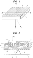
- Fig. 1 is a perspective view for indicating a diffractive optical element which performs a polization separation operation, according to an embodiment 1 of the present invention.
- a diffraction grating 3 capable of performing the polirization separation operation is provided on a substrate 2.
- the diffraction grating 3 is constituted by an one-dimensional blazed type grating shape, and has a grating period "Pt" along a direction of 2 - 2 shown in this drawing.
- diffraction directions of light beams incident on diffractive optical element 1 are made different from each other, depending upon polarization directions thereof. Further, this diffraction grating 3 is set in such a manner that each of polarized lights is diffracted only at a specific diffraction order.
- Fig. 2 is an explanatory diagram for explaining a portion of a sectional shape of the diffractive optical element 1 of Fig. 1, cut away at the line 2 - 2 of Fig. 1.
- a sectional grating shape of the diffraction grating 3 which constitutes the diffractive optical element 1 according to the present invention is arranged by a blazed type first diffraction grating portion 4 which is provided on the substrate 2, and by a blazed type second diffraction grating portion 5 which is formed on the first diffraction grating portion 4.
- an entire surface of light incident surface of this diffraction grating portion is constituted by an SWS grating (Sub-Wavelength structured grating) which has a minute periodic structure which is smaller than a wavelength of light under use.
- SWS grating Sub-Wavelength structured grating
- all of the first and second diffraction grating portions 4 and 5 may function as such a diffractive optical element that executes a single polarization separating operation.
- the diffraction grating 3 formed on the substrate 2 is formed at a boundary between a material n1( ⁇ ) and another material n2( ⁇ ).
- the first diffraction grating portion 4 is made of the material n2( ⁇ ), and corresponds to an one-dimensional diffraction grating portion having a sawtooth shape, the grating pitch of which is "Pt” and the grating thickness of which is "d1.”
- the second diffraction grating portion 5 has an SWS grating structure in which the material n1( ⁇ ) and the material n2( ⁇ ) are alternatively repeated with a minute period smaller than the wavelength the light used.
- the grating pitch of the SWS grating is "P1"
- this second diffraction grating portion 5 is such an one-dimensional rectangular grating shape having a period parallel to the grating pitch "Pt" of the first diffraction grating portion 4.
- the grating thickness of this SWS grating is varied from a thickness of (d1 + D + d2) to another thickness of (D) in a monotone mode along a periodic direction, and this thickness change is repeated with the period of the above-explained grating pitch "Pt".
- both the grating pitch "p1" and the filling factor "F" of the SWS grating are always constant value.
- the structure of the diffractive optical element according to this embodiment 1 will now be described based upon concrete numerical values.
- the period In order that a minute periodic structure acts as an SWS grating, the period must be sufficiently made smaller with respect to a used wavelength.
- n2( ⁇ ) sin ⁇ 2 - n1( ⁇ ) sin ⁇ 1 m ⁇ / p1
- symbols n1( ⁇ ) and n2( ⁇ ) indicate refractive indexes of materials (qualities of used members) at light incident side/light exit side in the diffractive optical element
- symbol “ ⁇ 1” shows an incident angle of a light beam
- symbol “ ⁇ 2” indicates an exit angle (diffraction angle) of the light beam
- symbol “m” represents a diffraction order
- symbol “ ⁇ ” shows a used wavelength
- symbol “p1” denotes a period (pitch) of a minute periodic structure.
- a diffractive optical element is applied to a part of an optical system, it is preferable to select a pitch "p1" that only zero-order diffraction light as a light traveling therefrom can be established.
- the period "p1" of the minute periodic structure is equal to 0.27 ⁇ m based upon the above-explained formula (1).
- the propagated or traveled light beam is only zero-order diffraction light with respect to the minute periodic structure.
- the minute periodic structure may have the form birefringence corresponding to the specific characteristic as the SWS grating.
- a refractive index of an optical wave which is vibrated in parallel to an extension direction of the minute periodic structure namely, will be referred to as "P-polarized light” hereinafter
- S-polarized light a refractive index of an optical wave which is vibrated perpendicular to this extension direction
- the second diffraction grating portion 5 may be functioned as different diffraction gratings with respect to the P-polarized light and the S-polarized light.
- a polarization separation operation may be obtained as follows: That is, the P-polarized light travels straight on as zero-order diffraction light, whereas the S-polarized light is diffracted as first-order diffraction light to one given direction. Also, since this condition is established, no diffraction occurs in the SWS grating.
- a diffraction separation operation is performed as the diffractive optical element capable of performing the polarization separation operation, no care is taken into the occurrence of diffraction in the minute periodic structure.
- the minute period in order that the period (pitch) of the minute periodic structure can satisfy the above-described conditions, the minute period must be determined in such a manner that this condition can be satisfied within the range of the range of the used incident angle over the entire region of wavelengths used.
- Fig. 3 represents a polarization separation characteristic which is achieved by the polarization separation element having the above-explained minute periodic structure.
- This embodiment is arranged as follows: That is, the P-polarized light component of the incident light beam is separated as the zero-order diffraction light of the one-dimensional diffractive optical element constituted by the grating pitch "Pt", and the S-polarized light component of the incident light beam is separated as the first-order diffraction light.
- the material 1 is made of air
- the grating thickness d1 is 2.32 ⁇ m
- the grating thickness d2 is 3.88 ⁇ m
- the thickness D is 0.5 ⁇ m.
- both the P-polarized light component and the S-polarized light component can own better characteristics higher than, or equal to approximately 98% over the visible light range.
- the diffraction grating 3 is provided on the substrate 2.
- a substrate made of a quartz is employed, and a shape may be directly formed on the substrate by way of an etching treatment using the quartz substrate and the like.
- an essential material may be realized only by one sort of quartz.
- the period of the minute periodic structure is set in parallel to the period of the diffraction grating portion.
- the present invention is not limited to this structure, but may be realized by that the period of the diffraction grating portion may be set perpendicular to the period of the minute periodic structure.
- Fig. 4 is a sectional view for showing a major structure of a diffractive optical element according to an embodiment 2 of the present invention.
- the diffractive optical element of this embodiment 2 is featured by such a structure that an edge surface of a minute periodic grating provided on a light incidence side is matched with a grating periodic direction in parallel with each other.
- both the grating pitch "P1" of the minute periodic structure and the filling factor F f1 / P1 have the constant values.
- a filling factor Fs Ps / fs is changed with the grating pitch "Pt" of the second diffraction grating portion 5 in order to make the edge surfaces parallel to each other.
- a value of a filling factor is made larger at the deeper portion in the SWS grating, whereas a value of a filling factor is made smaller or at the thinner in the SWS grating.
- this diffractive element is made of 9 sets of minute gratings within the grating pitch "Pt".
- the above-explained relationship may be expressed as : F1 > F2 > F3 > F4 > F5 > F6 > F7 > F8 > F9, Fs; 1 ⁇ s ⁇ 9.
- the thin SWS grating since a ratio of a material 2 becomes small with respect to air of a material 1, an apparent refractive index is approximated to air of the material 1.
- the grating thickness of the deep grating can be made relatively thinner. Since the filling factors are optimized, such a structure can be made that the edge surface of the minute periodic grating formed on the light incidence side is matched with the grating periodic direction in parallel to each other. As to this structure, in such a case that the SWS grating is formed by way of an etching treatment, since an etching mask may be close-contacted thereto, the minute periodic structure having the superior performance can be manufactured.
- the grating pitch of the SWS grating may be gradually changed.
- the grating pitch is made larger within a range where the SWS grating can be established along such a direction that the grating becomes thinner, so that it is possible to suppress such a condition that the absolute width of the material 2 of the rectangular grating becomes narrow. This is very preferable in view of the manufacturing aspect.
- Fig. 5 is a schematic diagram for indicating a major portion of a diffractive optical element according to a third embodiment of the present invention.
- the diffractive optical element of this third embodiment is featured by that the grating shape of the first diffraction grating portion 4 according to the embodiment 2 is made in a stepped grating. Also, a filling factor Fs of an SWS grating along a grating periodic direction is changed in response to the step configuration.
- the diffractive optical element is arranged in such a manner that 8 sets of minute gratings are provided within the grating pitch Pt.
- the stepped grating has four stages of stepped shapes.
- the diffractive optical element may be manufactured by way of an etching technique in a relatively simple manner.
- the filling factor Fs is not changed along the above-explained grating periodic direction in correspondence with the stepped shape, but the filling factor may be changed along the depth direction.
- Fs corresponds to an occupation ratio of the material 2 within the grating pitch Ps.
- the filling factor Fs is changed as 2 stages, 3 stages, ---, n stages in response to the depth, while the stepped grating is set along the height direction (depth direction).
- Fig. 7 is an explanatory diagram for explaining a structure of a polarization converting element, according to an embodiment 1, by using the diffractive optical element for performing the polarization separation of the present invention.
- a light beam "La” having random polarization direction is incident on a diffraction grating 3 formed on a substrate 2.
- the light beam “La” is entered from an opening portion A1 formed in a light shielding member 6.
- a P-polarized light component "P” is not diffracted so that zero-order diffraction light, travels straight on, whereas an S-polarized light component "S” is diffracted/separated as first-order diffraction light.
- the polarization direction of this P-polarized light component is converted into on S-polarized component by a 1/2-wavelength plate 8 provided on the exit side, and then the S-polarized light component is emerges therefrom.
- the diffracted S-polarized light component is diffracted by the diffraction grating 3 so as to emerge as S-polarized light component therefrom toward the same direction as the light beam passing through the 1/2-wavelength plate 8.
- the light beam La having the random polarization directions enters into the diffractive optical element, the light beam the polarization direction of which has become uniform emerges as S-polarized light therefrom.
- this structure may be preferably manufactured by way of the same manufacturing method as that of the diffractive optical element 1.
- the emergence direction of any one of the light beames namely either the P-polarized light light beam or the S-polarized light light beam which is diffracted in a given direction depending on the polarization direction and separated from the other polarized light beam is made coincident with the emergence direction of the other S-polarized light or P-polarized light.
- the deflecting means 7 has a function of an optical member by which the incident direction of the light beam incident on the diffractive optical element 1 is made substantially parallel to the emergence direction thereof.
- each of the diffractive optical elements is arranged in such a manner that this diffractive optical element has the grating structure in which at least two kinds of diffraction gratings are overlapped with each other, and also at least one kind of diffraction grating portion of these diffraction gratings has the minute periodic structure smaller than the used wavelength, so that the diffraction direction differs depending upon the polarization direction of the light beam incident on the diffractive optical element and each of the polarized light beam incident thereon is diffracted at only a predetermined diffraction order, within the entire range of these used wavelengths.
- each of the diffractive optical elements may be used in the similar utilization field to the conventional thin-film, and also the superior incident angle characteristic owned by the SWS grating itself may be effectively utilized.
- each of the diffractive optical elements is applied to the polarization converting element, it is possible to realize such a high-precision polarization converting element having a simple structure.
- Fig. 12 is a schematic diagram for representing a major arrangement of a projection apparatus with employment of the polarization converting element according to the present invention.
- symbol 12 indicates a light source unit which emits a light beam containing an S-polarized light component and a P-polarized light component.
- reference numeral 11 indicates a reflection mirror.
- the reflection mirror 11 reflects the light beam emitted from the light source unit 12 toward a direction opposed to the polarization converting element 13 side.
- the polarization converting element 13 has the structure as previously explained in Fig. 7. This polarization converting element 13 causes the light beam emitted from the light source unit 12 to emerge as a light beam having any one of the polarization directions which are S-polarized state and P-polarized state.
- Reference numeral 14 represents an optical modulating means (liquid crystal panel) comprising a liquid crystal display (LCD) device which modulates the light emerging from the polarization converting element 13 on the basis of a supplied image signal.
- reference numeral 16 shows a projection optical system.
- the projection optical system 16 projects the light beam modulated by the optical modulating means 14 onto a screen 17 so as to form an image on this screen 17.
- the image signal supplied to the modulating means 14 is controlled by an image processing means 18 such as a personal computer or the like.
- the diffraction is effected depending on the polarization direction of the light beam incident thereon so as to produce a diffracted light with a predetermined diffraction order only.
- Both the diffractive optical element and the polarization converting element using this diffractive optical element can be realized which may be utilized in a similar manner to the polarization separation element having the thin-film structure.
- both the diffractive optical element and the polarization converting element using this diffractive optical element can be realized, which own the SWS grating structures manufactured under better conditions, also may perform the polarization separation operation.
Applications Claiming Priority (2)
| Application Number | Priority Date | Filing Date | Title |
|---|---|---|---|
| JP2000162572 | 2000-05-31 | ||
| JP2000162572A JP2001343512A (ja) | 2000-05-31 | 2000-05-31 | 回折光学素子及びそれを有する光学系 |
Publications (2)
| Publication Number | Publication Date |
|---|---|
| EP1160589A1 true EP1160589A1 (de) | 2001-12-05 |
| EP1160589B1 EP1160589B1 (de) | 2005-10-19 |
Family
ID=18666455
Family Applications (1)
| Application Number | Title | Priority Date | Filing Date |
|---|---|---|---|
| EP01304753A Expired - Lifetime EP1160589B1 (de) | 2000-05-31 | 2001-05-30 | Optisches Beugungselement und damit ausgestattetes optisches System |
Country Status (4)
| Country | Link |
|---|---|
| US (1) | US7075722B2 (de) |
| EP (1) | EP1160589B1 (de) |
| JP (1) | JP2001343512A (de) |
| DE (1) | DE60114086T2 (de) |
Cited By (15)
| Publication number | Priority date | Publication date | Assignee | Title |
|---|---|---|---|---|
| WO2004102233A1 (de) * | 2003-05-17 | 2004-11-25 | Carl-Zeiss-Stiftung Trading As Carl Zeiss | Diffraktives optisches element sowie projektionsobjektiv mit einem solchen element |
| EP1486803A2 (de) * | 2003-05-06 | 2004-12-15 | Light Impressions International Limited | Optische doppelbrechende Struktur mit variabler Form, Methode für deren Herstellung, System und Methode zur deren Erkennung |
| WO2006008666A1 (en) * | 2004-07-13 | 2006-01-26 | Koninklijke Philips Electronics N.V. | Polarizing device |
| US7139127B2 (en) | 2002-08-24 | 2006-11-21 | Carl Zeiss Ag | Diffractive optical element |
| DE102005036158A1 (de) * | 2005-07-26 | 2007-02-08 | Jenoptik Laser, Optik, Systeme Gmbh | Anordnung und Verfahren zur Umwandlung einer primären, unpolarisierten Strahlungsintensitätsverteilung in eine vorgegebene, raumwinkelabhängig polarisierte Intensitätsverteilung |
| WO2008012091A2 (de) * | 2006-07-28 | 2008-01-31 | Carl Zeiss Smt Ag | Verfahren und vorrichtung zum bestimmen einer abweichung einer tatsächlichen form von einer sollform einer optischen oberfläche |
| WO2009036941A2 (de) * | 2007-09-20 | 2009-03-26 | Carl Zeiss Ag | Binär geblazetes diffraktives optisches element |
| WO2010063737A1 (en) * | 2008-12-01 | 2010-06-10 | Optaglio, S.R.O. | Optical device and method of manufacture |
| US7936521B2 (en) | 2007-07-09 | 2011-05-03 | Carl Zeiss Smt Gmbh | Method of measuring a deviation of an optical surface from a target shape |
| US8068279B2 (en) | 2006-03-14 | 2011-11-29 | Carl Zeiss Smt Gmbh | Optical system of an illumination device of a projection exposure apparatus |
| CN107179576A (zh) * | 2017-06-05 | 2017-09-19 | 苏州大学 | 一种可见光波段的渐变相位金属光栅 |
| WO2019209527A1 (en) * | 2018-04-23 | 2019-10-31 | Facebook Technologies, Llc | Gratings with variable depths for waveguide displays |
| US10649141B1 (en) | 2018-04-23 | 2020-05-12 | Facebook Technologies, Llc | Gratings with variable etch heights for waveguide displays |
| US10732351B2 (en) | 2018-04-23 | 2020-08-04 | Facebook Technologies, Llc | Gratings with variable depths formed using planarization for waveguide displays |
| US10809448B1 (en) | 2019-04-18 | 2020-10-20 | Facebook Technologies, Llc | Reducing demolding stress at edges of gratings in nanoimprint lithography |
Families Citing this family (65)
| Publication number | Priority date | Publication date | Assignee | Title |
|---|---|---|---|---|
| US6930053B2 (en) | 2002-03-25 | 2005-08-16 | Sanyo Electric Co., Ltd. | Method of forming grating microstructures by anodic oxidation |
| JP4250906B2 (ja) * | 2002-04-23 | 2009-04-08 | コニカミノルタホールディングス株式会社 | 光学素子 |
| DE10313548B4 (de) * | 2002-08-24 | 2012-09-06 | Carl Zeiss Smt Gmbh | Binär geblazetes diffraktives optisches Element sowie ein solches Element enthaltendes Objektiv |
| US6747785B2 (en) * | 2002-10-24 | 2004-06-08 | Hewlett-Packard Development Company, L.P. | MEMS-actuated color light modulator and methods |
| DE10322239B4 (de) * | 2003-05-17 | 2011-06-30 | Carl Zeiss SMT GmbH, 73447 | Geblazetes diffraktives optisches Element sowie Projektionsobjektiv mit einem solchen Element |
| DE10324468B4 (de) * | 2003-05-30 | 2006-11-09 | Carl Zeiss Smt Ag | Mikrolithografische Projektionsbelichtungsanlage, Projektionsobjektiv hierfür sowie darin enthaltenes optisches Element |
| US7239448B2 (en) * | 2003-10-27 | 2007-07-03 | Matsushita Electric Industrial Co., Ltd | Light quantity distribution control element and optical apparatus using the same |
| TWI230834B (en) * | 2003-12-31 | 2005-04-11 | Ind Tech Res Inst | High-transmissivity polarizing module constituted with sub-wavelength structure |
| CN100376958C (zh) * | 2004-02-19 | 2008-03-26 | 鸿富锦精密工业(深圳)有限公司 | 导光板及背光模组 |
| JP4951209B2 (ja) * | 2004-03-31 | 2012-06-13 | パナソニック株式会社 | 色分離装置及び撮像装置 |
| JP2005322849A (ja) * | 2004-05-11 | 2005-11-17 | Nec Compound Semiconductor Devices Ltd | 半導体レーザおよびその製造方法 |
| US20060001969A1 (en) * | 2004-07-02 | 2006-01-05 | Nanoopto Corporation | Gratings, related optical devices and systems, and methods of making such gratings |
| DE102004040535A1 (de) * | 2004-08-20 | 2006-02-23 | Carl Zeiss Ag | Polarisationsselektiv geblazetes diffraktives optisches Element |
| JP2006114201A (ja) * | 2004-09-14 | 2006-04-27 | Hitachi Maxell Ltd | 偏光回折素子及び光ヘッド装置 |
| JP2006126338A (ja) * | 2004-10-27 | 2006-05-18 | Nippon Sheet Glass Co Ltd | 偏光子およびその製造方法 |
| US7800823B2 (en) * | 2004-12-06 | 2010-09-21 | Moxtek, Inc. | Polarization device to polarize and further control light |
| US7570424B2 (en) * | 2004-12-06 | 2009-08-04 | Moxtek, Inc. | Multilayer wire-grid polarizer |
| US7630133B2 (en) * | 2004-12-06 | 2009-12-08 | Moxtek, Inc. | Inorganic, dielectric, grid polarizer and non-zero order diffraction grating |
| US7961393B2 (en) * | 2004-12-06 | 2011-06-14 | Moxtek, Inc. | Selectively absorptive wire-grid polarizer |
| US20060127830A1 (en) * | 2004-12-15 | 2006-06-15 | Xuegong Deng | Structures for polarization and beam control |
| US7619816B2 (en) * | 2004-12-15 | 2009-11-17 | Api Nanofabrication And Research Corp. | Structures for polarization and beam control |
| US8263194B2 (en) * | 2004-12-30 | 2012-09-11 | Industrial Technology Research Institute | Color filter and method of fabricating the same |
| TWI259913B (en) * | 2004-12-30 | 2006-08-11 | Ind Tech Res Inst | Color filter and methods of making the same |
| JP2006301113A (ja) * | 2005-04-18 | 2006-11-02 | Ricoh Co Ltd | マルチビーム光源ユニット・光走査装置・画像形成装置・光ビーム合成素子・光学系・光学機器 |
| JP4336665B2 (ja) | 2005-05-12 | 2009-09-30 | 株式会社エンプラス | 光学素子およびこれを備えた光ピックアップ装置 |
| JP2006323059A (ja) * | 2005-05-18 | 2006-11-30 | Konica Minolta Holdings Inc | 構造性複屈折波長板及び波長板組合せ構造 |
| JP2007033676A (ja) * | 2005-07-25 | 2007-02-08 | Ricoh Co Ltd | 偏光変換光学素子、光変調モジュール及び投射型画像表示装置 |
| US20090190068A1 (en) * | 2005-09-22 | 2009-07-30 | Sharp Kabushiki Kaisha | Light guiding body, substrate for display device, and display device |
| US7529048B2 (en) * | 2006-03-03 | 2009-05-05 | Ching-Bin Lin | Optical film having multi-story prisms and manufacturing process thereof |
| JP2007328096A (ja) * | 2006-06-07 | 2007-12-20 | Ricoh Co Ltd | 回折光学素子とその作製方法および光学モジュール |
| JP5024859B2 (ja) * | 2006-06-14 | 2012-09-12 | 株式会社リコー | 画像表示装置 |
| US8755113B2 (en) * | 2006-08-31 | 2014-06-17 | Moxtek, Inc. | Durable, inorganic, absorptive, ultra-violet, grid polarizer |
| EP2118693A4 (de) * | 2007-02-23 | 2011-08-10 | Nanocomp Ltd | Verfahren zum entwurf einer beugungsgitterstruktur und beugungsgitterstruktur |
| US20080316599A1 (en) * | 2007-06-22 | 2008-12-25 | Bin Wang | Reflection-Repressed Wire-Grid Polarizer |
| US8493658B2 (en) * | 2007-07-06 | 2013-07-23 | Semiconductor Energy Laboratory Co., Ltd. | Polarizer and display device including polarizer |
| JP2009103915A (ja) * | 2007-10-23 | 2009-05-14 | Fuji Xerox Co Ltd | 光導波路フィルム及びその製造方法、並びに、光送受信モジュール |
| JP4535121B2 (ja) * | 2007-11-28 | 2010-09-01 | セイコーエプソン株式会社 | 光学素子及びその製造方法、液晶装置、電子機器 |
| JP5391670B2 (ja) * | 2007-12-27 | 2014-01-15 | セイコーエプソン株式会社 | 微細構造体の製造方法 |
| DE102008005817A1 (de) * | 2008-01-24 | 2009-07-30 | Carl Zeiss Ag | Optisches Anzeigegerät |
| JP4968234B2 (ja) * | 2008-10-21 | 2012-07-04 | セイコーエプソン株式会社 | 光学素子及び表示装置 |
| US20100103517A1 (en) * | 2008-10-29 | 2010-04-29 | Mark Alan Davis | Segmented film deposition |
| JP5218079B2 (ja) | 2009-01-15 | 2013-06-26 | 株式会社リコー | 光学素子、光ピックアップ、光情報処理装置、光減衰器、偏光変換素子、プロジェクタ光学系、光学機器 |
| JP2010164752A (ja) * | 2009-01-15 | 2010-07-29 | Ricoh Co Ltd | 光学素子、光ピックアップ、光情報処理装置、光減衰器、偏光変換素子、プロジェクタ光学系、光学機器 |
| US8248696B2 (en) * | 2009-06-25 | 2012-08-21 | Moxtek, Inc. | Nano fractal diffuser |
| JP5604860B2 (ja) * | 2009-12-16 | 2014-10-15 | 凸版印刷株式会社 | 偽造防止用紙 |
| JP5188524B2 (ja) * | 2010-03-05 | 2013-04-24 | キヤノン株式会社 | 偏光分離素子 |
| US8913321B2 (en) | 2010-09-21 | 2014-12-16 | Moxtek, Inc. | Fine pitch grid polarizer |
| US8611007B2 (en) | 2010-09-21 | 2013-12-17 | Moxtek, Inc. | Fine pitch wire grid polarizer |
| JP5632760B2 (ja) * | 2011-01-20 | 2014-11-26 | 日本板硝子株式会社 | 無機偏光ブレーズド回折格子 |
| KR20140031909A (ko) * | 2011-04-28 | 2014-03-13 | 바스프 에스이 | 태양광 관리용 ir 반사체 |
| US8913320B2 (en) | 2011-05-17 | 2014-12-16 | Moxtek, Inc. | Wire grid polarizer with bordered sections |
| US8873144B2 (en) | 2011-05-17 | 2014-10-28 | Moxtek, Inc. | Wire grid polarizer with multiple functionality sections |
| AU2011100725B4 (en) * | 2011-06-17 | 2011-09-22 | Innovia Security Pty Ltd | Diffraction grating |
| DE102011084055B4 (de) * | 2011-10-05 | 2015-12-17 | Fraunhofer-Gesellschaft zur Förderung der angewandten Forschung e.V. | Optischer filter mit einem resonanten wellenleitergitter |
| EP2802861A4 (de) * | 2012-01-11 | 2015-08-19 | Hughes Howard Med Inst | Mehrdimensionale bildgebung mit multifokaler mikroskopie |
| US8922890B2 (en) | 2012-03-21 | 2014-12-30 | Moxtek, Inc. | Polarizer edge rib modification |
| US8948549B2 (en) * | 2012-11-27 | 2015-02-03 | Teraxion Inc. | Polarization rotator assembly including a subwavelength composite portion |
| WO2014133481A1 (en) * | 2013-02-26 | 2014-09-04 | Hewlett-Packard Development Company, L.P. | Multiview 3d telepresence |
| US9632223B2 (en) | 2013-10-24 | 2017-04-25 | Moxtek, Inc. | Wire grid polarizer with side region |
| DE102014219663A1 (de) * | 2014-09-29 | 2016-03-31 | Ihp Gmbh - Innovations For High Performance Microelectronics / Leibniz-Institut Für Innovative Mikroelektronik | Photonisch integrierter Chip, optisches Bauelement mit photonisch integriertem Chip und Verfahren zu deren Herstellung |
| WO2018075174A1 (en) * | 2016-10-18 | 2018-04-26 | Molecular Imprints, Inc. | Microlithographic fabrication of structures |
| KR20200017017A (ko) * | 2018-08-07 | 2020-02-18 | 삼성전자주식회사 | 구조광 프로젝터 및 이를 포함하는 전자 장치 |
| CN109459865B (zh) * | 2018-11-20 | 2024-03-26 | 成都航空职业技术学院 | 一种3d显示装置 |
| US11448918B2 (en) * | 2019-01-30 | 2022-09-20 | Samsung Electronics Co., Ltd. | Grating device, screen including the grating device, method of manufacturing the screen and display apparatus for augmented reality and/or virtual reality including the screen |
| CN115629485B (zh) * | 2022-12-07 | 2023-05-12 | 合肥的卢深视科技有限公司 | 散斑投射器和结构光相机 |
Citations (6)
| Publication number | Priority date | Publication date | Assignee | Title |
|---|---|---|---|---|
| EP0383307A2 (de) * | 1989-02-15 | 1990-08-22 | Canon Kabushiki Kaisha | Bildabtastvorrichtung |
| US5122903A (en) * | 1989-03-15 | 1992-06-16 | Omron Corporation | Optical device and optical pickup device using the same |
| EP0821258A2 (de) * | 1996-07-25 | 1998-01-28 | Seiko Epson Corporation | Optisches Element für Projektionsanzeigevorrichtung |
| EP0898182A2 (de) * | 1997-08-20 | 1999-02-24 | Canon Kabushiki Kaisha | Diffraktives optisches Element und optisches System unter Verwendung desselben |
| US5914811A (en) * | 1996-08-30 | 1999-06-22 | University Of Houston | Birefringent grating polarizing beam splitter |
| US6046851A (en) * | 1996-09-06 | 2000-04-04 | Nec Corporation | Polarization beam splitter and method for making the same |
Family Cites Families (11)
| Publication number | Priority date | Publication date | Assignee | Title |
|---|---|---|---|---|
| US5115423A (en) * | 1988-01-07 | 1992-05-19 | Ricoh Company, Ltd. | Optomagnetic recording/reproducing apparatus |
| US5015835A (en) * | 1988-12-23 | 1991-05-14 | Ricoh Company, Ltd. | Optical information reading and writing device with diffraction means |
| JPH02214372A (ja) | 1989-02-15 | 1990-08-27 | Canon Inc | カラー画像読取り装置 |
| JP3396890B2 (ja) * | 1992-02-21 | 2003-04-14 | 松下電器産業株式会社 | ホログラム、これを用いた光ヘッド装置及び光学系 |
| US5956302A (en) * | 1993-08-17 | 1999-09-21 | Ricoh Company, Ltd. | Optical pick-up device and method using a high-density double diffraction grating |
| US5561558A (en) * | 1993-10-18 | 1996-10-01 | Matsushita Electric Industrial Co., Ltd. | Diffractive optical device |
| US5581405A (en) * | 1993-12-29 | 1996-12-03 | Eastman Kodak Company | Hybrid refractive/diffractive achromatic camera lens and camera using such |
| EP0730746A1 (de) * | 1994-05-02 | 1996-09-11 | Koninklijke Philips Electronics N.V. | Optisches lichtdurchlässiges bauelement mit antireflektionsgittern |
| IL115295A0 (en) * | 1995-09-14 | 1996-12-05 | Yeda Res & Dev | Multilevel diffractive optical element |
| JPH1039136A (ja) | 1996-07-25 | 1998-02-13 | Seiko Epson Corp | 光学素子および投写型表示装置 |
| US6317268B1 (en) * | 1999-11-23 | 2001-11-13 | Eastman Kodak Company | Movie projection lens |
-
2000
- 2000-05-31 JP JP2000162572A patent/JP2001343512A/ja active Pending
-
2001
- 2001-05-30 US US09/866,587 patent/US7075722B2/en not_active Expired - Fee Related
- 2001-05-30 EP EP01304753A patent/EP1160589B1/de not_active Expired - Lifetime
- 2001-05-30 DE DE60114086T patent/DE60114086T2/de not_active Expired - Lifetime
Patent Citations (6)
| Publication number | Priority date | Publication date | Assignee | Title |
|---|---|---|---|---|
| EP0383307A2 (de) * | 1989-02-15 | 1990-08-22 | Canon Kabushiki Kaisha | Bildabtastvorrichtung |
| US5122903A (en) * | 1989-03-15 | 1992-06-16 | Omron Corporation | Optical device and optical pickup device using the same |
| EP0821258A2 (de) * | 1996-07-25 | 1998-01-28 | Seiko Epson Corporation | Optisches Element für Projektionsanzeigevorrichtung |
| US5914811A (en) * | 1996-08-30 | 1999-06-22 | University Of Houston | Birefringent grating polarizing beam splitter |
| US6046851A (en) * | 1996-09-06 | 2000-04-04 | Nec Corporation | Polarization beam splitter and method for making the same |
| EP0898182A2 (de) * | 1997-08-20 | 1999-02-24 | Canon Kabushiki Kaisha | Diffraktives optisches Element und optisches System unter Verwendung desselben |
Cited By (32)
| Publication number | Priority date | Publication date | Assignee | Title |
|---|---|---|---|---|
| US7139127B2 (en) | 2002-08-24 | 2006-11-21 | Carl Zeiss Ag | Diffractive optical element |
| EP1486803A2 (de) * | 2003-05-06 | 2004-12-15 | Light Impressions International Limited | Optische doppelbrechende Struktur mit variabler Form, Methode für deren Herstellung, System und Methode zur deren Erkennung |
| EP1486803A3 (de) * | 2003-05-06 | 2005-03-16 | Light Impressions International Limited | Optische doppelbrechende Struktur mit variabler Form, Methode für deren Herstellung, System und Methode zur deren Erkennung |
| WO2004102233A1 (de) * | 2003-05-17 | 2004-11-25 | Carl-Zeiss-Stiftung Trading As Carl Zeiss | Diffraktives optisches element sowie projektionsobjektiv mit einem solchen element |
| US7453643B2 (en) | 2003-05-17 | 2008-11-18 | Carl Zeiss Smt Ag | Blazed diffractive optical element and projection objective for a microlithographic projection exposure apparatus |
| WO2006008666A1 (en) * | 2004-07-13 | 2006-01-26 | Koninklijke Philips Electronics N.V. | Polarizing device |
| DE102005036158B4 (de) * | 2005-07-26 | 2011-01-13 | Jenoptik Laser, Optik, Systeme Gmbh | Anordnung und Verfahren zur Umwandlung einer primären, unpolarisierten Strahlungsintensitätsverteilung in eine vorgegebene, raumwinkelabhängig polarisierte Intensitätsverteilung |
| DE102005036158A1 (de) * | 2005-07-26 | 2007-02-08 | Jenoptik Laser, Optik, Systeme Gmbh | Anordnung und Verfahren zur Umwandlung einer primären, unpolarisierten Strahlungsintensitätsverteilung in eine vorgegebene, raumwinkelabhängig polarisierte Intensitätsverteilung |
| US8068279B2 (en) | 2006-03-14 | 2011-11-29 | Carl Zeiss Smt Gmbh | Optical system of an illumination device of a projection exposure apparatus |
| US8104905B2 (en) | 2006-07-28 | 2012-01-31 | Carl Zeiss Smt Gmbh | Method and apparatus for determining a deviation of an actual shape from a desired shape of an optical surface |
| WO2008012091A3 (de) * | 2006-07-28 | 2008-03-13 | Zeiss Carl Smt Ag | Verfahren und vorrichtung zum bestimmen einer abweichung einer tatsächlichen form von einer sollform einer optischen oberfläche |
| CN101495833B (zh) * | 2006-07-28 | 2013-08-28 | 卡尔蔡司Smt有限责任公司 | 确定光学表面的实际形状偏离理想形状的偏差的方法和装置 |
| US8345262B2 (en) | 2006-07-28 | 2013-01-01 | Carl Zeiss Smt Gmbh | Method and apparatus for determining a deviation of an actual shape from a desired shape of an optical surface |
| WO2008012091A2 (de) * | 2006-07-28 | 2008-01-31 | Carl Zeiss Smt Ag | Verfahren und vorrichtung zum bestimmen einer abweichung einer tatsächlichen form von einer sollform einer optischen oberfläche |
| US8089634B2 (en) | 2007-07-09 | 2012-01-03 | Carl Zeiss Smt Gmbh | Optical element and method of calibrating a measuring apparatus comprising a wave shaping structure |
| US7936521B2 (en) | 2007-07-09 | 2011-05-03 | Carl Zeiss Smt Gmbh | Method of measuring a deviation of an optical surface from a target shape |
| US8264695B2 (en) | 2007-07-09 | 2012-09-11 | Carl Zeiss Smt Gmbh | Method of measuring a deviation of an optical surface from a target shape |
| US8508749B2 (en) | 2007-07-09 | 2013-08-13 | Carl Zeiss Smt Gmbh | Method of measuring a deviation of an optical surface from a target shape using interferometric measurement results |
| WO2009036941A3 (de) * | 2007-09-20 | 2009-05-28 | Zeiss Carl Ag | Binär geblazetes diffraktives optisches element |
| WO2009036941A2 (de) * | 2007-09-20 | 2009-03-26 | Carl Zeiss Ag | Binär geblazetes diffraktives optisches element |
| WO2010063737A1 (en) * | 2008-12-01 | 2010-06-10 | Optaglio, S.R.O. | Optical device and method of manufacture |
| CN107179576A (zh) * | 2017-06-05 | 2017-09-19 | 苏州大学 | 一种可见光波段的渐变相位金属光栅 |
| CN107179576B (zh) * | 2017-06-05 | 2019-08-23 | 苏州大学 | 一种可见光波段的渐变相位金属光栅 |
| WO2019209527A1 (en) * | 2018-04-23 | 2019-10-31 | Facebook Technologies, Llc | Gratings with variable depths for waveguide displays |
| US10649141B1 (en) | 2018-04-23 | 2020-05-12 | Facebook Technologies, Llc | Gratings with variable etch heights for waveguide displays |
| US10732351B2 (en) | 2018-04-23 | 2020-08-04 | Facebook Technologies, Llc | Gratings with variable depths formed using planarization for waveguide displays |
| US11067726B2 (en) | 2018-04-23 | 2021-07-20 | Facebook Technologies, Llc | Gratings with variable depths for waveguide displays |
| US11175455B1 (en) | 2018-04-23 | 2021-11-16 | Facebook Technologies, Llc | Gratings with variable etch heights for waveguide displays |
| US11402578B2 (en) | 2018-04-23 | 2022-08-02 | Meta Platforms Technologies, Llc | Gratings with variable depths formed using planarization for waveguide displays |
| US11579364B2 (en) | 2018-04-23 | 2023-02-14 | Meta Platforms Technologies, Llc | Gratings with variable depths formed using planarization for waveguide displays |
| US10809448B1 (en) | 2019-04-18 | 2020-10-20 | Facebook Technologies, Llc | Reducing demolding stress at edges of gratings in nanoimprint lithography |
| WO2020214186A1 (en) * | 2019-04-18 | 2020-10-22 | Facebook Technologies, Llc | Reducing demolding stress at edges of gratings in nanoimprint lithography |
Also Published As
| Publication number | Publication date |
|---|---|
| JP2001343512A (ja) | 2001-12-14 |
| DE60114086D1 (de) | 2006-03-02 |
| EP1160589B1 (de) | 2005-10-19 |
| US20020003661A1 (en) | 2002-01-10 |
| US7075722B2 (en) | 2006-07-11 |
| DE60114086T2 (de) | 2006-05-24 |
Similar Documents
| Publication | Publication Date | Title |
|---|---|---|
| EP1160589B1 (de) | Optisches Beugungselement und damit ausgestattetes optisches System | |
| JP4475501B2 (ja) | 分光素子、回折格子、複合回折格子、カラー表示装置、および分波器 | |
| US6927915B2 (en) | Diffractive optical element, and optical system and optical apparatus provided with the same | |
| US7301700B2 (en) | Polarization beam splitter and optical system using the same, and image displaying apparatus, using the same | |
| US7236655B2 (en) | Polarization element and optical device using polarization element | |
| US6947215B2 (en) | Optical element, optical functional device, polarization conversion device, image display apparatus, and image display system | |
| KR101226346B1 (ko) | 광학 소자, 광학 장치, 광 픽업, 광 정보 처리 장치, 광 감쇠기, 편광 변환 소자, 프로젝터 광학 시스템 및 광학 장치 시스템 | |
| US7894133B2 (en) | Optical element and optical device | |
| EP3710894A1 (de) | Verfahren zur herstellung von lichtwellenleitern | |
| WO2012140845A1 (ja) | インコヒーレント化デバイス、およびこれを用いた光学装置 | |
| JP4125114B2 (ja) | 光学素子、光学変調素子、画像表示装置 | |
| JP2011154078A (ja) | 液晶表示装置 | |
| JP2000241812A (ja) | 透過型液晶表示装置 | |
| JP3412706B2 (ja) | 光合分波装置 | |
| KR20010043706A (ko) | 회절선택적인 편광빔 스플리터 및 이 스플리터에 의해제조된 빔 경로 선택 프리즘 | |
| JPH08220531A (ja) | 液晶表示装置 | |
| JP2012013931A (ja) | 平面導波路 | |
| JP2002182026A (ja) | 光学素子およびそれを用いた分光装置 | |
| JP2001296424A (ja) | 偏光素子 | |
| JPH02291507A (ja) | 二次元光導波路型te,tmモードスプリッタ |
Legal Events
| Date | Code | Title | Description |
|---|---|---|---|
| PUAI | Public reference made under article 153(3) epc to a published international application that has entered the european phase |
Free format text: ORIGINAL CODE: 0009012 |
|
| AK | Designated contracting states |
Kind code of ref document: A1 Designated state(s): DE FR GB IT NL Kind code of ref document: A1 Designated state(s): AT BE CH CY DE DK ES FI FR GB GR IE IT LI LU MC NL PT SE TR |
|
| AX | Request for extension of the european patent |
Free format text: AL;LT;LV;MK;RO;SI |
|
| 17P | Request for examination filed |
Effective date: 20020503 |
|
| AKX | Designation fees paid |
Free format text: DE FR GB IT NL |
|
| 17Q | First examination report despatched |
Effective date: 20030508 |
|
| GRAP | Despatch of communication of intention to grant a patent |
Free format text: ORIGINAL CODE: EPIDOSNIGR1 |
|
| GRAS | Grant fee paid |
Free format text: ORIGINAL CODE: EPIDOSNIGR3 |
|
| GRAA | (expected) grant |
Free format text: ORIGINAL CODE: 0009210 |
|
| AK | Designated contracting states |
Kind code of ref document: B1 Designated state(s): DE FR GB IT NL |
|
| PG25 | Lapsed in a contracting state [announced via postgrant information from national office to epo] |
Ref country code: IT Free format text: LAPSE BECAUSE OF FAILURE TO SUBMIT A TRANSLATION OF THE DESCRIPTION OR TO PAY THE FEE WITHIN THE PRESCRIBED TIME-LIMIT;WARNING: LAPSES OF ITALIAN PATENTS WITH EFFECTIVE DATE BEFORE 2007 MAY HAVE OCCURRED AT ANY TIME BEFORE 2007. THE CORRECT EFFECTIVE DATE MAY BE DIFFERENT FROM THE ONE RECORDED. Effective date: 20051019 |
|
| REG | Reference to a national code |
Ref country code: GB Ref legal event code: FG4D |
|
| REF | Corresponds to: |
Ref document number: 60114086 Country of ref document: DE Date of ref document: 20060302 Kind code of ref document: P |
|
| ET | Fr: translation filed | ||
| PLBE | No opposition filed within time limit |
Free format text: ORIGINAL CODE: 0009261 |
|
| STAA | Information on the status of an ep patent application or granted ep patent |
Free format text: STATUS: NO OPPOSITION FILED WITHIN TIME LIMIT |
|
| 26N | No opposition filed |
Effective date: 20060720 |
|
| PGFP | Annual fee paid to national office [announced via postgrant information from national office to epo] |
Ref country code: DE Payment date: 20130531 Year of fee payment: 13 Ref country code: GB Payment date: 20130523 Year of fee payment: 13 |
|
| PGFP | Annual fee paid to national office [announced via postgrant information from national office to epo] |
Ref country code: FR Payment date: 20130621 Year of fee payment: 13 Ref country code: NL Payment date: 20130513 Year of fee payment: 13 |
|
| REG | Reference to a national code |
Ref country code: DE Ref legal event code: R119 Ref document number: 60114086 Country of ref document: DE |
|
| REG | Reference to a national code |
Ref country code: NL Ref legal event code: V1 Effective date: 20141201 |
|
| GBPC | Gb: european patent ceased through non-payment of renewal fee |
Effective date: 20140530 |
|
| REG | Reference to a national code |
Ref country code: DE Ref legal event code: R119 Ref document number: 60114086 Country of ref document: DE Effective date: 20141202 |
|
| PG25 | Lapsed in a contracting state [announced via postgrant information from national office to epo] |
Ref country code: NL Free format text: LAPSE BECAUSE OF NON-PAYMENT OF DUE FEES Effective date: 20141201 |
|
| REG | Reference to a national code |
Ref country code: FR Ref legal event code: ST Effective date: 20150130 |
|
| PG25 | Lapsed in a contracting state [announced via postgrant information from national office to epo] |
Ref country code: DE Free format text: LAPSE BECAUSE OF NON-PAYMENT OF DUE FEES Effective date: 20141202 |
|
| PG25 | Lapsed in a contracting state [announced via postgrant information from national office to epo] |
Ref country code: FR Free format text: LAPSE BECAUSE OF NON-PAYMENT OF DUE FEES Effective date: 20140602 Ref country code: GB Free format text: LAPSE BECAUSE OF NON-PAYMENT OF DUE FEES Effective date: 20140530 |