EP1145277B1 - Gas injection system for plasma processing - Google Patents
Gas injection system for plasma processing Download PDFInfo
- Publication number
- EP1145277B1 EP1145277B1 EP99967134A EP99967134A EP1145277B1 EP 1145277 B1 EP1145277 B1 EP 1145277B1 EP 99967134 A EP99967134 A EP 99967134A EP 99967134 A EP99967134 A EP 99967134A EP 1145277 B1 EP1145277 B1 EP 1145277B1
- Authority
- EP
- European Patent Office
- Prior art keywords
- gas
- substrate
- injector
- plasma
- gas injector
- Prior art date
- Legal status (The legal status is an assumption and is not a legal conclusion. Google has not performed a legal analysis and makes no representation as to the accuracy of the status listed.)
- Expired - Lifetime
Links
- 238000012545 processing Methods 0.000 title claims abstract description 78
- 238000002347 injection Methods 0.000 title abstract description 44
- 239000007924 injection Substances 0.000 title abstract description 44
- 239000000758 substrate Substances 0.000 claims abstract description 136
- 238000000034 method Methods 0.000 claims abstract description 91
- 230000008569 process Effects 0.000 claims abstract description 75
- 229910021420 polycrystalline silicon Inorganic materials 0.000 claims description 14
- 229920005591 polysilicon Polymers 0.000 claims description 14
- VYPSYNLAJGMNEJ-UHFFFAOYSA-N Silicium dioxide Chemical compound O=[Si]=O VYPSYNLAJGMNEJ-UHFFFAOYSA-N 0.000 claims description 9
- 238000001020 plasma etching Methods 0.000 claims description 9
- 229910052801 chlorine Inorganic materials 0.000 claims description 8
- 229910052782 aluminium Inorganic materials 0.000 claims description 7
- XAGFODPZIPBFFR-UHFFFAOYSA-N aluminium Chemical compound [Al] XAGFODPZIPBFFR-UHFFFAOYSA-N 0.000 claims description 7
- 239000000460 chlorine Substances 0.000 claims description 5
- ZAMOUSCENKQFHK-UHFFFAOYSA-N Chlorine atom Chemical compound [Cl] ZAMOUSCENKQFHK-UHFFFAOYSA-N 0.000 claims description 4
- 229910052731 fluorine Inorganic materials 0.000 claims description 4
- 230000001154 acute effect Effects 0.000 claims description 3
- 229910052794 bromium Inorganic materials 0.000 claims description 3
- 230000008878 coupling Effects 0.000 claims description 3
- 238000010168 coupling process Methods 0.000 claims description 3
- 238000005859 coupling reaction Methods 0.000 claims description 3
- 239000011737 fluorine Substances 0.000 claims description 3
- WKBOTKDWSSQWDR-UHFFFAOYSA-N Bromine atom Chemical compound [Br] WKBOTKDWSSQWDR-UHFFFAOYSA-N 0.000 claims 2
- YCKRFDGAMUMZLT-UHFFFAOYSA-N Fluorine atom Chemical compound [F] YCKRFDGAMUMZLT-UHFFFAOYSA-N 0.000 claims 2
- GDTBXPJZTBHREO-UHFFFAOYSA-N bromine Substances BrBr GDTBXPJZTBHREO-UHFFFAOYSA-N 0.000 claims 2
- 229910052814 silicon oxide Inorganic materials 0.000 claims 2
- 239000004411 aluminium Substances 0.000 claims 1
- 238000005229 chemical vapour deposition Methods 0.000 claims 1
- 235000012431 wafers Nutrition 0.000 abstract description 29
- 239000004065 semiconductor Substances 0.000 abstract description 9
- 238000012986 modification Methods 0.000 abstract 1
- 230000004048 modification Effects 0.000 abstract 1
- 239000007789 gas Substances 0.000 description 255
- 210000002381 plasma Anatomy 0.000 description 77
- 238000000151 deposition Methods 0.000 description 19
- 230000008021 deposition Effects 0.000 description 18
- 238000005530 etching Methods 0.000 description 18
- 238000009826 distribution Methods 0.000 description 11
- 230000005684 electric field Effects 0.000 description 11
- 150000002500 ions Chemical class 0.000 description 11
- 238000009616 inductively coupled plasma Methods 0.000 description 10
- KZBUYRJDOAKODT-UHFFFAOYSA-N Chlorine Chemical compound ClCl KZBUYRJDOAKODT-UHFFFAOYSA-N 0.000 description 7
- 238000013461 design Methods 0.000 description 7
- 239000000376 reactant Substances 0.000 description 7
- 230000000694 effects Effects 0.000 description 6
- 239000006227 byproduct Substances 0.000 description 5
- 239000000463 material Substances 0.000 description 5
- 238000005268 plasma chemical vapour deposition Methods 0.000 description 5
- 235000012239 silicon dioxide Nutrition 0.000 description 4
- XUIMIQQOPSSXEZ-UHFFFAOYSA-N Silicon Chemical compound [Si] XUIMIQQOPSSXEZ-UHFFFAOYSA-N 0.000 description 3
- 230000015572 biosynthetic process Effects 0.000 description 3
- 125000001309 chloro group Chemical group Cl* 0.000 description 3
- 238000009792 diffusion process Methods 0.000 description 3
- 239000010408 film Substances 0.000 description 3
- 230000004907 flux Effects 0.000 description 3
- 238000001878 scanning electron micrograph Methods 0.000 description 3
- 239000000377 silicon dioxide Substances 0.000 description 3
- 239000000126 substance Substances 0.000 description 3
- IJGRMHOSHXDMSA-UHFFFAOYSA-N Atomic nitrogen Chemical compound N#N IJGRMHOSHXDMSA-UHFFFAOYSA-N 0.000 description 2
- 229910015844 BCl3 Inorganic materials 0.000 description 2
- 229910003978 SiClx Inorganic materials 0.000 description 2
- 230000002411 adverse Effects 0.000 description 2
- 238000013459 approach Methods 0.000 description 2
- 238000011109 contamination Methods 0.000 description 2
- 238000000354 decomposition reaction Methods 0.000 description 2
- 239000003989 dielectric material Substances 0.000 description 2
- 238000010494 dissociation reaction Methods 0.000 description 2
- 230000005593 dissociations Effects 0.000 description 2
- 229910052736 halogen Inorganic materials 0.000 description 2
- 150000002367 halogens Chemical class 0.000 description 2
- 239000000543 intermediate Substances 0.000 description 2
- 229910052751 metal Inorganic materials 0.000 description 2
- 239000002184 metal Substances 0.000 description 2
- 239000000203 mixture Substances 0.000 description 2
- 239000002245 particle Substances 0.000 description 2
- 229920002120 photoresistant polymer Polymers 0.000 description 2
- 229920000642 polymer Polymers 0.000 description 2
- 238000005086 pumping Methods 0.000 description 2
- 239000012048 reactive intermediate Substances 0.000 description 2
- 229910052710 silicon Inorganic materials 0.000 description 2
- 239000010703 silicon Substances 0.000 description 2
- 239000007921 spray Substances 0.000 description 2
- FAQYAMRNWDIXMY-UHFFFAOYSA-N trichloroborane Chemical compound ClB(Cl)Cl FAQYAMRNWDIXMY-UHFFFAOYSA-N 0.000 description 2
- BSYNRYMUTXBXSQ-UHFFFAOYSA-N Aspirin Chemical compound CC(=O)OC1=CC=CC=C1C(O)=O BSYNRYMUTXBXSQ-UHFFFAOYSA-N 0.000 description 1
- PXGOKWXKJXAPGV-UHFFFAOYSA-N Fluorine Chemical compound FF PXGOKWXKJXAPGV-UHFFFAOYSA-N 0.000 description 1
- CPELXLSAUQHCOX-UHFFFAOYSA-N Hydrogen bromide Chemical compound Br CPELXLSAUQHCOX-UHFFFAOYSA-N 0.000 description 1
- 229910052581 Si3N4 Inorganic materials 0.000 description 1
- BLRPTPMANUNPDV-UHFFFAOYSA-N Silane Chemical compound [SiH4] BLRPTPMANUNPDV-UHFFFAOYSA-N 0.000 description 1
- PNEYBMLMFCGWSK-UHFFFAOYSA-N aluminium oxide Inorganic materials [O-2].[O-2].[O-2].[Al+3].[Al+3] PNEYBMLMFCGWSK-UHFFFAOYSA-N 0.000 description 1
- 229910021417 amorphous silicon Inorganic materials 0.000 description 1
- QVGXLLKOCUKJST-UHFFFAOYSA-N atomic oxygen Chemical compound [O] QVGXLLKOCUKJST-UHFFFAOYSA-N 0.000 description 1
- 230000008901 benefit Effects 0.000 description 1
- 239000012159 carrier gas Substances 0.000 description 1
- 238000006243 chemical reaction Methods 0.000 description 1
- 230000001419 dependent effect Effects 0.000 description 1
- 230000001627 detrimental effect Effects 0.000 description 1
- 230000009977 dual effect Effects 0.000 description 1
- 230000005520 electrodynamics Effects 0.000 description 1
- 238000005516 engineering process Methods 0.000 description 1
- 230000003628 erosive effect Effects 0.000 description 1
- 239000002360 explosive Substances 0.000 description 1
- 150000008282 halocarbons Chemical class 0.000 description 1
- 238000010438 heat treatment Methods 0.000 description 1
- 239000001257 hydrogen Substances 0.000 description 1
- 229910052739 hydrogen Inorganic materials 0.000 description 1
- 150000002431 hydrogen Chemical class 0.000 description 1
- 230000006872 improvement Effects 0.000 description 1
- 239000011261 inert gas Substances 0.000 description 1
- 230000007246 mechanism Effects 0.000 description 1
- 230000007935 neutral effect Effects 0.000 description 1
- 229910052757 nitrogen Inorganic materials 0.000 description 1
- 238000009828 non-uniform distribution Methods 0.000 description 1
- 238000005457 optimization Methods 0.000 description 1
- 239000001301 oxygen Substances 0.000 description 1
- 229910052760 oxygen Inorganic materials 0.000 description 1
- 230000000149 penetrating effect Effects 0.000 description 1
- 230000000379 polymerizing effect Effects 0.000 description 1
- -1 quartz Chemical compound 0.000 description 1
- 239000010453 quartz Substances 0.000 description 1
- 238000011160 research Methods 0.000 description 1
- HQVNEWCFYHHQES-UHFFFAOYSA-N silicon nitride Chemical compound N12[Si]34N5[Si]62N3[Si]51N64 HQVNEWCFYHHQES-UHFFFAOYSA-N 0.000 description 1
- 229910001220 stainless steel Inorganic materials 0.000 description 1
- 239000010935 stainless steel Substances 0.000 description 1
- 239000010409 thin film Substances 0.000 description 1
- 238000000427 thin-film deposition Methods 0.000 description 1
- 238000009827 uniform distribution Methods 0.000 description 1
Images

Classifications
-
- H01L21/205—
-
- H—ELECTRICITY
- H01—ELECTRIC ELEMENTS
- H01J—ELECTRIC DISCHARGE TUBES OR DISCHARGE LAMPS
- H01J37/00—Discharge tubes with provision for introducing objects or material to be exposed to the discharge, e.g. for the purpose of examination or processing thereof
- H01J37/32—Gas-filled discharge tubes
- H01J37/32431—Constructional details of the reactor
- H01J37/3244—Gas supply means
Definitions
- the present invention relates to a system and a method for delivering reactants to a substrate in a plasma processing system for semiconductor substrates such as semiconductor wafers. More particularly, the present invention relates to a system and a method for delivering reactants via a gas injection system to maximize processing uniformity and efficiency.
- Vacuum processing chambers are generally used for etching or chemical vapor depositing (CVD) of materials on substrates by supplying process gas to the vacuum chamber and applying a radio frequency (RF) field to the gas.
- RF radio frequency
- showerhead gas injection and diffusive transport systems are commonly used to ensure even distribution over the substrate.
- EP-A-0 819 780 discloses a plasma processing system comprising a plasma processing chamber, a vacuum pump connected to the processing chamber, a substrate support, supporting a substrate within the processing chamber, a dielectric member having an interior surface facing the substrate support, wherein the dielectric member forms a wall of the processing chamber, an RF energy source which inductively couples RF energy through the dielectric member and into the chamber to energize the process gas into a plasma state to process the substrate, and a gas injector having two outlets 306, 308 (see figures 13 and 16), and extending through the dielectric member such that a distal end of the gas injector is exposed within the processing chamber.
- EP-A-0 819 780 does not disclose that the gas injector is removably mounted in an opening in the dielectric member, and that the gas injector includes an O-ring in a groove in an upper part of the gas injector to provide a seal between an upper part of the gas injector and an exterior surface of the dielectric member.
- WO99/00532 which constitutes part of the prior art under Article 54(3) EPC, discloses a plasma processing system comprising a plasma processing chamber, a vacuum pump connected to the processing chamber, a substrate support, supporting a substrate within the processing chamber, a dielectric member having an interior surface facing the substrate support, wherein the dielectric member forms a wall of the processing chamber, an RF energy source which inductively couples RF energy through the dielectric member and into the chamber to energize the process gas into a plasma state to process the substrate, and a gas injector provided such that a distal end of the gas injector is exposed within the processing chamber.
- a gas injector including a plurality of gas outlets is also disclosed.
- the gas injector includes an O-ring in a groove in an upper part of the gas injector to provide a seal between an upper part of the gas injector and an exterior surface of the dielectric member. Furthermore, it is not disclosed that the gas injector is removably mounted in an opening in the dielectric member.
- WO99/47728 which constitutes part of the prior art under Article 54(3) EPC, discloses a plasma processing system comprising a plasma processing chamber, a vacuum pump connected to the processing chamber, a substrate support, supporting a substrate within the processing chamber, a dielectric member having an interior surface facing the substrate support, wherein the dielectric member forms a wall of the processing chamber, an RF energy source which inductively couples RF energy through the dielectric member and into the chamber to energize the process gas into a plasma state to process the substrate, and a gas injector extending through the dielectric member such that a distal end of the gas injector is exposed within the processing chamber.
- the gas injector includes a plurality of gas outlets (96, 98; see Fig. 5 ) supplying process gas into the processing chamber, but no O-ring seal.
- U. S. Patent No. 4,691,662 to Roppel et al discloses a dual plasma microwave apparatus for etching and deposition in which process gas is fed by conduits mounted on a side wall of a processing chamber, extending over a portion of the substrate.
- U. S. Patent No. 5,522,934 to Suzuki et al discloses a gas injector arrangement including a plurality of gas supply nozzles positioned in a plurality of levels in a direction substantially perpendicular to the substrate. The gas supply nozzles at upper levels extend further toward the center of the substrate than those at lower levels. The injection holes are located at the distal ends of the gas supply nozzles. These systems are effective in delivering the process gas to the region above the substrate.
- conduits extend over the substrate surface between the substrate and the primary ion generation region, as the ions diffuse from the generation region toward the substrate the conduits can cast shadows of ion nonuniformity onto the substrate surface. This can lead to an undesirable loss in etch and deposition uniformity.
- Electron Cyclotron Resonance Microwave Discharges for Etching and Thin-film Deposition J. Vacuum Science and Technology A, Vol. 7, pp. 883-893 (1989) by J. Asmussen shows conduits extending only up to the substrate edge.
- Low-temperature Deposition of Silicon Dioxide Films from Electron Cyclotron Resonant Microwave Plasmas J. Applied Physics, Vol. 65, pp. 2457-2463 (1989) by T.V. Herak et al. illustrates a plasma CVD tool including a plurality of gas injection conduits which feed separate process gases.
- One set of conduits is mounted in the lower chamber wall with gas delivery orifices located just outside the periphery of the substrate support and at the distal ends of the conduits. These conduit arrangements can cause process drift problems as a result of heating of the ends of the conduits.
- Injectors with the orifices located at the distal ends of the injector tubes may be prone to clogging after processing a relatively small batch of substrates, e.g., less than 100. This injector orifice clogging is detrimental as it can lead to nonuniform distribution of reactants, nonuniform film deposition or etching of the substrate, and shifts in the overall deposition or etch rate.
- U.S. Patent No. 4,943,345 to Asmussen et al discloses a plasma CVD apparatus including supersonic nozzles for directing excited gas at the substrate.
- U.S. Patent No. 5,164,040 to Eres et al discloses pulsed supersonic jets for CVD. While these systems are intended to improve process uniformity, they suffer from the drawbacks noted above, namely clogging of the orifices at the distal ends of the injectors, which can adversely affect film uniformity on the substrate.
- U.S. Patent No. 4,996,077 to Moslehi et al discloses an electron cyclotron resonance (ECR) device including gas injectors arranged around the periphery of a substrate to provide uniform distribution of non-plasma gases.
- the non-plasma gases are injected to reduce particle contamination, and the injectors are oriented to direct the non-plasma gas onto the substrate surface to be processed.
- U.S. Patent No. 5,252,133 to Miyazaki et al discloses a multi-wafer non-plasma CVD apparatus including a vertical gas supply tube having a plurality of gas injection holes along a longitudinal axis. The injection holes extend along the longitudinal side of a wafer boat supporting a plurality of substrates to introduce gas into the chamber.
- U.S. Patent No. 4,992,301 to Shishiguchi et al discloses a plurality of vertical gas supply tubes with gas emission holes along the length of the tube.
- Radial gas injection systems may not provide adequate process gas delivery to the center of large area substrates typically encountered, for example, in flat panel processing. This is particularly true in bottom-pumped chamber designs commonly found in plasma processing systems. Without a means for center gas feed, etch by-products may stagnate above the center of the substrate, which can lead to undesirable nonuniform etching and profile control across the substrate.
- the above-mentioned Fairbairn et al. patent also discloses a showerhead injection system in which injector orifices are located on the ceiling of the reactor. This showerhead system further includes a plurality of embedded magnets to reduce orifice clogging.
- U.S. Patent No. 5,134,965 to Tokuda et al. discloses a processing system in which process gas is injected through inlets on the ceiling of a processing chamber. The gas is supplied toward a high density plasma region. This system employs microwave energy and is not optimized for radio frequency plasma processing.
- U.S. Patent No. 5,522,934 to Suzuki et al. disclose a system where inert (rather than process) gas is injected through the center of the chamber ceiling.
- U.S. Patent No. 4,614,639 to Hegedus discloses a parallel plate reactor supplied with process gas by a central port having a flared end in its top wall and a plurality of ports about the periphery of the chamber.
- U.S. Patent Nos. 5,525,159 (Hama et al. ), 5,529,657 (Ishii ), 5,580,385 (Paranjpe et al. ), 5,540,800 (Qian ) and 5,531,834 (Ishizuka et al. ) disclose plasma chamber arrangements supplied process gas by a showerhead and powered by an antenna which generates and inductively coupled plasma in the chamber.
- EP 0819 780 discloses and inductively coupled HDP-CVD reactor.
- the invention provides a plasma processing system as defined in claim 1.
- the invention also provides a method of plasma processing as defined in claim 12. Preferred embodiments are set out in the dependent claims.
- the present invention provides an improved gas injection system for plasma processing of substrates such as by etching or CVD.
- the injection system can be used to inject gases such as gases containing silicon, halogen (e.g., F, Cl, Br, etc.), oxygen, hydrogen, nitrogen, etc.
- gases such as gases containing silicon, halogen (e.g., F, Cl, Br, etc.), oxygen, hydrogen, nitrogen, etc.
- halogen e.g., F, Cl, Br, etc.
- oxygen oxygen
- hydrogen hydrogen
- nitrogen nitrogen
- the injection system can be used alone or in addition to other reactant/inert gas supply arrangements.
- a gas injection arrangement for an inductively coupled plasma chamber.
- a gas injector is centrally located in an upper wall of the chamber and one or more gas outlets direct process gas into the chamber above a semiconductor substrate to be processed.
- the gas injector in accordance with the invention can improve etch uniformity, center-to-edge profile uniformity, critical dimension (CD) bias and/or profile microloading.
- the gas outlets can be provided in a surface of the gas injector which is below , flush or above the surface of the upper chamber wall.
- the gas injector can comprise a cylindrical member having gas outlets in an axial end thereof located between the upper wall and the exposed surface of the semiconductor substrate.
- improved etch results can be achieved with a single gas injector located centrally in the upper chamber wall.
- more than one gas injector can be provided in the upper wall of the chamber, especially in the case where the plasma is generated by an antenna separated from the interior of the chamber by a dielectric layer or window.
- the number of gas outlets and/or the angle of injection of gas flowing out of the gas outlets can be selected to provide desired gas distribution in a particular substrate processing regime.
- the number, size, angle of injection and/or location of the outlets within the chamber can be adapted to a particular antenna design used to inductively couple RF energy into the chamber, the gap between the upper wall and the exposed surface of the substrate, and etch process to be performed on the substrate.
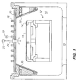
- FIG 1 shows an embodiment of the invention wherein the gas injector is centrally mounted in a plasma etch reactor such as the TCP 9100 TM made by LAM Research Corporation, the assignee of the present application.
- the etch reactor includes an antenna such as a planar coil mounted adjacent the exterior of a dielectric window and the substrate is supported on a chuck such as a cantilevered electrostatic chuck.
- the gas injector is mounted in an opening extending through the dielectric window.
- the vacuum processing chamber 10 includes a substrate holder 12 prcviding an electrostatic clamping force to a substrate 13 as well as an RF bias to a substrate supported thereon and a focus ring 14 for confining plasma in an area above the substrate while it is He backcooled.
- a source of energy for maintaining a high density (e.g. 10 11 -10 12 ions/cm 3 ) plasma in the chamber such as an antenna 18 powered by a suitable RF source and associated RF impedance matching circuitry 19 inductively couples RF energy into the chamber 10 so as to provide a high density plasma.
- the chamber includes suitable vacuum pumping apparatus connected to outlet 15 for maintaining the interior of the chamber at a desired pressure (e.g.
- a substantially planar dielectric window 20 of uniform thickness is provided between the antenna 18 and the interior of the processing chamber 10 and forms the vacuum wall at the top of the processing chamber 10.
- a gas injector 22 is provided in an opening in the window 20 and includes a plurality of gas outlets such as circular holes (not shown) for delivering process gas supplied by the gas supply 23 to the processing chamber 10.
- a conical liner 30 extends from the window 20 and surrounds the substrate holder 12.
- a semiconductor substrate such as a wafer is positioned on the substrate holder 12 and is typically held in place by an electrostatic clamp, a mechanical clamp, or other clamping mechanism when He backcooling is employed.
- Process gas is then supplied to the vacuum processing chamber 10 by passing the process gas through the gas injector 22.
- the window 20 can be planar and of uniform thickness as shown in Figure 1 or have other configurations such as non-planar and/or non-uniform thickness geometries.
- a high density plasma is ignited in the space between the substrate and the window by supplying suitable RF power to the antenna 18. After completion of etching of an individual substrate, the processed substrate is removed from the chamber and another substrate is transferred into the chamber for processing thereof.
- the gas injector 22 can comprise a separate member of the same or different material as the window.
- the gas injector can be made of metal such as aluminum or stainless steel or dielectric materials such as quartz, alumina, silicon nitride, etc.
- the gas injector is removably mounted in an opening in the window.
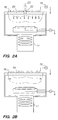
- Figures 2a and 2b show gas distribution effects of different gas supply arrangements in an inductively coupled plasma reactor having a vacuum pump 17 connected to an outlet in the bottom of the processing chamber.
- the plasma reactor includes a gas injector in accordance with the present invention whereas the Figure 2b arrangement includes a gas ring arrangement.
- the gas injector is mounted in an opening in the window such that a lower end of the gas injector is flush with the inner surface of the window.
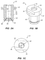
- Figures 3a-c show details of a gas injector design in accordance with the invention.
- the gas injector 22 includes a cylindrical body 40 having a flange 42 at an upper end thereof, a central bore 44 extending through the upper axial end, a plurality of gas outlets 46 extending between the bore and the exterior surface of the lower axial end, and O-ring grooves 48, 50.
- the upper axial end of the gas injector includes a pair of flat surfaces 54, 56 on opposite sides thereof.
- four gas outlets 46 open into the lower end of the bore 44 and the gas outlets 46 are spaced apart by 90°.
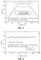
- Figure 4 is a graph of local SiCl x emission from a 300 mm LAM TCP TM plasma reactor fitted with a gas injector providing top gas injection according to the present invention compared to the same reactor fitted with a gas ring providing side gas injection.
- the reactor was operated at 10 mTorr (33 Pa) reactor pressure, 800 watts power to the RF antenna, 150 watts power to the bottom electrode in the ESC, 100 sccm Cl 2 and 100 sccm Ar.
- the intensity of etch by-product distribution above the exposed surface of a 300 mm wafer is substantially more uniform with top gas injection.
- Figure 5 is a graph of chlorine atom distribution from a 300 mm LAM TCP TM plasma reactor fitted with a gas injector providing top gas injection according to the present invention.
- the reactor was operated at 10 mTorr (1.33 Pa) reactor pressure, 800 watts power to the RF antenna, 150 watts power to the bottom electrode in the ESC, 100 sccm Cl 2 and 100 sccm Ar.
- the intensity of chlorine atom distribution above the exposed surface of the wafer is substantially uniform across a 300 mm wafer.
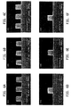
- Figures 6a-c are SEM (scanning electron microscope) images of etch profiles in polysilicon dense lines and Figures 6d-f are SEM (scanning electron microscope) images of etch profiles in polysilicon isolated lines.
- the etch profiles are obtained from a 300 mm wafer processed in a 300 mm reactor operated at 10 mTorr (1.33 Pa) and fitted with a top gas injector supplying 420 sccm total gas flow.
- Figure 6a shows the etch profile at the center of the wafer
- Figure 6b shows the etch profile at a location intermediate the center and edge of the wafer
- Figure 6c shows the etch profile at the edge of the wafer.
- Figure 6d shows the etch profile at the center of the wafer
- Figure 6e shows the etch profile at a location intermediate the center and edge of the wafer
- Figure 6f shows the etch profile at the edge of the wafer.
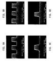
- Figures 7a-d are SEM (scanning electron microscope) images of etch profiles in polysilicon a ross a 300 mm wafer processed in a 300 mm reactor operated at 10 mTorr (1.33 Pa) reactor pressure and fitted with a top gas injector supplying 200 sccm total gas flow.
- Figure 7a shows the etch profile of dense lines at the center of the wafer and
- Figure 7b shows the etch profile of dense lines at the edge of the wafer.
- SEM images show that the etch profile is substantially uniform across the 300 mm wafer.
- Figures 7c and 7d show etch profiles of isolated lines at the center and edge of the wafer.
- the delta CD (the difference between the width at the top and bottom of the line) is 68.75 nm at the center and 56.25 nm at the edge, the difference in delta CD at the center and edge being 12.5 nm or 0.0125 ⁇ m.
- Figures 8a-d are SEM (scanning electron microscope) images of etch profiles in polysilicon across a 300 mm wafer processed in a 300 mm reactor operated at 10 mTorr (1.33 Pa) reactor pressure and fitted with side gas injection supplying 200 sccm total gas flow.
- Figure 8a shows the etch profile of dense lines at the center of the wafer and
- Figure 8b shows the etch profile of dense lines at the edge of the wafer.
- These SEM images show that the etch profile is not as uniform across the 300 mm wafer as in the case of top gas injection shown in Figures 7a-d .
- Figures 8c and 8d show etch profiles of an isolated line at the center and edge of the wafer.
- the delta CD is 112.5 nm at the center and 62.5 nm at the edge, the difference in delta CD at the center and edge being 50 nm or 0.05 ⁇ m.
- the gas injector is a cylindrical member having a diameter of 1 inch and either 8 or 9 gas outlets in one end thereof.
- the 9 gas outlet arrangement is useful for a polysilicon etching process and the 8 gas outlet arrangement is useful for an aluminum etching process.
- one hole is provided in the center of the axial end of the gas injector and 8 holes are spaced 45° apart and located adjacent the outer periphery of the axial end.
- the center hole is omitted.
- the 8 holes can extend axially or they can be at an angle to the central axis of the bore extending part way through the gas injector.
- a preferred angle is 10 to 75°, more preferably 10 to 45° with about 30° being the most desirable angle of injection when the axial end face of the injector is flush with the inner surface of the window.
- the mounting arrangement for the gas injector is a removable mounting arrangement.
- the gas injector could be screwed into the window or clamped to the window by a suitable clamping arrangement.
- the removable mounting arrangement is one in which the gas injector is simply slidably fitted in the window with only one or more O-rings between the window and gas injector.
- an O-ring can be provided in a groove around a lower part of the gas injector to provide a seal between the gas injector and the opening in the window.
- Another O-ring is provided in a groove in an upper part of the gas injector to provide a seal between the gas injector and an exterior surface of the window.
- the gas injector advantageously allows an operator to modify a process gas supply arrangement for a plasma etch reactor to optimize gas distribution in the reactor. For example, in plasma etching aluminum it is desirable to distribute the process gas into the plasma rather than direct the process gas directly towards the substrate being etched. In plasma etching polysilicon it is desirable to distribute the process gas into the plasma and direct the process gas directly towards the substrate being etched. Further optimization may involve selecting a gas injector which extends a desired distance below the inner surface of the window and/or includes a particular gas outlet arrangement.
- the number of gas outlets, the location of the gas outlets such as on the axial end and/or along the sides of the gas injector as well as the angle(s) of injection of the gas outlets can be selected to provide optimum etching results.
- the angle of injection is preferably larger for larger size substrates.
- the gas injector can be used to plasma etch aluminum by injecting the process gas into the interior of the chamber such that the gas is not injected directly towards the substrate being processed.
- the gas injector does not include a central gas outlet in the axial end thereof. Instead, 4 or 8 gas outlets located around the periphery of the axial end are used to inject the gas at an angle of 30 to 60°, preferably 30 to 45° with respect to a direction perpendicular to the exposed surface of the substrate.
- the process gas can include 100 to 500 sccm of a mixture of Cl 2 and BCl 3 or Cl 2 and N 2 or BCl 3 , Cl 2 and N 2 .
- the gas injector can also be used to plasma etch polysilicon by injecting the process gas into the interior of the chamber such that the gas is injected directly towards the substrate being processed.
- the gas injector includes a central gas outlet in the axial end thereof and 4 or 8 gas outlets located around the periphery of the axial end are used to inject the gas at an angle of 10 to 70°, preferably 30 to 60° with respect to a direction perpendicular to the exposed surface of the substrate.
- the process gas can include 100 to 500 sccm of a mixture of Cl 2 and HBr or Cl 2 only or HBr only.
- the most preferred location of the gas injector is in the center of the coil. Such a location avoids exposure of the gas injector to the toroidal zone of plasma formed by the coil.
- the gas outlets are located in a region of reduced electric field strength at which there is reduced plasma induced reactant decomposition. That is, there is less effect of the presence of a thin (e.g., ⁇ 1mm) plasma sheath surrounding the distal end of the gas injector which otherwise might cause electric field lines (created by the difference in potential between the plasma and grounded injector tubes) to be quite large and lead to locally enhanced deposition during etching or deposition which ultimately can clog outlets located in such regions.
- the gas injector is located beyond the enhanced electric field so as to reduce susceptibility to clogging, particularly during successive plasma processing of individual substrates such as semiconductor wafers.
- the substrate In processing a semiconductor substrate, the substrate is inserted into the processing chamber 140 and clamped by a mechanical or electrostatic clamp to a substrate support.
- the substrate is processed in the processing chamber by energizing a process gas in the processing chamber into a high density plasma.
- a source of energy maintains a high density (e.g., 10 9 -10 12 ions/cm 3 , preferably 10 10 -10 12 ions/cm 3 ) plasma in the chamber.
- an antenna 150 such as the planar multiturn spiral coil, a non-planar multiturn coil, or an antenna having another shape, powered by a suitable RF source and suitable RF impedance matching circuitry inductively couples RF energy into the chamber to generate a high density plasma.
- the chamber may include a suitable vacuum pumping apparatus for maintaining the interior of the chamber at a desired pressure (e.g., below 5 mTorr (666 Pa) preferably 1-100 mTorr (0.133-13.3 Pa).
- a dielectric window such as the planar dielectric window 155 of uniform thickness or a non-planar dielectric window is provided between the antenna 150 and the interior of the processing chamber 140 and forms the vacuum wall at the top of the processing chamber 140.
- a gas supply supplying process gas into the chamber includes the gas injector described above.
- the process gases include reactive gasses and optional carrier gases such as Ar. Due to the small orifice size and number of gas outlets, a large pressure differential can develop between the gas injector and the chamber interior. For example, with the gas injector at a pressure of > 1 Torr (0.133 Pa), and the chamber interior at a pressure of about 10 mTorr (1.33 Pa) the pressure differential is about 100:1. This results in choked, sonic flow at the gas outlets. If desired, the interior orifice of the gas outlets can be contoured to provide supersonic flow at the outlet.
- Injecting the process gas at sonic velocity inhibits the plasma from penetrating the gas outlets.
- deposition of materials such as doped or undoped silicon dioxide
- such a design prevents plasma-induced decomposition of gases such as SiH 4 and the subsequent formation of amorphous silicon residues within the gas outlets.
- the plasma processing system according to this embodiment provides an increased deposition rate and improved uniformity on the substrate, compared to conventional gas distribution systems, by concentrating the silicon-containing process gas above the substrate and by preferentially directing the process gas onto specific regions of the substrate.
- the plasma generated by exciting the process gas is an electrically conductive gas which floats at an elevated electrical potential, i.e., the plasma potential.
- the plasma potential is largely determined by the capacitive coupling between the plasma and the RF-driven substrate electrode. Under typical conditions, the plasma potential can reach hundreds of volts.
- the gas injector generally remains at a lower potential (e.g., ground potential for a metallic injector) than the plasma.
- a a thin sheath can form around a "plasma immersed" portion of the gas injector if the gas injector extends into the zone of plasma, in which case electric field lines created by the difference in potential between the plasma and the grounded gas injector would be perpendicular to the sheath.
- etch uniformity of metal such as aluminum, conductive semiconductor materials such as polysilicon and dielectric materials such as silicon dioxide including photoresist etch uniformity and selectivity to underlying materials using halogen and halocarbon based chemistries are improved.
- conventional injection through a showerhead incorporated in or below a dielectric window can result in nonuniform etching across the substrate, e.g., "center fast resist etching", which can lead to poor control of the etched features and profiles, and differences in features at the substrate center and edge.
- polymer formation on the TCPTM window or the showerhead can lead to undesirable particle flaking and contamination on the substrate.
- showerhead arrangements include the additional costs associated with providing a sandwich type structure for delivering gas across the window, temperature control, the effects of gas/plasma erosion of the showerhead, ignition of plasma in the showerhead gas outlets or gap between the showerhead and the overlying window, lack of process repeatability, process drift, etc.
- edge injection via a gas injection ring can result in "edge fast etching" and polymer deposition on the chamber walls.
- Photoresist to oxide selectivities are typically only 1-4 in these cases, where 5-10 would be desirable.
- the gas injector according to the invention can provide improvement in the uniformity of the resist etch rate (typically 6% 3 ⁇ ) with simultaneous resist to oxide selectivities of 5, preferably 10 or more.
- the present preferred injection design thus appears to provide a much more uniform flux of reactive intermediates and chemical radicals to the substrate surface, including both etch species, such as atomic chlorine and fluorine, and polymerizing species, such as CF, CF 2 , and CF 3 .
- process gas is injected within the plasma region facing and in close proximity to, the center of the substrate.
- gas outlets of the gas injector can be located far enough below the inner surface of the window such that the gas outlets are immersed within the plasma.
- the gas outlets are preferably located such that there is adequate diffusion of the ions and neutral species in order to ensure a uniform etch or deposition rate.
- the gas injector can be located in a region where the azimuthal electric field induced by the TCPTM coil falls to zero, which minimizes perturbations of the plasma generation zone.
- the gas injector is immersed a suitable distance such as no more than about 80% of the distance between the chamber ceiling and the substrate. This ensures that the ion diffusion from upper regions of the chamber have sufficient space to fill in the lower ion density immediately beneath the gas injector. This will minimize any "shadow" of the gas injector in the ion flux to the substrate.
- the immersed gas injector allows for independent selection of the center gas feed location and the chamber aspect ratio. This facilitates efficient utilization of process gas and improves process gas delivery to the central region of large area substrates with minimal disturbance to plasma uniformity. This configuration is also advantageous because locating the gas outlets close to the substrate increases the convective transport relative to diffusive transport in the region immediately above the substrate.
- the gas injector facilitates efficient transport of etch by-products out of the substrate region, which can favorably impact etch uniformity and profile control, particularly in chemically driven applications such as aluminum etching.
- the injection orifices are small enough that any plasma sheath formed around the gas injector is largely unaffected by the presence of the gas outlets.
- the total area of the gas outlets can be less than, greater than or the same as the cross-sectional area of the bore in the gas injector.
- the total area of the gas outlets preferably ensures that process gas be delivered from each gas outlet so as to be distributed evenly within the chamber.
- the injection to various regions above the substrate can be tailored by utilizing the same or different diameters for the various gas outlets.
- the gas outlets can have any desired shape such as uniform diameter along the entire length thereof or other shape such as conically tapered, flared surfaces or radially contoured surfaces.
- the gas outlets can be oriented to inject the gas in any direction, including directly at the substrate, at an acute angle with respect to the substrate, parallel to the substrate or back toward the upper plasma boundary surface (at an oblique angle with respect to the longitudinal axis of the nozzle), or combinations thereof. It is desired to achieve a uniform flux of chemical radicals and reactive intermediate species onto the substrate surface to facilitate uniform etch and deposition rates across the large area substrate. If desired, additional gas injection arrangements can also be provided near the periphery of the substrate or from other chamber walls.
Landscapes
- Physics & Mathematics (AREA)
- Engineering & Computer Science (AREA)
- Plasma & Fusion (AREA)
- Chemical & Material Sciences (AREA)
- Analytical Chemistry (AREA)
- Drying Of Semiconductors (AREA)
- Chemical Vapour Deposition (AREA)
- Physical Or Chemical Processes And Apparatus (AREA)
Applications Claiming Priority (3)
| Application Number | Priority Date | Filing Date | Title |
|---|---|---|---|
| US223273 | 1998-12-30 | ||
| US09/223,273 US6230651B1 (en) | 1998-12-30 | 1998-12-30 | Gas injection system for plasma processing |
| PCT/US1999/027917 WO2000041212A1 (en) | 1998-12-30 | 1999-12-07 | Gas injection system for plasma processing |
Publications (2)
| Publication Number | Publication Date |
|---|---|
| EP1145277A1 EP1145277A1 (en) | 2001-10-17 |
| EP1145277B1 true EP1145277B1 (en) | 2012-02-08 |
Family
ID=22835796
Family Applications (1)
| Application Number | Title | Priority Date | Filing Date |
|---|---|---|---|
| EP99967134A Expired - Lifetime EP1145277B1 (en) | 1998-12-30 | 1999-12-07 | Gas injection system for plasma processing |
Country Status (7)
| Country | Link |
|---|---|
| US (3) | US6230651B1 (enExample) |
| EP (1) | EP1145277B1 (enExample) |
| JP (1) | JP4588885B2 (enExample) |
| KR (1) | KR100665646B1 (enExample) |
| IL (1) | IL144001A (enExample) |
| TW (1) | TW548680B (enExample) |
| WO (1) | WO2000041212A1 (enExample) |
Families Citing this family (114)
| Publication number | Priority date | Publication date | Assignee | Title |
|---|---|---|---|---|
| US6129808A (en) * | 1998-03-31 | 2000-10-10 | Lam Research Corporation | Low contamination high density plasma etch chambers and methods for making the same |
| US6230651B1 (en) * | 1998-12-30 | 2001-05-15 | Lam Research Corporation | Gas injection system for plasma processing |
| US6432259B1 (en) * | 1999-12-14 | 2002-08-13 | Applied Materials, Inc. | Plasma reactor cooled ceiling with an array of thermally isolated plasma heated mini-gas distribution plates |
| US6451161B1 (en) * | 2000-04-10 | 2002-09-17 | Nano-Architect Research Corporation | Method and apparatus for generating high-density uniform plasma |
| US6716302B2 (en) | 2000-11-01 | 2004-04-06 | Applied Materials Inc. | Dielectric etch chamber with expanded process window |
| US6403491B1 (en) * | 2000-11-01 | 2002-06-11 | Applied Materials, Inc. | Etch method using a dielectric etch chamber with expanded process window |
| KR100413145B1 (ko) * | 2001-01-11 | 2003-12-31 | 삼성전자주식회사 | 가스 인젝터 및 이를 갖는 식각 장치 |
| US6852167B2 (en) * | 2001-03-01 | 2005-02-08 | Micron Technology, Inc. | Methods, systems, and apparatus for uniform chemical-vapor depositions |
| US6758909B2 (en) * | 2001-06-05 | 2004-07-06 | Honeywell International Inc. | Gas port sealing for CVD/CVI furnace hearth plates |
| US6548416B2 (en) * | 2001-07-24 | 2003-04-15 | Axcelis Technolgoies, Inc. | Plasma ashing process |
| EP1421606A4 (en) * | 2001-08-06 | 2008-03-05 | Genitech Co Ltd | PLASMA ACTIVE ATOMIC LAYER (PEALD) DEPOSITION APPARATUS AND METHOD OF FORMING THIN FILM USING SAID APPARATUS |
| US20030070620A1 (en) * | 2001-10-15 | 2003-04-17 | Cooperberg David J. | Tunable multi-zone gas injection system |
| US7160577B2 (en) | 2002-05-02 | 2007-01-09 | Micron Technology, Inc. | Methods for atomic-layer deposition of aluminum oxides in integrated circuits |
| JP4338355B2 (ja) * | 2002-05-10 | 2009-10-07 | 東京エレクトロン株式会社 | プラズマ処理装置 |
| WO2003100817A1 (en) * | 2002-05-23 | 2003-12-04 | Lam Research Corporation | Multi-part electrode for a semiconductor processing plasma reactor and method of replacing a portion of a mutli-part electrode |
| WO2004015165A1 (en) * | 2002-08-08 | 2004-02-19 | Trikon Technologies Limited | Improvements to showerheads |
| US7270713B2 (en) * | 2003-01-07 | 2007-09-18 | Applied Materials, Inc. | Tunable gas distribution plate assembly |
| WO2004088729A1 (en) * | 2003-03-26 | 2004-10-14 | Tokyo Electron Limited | Chemical processing system and method |
| US6942753B2 (en) * | 2003-04-16 | 2005-09-13 | Applied Materials, Inc. | Gas distribution plate assembly for large area plasma enhanced chemical vapor deposition |
| EP1629522A4 (en) * | 2003-05-30 | 2008-07-23 | Aviza Tech Inc | GAS DISTRIBUTION SYSTEM |
| US7083903B2 (en) * | 2003-06-17 | 2006-08-01 | Lam Research Corporation | Methods of etching photoresist on substrates |
| JP2005072446A (ja) * | 2003-08-27 | 2005-03-17 | Chi Mei Electronics Corp | プラズマ処理装置及び基板の表面処理装置 |
| KR100859265B1 (ko) * | 2003-12-30 | 2008-09-18 | 동부일렉트로닉스 주식회사 | 반도체 제조 설비의 공정 가스 유입관 구조 |
| KR101025323B1 (ko) * | 2004-01-13 | 2011-03-29 | 가부시키가이샤 아루박 | 에칭 장치 및 에칭 방법 |
| US7708859B2 (en) * | 2004-04-30 | 2010-05-04 | Lam Research Corporation | Gas distribution system having fast gas switching capabilities |
| US20070066038A1 (en) | 2004-04-30 | 2007-03-22 | Lam Research Corporation | Fast gas switching plasma processing apparatus |
| US20060021703A1 (en) * | 2004-07-29 | 2006-02-02 | Applied Materials, Inc. | Dual gas faceplate for a showerhead in a semiconductor wafer processing system |
| US7081421B2 (en) | 2004-08-26 | 2006-07-25 | Micron Technology, Inc. | Lanthanide oxide dielectric layer |
| US7494939B2 (en) | 2004-08-31 | 2009-02-24 | Micron Technology, Inc. | Methods for forming a lanthanum-metal oxide dielectric layer |
| US20060051965A1 (en) * | 2004-09-07 | 2006-03-09 | Lam Research Corporation | Methods of etching photoresist on substrates |
| US7235501B2 (en) | 2004-12-13 | 2007-06-26 | Micron Technology, Inc. | Lanthanum hafnium oxide dielectrics |
| KR20060076346A (ko) * | 2004-12-29 | 2006-07-04 | 주식회사 하이닉스반도체 | 반도체 제조용 고밀도 플라즈마 화학기상증착 장치 |
| JP3984638B2 (ja) * | 2005-03-30 | 2007-10-03 | 松下電器産業株式会社 | 伝送線路対及び伝送線路群 |
| US7662729B2 (en) | 2005-04-28 | 2010-02-16 | Micron Technology, Inc. | Atomic layer deposition of a ruthenium layer to a lanthanide oxide dielectric layer |
| KR100522166B1 (ko) * | 2005-05-26 | 2005-10-18 | 한국기계연구원 | 플라즈마 반응장치 |
| US7927948B2 (en) | 2005-07-20 | 2011-04-19 | Micron Technology, Inc. | Devices with nanocrystals and methods of formation |
| US20070032081A1 (en) * | 2005-08-08 | 2007-02-08 | Jeremy Chang | Edge ring assembly with dielectric spacer ring |
| JP4628900B2 (ja) * | 2005-08-24 | 2011-02-09 | 株式会社日立ハイテクノロジーズ | プラズマ処理装置 |
| US7703479B2 (en) * | 2005-10-17 | 2010-04-27 | The University Of Kentucky Research Foundation | Plasma actuator |
| US20090087967A1 (en) * | 2005-11-14 | 2009-04-02 | Todd Michael A | Precursors and processes for low temperature selective epitaxial growth |
| KR100707983B1 (ko) * | 2005-11-28 | 2007-04-16 | 주식회사 에이이티 | 산화막의 원자층 에칭방법 |
| US7679024B2 (en) * | 2005-12-23 | 2010-03-16 | Lam Research Corporation | Highly efficient gas distribution arrangement for plasma tube of a plasma processing chamber |
| US7554053B2 (en) * | 2005-12-23 | 2009-06-30 | Lam Research Corporation | Corrugated plasma trap arrangement for creating a highly efficient downstream microwave plasma system |
| US7562638B2 (en) * | 2005-12-23 | 2009-07-21 | Lam Research Corporation | Methods and arrangement for implementing highly efficient plasma traps |
| US8088248B2 (en) | 2006-01-11 | 2012-01-03 | Lam Research Corporation | Gas switching section including valves having different flow coefficients for gas distribution system |
| US7685965B1 (en) * | 2006-01-26 | 2010-03-30 | Lam Research Corporation | Apparatus for shielding process chamber port |
| JP4833778B2 (ja) * | 2006-02-13 | 2011-12-07 | 東京エレクトロン株式会社 | 基板処理装置及び基板処理方法 |
| JP4674177B2 (ja) * | 2006-03-15 | 2011-04-20 | 株式会社日立ハイテクノロジーズ | プラズマ処理装置 |
| US20070249173A1 (en) * | 2006-04-21 | 2007-10-25 | Applied Materials, Inc. | Plasma etch process using etch uniformity control by using compositionally independent gas feed |
| US8187415B2 (en) * | 2006-04-21 | 2012-05-29 | Applied Materials, Inc. | Plasma etch reactor with distribution of etch gases across a wafer surface and a polymer oxidizing gas in an independently fed center gas zone |
| US20070254483A1 (en) * | 2006-04-28 | 2007-11-01 | Applied Materials, Inc. | Plasma etch process using polymerizing etch gases and an inert diluent gas in independent gas injection zones to improve etch profile or etch rate uniformity |
| US7541292B2 (en) * | 2006-04-28 | 2009-06-02 | Applied Materials, Inc. | Plasma etch process with separately fed carbon-lean and carbon-rich polymerizing etch gases in independent inner and outer gas injection zones |
| US7540971B2 (en) * | 2006-04-28 | 2009-06-02 | Applied Materials, Inc. | Plasma etch process using polymerizing etch gases across a wafer surface and additional polymer managing or controlling gases in independently fed gas zones with time and spatial modulation of gas content |
| US7431859B2 (en) * | 2006-04-28 | 2008-10-07 | Applied Materials, Inc. | Plasma etch process using polymerizing etch gases with different etch and polymer-deposition rates in different radial gas injection zones with time modulation |
| US8231799B2 (en) * | 2006-04-28 | 2012-07-31 | Applied Materials, Inc. | Plasma reactor apparatus with multiple gas injection zones having time-changing separate configurable gas compositions for each zone |
| US8747555B2 (en) * | 2006-05-09 | 2014-06-10 | Ulvac, Inc. | Thin film production apparatus and inner block for thin film production apparatus |
| US7605063B2 (en) * | 2006-05-10 | 2009-10-20 | Lam Research Corporation | Photoresist stripping chamber and methods of etching photoresist on substrates |
| KR100748872B1 (ko) * | 2006-06-09 | 2007-08-13 | 에이피티씨 주식회사 | 가스 공급 인젝터를 포함하는 플라즈마 공정 장비 |
| US7928366B2 (en) * | 2006-10-06 | 2011-04-19 | Lam Research Corporation | Methods of and apparatus for accessing a process chamber using a dual zone gas injector with improved optical access |
| WO2008005540A2 (en) * | 2006-07-07 | 2008-01-10 | Accretech Usa, Inc. | Method and apparatus for cleaning a wafer substrate |
| US7972471B2 (en) * | 2007-06-29 | 2011-07-05 | Lam Research Corporation | Inductively coupled dual zone processing chamber with single planar antenna |
| KR20090018290A (ko) * | 2007-08-17 | 2009-02-20 | 에이에스엠지니텍코리아 주식회사 | 증착 장치 |
| US20090221149A1 (en) * | 2008-02-28 | 2009-09-03 | Hammond Iv Edward P | Multiple port gas injection system utilized in a semiconductor processing system |
| JP5223377B2 (ja) | 2008-02-29 | 2013-06-26 | 東京エレクトロン株式会社 | プラズマ処理装置用の電極、プラズマ処理装置及びプラズマ処理方法 |
| JP5230225B2 (ja) * | 2008-03-06 | 2013-07-10 | 東京エレクトロン株式会社 | 蓋部品、処理ガス拡散供給装置、及び基板処理装置 |
| KR101624123B1 (ko) * | 2008-10-31 | 2016-05-25 | 램 리써치 코포레이션 | 플라즈마 프로세싱 챔버의 하부 전극 어셈블리 |
| KR200475462Y1 (ko) * | 2009-03-27 | 2014-12-03 | 램 리써치 코포레이션 | 플라즈마 처리 장치의 교체 가능한 상부 챔버 섹션 |
| US8415884B2 (en) * | 2009-09-08 | 2013-04-09 | Tokyo Electron Limited | Stable surface wave plasma source |
| MY165356A (en) | 2009-09-10 | 2018-03-21 | Lam Res Corp | Replaceable upper chamber parts of plasma processing apparatus |
| JP5808750B2 (ja) * | 2009-11-30 | 2015-11-10 | ラム リサーチ コーポレーションLam Research Corporation | 傾斜側壁を備える静電チャック |
| DE202010015933U1 (de) | 2009-12-01 | 2011-03-31 | Lam Research Corp.(N.D.Ges.D.Staates Delaware), Fremont | Eine Randringanordnung für Plasmaätzkammern |
| US20110278260A1 (en) * | 2010-05-14 | 2011-11-17 | Applied Materials, Inc. | Inductive plasma source with metallic shower head using b-field concentrator |
| US9171702B2 (en) | 2010-06-30 | 2015-10-27 | Lam Research Corporation | Consumable isolation ring for movable substrate support assembly of a plasma processing chamber |
| US8826855B2 (en) | 2010-06-30 | 2014-09-09 | Lam Research Corporation | C-shaped confinement ring for a plasma processing chamber |
| US8485128B2 (en) | 2010-06-30 | 2013-07-16 | Lam Research Corporation | Movable ground ring for a plasma processing chamber |
| US9728429B2 (en) | 2010-07-27 | 2017-08-08 | Lam Research Corporation | Parasitic plasma prevention in plasma processing chambers |
| US10658161B2 (en) * | 2010-10-15 | 2020-05-19 | Applied Materials, Inc. | Method and apparatus for reducing particle defects in plasma etch chambers |
| US8133349B1 (en) | 2010-11-03 | 2012-03-13 | Lam Research Corporation | Rapid and uniform gas switching for a plasma etch process |
| US8288174B1 (en) | 2011-03-24 | 2012-10-16 | Tokyo Electron Limited | Electrostatic post exposure bake apparatus and method |
| US8562785B2 (en) | 2011-05-31 | 2013-10-22 | Lam Research Corporation | Gas distribution showerhead for inductively coupled plasma etch reactor |
| US9245717B2 (en) | 2011-05-31 | 2016-01-26 | Lam Research Corporation | Gas distribution system for ceramic showerhead of plasma etch reactor |
| US9947512B2 (en) * | 2011-10-25 | 2018-04-17 | Lam Research Corporation | Window and mounting arrangement for twist-and-lock gas injector assembly of inductively coupled plasma chamber |
| US9679751B2 (en) | 2012-03-15 | 2017-06-13 | Lam Research Corporation | Chamber filler kit for plasma etch chamber useful for fast gas switching |
| US10174422B2 (en) | 2012-10-25 | 2019-01-08 | Applied Materials, Inc. | Apparatus for selective gas injection and extraction |
| US9790596B1 (en) * | 2013-01-30 | 2017-10-17 | Kyocera Corporation | Gas nozzle and plasma device employing same |
| US9314854B2 (en) | 2013-01-30 | 2016-04-19 | Lam Research Corporation | Ductile mode drilling methods for brittle components of plasma processing apparatuses |
| US8893702B2 (en) | 2013-02-20 | 2014-11-25 | Lam Research Corporation | Ductile mode machining methods for hard and brittle components of plasma processing apparatuses |
| US9536710B2 (en) | 2013-02-25 | 2017-01-03 | Applied Materials, Inc. | Tunable gas delivery assembly with internal diffuser and angular injection |
| KR102176189B1 (ko) | 2013-03-12 | 2020-11-09 | 어플라이드 머티어리얼스, 인코포레이티드 | 방위각 및 방사상 분배 제어되는 다중-구역 가스 주입 조립체 |
| US10163606B2 (en) | 2013-03-15 | 2018-12-25 | Applied Materials, Inc. | Plasma reactor with highly symmetrical four-fold gas injection |
| US9449797B2 (en) | 2013-05-07 | 2016-09-20 | Lam Research Corporation | Component of a plasma processing apparatus having a protective in situ formed layer on a plasma exposed surface |
| US9275869B2 (en) * | 2013-08-02 | 2016-03-01 | Lam Research Corporation | Fast-gas switching for etching |
| US9123661B2 (en) | 2013-08-07 | 2015-09-01 | Lam Research Corporation | Silicon containing confinement ring for plasma processing apparatus and method of forming thereof |
| US10553398B2 (en) * | 2013-09-06 | 2020-02-04 | Applied Materials, Inc. | Power deposition control in inductively coupled plasma (ICP) reactors |
| US10249511B2 (en) * | 2014-06-27 | 2019-04-02 | Lam Research Corporation | Ceramic showerhead including central gas injector for tunable convective-diffusive gas flow in semiconductor substrate processing apparatus |
| JP6499835B2 (ja) * | 2014-07-24 | 2019-04-10 | 株式会社日立ハイテクノロジーズ | プラズマ処理装置およびプラズマ処理方法 |
| US10465288B2 (en) * | 2014-08-15 | 2019-11-05 | Applied Materials, Inc. | Nozzle for uniform plasma processing |
| US9966270B2 (en) * | 2015-03-31 | 2018-05-08 | Lam Research Corporation | Gas reaction trajectory control through tunable plasma dissociation for wafer by-product distribution and etch feature profile uniformity |
| KR101633721B1 (ko) * | 2015-11-27 | 2016-06-27 | (주)이엠아이티 | 수직 다중 기둥 구조를 갖는 rf 안테나 |
| US9716005B1 (en) | 2016-03-18 | 2017-07-25 | Applied Materials, Inc. | Plasma poisoning to enable selective deposition |
| KR102553629B1 (ko) * | 2016-06-17 | 2023-07-11 | 삼성전자주식회사 | 플라즈마 처리 장치 |
| US20190032211A1 (en) * | 2017-07-28 | 2019-01-31 | Lam Research Corporation | Monolithic ceramic gas distribution plate |
| US11670490B2 (en) * | 2017-09-29 | 2023-06-06 | Taiwan Semiconductor Manufacturing Co., Ltd. | Integrated circuit fabrication system with adjustable gas injector |
| US10840066B2 (en) * | 2018-06-13 | 2020-11-17 | Taiwan Semiconductor Manufacturing Co., Ltd. | Adjustable fastening device for plasma gas injectors |
| CN110223904A (zh) * | 2019-07-19 | 2019-09-10 | 江苏鲁汶仪器有限公司 | 一种具有法拉第屏蔽装置的等离子体处理系统 |
| CN111081525B (zh) * | 2019-12-31 | 2021-06-08 | 江苏鲁汶仪器有限公司 | 一种阻挡工艺腔室等离子体反流保护进气结构的装置 |
| CN115362538A (zh) * | 2020-04-06 | 2022-11-18 | 朗姆研究公司 | 气体注射器的陶瓷增材制造技术 |
| CN113707527B (zh) * | 2020-05-21 | 2022-07-29 | 江苏鲁汶仪器有限公司 | 一种阻挡等离子体反流的分离式进气结构 |
| TWI767244B (zh) * | 2020-05-29 | 2022-06-11 | 朗曦科技股份有限公司 | 半導體製程腔體之氣體噴頭 |
| KR20220021206A (ko) * | 2020-08-13 | 2022-02-22 | 삼성전자주식회사 | 플라즈마 처리 장치 |
| US20230317423A1 (en) * | 2020-10-30 | 2023-10-05 | Lam Research Corporation | Magnesium aluminum oxynitride component for use in a plasma processing chamber |
| JP7543176B2 (ja) * | 2021-03-08 | 2024-09-02 | 株式会社アルバック | プラズマ処理装置およびそのメンテナンス方法 |
| JP7791677B2 (ja) * | 2021-09-16 | 2025-12-24 | 株式会社Screenホールディングス | 基板処理装置および基板処理方法 |
| KR102887338B1 (ko) * | 2022-06-22 | 2025-11-14 | 나이스 스타 코퍼레이션 | 스월 모션 사이드 가스 피드가 구비된 플라즈마 챔버 |
Family Cites Families (66)
| Publication number | Priority date | Publication date | Assignee | Title |
|---|---|---|---|---|
| JPS51144183A (en) | 1975-06-06 | 1976-12-10 | Hitachi Ltd | Semiconductor element containing surface protection film |
| DE2608417C3 (de) * | 1976-03-01 | 1981-02-12 | Degussa Ag, 6000 Frankfurt | Verfahren und vorrichtung zur herstellung von russ |
| US4270999A (en) | 1979-09-28 | 1981-06-02 | International Business Machines Corporation | Method and apparatus for gas feed control in a dry etching process |
| JPS59150417A (ja) | 1983-02-08 | 1984-08-28 | Toshiba Corp | 気相成長方法およびその装置 |
| US4691662A (en) | 1983-02-28 | 1987-09-08 | Michigan State University | Dual plasma microwave apparatus and method for treating a surface |
| JPS6077429A (ja) * | 1983-10-04 | 1985-05-02 | Asahi Glass Co Ltd | ドライエツチング方法 |
| JPS61100935A (ja) | 1984-10-23 | 1986-05-19 | Fujitsu Ltd | ドライエツチング装置 |
| US4614639A (en) | 1985-04-26 | 1986-09-30 | Tegal Corporation | Compound flow plasma reactor |
| US4612077A (en) * | 1985-07-29 | 1986-09-16 | The Perkin-Elmer Corporation | Electrode for plasma etching system |
| US5160543A (en) | 1985-12-20 | 1992-11-03 | Canon Kabushiki Kaisha | Device for forming a deposited film |
| DE3885833T2 (de) | 1987-09-22 | 1994-03-24 | Nippon Electric Co | Chemischer Dampfabscheidungsapparat für die Herstellung von hochqualitativen epitaktischen Schichten mit gleichmässiger Dichte. |
| US4980204A (en) | 1987-11-27 | 1990-12-25 | Fujitsu Limited | Metal organic chemical vapor deposition method with controlled gas flow rate |
| US4996077A (en) | 1988-10-07 | 1991-02-26 | Texas Instruments Incorporated | Distributed ECR remote plasma processing and apparatus |
| US4943345A (en) | 1989-03-23 | 1990-07-24 | Board Of Trustees Operating Michigan State University | Plasma reactor apparatus and method for treating a substrate |
| US5104634A (en) * | 1989-04-20 | 1992-04-14 | Hercules Incorporated | Process for forming diamond coating using a silent discharge plasma jet process |
| US5134965A (en) | 1989-06-16 | 1992-08-04 | Hitachi, Ltd. | Processing apparatus and method for plasma processing |
| US5164040A (en) | 1989-08-21 | 1992-11-17 | Martin Marietta Energy Systems, Inc. | Method and apparatus for rapidly growing films on substrates using pulsed supersonic jets |
| JPH04355917A (ja) * | 1990-10-12 | 1992-12-09 | Seiko Epson Corp | 半導体装置の製造装置 |
| US5252132A (en) * | 1990-11-22 | 1993-10-12 | Mitsubishi Denki Kabushiki Kaisha | Apparatus for producing semiconductor film |
| JP2839720B2 (ja) | 1990-12-19 | 1998-12-16 | 株式会社東芝 | 熱処理装置 |
| US5531834A (en) | 1993-07-13 | 1996-07-02 | Tokyo Electron Kabushiki Kaisha | Plasma film forming method and apparatus and plasma processing apparatus |
| US5614055A (en) | 1993-08-27 | 1997-03-25 | Applied Materials, Inc. | High density plasma CVD and etching reactor |
| US5529657A (en) * | 1993-10-04 | 1996-06-25 | Tokyo Electron Limited | Plasma processing apparatus |
| TW293983B (enExample) | 1993-12-17 | 1996-12-21 | Tokyo Electron Co Ltd | |
| US5680013A (en) * | 1994-03-15 | 1997-10-21 | Applied Materials, Inc. | Ceramic protection for heated metal surfaces of plasma processing chamber exposed to chemically aggressive gaseous environment therein and method of protecting such heated metal surfaces |
| US5589002A (en) * | 1994-03-24 | 1996-12-31 | Applied Materials, Inc. | Gas distribution plate for semiconductor wafer processing apparatus with means for inhibiting arcing |
| US5522934A (en) | 1994-04-26 | 1996-06-04 | Tokyo Electron Limited | Plasma processing apparatus using vertical gas inlets one on top of another |
| US5425810A (en) * | 1994-05-11 | 1995-06-20 | Internation Business Machines Corporation | Removable gas injectors for use in chemical vapor deposition of aluminium oxide |
| US5426810A (en) * | 1994-05-23 | 1995-06-27 | Americo | Abrasive pad holder |
| GB9410567D0 (en) | 1994-05-26 | 1994-07-13 | Philips Electronics Uk Ltd | Plasma treatment and apparatus in electronic device manufacture |
| US5540800A (en) | 1994-06-23 | 1996-07-30 | Applied Materials, Inc. | Inductively coupled high density plasma reactor for plasma assisted materials processing |
| US5580385A (en) | 1994-06-30 | 1996-12-03 | Texas Instruments, Incorporated | Structure and method for incorporating an inductively coupled plasma source in a plasma processing chamber |
| US5643394A (en) * | 1994-09-16 | 1997-07-01 | Applied Materials, Inc. | Gas injection slit nozzle for a plasma process reactor |
| US5746875A (en) * | 1994-09-16 | 1998-05-05 | Applied Materials, Inc. | Gas injection slit nozzle for a plasma process reactor |
| JP3699142B2 (ja) | 1994-09-30 | 2005-09-28 | アネルバ株式会社 | 薄膜形成装置 |
| TW285746B (enExample) * | 1994-10-26 | 1996-09-11 | Matsushita Electric Industrial Co Ltd | |
| DE4440323A1 (de) * | 1994-11-11 | 1996-05-15 | Sulzer Metco Ag | Düse für einen Brennerkopf eines Plasmaspritzgeräts |
| JPH08158072A (ja) | 1994-12-02 | 1996-06-18 | Nippon Soken Inc | ドライエッチング装置 |
| US5685942A (en) * | 1994-12-05 | 1997-11-11 | Tokyo Electron Limited | Plasma processing apparatus and method |
| JPH0945624A (ja) | 1995-07-27 | 1997-02-14 | Tokyo Electron Ltd | 枚葉式の熱処理装置 |
| JP3150056B2 (ja) * | 1995-10-19 | 2001-03-26 | 東京エレクトロン株式会社 | プラズマ処理装置 |
| US5792269A (en) * | 1995-10-31 | 1998-08-11 | Applied Materials, Inc. | Gas distribution for CVD systems |
| US5772771A (en) | 1995-12-13 | 1998-06-30 | Applied Materials, Inc. | Deposition chamber for improved deposition thickness uniformity |
| US6070551A (en) * | 1996-05-13 | 2000-06-06 | Applied Materials, Inc. | Deposition chamber and method for depositing low dielectric constant films |
| US6013155A (en) * | 1996-06-28 | 2000-01-11 | Lam Research Corporation | Gas injection system for plasma processing |
| US5885358A (en) | 1996-07-09 | 1999-03-23 | Applied Materials, Inc. | Gas injection slit nozzle for a plasma process reactor |
| US6170428B1 (en) * | 1996-07-15 | 2001-01-09 | Applied Materials, Inc. | Symmetric tunable inductively coupled HDP-CVD reactor |
| US6090210A (en) | 1996-07-24 | 2000-07-18 | Applied Materials, Inc. | Multi-zone gas flow control in a process chamber |
| JP3220394B2 (ja) * | 1996-09-27 | 2001-10-22 | 東京エレクトロン株式会社 | プラズマ処理装置 |
| TW415970B (en) * | 1997-01-08 | 2000-12-21 | Ebara Corp | Vapor-phase film growth apparatus and gas ejection head |
| US6077357A (en) * | 1997-05-29 | 2000-06-20 | Applied Materials, Inc. | Orientless wafer processing on an electrostatic chuck |
| US6042687A (en) | 1997-06-30 | 2000-03-28 | Lam Research Corporation | Method and apparatus for improving etch and deposition uniformity in plasma semiconductor processing |
| TW416100B (en) | 1997-07-02 | 2000-12-21 | Applied Materials Inc | Control of oxygen to silane ratio in a seasoning process to improve particle performance in an HDP-CVD system |
| US6007330A (en) | 1998-03-12 | 1999-12-28 | Cosmos Factory, Inc. | Liquid precursor delivery system |
| US6194038B1 (en) | 1998-03-20 | 2001-02-27 | Applied Materials, Inc. | Method for deposition of a conformal layer on a substrate |
| US6294466B1 (en) | 1998-05-01 | 2001-09-25 | Applied Materials, Inc. | HDP-CVD apparatus and process for depositing titanium films for semiconductor devices |
| US6143078A (en) | 1998-11-13 | 2000-11-07 | Applied Materials, Inc. | Gas distribution system for a CVD processing chamber |
| US6230651B1 (en) * | 1998-12-30 | 2001-05-15 | Lam Research Corporation | Gas injection system for plasma processing |
| US6263829B1 (en) | 1999-01-22 | 2001-07-24 | Applied Materials, Inc. | Process chamber having improved gas distributor and method of manufacture |
| US6052176A (en) | 1999-03-31 | 2000-04-18 | Lam Research Corporation | Processing chamber with optical window cleaned using process gas |
| US6257168B1 (en) * | 1999-06-30 | 2001-07-10 | Lam Research Corporation | Elevated stationary uniformity ring design |
| US6287643B1 (en) | 1999-09-30 | 2001-09-11 | Novellus Systems, Inc. | Apparatus and method for injecting and modifying gas concentration of a meta-stable or atomic species in a downstream plasma reactor |
| US20030155079A1 (en) | 1999-11-15 | 2003-08-21 | Andrew D. Bailey | Plasma processing system with dynamic gas distribution control |
| US6486069B1 (en) * | 1999-12-03 | 2002-11-26 | Tegal Corporation | Cobalt silicide etch process and apparatus |
| US6450117B1 (en) | 2000-08-07 | 2002-09-17 | Applied Materials, Inc. | Directing a flow of gas in a substrate processing chamber |
| US6403491B1 (en) * | 2000-11-01 | 2002-06-11 | Applied Materials, Inc. | Etch method using a dielectric etch chamber with expanded process window |
-
1998
- 1998-12-30 US US09/223,273 patent/US6230651B1/en not_active Expired - Lifetime
-
1999
- 1999-12-07 WO PCT/US1999/027917 patent/WO2000041212A1/en not_active Ceased
- 1999-12-07 IL IL14400199A patent/IL144001A/xx not_active IP Right Cessation
- 1999-12-07 EP EP99967134A patent/EP1145277B1/en not_active Expired - Lifetime
- 1999-12-07 KR KR1020017008435A patent/KR100665646B1/ko not_active Expired - Lifetime
- 1999-12-07 JP JP2000592857A patent/JP4588885B2/ja not_active Expired - Lifetime
-
2000
- 2000-01-28 TW TW088123167A patent/TW548680B/zh not_active IP Right Cessation
-
2001
- 2001-02-21 US US09/788,365 patent/US7785417B2/en not_active Expired - Fee Related
-
2010
- 2010-08-20 US US12/805,865 patent/US8025731B2/en not_active Expired - Fee Related
Also Published As
| Publication number | Publication date |
|---|---|
| KR100665646B1 (ko) | 2007-01-09 |
| WO2000041212A1 (en) | 2000-07-13 |
| EP1145277A1 (en) | 2001-10-17 |
| KR20010101359A (ko) | 2001-11-14 |
| US20100327085A1 (en) | 2010-12-30 |
| TW548680B (en) | 2003-08-21 |
| US8025731B2 (en) | 2011-09-27 |
| US20010010257A1 (en) | 2001-08-02 |
| US6230651B1 (en) | 2001-05-15 |
| JP4588885B2 (ja) | 2010-12-01 |
| JP2002534797A (ja) | 2002-10-15 |
| IL144001A (en) | 2005-12-18 |
| US7785417B2 (en) | 2010-08-31 |
| IL144001A0 (en) | 2002-04-21 |
Similar Documents
| Publication | Publication Date | Title |
|---|---|---|
| EP1145277B1 (en) | Gas injection system for plasma processing | |
| US9051647B2 (en) | Tunable multi-zone gas injection system | |
| EP1017876B1 (en) | Gas injection system for plasma processing apparatus | |
| US6042687A (en) | Method and apparatus for improving etch and deposition uniformity in plasma semiconductor processing | |
| US5976308A (en) | High density plasma CVD and etching reactor | |
| US5421891A (en) | High density plasma deposition and etching apparatus | |
| US6364995B1 (en) | Dome-shaped inductive coupling wall having a plurality of radii for an inductively coupled plasma reactor | |
| US5429070A (en) | High density plasma deposition and etching apparatus | |
| EP0938596A1 (en) | Apparatus for reducing polymer deposition on substrate support | |
| KR100493684B1 (ko) | 고밀도플라즈마화학기상증착장치및그방법 |
Legal Events
| Date | Code | Title | Description |
|---|---|---|---|
| PUAI | Public reference made under article 153(3) epc to a published international application that has entered the european phase |
Free format text: ORIGINAL CODE: 0009012 |
|
| 17P | Request for examination filed |
Effective date: 20010702 |
|
| AK | Designated contracting states |
Kind code of ref document: A1 Designated state(s): AT BE CH CY DE DK ES FI FR GB GR IE IT LI LU MC NL PT SE |
|
| AX | Request for extension of the european patent |
Free format text: AL;LT;LV;MK;RO;SI |
|
| RBV | Designated contracting states (corrected) |
Designated state(s): ES FR GB IT NL |
|
| REG | Reference to a national code |
Ref country code: DE Ref legal event code: 8566 |
|
| GRAP | Despatch of communication of intention to grant a patent |
Free format text: ORIGINAL CODE: EPIDOSNIGR1 |
|
| GRAS | Grant fee paid |
Free format text: ORIGINAL CODE: EPIDOSNIGR3 |
|
| GRAA | (expected) grant |
Free format text: ORIGINAL CODE: 0009210 |
|
| AK | Designated contracting states |
Kind code of ref document: B1 Designated state(s): ES FR GB IT NL |
|
| REG | Reference to a national code |
Ref country code: GB Ref legal event code: FG4D |
|
| REG | Reference to a national code |
Ref country code: NL Ref legal event code: VDEP Effective date: 20120208 |
|
| PG25 | Lapsed in a contracting state [announced via postgrant information from national office to epo] |
Ref country code: NL Free format text: LAPSE BECAUSE OF FAILURE TO SUBMIT A TRANSLATION OF THE DESCRIPTION OR TO PAY THE FEE WITHIN THE PRESCRIBED TIME-LIMIT Effective date: 20120208 |
|
| PG25 | Lapsed in a contracting state [announced via postgrant information from national office to epo] |
Ref country code: IT Free format text: LAPSE BECAUSE OF FAILURE TO SUBMIT A TRANSLATION OF THE DESCRIPTION OR TO PAY THE FEE WITHIN THE PRESCRIBED TIME-LIMIT Effective date: 20120208 |
|
| PLBE | No opposition filed within time limit |
Free format text: ORIGINAL CODE: 0009261 |
|
| STAA | Information on the status of an ep patent application or granted ep patent |
Free format text: STATUS: NO OPPOSITION FILED WITHIN TIME LIMIT |
|
| 26N | No opposition filed |
Effective date: 20121109 |
|
| PGFP | Annual fee paid to national office [announced via postgrant information from national office to epo] |
Ref country code: GB Payment date: 20121227 Year of fee payment: 14 |
|
| PG25 | Lapsed in a contracting state [announced via postgrant information from national office to epo] |
Ref country code: ES Free format text: LAPSE BECAUSE OF FAILURE TO SUBMIT A TRANSLATION OF THE DESCRIPTION OR TO PAY THE FEE WITHIN THE PRESCRIBED TIME-LIMIT Effective date: 20120519 |
|
| GBPC | Gb: european patent ceased through non-payment of renewal fee |
Effective date: 20131207 |
|
| PG25 | Lapsed in a contracting state [announced via postgrant information from national office to epo] |
Ref country code: GB Free format text: LAPSE BECAUSE OF NON-PAYMENT OF DUE FEES Effective date: 20131207 |
|
| REG | Reference to a national code |
Ref country code: FR Ref legal event code: PLFP Year of fee payment: 17 |
|
| REG | Reference to a national code |
Ref country code: FR Ref legal event code: PLFP Year of fee payment: 18 |
|
| REG | Reference to a national code |
Ref country code: FR Ref legal event code: PLFP Year of fee payment: 19 |
|
| PGFP | Annual fee paid to national office [announced via postgrant information from national office to epo] |
Ref country code: FR Payment date: 20181226 Year of fee payment: 20 |