EP1124319A2 - Stromversorgungsgerät und Pulserzeugungsgerät - Google Patents
Stromversorgungsgerät und Pulserzeugungsgerät Download PDFInfo
- Publication number
- EP1124319A2 EP1124319A2 EP01300779A EP01300779A EP1124319A2 EP 1124319 A2 EP1124319 A2 EP 1124319A2 EP 01300779 A EP01300779 A EP 01300779A EP 01300779 A EP01300779 A EP 01300779A EP 1124319 A2 EP1124319 A2 EP 1124319A2
- Authority
- EP
- European Patent Office
- Prior art keywords
- voltage
- power source
- supplied
- circuit
- turned
- Prior art date
- Legal status (The legal status is an assumption and is not a legal conclusion. Google has not performed a legal analysis and makes no representation as to the accuracy of the status listed.)
- Withdrawn
Links
Images


Classifications
-
- H—ELECTRICITY
- H02—GENERATION; CONVERSION OR DISTRIBUTION OF ELECTRIC POWER
- H02M—APPARATUS FOR CONVERSION BETWEEN AC AND AC, BETWEEN AC AND DC, OR BETWEEN DC AND DC, AND FOR USE WITH MAINS OR SIMILAR POWER SUPPLY SYSTEMS; CONVERSION OF DC OR AC INPUT POWER INTO SURGE OUTPUT POWER; CONTROL OR REGULATION THEREOF
- H02M7/00—Conversion of ac power input into dc power output; Conversion of dc power input into ac power output
- H02M7/02—Conversion of ac power input into dc power output without possibility of reversal
- H02M7/04—Conversion of ac power input into dc power output without possibility of reversal by static converters
- H02M7/12—Conversion of ac power input into dc power output without possibility of reversal by static converters using discharge tubes with control electrode or semiconductor devices with control electrode
- H02M7/145—Conversion of ac power input into dc power output without possibility of reversal by static converters using discharge tubes with control electrode or semiconductor devices with control electrode using devices of a thyratron or thyristor type requiring extinguishing means
- H02M7/155—Conversion of ac power input into dc power output without possibility of reversal by static converters using discharge tubes with control electrode or semiconductor devices with control electrode using devices of a thyratron or thyristor type requiring extinguishing means using semiconductor devices only
-
- H—ELECTRICITY
- H02—GENERATION; CONVERSION OR DISTRIBUTION OF ELECTRIC POWER
- H02M—APPARATUS FOR CONVERSION BETWEEN AC AND AC, BETWEEN AC AND DC, OR BETWEEN DC AND DC, AND FOR USE WITH MAINS OR SIMILAR POWER SUPPLY SYSTEMS; CONVERSION OF DC OR AC INPUT POWER INTO SURGE OUTPUT POWER; CONTROL OR REGULATION THEREOF
- H02M3/00—Conversion of dc power input into dc power output
- H02M3/22—Conversion of dc power input into dc power output with intermediate conversion into ac
- H02M3/24—Conversion of dc power input into dc power output with intermediate conversion into ac by static converters
- H02M3/28—Conversion of dc power input into dc power output with intermediate conversion into ac by static converters using discharge tubes with control electrode or semiconductor devices with control electrode to produce the intermediate ac
- H02M3/325—Conversion of dc power input into dc power output with intermediate conversion into ac by static converters using discharge tubes with control electrode or semiconductor devices with control electrode to produce the intermediate ac using devices of a triode or a transistor type requiring continuous application of a control signal
- H02M3/335—Conversion of dc power input into dc power output with intermediate conversion into ac by static converters using discharge tubes with control electrode or semiconductor devices with control electrode to produce the intermediate ac using devices of a triode or a transistor type requiring continuous application of a control signal using semiconductor devices only
- H02M3/33507—Conversion of dc power input into dc power output with intermediate conversion into ac by static converters using discharge tubes with control electrode or semiconductor devices with control electrode to produce the intermediate ac using devices of a triode or a transistor type requiring continuous application of a control signal using semiconductor devices only with automatic control of the output voltage or current, e.g. flyback converters
- H02M3/33523—Conversion of dc power input into dc power output with intermediate conversion into ac by static converters using discharge tubes with control electrode or semiconductor devices with control electrode to produce the intermediate ac using devices of a triode or a transistor type requiring continuous application of a control signal using semiconductor devices only with automatic control of the output voltage or current, e.g. flyback converters with galvanic isolation between input and output of both the power stage and the feedback loop
-
- H—ELECTRICITY
- H02—GENERATION; CONVERSION OR DISTRIBUTION OF ELECTRIC POWER
- H02M—APPARATUS FOR CONVERSION BETWEEN AC AND AC, BETWEEN AC AND DC, OR BETWEEN DC AND DC, AND FOR USE WITH MAINS OR SIMILAR POWER SUPPLY SYSTEMS; CONVERSION OF DC OR AC INPUT POWER INTO SURGE OUTPUT POWER; CONTROL OR REGULATION THEREOF
- H02M1/00—Details of apparatus for conversion
- H02M1/0003—Details of control, feedback or regulation circuits
- H02M1/0032—Control circuits allowing low power mode operation, e.g. in standby mode
-
- Y—GENERAL TAGGING OF NEW TECHNOLOGICAL DEVELOPMENTS; GENERAL TAGGING OF CROSS-SECTIONAL TECHNOLOGIES SPANNING OVER SEVERAL SECTIONS OF THE IPC; TECHNICAL SUBJECTS COVERED BY FORMER USPC CROSS-REFERENCE ART COLLECTIONS [XRACs] AND DIGESTS
- Y02—TECHNOLOGIES OR APPLICATIONS FOR MITIGATION OR ADAPTATION AGAINST CLIMATE CHANGE
- Y02B—CLIMATE CHANGE MITIGATION TECHNOLOGIES RELATED TO BUILDINGS, e.g. HOUSING, HOUSE APPLIANCES OR RELATED END-USER APPLICATIONS
- Y02B70/00—Technologies for an efficient end-user side electric power management and consumption
- Y02B70/10—Technologies improving the efficiency by using switched-mode power supplies [SMPS], i.e. efficient power electronics conversion e.g. power factor correction or reduction of losses in power supplies or efficient standby modes
Definitions
- the invention relates to a power source apparatus and a pulse generating apparatus.
- a standby mode is provided for a TV apparatus and a VTR apparatus.
- the standby mode is a mode in which the operation of a main circuit of the apparatus is stopped.
- the standby mode is a mode in which when some operation is instructed by a remote controller, such an instruction is received, thereby enabling the operation corresponding to the instruction to be immediately performed.
- a method whereby a power source to be supplied is stopped and only a receiving unit for receiving the instruction of some operation is made operative, thereby suppressing an electric power consumption is considered.
- a capacitor is used for making only the receiving unit operative.
- a power source is supplied at a predetermined cycle in order to keep a voltage/current of the capacitor to a predetermined value or more.
- a timer or an oscillator (OSC) is used for supplying the power source at a predetermined cycle.
- Embodiments of the invention can provide a power source apparatus and a pulse generating apparatus which can sufficiently or at least partially suppress an electronic power consumption and/or a loss of electronic equipment in a standby mode.
- a power source apparatus having a standby mode , comprising pulse generating means to which an AC power source is supplied and which intermittently generates pulses by time constant means constructed by a resistor and a capacitor, wherein by turning on/off the power source by the pulses from the pulse generating means , the power source in the standby mode is formed.
- a pulse generating apparatus to which an AC power source is supplied, comprising: a time constant circuit constructed by a resistor and a capacitor; first voltage detecting means for detecting a voltage which is supplied; switching means; and second voltage detecting means for detecting a voltage which is outputted from the switching means, wherein when a voltage higher than a first reference voltage is detected by the first voltage detecting means after a time constant set by the time constant means, the switching means is turned on, and when a voltage lower than a second reference voltage is detected by the second voltage detecting means, the switching means is turned off, thereby intermittently generating pulses.
- FIG. 1 shows a whole construction of the first embodiment to which the invention is applied.
- An AC power source is supplied from an input terminal Ti constructed by terminals Ti1 and Ti2.
- An intermittent pulse generator 1 is provided between the terminals Ti1 and Ti2.
- One of two terminals of a switching circuit 2 is connected to the terminal Ti1 and the other one is connected to one input terminal on the primary side of a transformer 4. The other one on the primary side of the transformer 4 is connected to the terminal Ti2.
- the intermittent pulse generator 1 intermittently generates pulses from the supplied AC power source and supplies the generated pulses to a controller 3.
- the operation of the intermittent pulse generator 1 is performed in response to a signal from an energy saving mode detecting circuit 7.
- the controller 3 controls the on/off of the switching circuit 2 in response to the pulses from the intermittent pulse generator 1 and/or a signal from a supplying mode detecting circuit 9.
- the switching circuit 2 is turned on, a power source is supplied to the primary side of the transformer 4.
- a rectifying circuit comprising a diode bridge 5 and a capacitor 6 is provided on the secondary side of the transformer 4.
- One of output terminals of the diode bridge 5 is connected to the energy saving mode detecting circuit 7 and the other is connected to a terminal To2 of an output terminal To.
- the energy mode detecting circuit 7 is connected to a terminal To1 of the terminal To through a switching circuit 8.
- the supplying mode detecting circuit 9 is provided between one of the output terminals of the diode bridge 5 and the terminal To1.
- the energy saving mode detecting circuit 7 for example, a load current is detected and a current of 1/100 or less of an ordinary load current is detected.
- a signal is supplied to the intermittent pulse generator 1 so as to operate in an energy saving mode.
- the load current is detected and when it is detected that the load current is equal to or larger than a predetermined current value, a signal is supplied to the controller 3 so as to operate in a supplying mode. At this time., the controller 3 turns on the switching circuit 2.
- the supplying mode detecting circuit 9 can also detect a no-load. When no-load is detected, the switching circuit 8 is turned off.
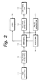
- Fig. 2 shows a block diagram of an example of the intermittent pulse generator 1 shown in the first embodiment.
- the intermittent pulse generator 1 shown in Fig. 2 intermittently generates pulses from the AC power source as mentioned above.
- a predetermined time constant is set by a resistor and a capacitor.
- a switching circuit 13 is turned on.
- a power source is supplied from the switching circuit 13 to a voltage detecting circuit 14, a resetting circuit 16, and a pulse generator 17.
- the switching circuit 13 is turned off.
- pulses are generated.
- the switching circuit 13 If a voltage which is equal to or larger than a predetermined voltage is detected by the voltage detecting circuit 14 when the switching circuit 13 is ON, the switching circuit 13 is turned off through a switching OFF circuit 15. The pulses generated by turning on/off the switching circuit 13 as mentioned above are supplied to a load 18.
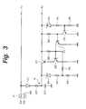
- Fig. 3 shows a circuit diagram of an example of the intermittent pulse generator 1 shown in the first embodiment.
- a diode 21 is a rectifying circuit.
- the time constant circuit 11 is constructed by a resistor 22 and a capacitor 23.
- the voltage detecting circuit 12 is constructed by a Zener diode 24 and resistors 25, 26, and 36.
- the switching circuit 13 is constructed by a pnp type transistor 27 and an npn type transistor 28.
- a resistor 29 corresponds to the resetting circuit 16.
- the switching OFF circuit 15 is constructed by a resistor 30 and npn type transistors 31 and 32.
- the voltage detecting circuit 14 is constructed by a Zener diode 33 and resistors 34 and 35.
- a collector of the transistor 27 is connected to a terminal Tc.
- the terminal Tc is connected to the controller 3.
- a terminal Ts is connected to one of the terminals on the primary side of the transformer 4 through the switching circuit 2.
- the inputted AC power source is rectified by the diode 21.
- a voltage is charged in the capacitor 23.
- a voltage at a node A of the resistor 22 and capacitor 23 is as shown in Fig.. 4A.
- the Zener diode 24 is turned on.
- the transistor 28 is turned on and the transistor 27 is turned on.
- the transistors 27 and 28 are reset by the resistor 29. The voltage is outputted through the terminal Tc until they are reset.
- the Zener diode 33 When the output voltage is equal to a reference voltage of the Zener diode 33 or less, for example, 6V or less, the Zener diode 33 is turned off.
- the transistor 32 is turned off, the transistor 31 is turned on, the transistor 28 is turned off, and the transistor 27 is turned off.
- a voltage shown in Fig. 4B is derived at a terminal Tc.
- the intermittent pulses are generated as mentioned above.
- the power source circuit is intermittently made operative by using the intermittent pulses.
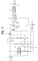
- Fig. 5 shows a specific example of the switching circuit 2 and controller 3 in the first embodiment to which the invention is applied.
- a triac (triode AC switch) 51 is used as an example of the switching circuit 2.
- the on/off operations of the triac 51 are controlled through a photocoupler 52 from a load current detecting circuit 53 provided on the secondary side of the transformer 4.
- a rectifying circuit constructed by the diode bridge 5 and capacitor 6 is connected to the load current detecting circuit 53.
- the load current detecting circuit 53 detects a load current. For example, when a current of a predetermined current value or more is detected, it is determined that the operating mode is the supplying mode.
- the triac 51 is turned on through the photocoupler 52 from the load current detecting circuit 53.
- a constant voltage circuit 54 generates a predetermined voltage for a load connected to the output terminal To.
- a light emitting diode 52s of the photocoupler 52 emits light.
- a phototransistor 52r is turned on.
- an npn type transistor 50 is turned on.
- the transistor 50 is turned on, a bias voltage is applied to a gate of the triac 51, so that the triac 51 is turned on and the inputted AC power source is supplied to the transformer 4.
- the on/off operations of the transistor 50 are controlled also by the intermittent pulse generator 1.
- a time constant circuit is constructed by a resistor 41, a capacitor 42, a resistor 46, and a capacitor 47.
- a rectifying circuit is constructed by diodes 44 and 48.
- the triac 51 is turned on by the load current detecting circuit 53. While the supply of the voltage/current to the load is stopped because of the standby mode, the triac 51 is turned on at predetermined intervals by the intermittent pulse generator 1.
- a signal shown in Fig. 4C is an example of a signal at the time of on/off controlling the triac 51 by the intermittent pulse generator 1. This signal is generated at a base of the transistor 50 and the gate of the triac 51.
- Fig. 6 shows the second embodiment of the invention.
- Fig. 6 shows the embodiment in case of applying the invention to the case of using a switching power source circuit.
- the power source inputted from the input terminal Ti is rectified by a diode bridge 60 and a capacitor 61.
- the rectified power source is supplied to the intermittent pulse generator 1.
- the intermittent pulse generator 1 supplies a signal to turn on/off an FET 65 to a PWM (pulse width modulating) circuit 63 as mentioned above.
- a signal shown in Fig. 7B is supplied from the intermittent pulse generator 1 to the PWM circuit 63.
- the signal to turn on/off the FET 65 is supplied to the intermittent pulse generator 1 from the secondary side of a transformer 66 through a photocoupler 77.
- the rectified power source is supplied to the PWM circuit 63 through a resistor 62.
- a signal is supplied from the secondary side of the transformer 66 through a photocoupler 76.
- the PWM circuit 63 supplies a signal to a gate of the FET 65 in response to the supplied signal.
- a drain of the FET 65 is connected to a winding 66a of the transformer 66 and a source is connected to the ground.
- a parasitic diode 65a is provided between the source and drain of the FET 65.
- a cathode of a diode 64 is connected to the PWM circuit 63 and an anode is connected to one of terminals of a winding 66b of the transformer 66.
- the other of the winding 66b of the transformer 66 is connected to the ground.
- One of terminals of a winding 66c serving as a secondary side of the transformer 66 is connected to a rectifying circuit constructed by a diode 67 and a capacitor 68.
- the other of the winding 66c is connected to the ground.
- a voltage which is outputted from the rectifying circuit is detected by a voltage detecting circuit 69.
- the switching circuit 72 is turned off.
- a current detecting circuit 70 if a load current of a predetermined current or less, for example, a current which is equal to or less than 1/100 of the ordinary current is detected, signals are supplied to an adder 74 and a switching circuit 75.
- the current detecting circuit 70 corresponds to the energy saving mode detecting circuit 7 in Fig. 1 mentioned above.
- a voltage detecting circuit 73 the voltage which is outputted from the output terminal To is detected.
- a signal is supplied from the voltage detecting circuit 73 to the adder 74.
- the adder 74 adds the signal from the current detecting circuit 70 and/or the signal from the voltage detecting circuit 73.
- the resultant addition signal is supplied to a light emitting diode 76s of the photocoupler 76 and supplied to the PWM circuit 63 through a phototransistor 76r of the photocoupler 76.
- a current detecting circuit 71 when a load current of a predetermined current or more is detected, a signal is supplied to the switching circuit 75.
- the current detecting circuit 71 corresponds to the supplying mode detecting circuit 9 in Fig. 1 mentioned above.
- a signal is supplied to a light emitting diode 77s of the photocoupler 77 and supplied to the intermittent pulse generator 1 through a phototransistor 77r of a phototransistor 77r of a photocoupler 77.
- Fig. 8 shows a block diagram on the secondary side of the transformer 66 in the second embodiment shown in Fig. 6.
- a power source which is outputted from a rectifying circuit is supplied to a supplying mode detecting circuit 81 and a power saving mode detecting circuit 82.
- the supplying mode and the energy saving mode are detected by the current which is detected as mentioned above.
- a signal transmitting circuit 83 a signal is transmitted to the primary side of the transformer 66 in accordance with a signal from the supplying mode detecting circuit 81 and/or the energy saving mode detecting circuit 82.
- a frequency of the intermittent pulses is also stable.
- the frequency of the intermittent pulses also fluctuates.
- a pulse signal shown in Fig. 9A is outputted from the intermittent pulse generator 1 when the input power source is stable at a desired voltage.
- a pulse signal shown in Fig. 9B is outputted from the intermittent pulse generator 1 when the input power source is lower than the desired voltage and a duration of a pause period of the intermitting operation becomes longer than that in Fig. 9A.
- a pulse signal shown in Fig. 9C is outputted from the intermittent pulse generator 1 when the input power source is higher than the desired voltage and a duration of a pause period of the intermitting operation is shorter than that in Fig. 9A.
- Fig. 10 shows the first example in which a constant voltage circuit is provided for an input section of the intermittent pulse generator 1 to thereby stabilize the input power source.
- a constant voltage circuit 91 is provided between a cathode of the diode 21 and the resistor 22.
- a capacitor 92 is inserted between the cathode of the diode 21 and the ground.
- the terminal Ts is connected to the switching circuit 2.
- a terminal Te is connected to an emitter of the transistor 27.
- Fig. 11 shows a circuit diagram of the second example in which a constant voltage circuit is provided for the input section of the intermittent pulse generator 1' shown in Fig. 6 to thereby stabilize the input power source.
- the constant voltage circuit 91 is provided between one of output terminals of the diode bridge 60 and one of terminals of the resistor 22.
- Fig. 12 shows a circuit diagram of an example of the constant voltage circuit 91.
- the constant voltage circuit 91 is constructed by a resistor 95, a Zener diode 96, and an npn type transistor 97.
- the rectified power source is supplied to the constant voltage circuit 91 through a terminal Tb.
- the Zener diode 96 When the input power source is higher than a reference voltage of the Zener diode 96, the Zener diode 96 is turned on and the transistor 97 is turned off.
- the Zener diode 96 is turned off, so that the transistor 97 is turned on.
- the constant voltage circuit 91 for the input section of the intermittent pulse generator 1', the input power source which is supplied to the intermittent pulse generator 1' can be stabilized to a desired voltage.
- Figs. 10 and 11 show the examples in which the constant voltage circuit 91 is provided at the front stage of the input of the intermittent pulse generator 1', it can be also provided in the intermittent pulse generator 1.
- Fig. 13 shows an example in which a constant current circuit is used for stabilizing the input power source.
- the constant current circuit is provided for the input section of the intermittent pulse generator 1' shown in Fig. 6, thereby stabilizing the input power source.
- a constant current circuit 102 is provided between the resistor 22 and capacitor 23.
- a filter 101 for removing noises is provided between the input terminal Ti and the diode bridge 60.
- Fig. 14 shows a circuit diagram of an example of the constant current circuit 102.
- the constant current circuit 102 is constructed by npn type transistors 105 and 107 and a resistor 106.
- Fig. 15 shows an examle in which an input voltage is detected and an input impedance of the intermittent pulse generator 1' is switched.
- the Zener diode 111 When the input voltage exceeds a reference voltage of a Zener diode 111, the Zener diode 111 is turned on, a transistor 115 is turned on, and a transistor 116 is turned off.
- the input voltage is equal to or lower than the reference voltage of the Zener diode 111, the Zener diode 111 is turned off, the npn type transistor 115 is turned off, and the npn type transistor 116 is turned on. Therefore, as shown in Fig. 16, when the input voltage exceeds a predetermined voltage Vz, the transistor 116 is turned off and an input impedance R rises.
- a pause period of the intermitting operation is shortened. If the input voltage is equal to or lower than the predetermined voltage Vz, the transistor 116 is turned on and the input impedance R decreases. At this time, as shown in Fig. 9B, a duration of the pause period of the intermitting operation becomes long.
- a time constant can be increased by increasing the input impedance R.
- the time constant can be reduced by decreasing the input impedance R. Therefore, a stable power source can be extracted from the terminal Te.
- Fig. 17 shows the third embodiment of the invention.
- Fig. 17 is an example in which a power source is used in a receiving section of the remote controller in the standby mode.
- Fig. 17 shows an example in which a power source section for the standby mode for supplying a power source to a photosensing section of the remote controller is provided separately from a main power source section.
- a thyristor 125 is provided for a control section connected to a gate of a triac 126.
- the control section is constructed by resistors 121, 123, and 124, a capacitor 122, and the thyristor 125 .
- a control signal is supplied to a gate of the thyristor 125 from the intermittent pulse generator 1' .
- the thyristor 125 is turned on/off.
- the triac 126 is turned on.
- a rectified power source is outputted through a transformer 127 from a diode bridge 128 and a capacitor 129 constructing a rectifying circuit.
- the power source rectified by the diode bridge 128 and capacitor 129 is supplied to a remote control receiving circuit 133.
- the remote control receiving circuit 133 supplies the signal to a light emitting diode 135s of a photocoupler.
- the light emitting diode 135s to which the signal was supplied emits light.
- the emitted light is received by a photodiode 135r of the photocoupler, so that the photodiode 135r is turned on.
- the main power source section will now be described.
- a thyristor 145 is turned on and a triac 146 is turned on.
- a control section is connected to a gate of the triac 146 in a manner similar to the foregoing triac 126.
- the control section is constructed by resistors 141, 142, and 144, a capacitor 143, and the thyristor 145.
- the triac 146 is turned on, the power source is supplied to a rectifying circuit constructed by a diode bridge 148 and a capacitor 149 through a filter 147 for removing noises.
- the power source rectified by the rectifying circuit is supplied to one of terminals of a winding 152a of a transformer 152.
- a drain of an FET 151 is connected to the other of the winding 152a of the transformer 152 and a source is connected to the ground.
- a PWM circuit 150 is connected to a gate of the FET 151.
- a parasitic diode 151a is provided for the FET 151.
- a rectifying circuit constructed by a diode 131 and a capacitor 132 is provided for a winding 152b of the transformer 152.
- a power source rectified by the rectifying circuit is supplied to the remote control receiving circuit 133 through a set load 134 and a diode 130.
- a rectifying circuit constructed by a diode 153 and a capacitor 154 is provided for a winding 152c of the transformer 152.
- a power source rectified by the rectifying circuit is supplied to a set load 155.
- a power source is outputted from a main power source section comprising a switching power source.
- the main power source section is turned on, the power source is supplied to the remote control receiving circuit 133 through the winding 152b of the transformer 152.
- the photocoupler is turned off, so that the triac 146 is turned off.
- a timing at which the power source is outputted from the power source section for the standby mode is determined by a capacitance of the capacitor 129.
- a capacitance of the capacitor 129 For example, as shown in Fig. 18, an interval at which the triac 126 is turned on can be selected from a range of tens of seconds to a few minutes. That is, the capacitance of the capacitor 129 is selected so as to minimize an electric power consumption in the standby mode.
- Fig. 19 shows the first example.
- Resistors 161 and 162 are serially provided between the terminals Ti1 and Ti2.
- a full-wave rectified current is extracted from a node of the resistors 161 and 162.
- the extracted full-wave rectified current is supplied to a terminal 164a of a switching circuit 164.
- a half-wave rectified current is extracted from the terminal Ti2 through a resistor 163.
- the extracted half-wave rectified current is supplied to a terminal 164b of the switching circuit 164.
- the voltage of the power source which is outputted from the diode bridge 60 is detected by a voltage detecting circuit 167 provided at a node of resistors 165 and 166.
- the voltage detecting circuit 167 supplies a signal to a switching circuit 168 in accordance with the detected voltage.
- the switching circuit 168 switches the switching circuit 164 in response to the supplied signal. For example, when a voltage of 100V is detected, the terminal 164a is selected in the switching circuit 164. When a voltage of 200V is detected by the voltage detecting circuit 167, the terminal 164b is selected in the switching circuit 164.
- the selected full-wave rectified current or the half-wave rectified current is supplied to the intermittent pulse generator 1'.
- Fig. 20 shows the second example.
- the full-wave rectified current is supplied to a terminal 172a of a switching circuit 172.
- the half-wave rectified current is supplied to a terminal 172b of the switching circuit 172.
- the full-wave rectified current which is outputted from the diode bridge 60 is supplied to a terminal 172c of the switching circuit 172 through a resistor 171.
- the terminal 172a is selected in the switching circuit 172.
- a terminal 172b is selected in the switching circuit 172.
- the terminal 172c is selected in the switching circuit 172.
- the power source can be similarly used.
- Fig. 21 shows an examle in the case where the half-wave rectified current is selected.
- the half-wave rectified current is supplied to the intermittent pulse generator 1' through the time constant circuit comprising the resistor 22 and capacitor 23.
- Fig. 22 shows another example in the case where the half-wave rectified current is selected.
- a transistor 183 is turned on/off in accordance with the half-wave rectified current which is supplied from a node of resistors 181 and 182.
- the transistor 183 is turned on, the power source which is outputted from the diode bridge 60 is supplied to the intermittent pulse generator 1'.
- a resistance of a time constant in another example shown in Fig. 22 can be suppressed to a value lower than that in Fig. 21. That is, a loss which is caused in another example shown in Fig. 22 can be suppressed to a value smaller than that in Fig. 21.
- Fig. 23 shows an example in the case where the full-wave rectified current is selected.
- the full-wave rectified current is supplied to the intermittent pulse generator 1' through a time constant circuit comprising one of the resistors 161 and 162 and a capacitor 169.
- the invention can be also applied to any electronic equipment so long as it receives an AC power source and has a standby mode.
- the invention can be also applied to a personal computer and can be also applied to a cellularphone in a charging mode, a camera-integrated type VTR, or the like.
- the switching circuit for the primary side of the transformer and turning off the switching circuit, the electric power consumption in the standby mode can be suppressed.
- the switching circuit is controlled, since the inputted AC power source is used and the intermittent pulses are generated, the electric power consumption can be further suppressed.
Landscapes
- Engineering & Computer Science (AREA)
- Power Engineering (AREA)
- Dc-Dc Converters (AREA)
- Direct Current Feeding And Distribution (AREA)
- Rectifiers (AREA)
- Electrical Discharge Machining, Electrochemical Machining, And Combined Machining (AREA)
- Air Bags (AREA)
Applications Claiming Priority (2)
| Application Number | Priority Date | Filing Date | Title |
|---|---|---|---|
| JP2000030628A JP4214649B2 (ja) | 2000-02-08 | 2000-02-08 | 電源装置およびパルス発生装置 |
| JP2000030628 | 2000-02-08 |
Publications (2)
| Publication Number | Publication Date |
|---|---|
| EP1124319A2 true EP1124319A2 (de) | 2001-08-16 |
| EP1124319A3 EP1124319A3 (de) | 2003-11-12 |
Family
ID=18555616
Family Applications (1)
| Application Number | Title | Priority Date | Filing Date |
|---|---|---|---|
| EP20010300779 Withdrawn EP1124319A3 (de) | 2000-02-08 | 2001-01-30 | Stromversorgungsgerät und Pulserzeugungsgerät |
Country Status (4)
| Country | Link |
|---|---|
| US (1) | US6462972B2 (de) |
| EP (1) | EP1124319A3 (de) |
| JP (1) | JP4214649B2 (de) |
| NO (1) | NO326602B1 (de) |
Cited By (1)
| Publication number | Priority date | Publication date | Assignee | Title |
|---|---|---|---|---|
| WO2010103458A3 (en) * | 2009-03-13 | 2010-11-11 | Koninklijke Philips Electronics N.V. | Supply circuit for supplying a switch circuit |
Families Citing this family (8)
| Publication number | Priority date | Publication date | Assignee | Title |
|---|---|---|---|---|
| TWI239710B (en) * | 2004-03-08 | 2005-09-11 | Asia Vital Components Co Ltd | Converter for converting pulse width modulation (PWM) to direct-current (DC) voltage |
| JP5343341B2 (ja) * | 2007-10-18 | 2013-11-13 | サンケン電気株式会社 | スイッチング電源装置 |
| JP5399847B2 (ja) * | 2009-10-02 | 2014-01-29 | 新日本無線株式会社 | 信号処理装置 |
| KR101582577B1 (ko) * | 2010-08-02 | 2016-01-21 | 엘지전자 주식회사 | 전기자동차 및 그 배터리의 충전제어방법. |
| US9160227B2 (en) * | 2012-12-14 | 2015-10-13 | Chicony Power Technology Co., Ltd. | Power supply apparatus with low standby power consumption |
| TWI464414B (zh) * | 2013-05-17 | 2014-12-11 | Feeling Technology Corp | 輕載電流偵測系統 |
| JP6335438B2 (ja) * | 2013-05-17 | 2018-05-30 | キヤノン株式会社 | スイッチ制御装置及び画像形成装置 |
| US9986604B2 (en) | 2014-02-26 | 2018-05-29 | Philips Lighting Holding B.V. | Driver arrangement |
Citations (2)
| Publication number | Priority date | Publication date | Assignee | Title |
|---|---|---|---|---|
| DD274308A1 (de) | 1988-07-25 | 1989-12-13 | Engels Fernsehgeraete Veb | Sperrwandler-schaltnetzteil mit bereitschaftsbetrieb |
| FR2775394A1 (fr) | 1998-02-25 | 1999-08-27 | Legrand Sa | Dispositif de reduction des pertes a vide d'un transformateur |
Family Cites Families (11)
| Publication number | Priority date | Publication date | Assignee | Title |
|---|---|---|---|---|
| JPS4891723A (de) * | 1972-03-08 | 1973-11-29 | ||
| DE2747300C2 (de) * | 1977-10-21 | 1983-12-01 | Licentia Patent-Verwaltungs-Gmbh, 6000 Frankfurt | Steuerimpulsgeberschaltungsanordnung |
| JPS6072199A (ja) * | 1983-09-29 | 1985-04-24 | Toshiba Corp | X線装置 |
| JPS62225173A (ja) * | 1986-03-25 | 1987-10-03 | Hitachi Ltd | 直流ブレ−キ用整流回路 |
| DE69514090T2 (de) * | 1995-03-31 | 2000-05-25 | St Microelectronics Srl | Oszillatorschaltung mit einer versorgungsspannungsunabhängigen Oszillatorfrequenz |
| US5682302A (en) * | 1995-04-07 | 1997-10-28 | Delta Electronic, Inc. | Adaptable power converter applying digitized-wave-generation for integrated circuit implementation |
| DE19729480A1 (de) * | 1997-07-10 | 1999-01-14 | Abb Patent Gmbh | Kapazitives Netzteil |
| TW364664U (en) * | 1997-10-01 | 1999-07-11 | Davicom Semiconductor Inc | Voltage controlling oscillator |
| US5936479A (en) * | 1997-12-24 | 1999-08-10 | Micron Technology, Inc. | Supply voltage insensitive charge/discharge type oscillator and method |
| JP3657445B2 (ja) * | 1998-01-28 | 2005-06-08 | セイコーインスツル株式会社 | 電子機器 |
| US6028491A (en) * | 1998-04-29 | 2000-02-22 | Atmel Corporation | Crystal oscillator with controlled duty cycle |
-
2000
- 2000-02-08 JP JP2000030628A patent/JP4214649B2/ja not_active Expired - Fee Related
-
2001
- 2001-01-30 EP EP20010300779 patent/EP1124319A3/de not_active Withdrawn
- 2001-02-06 US US09/777,321 patent/US6462972B2/en not_active Expired - Lifetime
- 2001-02-07 NO NO20010652A patent/NO326602B1/no not_active IP Right Cessation
Patent Citations (2)
| Publication number | Priority date | Publication date | Assignee | Title |
|---|---|---|---|---|
| DD274308A1 (de) | 1988-07-25 | 1989-12-13 | Engels Fernsehgeraete Veb | Sperrwandler-schaltnetzteil mit bereitschaftsbetrieb |
| FR2775394A1 (fr) | 1998-02-25 | 1999-08-27 | Legrand Sa | Dispositif de reduction des pertes a vide d'un transformateur |
Cited By (5)
| Publication number | Priority date | Publication date | Assignee | Title |
|---|---|---|---|---|
| WO2010103458A3 (en) * | 2009-03-13 | 2010-11-11 | Koninklijke Philips Electronics N.V. | Supply circuit for supplying a switch circuit |
| CN102349226A (zh) * | 2009-03-13 | 2012-02-08 | 皇家飞利浦电子股份有限公司 | 用于向开关电路供电的供电电路 |
| RU2537787C2 (ru) * | 2009-03-13 | 2015-01-10 | Конинклейке Филипс Электроникс Н.В. | Схема питания переключающей схемы |
| US9099879B2 (en) | 2009-03-13 | 2015-08-04 | Koninklijke Philips N.V. | Supply circuit for supplying power to a switch circuit |
| CN102349226B (zh) * | 2009-03-13 | 2016-08-17 | 皇家飞利浦电子股份有限公司 | 用于向开关电路供电的供电电路 |
Also Published As
| Publication number | Publication date |
|---|---|
| NO20010652L (no) | 2001-08-09 |
| NO20010652D0 (no) | 2001-02-07 |
| US20010012210A1 (en) | 2001-08-09 |
| EP1124319A3 (de) | 2003-11-12 |
| NO326602B1 (no) | 2009-01-19 |
| JP4214649B2 (ja) | 2009-01-28 |
| JP2001224132A (ja) | 2001-08-17 |
| US6462972B2 (en) | 2002-10-08 |
Similar Documents
| Publication | Publication Date | Title |
|---|---|---|
| CA2041696C (en) | Switched mode power supply having a discharge circuit for an auxiliary power source | |
| KR20050109045A (ko) | 스위칭 전원장치 | |
| JP2003169479A (ja) | スイッチング電源装置及びその駆動方法 | |
| WO2000036739A1 (en) | Power converter circuit and method for controlling | |
| US5838556A (en) | Switching power supply circuit | |
| US6452820B2 (en) | Power supplying apparatus and method having a primary side insulated from a secondary side | |
| US6525948B2 (en) | Apparatus and method for the detection of circuit irregularities and for circuit protection of a power supply | |
| EP1124319A2 (de) | Stromversorgungsgerät und Pulserzeugungsgerät | |
| KR100532518B1 (ko) | 스위칭 파워 서플라이의 스타팅 방법 및 스타팅 회로를구비한 스위칭 파워 서플라이 | |
| JPH11275857A (ja) | スイッチング電源回路 | |
| JPH0680385U (ja) | スイッチング電源装置 | |
| JP3037050B2 (ja) | 電源装置 | |
| JP3613731B2 (ja) | 無負荷時省電力電源装置 | |
| JP4973916B2 (ja) | 保護回路およびスイッチング電源装置 | |
| JP3841017B2 (ja) | 電子機器の電源装置およびその制御方法 | |
| EP0335605B1 (de) | Stromversorgungsschaltung eines Fernsehgerätes | |
| JP2001024967A (ja) | テレビジョン受信機 | |
| JPH08126311A (ja) | 電源装置 | |
| JP2858343B2 (ja) | スイッチング電源装置 | |
| JP2563347Y2 (ja) | Tv電源装置 | |
| JP4905776B2 (ja) | 保護回路およびスイッチング電源装置 | |
| JP3005228B2 (ja) | 充電回路 | |
| KR200171802Y1 (ko) | 스위칭 모드 전원 공급 장치 | |
| JP2003111397A (ja) | スイッチング電源装置の制御方法およびスイッチング電源装置 | |
| JPH048703Y2 (de) |
Legal Events
| Date | Code | Title | Description |
|---|---|---|---|
| PUAI | Public reference made under article 153(3) epc to a published international application that has entered the european phase |
Free format text: ORIGINAL CODE: 0009012 |
|
| AK | Designated contracting states |
Kind code of ref document: A2 Designated state(s): AT BE CH CY DE DK ES FI FR GB GR IE IT LI LU MC NL PT SE TR |
|
| AX | Request for extension of the european patent |
Free format text: AL;LT;LV;MK;RO;SI |
|
| PUAL | Search report despatched |
Free format text: ORIGINAL CODE: 0009013 |
|
| AK | Designated contracting states |
Kind code of ref document: A3 Designated state(s): AT BE CH CY DE DK ES FI FR GB GR IE IT LI LU MC NL PT SE TR |
|
| AX | Request for extension of the european patent |
Extension state: AL LT LV MK RO SI |
|
| RIC1 | Information provided on ipc code assigned before grant |
Ipc: 7H 03K 3/0231 B Ipc: 7H 04N 5/63 B Ipc: 7H 02M 7/155 A |
|
| 17P | Request for examination filed |
Effective date: 20040406 |
|
| AKX | Designation fees paid |
Designated state(s): DE FI FR GB SE |
|
| 17Q | First examination report despatched |
Effective date: 20090304 |
|
| STAA | Information on the status of an ep patent application or granted ep patent |
Free format text: STATUS: THE APPLICATION IS DEEMED TO BE WITHDRAWN |
|
| 18D | Application deemed to be withdrawn |
Effective date: 20150801 |