EP1122822B1 - Verbinder - Google Patents
Verbinder Download PDFInfo
- Publication number
- EP1122822B1 EP1122822B1 EP00310919A EP00310919A EP1122822B1 EP 1122822 B1 EP1122822 B1 EP 1122822B1 EP 00310919 A EP00310919 A EP 00310919A EP 00310919 A EP00310919 A EP 00310919A EP 1122822 B1 EP1122822 B1 EP 1122822B1
- Authority
- EP
- European Patent Office
- Prior art keywords
- board
- contact
- insertion part
- connector
- deployed
- Prior art date
- Legal status (The legal status is an assumption and is not a legal conclusion. Google has not performed a legal analysis and makes no representation as to the accuracy of the status listed.)
- Expired - Lifetime
Links
- 238000003780 insertion Methods 0.000 claims description 51
- 230000037431 insertion Effects 0.000 claims description 49
- 239000012212 insulator Substances 0.000 claims description 27
- 230000007246 mechanism Effects 0.000 claims description 18
- 238000003825 pressing Methods 0.000 claims description 7
- 230000002265 prevention Effects 0.000 claims 1
- 238000010586 diagram Methods 0.000 description 14
- 238000000034 method Methods 0.000 description 11
- 230000008569 process Effects 0.000 description 11
- 229910000679 solder Inorganic materials 0.000 description 10
- 238000005476 soldering Methods 0.000 description 7
- 230000003014 reinforcing effect Effects 0.000 description 4
- 230000004907 flux Effects 0.000 description 3
- 238000005406 washing Methods 0.000 description 3
- 239000011248 coating agent Substances 0.000 description 2
- 238000000576 coating method Methods 0.000 description 2
- 230000006378 damage Effects 0.000 description 2
- 238000007598 dipping method Methods 0.000 description 2
- 230000000694 effects Effects 0.000 description 2
- 238000002844 melting Methods 0.000 description 2
- 230000008018 melting Effects 0.000 description 2
- 238000004064 recycling Methods 0.000 description 2
- 239000000126 substance Substances 0.000 description 2
- 229910000978 Pb alloy Inorganic materials 0.000 description 1
- 229910001128 Sn alloy Inorganic materials 0.000 description 1
- 230000002411 adverse Effects 0.000 description 1
- 229910045601 alloy Inorganic materials 0.000 description 1
- 239000000956 alloy Substances 0.000 description 1
- 239000004020 conductor Substances 0.000 description 1
- 238000005520 cutting process Methods 0.000 description 1
- 238000005516 engineering process Methods 0.000 description 1
- 238000004519 manufacturing process Methods 0.000 description 1
- 239000000463 material Substances 0.000 description 1
- 239000002184 metal Substances 0.000 description 1
- 229910052751 metal Inorganic materials 0.000 description 1
- 230000002093 peripheral effect Effects 0.000 description 1
- 230000007704 transition Effects 0.000 description 1
Images


Classifications
-
- H—ELECTRICITY
- H01—ELECTRIC ELEMENTS
- H01R—ELECTRICALLY-CONDUCTIVE CONNECTIONS; STRUCTURAL ASSOCIATIONS OF A PLURALITY OF MUTUALLY-INSULATED ELECTRICAL CONNECTING ELEMENTS; COUPLING DEVICES; CURRENT COLLECTORS
- H01R12/00—Structural associations of a plurality of mutually-insulated electrical connecting elements, specially adapted for printed circuits, e.g. printed circuit boards [PCB], flat or ribbon cables, or like generally planar structures, e.g. terminal strips, terminal blocks; Coupling devices specially adapted for printed circuits, flat or ribbon cables, or like generally planar structures; Terminals specially adapted for contact with, or insertion into, printed circuits, flat or ribbon cables, or like generally planar structures
- H01R12/70—Coupling devices
- H01R12/71—Coupling devices for rigid printing circuits or like structures
- H01R12/72—Coupling devices for rigid printing circuits or like structures coupling with the edge of the rigid printed circuits or like structures
- H01R12/721—Coupling devices for rigid printing circuits or like structures coupling with the edge of the rigid printed circuits or like structures cooperating directly with the edge of the rigid printed circuits
-
- H—ELECTRICITY
- H01—ELECTRIC ELEMENTS
- H01R—ELECTRICALLY-CONDUCTIVE CONNECTIONS; STRUCTURAL ASSOCIATIONS OF A PLURALITY OF MUTUALLY-INSULATED ELECTRICAL CONNECTING ELEMENTS; COUPLING DEVICES; CURRENT COLLECTORS
- H01R12/00—Structural associations of a plurality of mutually-insulated electrical connecting elements, specially adapted for printed circuits, e.g. printed circuit boards [PCB], flat or ribbon cables, or like generally planar structures, e.g. terminal strips, terminal blocks; Coupling devices specially adapted for printed circuits, flat or ribbon cables, or like generally planar structures; Terminals specially adapted for contact with, or insertion into, printed circuits, flat or ribbon cables, or like generally planar structures
- H01R12/70—Coupling devices
- H01R12/7005—Guiding, mounting, polarizing or locking means; Extractors
-
- H—ELECTRICITY
- H01—ELECTRIC ELEMENTS
- H01R—ELECTRICALLY-CONDUCTIVE CONNECTIONS; STRUCTURAL ASSOCIATIONS OF A PLURALITY OF MUTUALLY-INSULATED ELECTRICAL CONNECTING ELEMENTS; COUPLING DEVICES; CURRENT COLLECTORS
- H01R24/00—Two-part coupling devices, or either of their cooperating parts, characterised by their overall structure
- H01R24/38—Two-part coupling devices, or either of their cooperating parts, characterised by their overall structure having concentrically or coaxially arranged contacts
- H01R24/40—Two-part coupling devices, or either of their cooperating parts, characterised by their overall structure having concentrically or coaxially arranged contacts specially adapted for high frequency
- H01R24/50—Two-part coupling devices, or either of their cooperating parts, characterised by their overall structure having concentrically or coaxially arranged contacts specially adapted for high frequency mounted on a PCB [Printed Circuit Board]
-
- H—ELECTRICITY
- H01—ELECTRIC ELEMENTS
- H01R—ELECTRICALLY-CONDUCTIVE CONNECTIONS; STRUCTURAL ASSOCIATIONS OF A PLURALITY OF MUTUALLY-INSULATED ELECTRICAL CONNECTING ELEMENTS; COUPLING DEVICES; CURRENT COLLECTORS
- H01R24/00—Two-part coupling devices, or either of their cooperating parts, characterised by their overall structure
- H01R24/38—Two-part coupling devices, or either of their cooperating parts, characterised by their overall structure having concentrically or coaxially arranged contacts
- H01R24/40—Two-part coupling devices, or either of their cooperating parts, characterised by their overall structure having concentrically or coaxially arranged contacts specially adapted for high frequency
- H01R24/54—Intermediate parts, e.g. adapters, splitters or elbows
- H01R24/542—Adapters
-
- H—ELECTRICITY
- H01—ELECTRIC ELEMENTS
- H01R—ELECTRICALLY-CONDUCTIVE CONNECTIONS; STRUCTURAL ASSOCIATIONS OF A PLURALITY OF MUTUALLY-INSULATED ELECTRICAL CONNECTING ELEMENTS; COUPLING DEVICES; CURRENT COLLECTORS
- H01R24/00—Two-part coupling devices, or either of their cooperating parts, characterised by their overall structure
- H01R24/58—Contacts spaced along longitudinal axis of engagement
-
- H—ELECTRICITY
- H01—ELECTRIC ELEMENTS
- H01R—ELECTRICALLY-CONDUCTIVE CONNECTIONS; STRUCTURAL ASSOCIATIONS OF A PLURALITY OF MUTUALLY-INSULATED ELECTRICAL CONNECTING ELEMENTS; COUPLING DEVICES; CURRENT COLLECTORS
- H01R2103/00—Two poles
-
- H—ELECTRICITY
- H01—ELECTRIC ELEMENTS
- H01R—ELECTRICALLY-CONDUCTIVE CONNECTIONS; STRUCTURAL ASSOCIATIONS OF A PLURALITY OF MUTUALLY-INSULATED ELECTRICAL CONNECTING ELEMENTS; COUPLING DEVICES; CURRENT COLLECTORS
- H01R2107/00—Four or more poles
-
- H—ELECTRICITY
- H01—ELECTRIC ELEMENTS
- H01R—ELECTRICALLY-CONDUCTIVE CONNECTIONS; STRUCTURAL ASSOCIATIONS OF A PLURALITY OF MUTUALLY-INSULATED ELECTRICAL CONNECTING ELEMENTS; COUPLING DEVICES; CURRENT COLLECTORS
- H01R9/00—Structural associations of a plurality of mutually-insulated electrical connecting elements, e.g. terminal strips or terminal blocks; Terminals or binding posts mounted upon a base or in a case; Bases therefor
- H01R9/22—Bases, e.g. strip, block, panel
- H01R9/24—Terminal blocks
- H01R9/2408—Modular blocks
Definitions
- This invention relates to improvements in connectors comprising any of various jacks such as so-called pin jacks or single-headed jacks.
- Two types of connectors attached to printed circuit boards for connecting mainly various types of electronic device to electrical and electronic circuit components on the printed circuit board are conventionally known, namely the board plug-in type and the surface mounting type.
- the former type is configured such that connector terminals are plugged into through holes in the printed circuit board, while the latter type is configured such that the connector is mounted on the surface of the printed circuit board.
- Both of these types of connectors require soldering for securing them to the board and for electrically connecting the circuit components on the board.
- board plug-in type of connector because it must undergo the processes of flux coating, reflow treatment, solder dipping, and washing, it is necessary to consider flux resistance, reflow heat resistance, solder heat resistance, chemical resistance, and solder wettability.
- surface mounting type of connector because the processes of reflow treatment and washing must be undergone, it is necessary to consider reflow heat resistance, chemical resistance, and solder wettability.
- Both of the connectors described earlier are configured such that they are securely attached to a board by soldering.
- the strength with which it is secured by soldering is comparatively great in view of the attachment structure thereof, wherefore it is impossible in practice to separate the connector and the printed circuit board without damaging both the connector and the printed circuit board.
- the strength wherewith it is secured by soldering is weak, so the structure is made such that, when used, the area surrounding the points of attachment of both members is reinforced so that the pattern on the printed circuit board does not peel away, wherefore, as in the case described above, it is impossible in practice to separate the connector from the printed circuit board without damaging the connector and the board.
- solder made of alloys of tin and lead considered to have comparatively low melting point while fully cognizant of the adverse effects which lead has on the environment.
- solder so long as solder is used for securely attaching the connector to the printed circuit board, other problems arise because of the various processes required in soldering operations which are unfavourable to the natural environment, namely flux coating, reflow treatment, solder dipping, and washing, etc.
- EP 0642195 which is considered to represent the closest prior art discloses an edge connector for a printed circuit board, the connector comprising a receiving groove, means for clamping the circuit board in a fixed position, and contact terminals providing electrical contact between the connector and the circuit board.
- the connector of EP 0642195 has sockets for receiving the ends of conductor cables and securing screws for fixing the cable ends in the sockets, whereby the cables are connected to the edge connector.
- an object of the present invention is to provide a connector which can be attached to a board with adequate attachment strength but without requiring soldering, and which can be easily removed from the board without causing damage.
- a connector comprising:
- the board positioned at the prescribed position by the positioning mechanism is clamped with such pressing force that the connector will not break away from the prescribed position, under conditions of ordinary use, due to the clamping mechanism.
- the connector can be attached to the board with adequate attachment strength without performing soldering. For that reason, the connector can be removed from the board easily without damaging either the connector or the board.
- Fig. 1 is a diagonal view, as seen from the front, of a board insertion type of pin jack connector in a first embodiment aspect of a connector relating to the present invention.
- Fig. 2 is a front elevation of the pin jack connector diagrammed in Fig. 1.
- Fig. 3 is a diagonal view of the pin jack connector diagrammed in Fig. 1 as seen from the back side.
- Fig. 4 is a bottom view of the pin jack connector diagrammed in Fig. 1.
- Fig. 5 is a right side elevation of the pin jack connector diagrammed in Fig. 1.
- Fig. 6 is a diagram for describing the operation of a board insertion unit comprised by the pin jack connector diagrammed in Fig. 1.
- the connector described above comprises a main body 1 configured so that it presents a roughly L shaped appearance as seen from the side, one or a plurality (six in the drawing) of cylindrical pin jacks 3 1 (to 3 n (to 3 6 in the drawing)) provided on the front of the main body 1, and a board insertion part 5, in the base part 1a of the main body 1, having a gap formed in a slit shape in the lateral direction.
- the connector described above is also provided with a plurality (four in the drawing) of ribs 7 1 (to 7 n (7 4 in the drawing)) deployed in parallel at a prescribed interval on the back side from the base part 1a to the upright part 1b for reinforcing the upright part 1b of the main body 1.
- the connector described above is also provided with a plurality (two in the drawing) of catches 9 1 (to 9 n , to 9 2 in the drawing) deployed on the upper surface of the upright part 1b, and with a plurality (two in the drawing) of catches 11 1 (to 11 n , to 11 2 in the drawing) deployed on the bottom surface of the upright part 1b.
- the connector described above is further provided with two slit shaped through holes 13a and 13b that pass from the front side of the upright part 1b to the back side thereof, and with cylindrical screw-fastening through holes 15a and 15b that pass from the front side of the upright part 1b to the back side thereof.
- the symbols 21c and 21d in Fig. 4 both denote holes that are formed in outer contacts that will be described subsequently.
- Each of the pin jacks 3 1 to 3 6 has an outer contact, an insulator, and a center contact, and the insulators have cylindrical plug insertion parts.
- the insulators have cylindrical plug insertion parts.
- two outer contacts, six insulators, and six center contacts are used.
- pieces that make contact with wiring rounds (a type of wiring pattern deployed on printed circuit boards, electrically connecting electrical and electronic circuit components on the printed circuit board; to be described subsequently), and which are part of the center contacts described above, extend from the upright part 1b at equal intervals.
- wiring rounds a type of wiring pattern deployed on printed circuit boards, electrically connecting electrical and electronic circuit components on the printed circuit board; to be described subsequently
- the center contacts described above extend from the upright part 1b at equal intervals.
- pieces that make contact with the wiring rounds and that are parts of the outer contacts described above extend from the upright part 1b at equal intervals.
- the screw fastening through holes 15a and 15b each have female threads. Into these female threads are screwed bolts, respectively, to enhance the strength of attachment toward a panel of the main body 1 that is securely attached to a printed circuit board secured to the panel. These bolts secure the main body 1 to the panel by clamping the panel with the upright part 1b.
- the catches 9 1 , 9 2 , 11 1 , and 11 2 are for use when securely attaching the outer contact to the main body 1.
- the board insertion part 5, as diagrammed in Fig. 1, 3, and 5, is open in a total of three directions, namely at the edge surface of the base part 1a opposing the back side of the upright part 1b, and on the left and right sides as seen from the back side of the upright part 1b.
- this opening on the top surface and bottom surface of the part closer to the edge surface of the base part 1a, are provided a plurality of projections (with only those indicated by the symbols 17a and 17b being described in the drawings).
- the several projections provided on the top surface, beginning with the projection 17a, and the several projections provided on the bottom surface, beginning with the projection 17b, are provided in respectively opposing positions.
- the board insertion part 5 is configured so that the opening therein is expandable in the directions of the arrows (that is, in the up and down directions) as represented in Fig. 6.
- Fig. 7 is a diagram of the inner structure of the pin jack connector configured as in the foregoing, represented as a cross-section from the A-A' line in Fig. 2.
- the back side of the upright part 1b and the base part 1a that projects laterally from the lower part of that back side so as to present a roughly L shape with the upright part 1b and that forms the outer frame which configures the board insertion part 5 are integrally configured by a member (base) 19 called a base. Portions of the base 19 form the plurality of catches 9 2 (9 1 ) and 11 2 (11 1 ), described earlier, that are on the upper surface and lower surface of the upright part 1b, respectively.
- the front side of the upper part 1b and the outer frames of the pin jacks (with only those marked by the symbols 3 4 , 3 5 , and 3 6 indicated in the drawings) that present a cylindrical shape as described earlier are configured integrally by members (outer contacts) 21 called outer contacts. That is, by attaching the outer contacts 21 to the base 19 described earlier, the outer frame of the main body 1 and the outer frame of the pin jacks 3 4 to 3 6 (3 1 to 3 3 ) are formed.
- a plurality of insulators (with only those marked by the symbols 23 4 to 23 6 being indicated in the drawings) having plug insertion parts presenting cylindrical shapes.
- a plurality of ribs (diagrammed in Fig. 8) oriented in the long axial direction thereof. The parts of the ribs closer to the base end, either in whole or in part, project in the direction of the plug insertion part axis and form fixation parts with the outer contacts 21 (cf. Fig. 8).
- the parts of the insulators 23 4 to 23 6 (23 1 to 23 3 ) on the tip end have outer diameters that are slightly smaller than the inner diameters of the parts of the outer contacts 21 described above.
- the insulators 23 4 to 23 6 (23 1 to 23 3 ) are interposed inside the outer contacts 21, either in a condition wherein each of the parts on the tip end are made to adhere to the inner circumferential surfaces of the parts of the outer contacts 21 described above, or in a condition wherein each fixation part is fixed in the outer frame on the front side of the upright part 1b constituted by the outer contacts 21.
- center contact in the center contacts 25 1 to 25 6 There are three types of center contact in the center contacts 25 1 to 25 6 , namely a type (symbols 25 6 and 25 1 ) corresponding to the uppermost level of pin jacks 3 6 (3 1 ), a type (symbols 25 5 and 25 2 ) corresponding to the middle level of pin jacks 3 5 (3 2 ), and a type (symbols 25 4 and 25 3 ) corresponding to the lowermost level of pin jacks 3 4 (3 3 ). All of these are formed in an overall flat plate shape with thin walls, and each comprises a plug side contact part P that makes contact with a plug, and a wiring round side contact part W that makes contact with (a) wiring round(s) (described subsequently) on the printed circuit board.
- the plug side contact part P has a pair of contact points near the tip end, presenting a comparatively large shape.
- the wiring round side contact part W has a pair of contact points, also near the tip end, but, unlike the plug side contact P, presenting a comparatively small shape.
- the plug side contact part P and the wiring round side contact part W are configured such that they have spring forces that act in directions that fasten an inserted plug or the parts of an inserted printed circuit board where wiring rounds are deployed, respectively. Because of these spring forces, the plug side contact part P clamps the plug with a force of such strength that the plug will not break away from the plug side contact part P, unless an inserted plug is pulled out by main force. Similarly, due to the spring forces noted above, the wiring round side contact part W clamps the printed circuit board with such strength that the printed circuit board will not break away from the wiring round side contact part W unless an inserted printed circuit board is removed by main force.
- the printed circuit board clamping structure effected by the wiring round side contact part W will be described in greater detail with reference to Fig. 14.
- connection is made between the two contact parts P and W noted above by a comparatively long contact part.
- connection is made between the two contact parts P and W by a comparatively short contact part.
- the center contact 25 4 (25 3 ) corresponding to the lowermost level pin jack 3 4 (3 3 ) . the two contact parts P and W are joined directly.
- Fig. 8 to 11 are diagonal views representing the assembly process for a pin jack connector having the configuration described in the foregoing.
- a center contact 25 6 (25 1 ) having a comparatively long connection part is inserted into the insulator 23 6 (23 1 ) in order to configure the uppermost level pin jack 3 6 (3 1 ).
- a center contact 25 5 (25 2 ) having a comparatively short connection part is inserted into the insulator 23 5 (23 2 ) in order to configure the middle level pin jack 3 5 (3 2 ).
- a center contact 25 4 (25 3 ) wherein the two connection parts P and W are joined directly is inserted into the insulator 23 4 (23 3 ) in order to configure the lowermost level pin jack 3 4 (3 3 ).
- the assembly 27 6 (27 1 ) described above is inserted into a place corresponding to the uppermost level pin jack 3 6 (3 1 ) in the main body 1 described earlier
- the assembly 27 5 (27 2 ) described above is inserted into a place corresponding to the middle level pin jack 3 5 (3 2 )
- the assembly 27 4 (27 3 ) described above is inserted into a place corresponding to the lowermost level pin jack 3 4 (3 3 ).
- the catch 9 1 described earlier is fixed in a hole 21a provided in the outer contact 21 (diagrammed in Fig. 10)
- the catch 11 1 described earlier is fixed in a hole 21c (diagrammed in Fig. 4).
- the outer contact 21 wherein the plug side contact part P and the wiring round side contact part W are integrally configured is securely attached to the main body 1 in the same manner as the center contacts (25 1 to 25 6 ).
- the pin jacks 3 6 , 3 5 , and 3 4 positioned in the left half of the pin jack connector described above, as seen from the front thereof, are completed.
- the pin jacks (3 1 , 3 2 , and 3 3 ) positioned in the right half of the pin jack connector as seen from the front are completed by the same processes as those described in the foregoing.
- Fig. 12 is a diagonal view, as seen from the front, of the pin jack connector having the configuration described in the foregoing when securely attached to a printed circuit board and a panel.
- the pin jack connector is secured so that it is clamped by a panel 29 and a printed circuit board 31 secured to the panel 29.
- Bolts (not shown) are screwed into the bolt,fastening through holes 15a and 15b diagrammed respectively in Fig. 2, 3, and 11, and the panel 29 is clamped by those bolts, resulting in a structure wherein the strength wherewith the connector is attached to the panel 29 and the printed circuit board 31 is increased.
- Fig. 13 is a diagonal view of the pin jack connector relating to the first embodiment aspect securely attached to a printed circuit board, with a cross section cut away in the vertical direction, as seen from the back side.
- the printed circuit board 31 has a roughly U shaped section cut out in the part that is inserted into the pin jack connector, as diagrammed, and L shaped cutouts 33a and 35a are formed at the inner peripheries on the tip ends of a pair of projections 33 and 35 formed by that cutting out.
- a plurality of wiring rounds 37 are deployed, while on the lower surface thereof also are deployed wiring rounds (not shown) similar to the wiring rounds 37.
- a pair of cutouts 19a and 19b are made in the two side ends, in the left and right directions, in the base 19, as seen from the back side, and projections 19d (19c) are formed at innermost parts of the cutouts 19a and 19b.
- a plurality of slits 39 are formed, at positions corresponding to the wiring rounds 37 noted earlier, oriented from the direction of the back side of the connector main body 1 toward the direction of the front side, passing from the upper surface to the bottom surface.
- the wiring round side contact parts W of the center contacts (25 1 to 25 6 ) described earlier and the wiring round side contact parts W 21 of the outer contact 21 are made to face the slits 39.
- the wiring round side contact parts W 21 as will be described below, when the printed circuit board 31 has been inserted as far as a prescribed position in the board insertion part 5, are deployed inside the slits 39, in a condition wherein the wiring rounds 37 described earlier are clamped from above and below, so that electrical connection with the wiring rounds 37 is made possible.
- Fig. 14 is a diagonal view of the structure wherewith the pin jack connector relating to the first embodiment aspect is attached to a printed circuit board, with a cross section cut away in the vertical direction, as seen from the direction of the back side, being a diagonal view that clearly diagrams the main parts.
- Fig. 14 is represented a condition wherein the wiring rounds 37 deployed on the upper surface and lower surface, respectively, at a place positioned at the extreme diagonal lower right point on the printed circuit board 31, are clamped, from above and below, by the upper portion of the wiring round side contact part W of the center contact 25 4 , indicated by the solid line, which faces the slit (39) positioned at the extreme diagonal lower right point on the base 19, and by the lower portion of the wiring round side contact part W, indicated by the broken line.
- the places on the printed circuit board 31 where the wiring rounds 37 are deployed, on the upper surface and the lower surface, are clamped by the wiring round side contact parts W described earlier, by spring forces which develop in the upper portions and lower portions of the wiring round side contact parts W of the center contact 25 4 and act in directions to fasten those places.
- Other places (on the upper and lower surfaces) on the printed circuit board 31 where wiring rounds 37 are deployed are clamped by such spring forces in the upper portions (indicated by solid lines) and in the lower portions thereof (not shown) of the wiring round side contact parts W of the respectively corresponding center contacts.
- Fig. 15 is a diagram of the structure wherewith the pin jack connector relating to the first embodiment aspect is attached to a printed circuit board, as seen from the front.
- Fig. 16 is a diagram of that attachment structure seen from the back side.
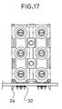
- Fig. 17 is a diagram of a structure wherewith a conventional pin jack connector is attached to a printed circuit board.
- the pin jack connector relating to this embodiment aspect is structured such that, by catches 9 1 to 11 2 in the main body 1 being fixed in holes 21a to 21d in the outer contacts 21, the insulators 23 1 to 23 6 and center contacts 25 1 to 25 6 that are interposed inside the outer contacts 21 are secured so that they are clamped, so that all of the components can be completely separated merely by releasing the fixations noted above. Accordingly, it is easy to sort parts into metal parts and plastic parts, making it easy to implement product recycling.
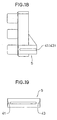
- Fig. 18 is a right side elevation of a board-insertion type of pin jack connector in a second embodiment aspect of a connector relating to the present invention.
- Fig. 19 is a diagram of a board insertion part comprised by the pin jack connector diagrammed in Fig. 18, as seen from the direction of the back side.
- This embodiment aspect differs from the first embodiment aspect described in the foregoing in that reinforcing struts 41 and 43 are formed on the left and right ends of the opening in the board insertion part 5 as seen from the back side of the upright 1b.
- reinforcing struts 41 and 43 are formed on the left and right ends of the opening in the board insertion part 5 as seen from the back side of the upright 1b.
- Fig. 20 is a diagonal view of the pin jack connector relating to the second embodiment aspect when being securely attached to a printed circuit board, with a cross section cut away in the vertical direction, as seen from the back side.
- This embodiment aspect differs from the first embodiment aspect in that there are rectangular cutouts 47 and 49 made in the printed circuit board 45, to allow passage of the reinforcing struts 41 and 43 described above at the place (cut out in a U shape as in the first embodiment aspect) of insertion in the connector, and thus to facilitate securely attaching the connector.
- the configuration is the same as in the printed circuit board 31 relating to the first embodiment aspect, and so is not further described here.
Landscapes
- Coupling Device And Connection With Printed Circuit (AREA)
- Multi-Conductor Connections (AREA)
Claims (3)
- Verbinder, umfassend:einen Mechanismus zum Bestimmen einer Befestigungsposition einer Platte, derart dass eine elektrische Verbindung zwischen der Platte und anderen elektrischen oder elektronischen Geräten bewirkt wird;einen Mechanismus zum Festklemmen der Platte, die durch den Positionierungsmechanismus in einer vorgeschriebenen Position angeordnet ist, mit solch einer Druckkraft, dass sich die Platte unter normalen Gebrauchsbedingungen nicht von der vorgeschriebenen Position trennt; wobeider Positionierungsmechanismus ein Platteneinführteil (5) zum Bewirken einer elektrischen Verbindung zwischen einer eingeführten Platte und anderen elektrischen oder elektronischen Geräten ist, und der Platteneinführteil (5) und der Klemmmechanismus innerhalb eines Hauptgehäuses (1) eingesetzt sind; dadurch gekennzeichnet, dassdie eingeführte Platte mit den anderen elektrischen oder elektronischen Geräten durch einen elektrischen Verbindungsmechanismus elektrisch verbunden ist, der vom Platteneinführteil (5) zu einer Buchse (3) zur Einführung von Steckern der anderen elektrischen oder elektronischen Geräte reicht;die Buchse (3) eine oder mehrere Stiftbuchsen ist;die Stiftbuchse (3) einen äußeren Kontakt (21), welcher Fassungen zur Einführung von Steckern der anderen elektrischen oder elektronischen Geräte aufweist und eine äußere Form davon bildet, und einen Isolator (23), der in eine innere Umfangsseite eines Innenraums eingepasst ist, der durch den äußeren Kontakt (21) definiert ist, der einzusetzen ist, aufweist;der elektrische Verbindungsmechanismus den äußeren Kontakt (21) und einen mittleren Kontakt (25) aufweist, der in eine innere Umfangsseite eines Innenraums eingepasst ist, der durch den Isolator (23) definiert ist, und sich von der inneren Umfangsseite des Isolators (23) erstreckt und bis in die Nachbarschaft einer Öffnung des Platteneinführteils (5) reicht;der mittlere Kontakt (25) ein Steckerkontaktstück (P), das sich auf der inneren Umfangsseite des Isolators (23) entfaltet, und ein Plattenkontaktstück (W), das sich im Platteneinführteil (5) entfaltet, aufweist;der äußere Kontakt (21) ein Steckerkontaktstück (P), das sich auf einer äußeren Umfangsseite des Isolators (23) entfaltet, und ein Plattenkontaktstück (W), das sich im Platteneinführteil (5) entfaltet, aufweist;die Steckerkontaktstücke (P) einen Stecker, der von der Fassung des äußeren Kontakts (21) in die Stiftbuchse (3) eingeführt ist, mit solch einer Druckkraft festklemmen, dass sich der Stecker unter normalen Gebrauchsbedingungen nicht von den Steckerkontaktstücken (P) trennt;die Plattenkontaktstücke (W) eine Platte, die in den Platteneinführteil (5) eingeführt ist, mit solch einer Druckkraft festklemmen, dass sich die Platte unter normalen Gebrauchsbedingungen nicht von den Plattenkontaktstücken (W) trennt; undder Klemmmechanismus den mittleren Kontakt (25) und das Plattenkontaktstück (W) des äußeren Kontakts (21) aufweist.
- Verbinder nach Anspruch 1, wobei der Platteneinführteil (5) Verformungsverhinderungsrippen (7) in der Öffnung davon aufweist, und der Platteneinführteil (5) so ausgelegt ist, dass die Einführposition der Platte an einer Position derart fixiert wird, dass Verdrahtungsumläufe (37), die sich auf der Platte ausbreiten, durch die Plattenkontaktstücke (W) festgeklemmt werden.
- Verbinder nach Anspruch 2, wobei Fixierungslöcher (21a - 21d) an geeigneten Stellen auf dem äußeren Kontakt (21) ausgebildet sind; Arretierungen (9, 11), welche die Fixierungslöcher (21a - 21d) fixieren, an geeigneten Stellen auf dem Hauptgehäuse (1) ausgebildet sind; und der Befestigungszustand zwischen dem äußeren Kontakt (21), dem Isolator (23), dem mittleren Kontakt (25) und dem Hauptgehäuse (1) durch Freigeben der Arretierungen (9, 11) in den Fixierungslöchern (21a-21d) gelöst wird.
Priority Applications (9)
| Application Number | Priority Date | Filing Date | Title |
|---|---|---|---|
| EP05076882A EP1601066A3 (de) | 2000-02-03 | 2000-12-08 | Elektrischer Verbinder |
| EP05076879A EP1601057A3 (de) | 2000-02-03 | 2000-12-08 | Elektrischer Verbinder |
| EP05076884A EP1603198A1 (de) | 2000-02-03 | 2000-12-08 | Elektrischer Verbinder |
| EP05076878A EP1601060B1 (de) | 2000-02-03 | 2000-12-08 | Elektrischer Verbinder |
| EP05076877A EP1601056A3 (de) | 2000-02-03 | 2000-12-08 | Elektrischer Verbinder |
| EP05076876A EP1601055B1 (de) | 2000-02-03 | 2000-12-08 | Elektrischer Verbinder |
| EP05076883A EP1601058A3 (de) | 2000-02-03 | 2000-12-08 | Elektrischer Verbinder |
| EP05076875A EP1601065A3 (de) | 2000-02-03 | 2000-12-08 | Elektrischer Verbinder |
| EP05076885A EP1601059A3 (de) | 2000-02-03 | 2000-12-08 | Elektrischer Verbinder |
Applications Claiming Priority (2)
| Application Number | Priority Date | Filing Date | Title |
|---|---|---|---|
| JP2000032612A JP3393839B2 (ja) | 2000-02-03 | 2000-02-03 | コネクタ |
| JP2000032612 | 2000-02-03 |
Related Child Applications (9)
| Application Number | Title | Priority Date | Filing Date |
|---|---|---|---|
| EP05076884A Division EP1603198A1 (de) | 2000-02-03 | 2000-12-08 | Elektrischer Verbinder |
| EP05076882A Division EP1601066A3 (de) | 2000-02-03 | 2000-12-08 | Elektrischer Verbinder |
| EP05076876A Division EP1601055B1 (de) | 2000-02-03 | 2000-12-08 | Elektrischer Verbinder |
| EP05076883A Division EP1601058A3 (de) | 2000-02-03 | 2000-12-08 | Elektrischer Verbinder |
| EP05076877A Division EP1601056A3 (de) | 2000-02-03 | 2000-12-08 | Elektrischer Verbinder |
| EP05076885A Division EP1601059A3 (de) | 2000-02-03 | 2000-12-08 | Elektrischer Verbinder |
| EP05076878A Division EP1601060B1 (de) | 2000-02-03 | 2000-12-08 | Elektrischer Verbinder |
| EP05076879A Division EP1601057A3 (de) | 2000-02-03 | 2000-12-08 | Elektrischer Verbinder |
| EP05076875A Division EP1601065A3 (de) | 2000-02-03 | 2000-12-08 | Elektrischer Verbinder |
Publications (3)
| Publication Number | Publication Date |
|---|---|
| EP1122822A2 EP1122822A2 (de) | 2001-08-08 |
| EP1122822A3 EP1122822A3 (de) | 2003-06-18 |
| EP1122822B1 true EP1122822B1 (de) | 2006-03-29 |
Family
ID=18557186
Family Applications (10)
| Application Number | Title | Priority Date | Filing Date |
|---|---|---|---|
| EP05076876A Expired - Lifetime EP1601055B1 (de) | 2000-02-03 | 2000-12-08 | Elektrischer Verbinder |
| EP05076882A Withdrawn EP1601066A3 (de) | 2000-02-03 | 2000-12-08 | Elektrischer Verbinder |
| EP05076885A Withdrawn EP1601059A3 (de) | 2000-02-03 | 2000-12-08 | Elektrischer Verbinder |
| EP00310919A Expired - Lifetime EP1122822B1 (de) | 2000-02-03 | 2000-12-08 | Verbinder |
| EP05076877A Withdrawn EP1601056A3 (de) | 2000-02-03 | 2000-12-08 | Elektrischer Verbinder |
| EP05076884A Withdrawn EP1603198A1 (de) | 2000-02-03 | 2000-12-08 | Elektrischer Verbinder |
| EP05076875A Withdrawn EP1601065A3 (de) | 2000-02-03 | 2000-12-08 | Elektrischer Verbinder |
| EP05076879A Withdrawn EP1601057A3 (de) | 2000-02-03 | 2000-12-08 | Elektrischer Verbinder |
| EP05076878A Expired - Lifetime EP1601060B1 (de) | 2000-02-03 | 2000-12-08 | Elektrischer Verbinder |
| EP05076883A Withdrawn EP1601058A3 (de) | 2000-02-03 | 2000-12-08 | Elektrischer Verbinder |
Family Applications Before (3)
| Application Number | Title | Priority Date | Filing Date |
|---|---|---|---|
| EP05076876A Expired - Lifetime EP1601055B1 (de) | 2000-02-03 | 2000-12-08 | Elektrischer Verbinder |
| EP05076882A Withdrawn EP1601066A3 (de) | 2000-02-03 | 2000-12-08 | Elektrischer Verbinder |
| EP05076885A Withdrawn EP1601059A3 (de) | 2000-02-03 | 2000-12-08 | Elektrischer Verbinder |
Family Applications After (6)
| Application Number | Title | Priority Date | Filing Date |
|---|---|---|---|
| EP05076877A Withdrawn EP1601056A3 (de) | 2000-02-03 | 2000-12-08 | Elektrischer Verbinder |
| EP05076884A Withdrawn EP1603198A1 (de) | 2000-02-03 | 2000-12-08 | Elektrischer Verbinder |
| EP05076875A Withdrawn EP1601065A3 (de) | 2000-02-03 | 2000-12-08 | Elektrischer Verbinder |
| EP05076879A Withdrawn EP1601057A3 (de) | 2000-02-03 | 2000-12-08 | Elektrischer Verbinder |
| EP05076878A Expired - Lifetime EP1601060B1 (de) | 2000-02-03 | 2000-12-08 | Elektrischer Verbinder |
| EP05076883A Withdrawn EP1601058A3 (de) | 2000-02-03 | 2000-12-08 | Elektrischer Verbinder |
Country Status (6)
| Country | Link |
|---|---|
| US (5) | US6524118B1 (de) |
| EP (10) | EP1601055B1 (de) |
| JP (1) | JP3393839B2 (de) |
| CN (5) | CN1497789B (de) |
| DE (3) | DE60039544D1 (de) |
| TW (1) | TW483201B (de) |
Families Citing this family (42)
| Publication number | Priority date | Publication date | Assignee | Title |
|---|---|---|---|---|
| US8459157B2 (en) * | 2003-12-31 | 2013-06-11 | Sd3, Llc | Brake cartridges and mounting systems for brake cartridges |
| JP3393839B2 (ja) * | 2000-02-03 | 2003-04-07 | 株式会社日本ディックス | コネクタ |
| US7390197B2 (en) * | 2002-07-17 | 2008-06-24 | Oqo Incorporated | Electronic device with integral connectors |
| JP2004146271A (ja) * | 2002-10-25 | 2004-05-20 | Fci Asia Technology Pte Ltd | 複数段式電気コネクタ |
| US7094074B2 (en) * | 2003-09-11 | 2006-08-22 | Super Talent Electronics, Inc. | Manufacturing methods for ultra-slim USB flash-memory card with supporting dividers or underside ribs |
| US20050070138A1 (en) * | 2003-09-11 | 2005-03-31 | Super Talent Electronics Inc. | Slim USB Plug and Flash-Memory Card with Supporting Underside Ribs Engaging Socket Springs |
| US8102657B2 (en) | 2003-12-02 | 2012-01-24 | Super Talent Electronics, Inc. | Single shot molding method for COB USB/EUSB devices with contact pad ribs |
| US8998620B2 (en) * | 2003-12-02 | 2015-04-07 | Super Talent Technology, Corp. | Molding method for COB-EUSB devices and metal housing package |
| US6997742B1 (en) * | 2004-09-24 | 2006-02-14 | Meng Tung | Multi-layer connector assembly |
| US20060148314A1 (en) * | 2004-12-30 | 2006-07-06 | Motorola, Inc. | PCB mounted audio jack |
| KR100687930B1 (ko) * | 2005-08-19 | 2007-02-27 | 삼성전자주식회사 | 휴대용 컴퓨터 |
| US7264512B2 (en) * | 2005-12-21 | 2007-09-04 | International Business Machines Corporation | PCI express connector |
| JP4977367B2 (ja) * | 2005-12-26 | 2012-07-18 | 任天堂株式会社 | 電子回路モジュール、およびこれに用いられる表面実装用コネクタ |
| US7997928B2 (en) * | 2006-12-01 | 2011-08-16 | Fct Electronics, Lp | Multi-position coaxial connector system |
| US7845975B2 (en) * | 2007-01-30 | 2010-12-07 | Pulse Engineering, Inc. | Low-profile connector assembly and methods |
| US7458826B1 (en) * | 2007-08-13 | 2008-12-02 | Sony Ericsson Mobile Communications Ab | Compression connector for connecting electrical components |
| EP2360796A4 (de) | 2008-12-17 | 2012-05-16 | Fujikura Ltd | Stecker für einen universellen serienbuskonnektor und konnektoranordnung |
| WO2010087473A1 (ja) * | 2009-01-30 | 2010-08-05 | 株式会社フジクラ | 中継コネクタ |
| US8914183B2 (en) * | 2010-09-20 | 2014-12-16 | Joshua Forwerck | Enhanced electronic assembly |
| US8829348B2 (en) * | 2011-02-15 | 2014-09-09 | Commscope, Inc. Of North Carolina | Pair orbit management for communication cables |
| CN102270794B (zh) * | 2011-04-13 | 2014-01-22 | 中北大学 | Usb盲插接口 |
| US8430675B2 (en) * | 2011-06-24 | 2013-04-30 | Tyco Electronics Corporation | Edge mount electrical connector |
| US8272897B1 (en) * | 2011-08-16 | 2012-09-25 | Cheng Uei Precision Industry Co., Ltd. | Electrical connector |
| KR101923472B1 (ko) * | 2011-12-06 | 2018-11-29 | 엘지전자 주식회사 | 소켓 모듈 및 이를 구비한 단말기 |
| US8684757B2 (en) * | 2012-04-27 | 2014-04-01 | International Business Machines Corporation | Memory module connector with air deflection system |
| EP2896094B1 (de) * | 2012-09-12 | 2020-04-08 | Smiths Interconnect Americas, Inc. | Elektrischer steckverbinder |
| JP5943788B2 (ja) * | 2012-09-13 | 2016-07-05 | 日本航空電子工業株式会社 | カードエッジ型同軸コネクタ |
| JP6057372B2 (ja) * | 2013-05-02 | 2017-01-11 | 日本圧着端子製造株式会社 | コネクタ |
| CN103887643B (zh) * | 2014-03-17 | 2016-04-13 | 小米科技有限责任公司 | 耳机插座、电子器件、电子设备及电子系统 |
| US9484654B2 (en) * | 2014-04-10 | 2016-11-01 | Foxconn Interconnect Technology Limited | Electrical connector with improved contacts |
| CN107017533A (zh) * | 2016-01-28 | 2017-08-04 | 联想企业解决方案(新加坡)有限公司 | 电路板连接器 |
| CN105826779B (zh) * | 2016-03-28 | 2019-07-23 | 中航光电科技股份有限公司 | 一种转接连接器及使用该转接连接器的设备机柜 |
| CN106253026B (zh) * | 2016-08-30 | 2018-08-24 | 宁波永望电子科技有限公司 | 连接件针脚定位器 |
| CN107845864A (zh) * | 2016-09-21 | 2018-03-27 | 胡正宇 | 一种用于电路板与电连接器相连接的插接式结构 |
| DE102017105186B4 (de) * | 2017-03-10 | 2019-05-23 | Amphenol-Tuchel Electronics Gmbh | Rundsteckverbinderbuchse für eine daran anordenbare Leiterplatte |
| US10170868B1 (en) * | 2017-10-16 | 2019-01-01 | Jae Electronics, Inc. | Connector |
| BE1025734A9 (de) * | 2017-11-27 | 2019-07-03 | Phoenix Contact Gmbh & Co | Modularer Steckverbinder austauschbarer Modul-Leiterplatte |
| CN108462017B (zh) * | 2018-04-02 | 2024-01-30 | 苏州盖特龙自动化设备有限公司 | 一种电机碳刷自动化组装下料设备 |
| JP6498373B1 (ja) * | 2018-09-07 | 2019-04-10 | カナレ電気株式会社 | 同軸コネクタ装置 |
| US20210391677A1 (en) * | 2018-10-23 | 2021-12-16 | Siemens Aktiengesellschaft | Connector and three-way transmission and conversion circuit module |
| JP6923851B2 (ja) * | 2018-12-28 | 2021-08-25 | Smk株式会社 | 中継コネクタ |
| FR3098032B1 (fr) * | 2019-06-26 | 2022-02-25 | Radiall Sa | Ensemble de connexion à bornier à pluralité de modules de connexion de puissance indépendants et système de verrouillage/déverrouillage rapide des modules à un rail destiné à être fixé sur une structure, notamment une structure d’aéronef. |
Family Cites Families (31)
| Publication number | Priority date | Publication date | Assignee | Title |
|---|---|---|---|---|
| GB950104A (de) * | 1960-11-04 | 1900-01-01 | ||
| US3149893A (en) * | 1962-09-24 | 1964-09-22 | Burndy Corp | Auxiliary ground connection for a printed circuit connector |
| FR2061862A5 (de) * | 1969-07-22 | 1971-06-25 | Amp France Sa | |
| US3861775A (en) * | 1972-11-03 | 1975-01-21 | Xerox Corp | Multiple circuit board connector |
| US4174147A (en) * | 1977-03-01 | 1979-11-13 | Amerace Corporation | Circuit panel connector |
| US4364625A (en) * | 1980-06-12 | 1982-12-21 | Bell Telephone Laboratories, Incorporated | Electrical jack assembly |
| US4392708A (en) * | 1980-08-04 | 1983-07-12 | Switchcraft, Inc. | Electrical jack |
| JPS607169U (ja) * | 1983-06-25 | 1985-01-18 | 星電器製造株式会社 | 電話用コネクタ |
| JPS607169A (ja) | 1983-06-27 | 1985-01-14 | Nippon Telegr & Teleph Corp <Ntt> | Cmos集積回路 |
| JPS6051891U (ja) * | 1983-09-17 | 1985-04-11 | ヒロセ電機株式会社 | レセプタクルコネクタ |
| JPS6051890U (ja) * | 1983-09-19 | 1985-04-11 | 星電器製造株式会社 | ジヤツク |
| JPS6080685A (ja) | 1983-10-07 | 1985-05-08 | 株式会社奥村組 | 地下道構造物推進法 |
| JPS6080685U (ja) * | 1983-11-07 | 1985-06-04 | 三洋電機株式会社 | ソケツト取付装置 |
| JPS60147091U (ja) * | 1984-03-07 | 1985-09-30 | ミツミティ−ア−ルダブリュ株式会社 | コネクタ |
| US4602842A (en) * | 1984-12-03 | 1986-07-29 | Cts Corporation | Electrical connector receptacle |
| GB8510839D0 (en) * | 1985-04-29 | 1985-06-05 | Allied Corp | Electric circuit board assembly |
| GB8510840D0 (en) * | 1985-04-29 | 1985-06-05 | Allied Corp | Electrical connectors |
| JPS6243479U (de) * | 1985-09-02 | 1987-03-16 | ||
| GB8725475D0 (en) * | 1987-10-30 | 1987-12-02 | Amp Holland | Modular jack |
| US4997996A (en) * | 1987-12-17 | 1991-03-05 | Nihon Kaikeiki Kogyo Kabushiki Kaisha | Printed wiring board mounted electronic component |
| GB8811665D0 (en) * | 1988-05-17 | 1988-06-22 | Bicc Plc | Electrical connector |
| US5178557A (en) * | 1990-10-31 | 1993-01-12 | Japan Aviation Electronics Industry, Limited | Electric connector having symmetric locking blocks at opposite ends |
| DE9313402U1 (de) * | 1993-09-06 | 1995-01-12 | F. Wieland Elektrische Industrie Gmbh, 96052 Bamberg | Leiterplatte |
| CN2187346Y (zh) * | 1994-05-23 | 1995-01-11 | 富士康国际股份有限公司 | 微型连接器 |
| US5823796A (en) * | 1996-04-02 | 1998-10-20 | Itt Manufacturing Enterprises, Inc. | Audio/power jack for IC card |
| SG48362A1 (en) * | 1996-06-25 | 1998-04-17 | Thomas & Betts Corp | Single-sided straddle mount printed circuit board connector |
| JP3122716B2 (ja) * | 1996-12-26 | 2001-01-09 | 株式会社ジャルコ | 多連ピンジャック |
| JP2002515174A (ja) * | 1997-01-31 | 2002-05-21 | ザ ウィタカー コーポレーション | Pcbエッジ用コネクタ |
| US5984731A (en) * | 1997-11-17 | 1999-11-16 | Xircom, Inc. | Removable I/O device with integrated receptacles for receiving standard plugs |
| US5954521A (en) * | 1998-01-29 | 1999-09-21 | All Best Electronics Co., Ltd. | Interface card connector |
| JP3393839B2 (ja) * | 2000-02-03 | 2003-04-07 | 株式会社日本ディックス | コネクタ |
-
2000
- 2000-02-03 JP JP2000032612A patent/JP3393839B2/ja not_active Expired - Fee Related
- 2000-10-19 US US09/691,103 patent/US6524118B1/en not_active Expired - Lifetime
- 2000-11-28 TW TW089125164A patent/TW483201B/zh not_active IP Right Cessation
- 2000-12-08 EP EP05076876A patent/EP1601055B1/de not_active Expired - Lifetime
- 2000-12-08 DE DE60039544T patent/DE60039544D1/de not_active Expired - Lifetime
- 2000-12-08 DE DE60026949T patent/DE60026949T2/de not_active Expired - Lifetime
- 2000-12-08 EP EP05076882A patent/EP1601066A3/de not_active Withdrawn
- 2000-12-08 EP EP05076885A patent/EP1601059A3/de not_active Withdrawn
- 2000-12-08 EP EP00310919A patent/EP1122822B1/de not_active Expired - Lifetime
- 2000-12-08 EP EP05076877A patent/EP1601056A3/de not_active Withdrawn
- 2000-12-08 EP EP05076884A patent/EP1603198A1/de not_active Withdrawn
- 2000-12-08 DE DE60038321T patent/DE60038321T2/de not_active Expired - Lifetime
- 2000-12-08 EP EP05076875A patent/EP1601065A3/de not_active Withdrawn
- 2000-12-08 EP EP05076879A patent/EP1601057A3/de not_active Withdrawn
- 2000-12-08 EP EP05076878A patent/EP1601060B1/de not_active Expired - Lifetime
- 2000-12-08 EP EP05076883A patent/EP1601058A3/de not_active Withdrawn
- 2000-12-19 CN CN031560318A patent/CN1497789B/zh not_active Expired - Fee Related
- 2000-12-19 CN CN03156020A patent/CN100576638C/zh not_active Expired - Fee Related
- 2000-12-19 CN CNB031560229A patent/CN100428572C/zh not_active Expired - Fee Related
- 2000-12-19 CN CNB001358243A patent/CN1277334C/zh not_active Expired - Fee Related
- 2000-12-19 CN CNB031560210A patent/CN100428571C/zh not_active Expired - Fee Related
-
2002
- 2002-10-16 US US10/270,579 patent/US6854983B2/en not_active Expired - Lifetime
- 2002-10-16 US US10/270,598 patent/US6951486B2/en not_active Expired - Lifetime
- 2002-10-16 US US10/270,603 patent/US6629851B1/en not_active Expired - Lifetime
- 2002-10-16 US US10/270,692 patent/US7081011B2/en not_active Expired - Fee Related
Also Published As
Similar Documents
| Publication | Publication Date | Title |
|---|---|---|
| EP1122822B1 (de) | Verbinder | |
| EP1034983B1 (de) | Abzweigverbindergehäuse | |
| KR100952773B1 (ko) | 인쇄회로기판 연결용 버스바 터미널 | |
| US5064389A (en) | Electrical slave connector | |
| KR100371568B1 (ko) | 단자커넥터 | |
| US8925189B2 (en) | Method for assembling an electrical connector assembly | |
| US7641507B2 (en) | Cable connector | |
| US5872333A (en) | Connector fixing construction | |
| US7414194B2 (en) | Bus bar wiring board and method of assembling the same | |
| US6414245B1 (en) | Printed circuit board with bullet connector sockets | |
| JP3432378B2 (ja) | コネクタの固定構造 | |
| US11791575B2 (en) | Circuit board with U-shaped electrical terminal | |
| CN219535008U (zh) | 插针组件和电子设备 | |
| CN218215752U (zh) | 免焊型电连接装置及其电连接器 | |
| JP7215006B2 (ja) | 端子着脱装置 | |
| CN211789620U (zh) | 背面紧固式连接模块和控制盒 | |
| JP2002033166A (ja) | コネクタの固定構造 | |
| CN112713430A (zh) | 电源供应装置及其端子座 | |
| KR100362710B1 (ko) | 차량 배선용 커넥터의 방수장치 | |
| KR200243896Y1 (ko) | 원형의 커넥터단자를 겸용시킨 각형의 커넥터 구조 | |
| JP2000215784A (ja) | 電気接続箱 | |
| JP2000067995A (ja) | 高密度多極コネクタ |
Legal Events
| Date | Code | Title | Description |
|---|---|---|---|
| PUAI | Public reference made under article 153(3) epc to a published international application that has entered the european phase |
Free format text: ORIGINAL CODE: 0009012 |
|
| AK | Designated contracting states |
Kind code of ref document: A2 Designated state(s): AT BE CH CY DE DK ES FI FR GB GR IE IT LI LU MC NL PT SE TR |
|
| AX | Request for extension of the european patent |
Free format text: AL;LT;LV;MK;RO;SI |
|
| PUAL | Search report despatched |
Free format text: ORIGINAL CODE: 0009013 |
|
| AK | Designated contracting states |
Designated state(s): AT BE CH CY DE DK ES FI FR GB GR IE IT LI LU MC NL PT SE TR |
|
| AX | Request for extension of the european patent |
Extension state: AL LT LV MK RO SI |
|
| 17P | Request for examination filed |
Effective date: 20031117 |
|
| AKX | Designation fees paid |
Designated state(s): DE FR GB IT |
|
| 17Q | First examination report despatched |
Effective date: 20040309 |
|
| GRAP | Despatch of communication of intention to grant a patent |
Free format text: ORIGINAL CODE: EPIDOSNIGR1 |
|
| GRAS | Grant fee paid |
Free format text: ORIGINAL CODE: EPIDOSNIGR3 |
|
| GRAA | (expected) grant |
Free format text: ORIGINAL CODE: 0009210 |
|
| RAP1 | Party data changed (applicant data changed or rights of an application transferred) |
Owner name: NIPPON DICS CO. LTD |
|
| RIN1 | Information on inventor provided before grant (corrected) |
Inventor name: YAMAKAWA, HIROJI,C/O NIPPON DISCS CO. LTD Inventor name: KIKUCHI, EIJI,C/O NIPPON DISCS CO. LTD |
|
| AK | Designated contracting states |
Kind code of ref document: B1 Designated state(s): DE FR GB IT |
|
| PG25 | Lapsed in a contracting state [announced via postgrant information from national office to epo] |
Ref country code: IT Free format text: LAPSE BECAUSE OF FAILURE TO SUBMIT A TRANSLATION OF THE DESCRIPTION OR TO PAY THE FEE WITHIN THE PRESCRIBED TIME-LIMIT;WARNING: LAPSES OF ITALIAN PATENTS WITH EFFECTIVE DATE BEFORE 2007 MAY HAVE OCCURRED AT ANY TIME BEFORE 2007. THE CORRECT EFFECTIVE DATE MAY BE DIFFERENT FROM THE ONE RECORDED. Effective date: 20060329 |
|
| REG | Reference to a national code |
Ref country code: GB Ref legal event code: FG4D |
|
| REF | Corresponds to: |
Ref document number: 60026949 Country of ref document: DE Date of ref document: 20060518 Kind code of ref document: P |
|
| PLBE | No opposition filed within time limit |
Free format text: ORIGINAL CODE: 0009261 |
|
| STAA | Information on the status of an ep patent application or granted ep patent |
Free format text: STATUS: NO OPPOSITION FILED WITHIN TIME LIMIT |
|
| 26N | No opposition filed |
Effective date: 20070102 |
|
| EN | Fr: translation not filed | ||
| PG25 | Lapsed in a contracting state [announced via postgrant information from national office to epo] |
Ref country code: FR Free format text: LAPSE BECAUSE OF FAILURE TO SUBMIT A TRANSLATION OF THE DESCRIPTION OR TO PAY THE FEE WITHIN THE PRESCRIBED TIME-LIMIT Effective date: 20070309 |
|
| PG25 | Lapsed in a contracting state [announced via postgrant information from national office to epo] |
Ref country code: FR Free format text: LAPSE BECAUSE OF FAILURE TO SUBMIT A TRANSLATION OF THE DESCRIPTION OR TO PAY THE FEE WITHIN THE PRESCRIBED TIME-LIMIT Effective date: 20060329 |
|
| REG | Reference to a national code |
Ref country code: GB Ref legal event code: 746 Effective date: 20110905 |
|
| REG | Reference to a national code |
Ref country code: DE Ref legal event code: R084 Ref document number: 60026949 Country of ref document: DE Effective date: 20110830 |
|
| PGFP | Annual fee paid to national office [announced via postgrant information from national office to epo] |
Ref country code: DE Payment date: 20121205 Year of fee payment: 13 |
|
| PGFP | Annual fee paid to national office [announced via postgrant information from national office to epo] |
Ref country code: GB Payment date: 20121205 Year of fee payment: 13 |
|
| REG | Reference to a national code |
Ref country code: DE Ref legal event code: R119 Ref document number: 60026949 Country of ref document: DE |
|
| GBPC | Gb: european patent ceased through non-payment of renewal fee |
Effective date: 20131208 |
|
| REG | Reference to a national code |
Ref country code: DE Ref legal event code: R079 Ref document number: 60026949 Country of ref document: DE Free format text: PREVIOUS MAIN CLASS: H01R0012040000 Ipc: H01R0012500000 |
|
| REG | Reference to a national code |
Ref country code: DE Ref legal event code: R079 Ref document number: 60026949 Country of ref document: DE Free format text: PREVIOUS MAIN CLASS: H01R0012040000 Ipc: H01R0012500000 Effective date: 20140911 Ref country code: DE Ref legal event code: R119 Ref document number: 60026949 Country of ref document: DE Effective date: 20140701 |
|
| PG25 | Lapsed in a contracting state [announced via postgrant information from national office to epo] |
Ref country code: DE Free format text: LAPSE BECAUSE OF NON-PAYMENT OF DUE FEES Effective date: 20140701 |
|
| PG25 | Lapsed in a contracting state [announced via postgrant information from national office to epo] |
Ref country code: GB Free format text: LAPSE BECAUSE OF NON-PAYMENT OF DUE FEES Effective date: 20131208 |