EP1120738A2 - Speicherkarte - Google Patents
Speicherkarte Download PDFInfo
- Publication number
- EP1120738A2 EP1120738A2 EP00951891A EP00951891A EP1120738A2 EP 1120738 A2 EP1120738 A2 EP 1120738A2 EP 00951891 A EP00951891 A EP 00951891A EP 00951891 A EP00951891 A EP 00951891A EP 1120738 A2 EP1120738 A2 EP 1120738A2
- Authority
- EP
- European Patent Office
- Prior art keywords
- memory card
- main body
- setting member
- guide
- cut
- Prior art date
- Legal status (The legal status is an assumption and is not a legal conclusion. Google has not performed a legal analysis and makes no representation as to the accuracy of the status listed.)
- Granted
Links
Images





Classifications
-
- G—PHYSICS
- G06—COMPUTING OR CALCULATING; COUNTING
- G06K—GRAPHICAL DATA READING; PRESENTATION OF DATA; RECORD CARRIERS; HANDLING RECORD CARRIERS
- G06K19/00—Record carriers for use with machines and with at least a part designed to carry digital markings
- G06K19/06—Record carriers for use with machines and with at least a part designed to carry digital markings characterised by the kind of the digital marking, e.g. shape, nature, code
- G06K19/067—Record carriers with conductive marks, printed circuits or semiconductor circuit elements, e.g. credit or identity cards also with resonating or responding marks without active components
- G06K19/07—Record carriers with conductive marks, printed circuits or semiconductor circuit elements, e.g. credit or identity cards also with resonating or responding marks without active components with integrated circuit chips
- G06K19/073—Special arrangements for circuits, e.g. for protecting identification code in memory
Definitions
- the present invention relates to a memory card having writing permitting/prohibiting setting means for preventing data stored therein from being inadvertently erased or rewritten.
- writing permitting/prohibiting setting means for a memory card uses a reflective sheet or a switch.
- Figure 9 shows an isometric view of a conventional memory card 900 having writing permitting/prohibiting setting means in the form of a reflective sheet 23.
- reference numeral 21 represents a memory card main body
- reference numeral 22 represents a terminal integrally provided with the memory card main body 21
- reference numeral 23 represents the reflective sheet.
- the memory card main body 21 has a rewritable semiconductor memory (not shown) therein.
- An apparatus (not shown) electrically connected to the semiconductor memory through the terminal 22 reads and rewrites data stored in the semiconductor memory.
- the reflective sheet 23 is used as the writing permitting/prohibiting setting means. Whether writing is permitted or prohibited is set by pasting the reflective sheet 23 at a prescribed position of the memory card main body 21 or peeling off the reflective sheet 23 .
- the apparatus detects whether the writing is set to be permitted or prohibited by detecting a reflecting state of the prescribed position of the memory card main body 21 by a photocoupler or the like.
- FIG 10 is an isometric view of a conventional memory card 1000 having writing permitting/prohibiting setting means in the form of a switch 33.
- reference numeral 31 represents a memory card main body
- reference numeral 32 represents a terminal integrally provided with the memory card main body 31
- reference numeral 33 represents the switch.
- the memory card main body 31 has a rewritable semiconductor memory (not shown) therein.
- An apparatus (not shown) electrically connected to the semiconductor memory through the terminal 32 reads and rewrites data stored in the semiconductor memory.
- the switch 33 is used as the writing permitting/prohibiting setting means. Whether writing is permitted or prohibited is set by switching the switch 33 .
- the apparatus electrically detects the setting of the switch 33 through the terminal 32.
- the conventional memory card 900 having the writing permitting/prohibiting setting means in the form of the reflective sheet 23 does not have a mechanical structure for the writing permitting/prohibiting setting means, and therefore is effective to reduce the size and thickness of the memory card main body 21 .
- the memory card 900 since writing is set to be permitted or prohibited by pasting or peeling off the reflective sheet 23 , the memory card 900 is not convenient in terms of the writing permitting/prohibiting setting operation.
- the conventional memory card 1000 having the writing permitting/prohibiting setting means in the form of the switch 33 sets writing to be permitted or prohibited by switching the switch 33 , and therefore is simple in terms of the writing permitting/prohibiting setting operation.
- the memory card 1000 is limited in reduction in the size and thickness of the memory card main body 31 .
- the present invention has been made with an objective of providing a memory card having writing permitting/prohibiting setting means which is simple in terms of a setting operation and can be reduced in the size and thickness of a memory card main body.
- a memory card includes a memory card main body having a cut-out portion formed therein; a semiconductor memory in which data is at least writable; a terminal provided on the memory card main body for electrically connecting the semiconductor memory and an external apparatus; and a writing permitting/prohibiting setting member slidably engaged with the cut-out portion for setting data write to the semiconductor memory to be permitted or prohibited.
- the writing permitting/prohibiting setting member includes a main body for covering a portion of the cut-out portion. The writing permitting/prohibiting setting member slides along the cut-out portion so as to set data write to the semiconductor memory to be permitted or prohibited.
- the writing permitting/prohibiting setting member may further include an engaging piece, and a guide engaged with the engaging piece for slidably holding the writing permitting/prohibiting setting member may be formed on each of both sides of the cut-out portion.
- the engaging pieces may be elastic so as to be deformed by a contact with the memory card main body when the writing permitting/prohibiting setting member is attached to the memory card main body.
- the memory card main body may have a surface
- the writing permitting/prohibiting setting member may have a surface
- the engaging piece may be engaged with the guide so that the surface of the writing permitting/prohibiting setting member does not project from the surface of the memory card main body.
- the surface of the memory card main body may include a first surface and a second surface
- the guide may have a first guide corresponding to the first surface and a second guide corresponding to the second surface
- the engaging piece may include a first engaging piece engageable with the first guide and a second engaging piece engageable with the second guide
- the writing permitting/prohibiting setting member may have a substantially U-shaped crosssection so that the first and second engaging pieces are respectively engageable with the first and second guides and therefore the writing permitting/prohibiting setting member holds the memory card main body.
- the cut-out portion and the first and second guides may be integrally formed during a molding process for sealing the semiconductor memory.
- a first guide taper portion and a second guide taper portion respectively for guiding the first and second engaging pieces to the first and second guides when the writing permitting/prohibiting setting member may be attached to the memory card main body are formed respectively on both sides of the cut-out portion.
- a recessed portion capable of absorbing a thickness of the engaging piece may be formed on each of both sides of the cut-out portion, the guide may be formed in the recessed portion, and the engaging piece may have a projection engageable with the guide.
- the memory card main body may have a surface
- the writing permitting/prohibiting setting member may have a surface
- the engaging piece may be engaged with the guide so that the surface of the writing permitting/prohibiting setting member does not project from the surface of the memory card main body.
- the surface of the memory card main body may include a first surface and a second surface
- the guide may have a first guide corresponding to the first surface and a second guide corresponding to the second surface
- the projection may include a first projection engageable with the first guide and a second projection engageable with the second guide
- the writing permitting/prohibiting setting member may have a substantially U-shaped cross-section so that the first and second projections are respectively engageable with the first and second guides and therefore the writing permitting/prohibiting setting member holds the memory card main body.
- the cut-out portion and the first and second guides may be integrally formed during a molding process for sealing the semiconductor memory.
- a first guide taper portion and a second guide taper portion respectively for guiding the first and second projections to the first and second guides when the writing permitting/prohibiting setting member may be attached to the memory card main body are formed respectively on both sides of the cut-out portion.
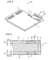
- Figure 1 is an isometric view of a memory card 100 in the first example according to the present invention in an assembled state.
- Figures 2 and 3 are exploded isometric views of the memory card 100 shown in Figure 1.
- Figure 4 is a cross-sectional view taken along the A-A line of the memory card 100 shown in Figure 1.
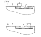
- Figure 5 is a view illustrating a setting operation of the memory card 100 shown in Figure 1.
- Figure 6 is a view illustrating setting detection of the memory card 100 shown in Figure 1.
- reference numeral 1 represents a memory card main body.
- the memory card 1 integrally has a terminal 2 for electric connection with an apparatus, and has a rewritable semiconductor memory (not shown) therein.
- the apparatus (not shown) electrically connected with the semiconductor memory through the terminal 2 reads and rewrites data stored in the semiconductor memory. For rewriting, writing permitting/prohibiting setting means described below is provided in order to prevent the stored data from being inadvertently erased or rewritten.
- Reference numeral 3 represents a cut-out portion formed on a side surface of the memory card main body 1.
- the cut-out portion 3 provides a planar shape of the memory card main body 1 with a quadrangular recess.
- a writing permitting/prohibiting setting member 4 is slidably engaged with the cut-out portion 3 .
- the writing permitting/prohibiting setting member 4 includes a main body 5 for covering a portion of the cut-out portion 3 and engaging pieces 6.
- Each engaging piece 6 is engaged with a guide groove 7 formed in the vicinity of the cut-out portion 3 of the memory card main body 1 and is slidably held.
- the engaging pieces 6 can be elastic so as to be deformed by a contact with the memory card main body 1 when the writing permitting/prohibiting setting member 4 is attached to the memory card main body 1.
- the guide grooves 7 are formed in the vicinity of the cut-out portion 3 of the memory card main body 1.
- Each guide groove 7 is lower than a surface 1S of the memory card main body 1 and is formed on each of a top surface and a bottom surface of the memory card main body 1 asymmetrically.
- the writing permitting/prohibiting setting member 4 is formed to have a substantially U-shaped cross-section so as to be held by the guide grooves 7 on the top and bottom surfaces .
- the engaging pieces 6 provided on the top and bottom surfaces so as to face each other are slidably engaged with the guide grooves 7 , respectively.
- a step D1 between the surface 1S of the memory card main body 1 and each guide groove 7 absorbs a thickness D2 of the respective engaging piece 6 of the writing permitting/prohibiting setting member 4 (the thickness D2 is the step between a surface 4S of the writing permitting/prohibiting setting member 4 and the guide groove 7 ).
- the thickness D2 is the step between a surface 4S of the writing permitting/prohibiting setting member 4 and the guide groove 7 .
- Guide taper portions 9 are formed at an end surface of the memory card main body 1 corresponding to the guide grooves 7 .
- the guide taper portions 9 each have an end surface which is thinner than the thickness of the memory card main body 1 and become thicker toward the respective guide grooves 7 .
- the guide taper portions 9 are formed on the top and bottom sides of the end surface of the memory card main body 1 in a range corresponding to the total width of the engaging pieces 6 .
- the guide taper portions 9 act as a guide for guiding the engaging pieces 6 toward the guide grooves 7 when the engaging writing permitting/prohibiting setting member 4 is to be engaged with the guide grooves 7 .
- reference numeral 10 represents stoppers. Two stoppers 10 are formed on each of the top and bottom faces in the guide grooves 7. A rib 11 ( Figure 3 ) formed on an inner surface of each of the top and bottom engaging pieces 6 so as to project inward the engaging pieces 6 are stopped by the respective stoppers 10 . The rib 11 is stopped by either one of the two stoppers 10 , and thus the writing permitting/prohibiting setting member 4 can select the position at which the cut-out portion 3 is covered.
- the cut-out portion 3 integrally formed in the memory card main body 1, the top and bottom guide grooves 7, the guide taper portions 9, and the stoppers 10 are integrally formed during a molding process for sealing the semiconductor memory.
- the writing permitting/prohibiting setting member 4 in order to engage the writing permitting/prohibiting setting member 4 with the memory card main body 1 , the writing permitting/prohibiting setting member 4 is caused to touch the memory card main body 1 so that the engaging members 6 hold the guide taper portions 9 .
- the writing permitting/prohibiting setting member 4 is pushed into the memory card main body 1 , thereby expanding the engaging pieces 6 with the guide taper portions 9 being used as a guide and thus guiding the engaging pieces 6 to the guide grooves 7 .
- the engaging pieces 6 fit in the guide grooves 7, and the writing permitting/prohibiting setting member 4 is slidably engaged with the memory card main body 1 .
- a main body 5 of the writing permitting/prohibiting setting member 4 engaged with the memory card main body 1 covers a portion of the cut-out portion 3 .
- the portion of the cut-out portion 3 which is covered is about half on the left or the right.
- the left portion is covered.
- the covered portion is substantially integral with the exterior of the memory card main body 1 .
- the substantially half portion on the right which is not covered provides the planar shape of the memory card main body 1 with a quadrangular recess.
- the writing permitting/prohibiting setting member 4 includes the projecting rib 11, and the memory card main body 1 includes the recess-type stoppers 10.
- the shape of each element is not limited to this as long as the elements are structured to be freely engageable and disengageable.
- reference numeral 13 represents an apparatus to which the memory card is inserted and connected
- reference numeral 14 represents a detection switch provided on the apparatus 13.
- the detection switch 14 includes a detection section 15 and a contact 16 .
- the writing permitting/prohibiting setting member 4 covers a left portion of the cut-out portion 3 . It is assumed that in the state where the writing permitting/prohibiting setting member 4 is positioned at the left, the data write is set to be permitted. In this state, the writing permitting/prohibiting setting member 4 covers the left portion of the cut-out portion 3 . Accordingly, the detection section 15 of the detection switch 14 is raised, thereby closing the contact 16 . By detecting the closed state of the contact 16 , the apparatus 13 can recognize that data write on the memory card 1 is permitted. The detection by the switch 14 can be performed also in the case where the position of the writing permitting/prohibiting setting member 4 is opposite.
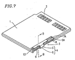
- Figure 7 is an isometric view of a memory card in a second example according to the present invention in an assembled state
- Figure 8 is a cross-sectional view taken along the B-B line of the memory card shown in Figure 7.
- recessed portioned portions 8 are formed in the vicinity of the cut-out portion 3 of the memory card main body 1 , in a range in which the writing permitting/prohibiting setting member 4 is slidable.
- a guide groove 7 is formed in each recessed portion 8.
- Each recessed portion 8 is lower than a surface 1S of the memory card main body 1 .
- the guide groove 7A which is lower than the recessed portion 8 is formed.
- Each recessed portion 8 and each guide groove 7A are formed on each of top and bottom surfaces of the memory card main body 1 asymmetrically.
- the writing permitting/prohibiting setting member 4 is formed to have a substantially U-shaped cross-section so as to be held by the recessed portion 8 on the top and bottom surfaces.
- the engaging pieces 6 are the top surface and the bottom surface of the writing permitting/prohibiting setting member 4 .
- a projection 12 is on an inner surface of each of the top and bottom engaging pieces 6 and is slidably engaged with the respective guide groove 7A . When the projections 12 are engaged with the guide grooves 7A , a step between the surface of the memory card main body 1 and each recessed portion 8 absorbs the thickness of the respective engaging piece 6 of the writing permitting/prohibiting setting member 4. Thus, each engaging piece 6 does not project from the respective surface 1S of the memory card main body 1 .
- the projection can be lengthy and formed along a longitudinal direction of each engaging piece 6 or can be short and formed in the vicinity of the tip thereof.
- a guide taper portion 9A is formed at an end surface of each of the recessed portions 8 formed in the memory card main body 1 .
- the guide taper portions 9A each have an end surface which is thinner than the thickness of the memory card main body 1 and become thicker from the end surface toward the recessed portion 8 .
- the guide taper portions 9 are formed on the top and bottom surfaces of the memory card main body 1 in a range corresponding to the total width of the engaging pieces 6.
- the guide taper portions 9 act as a guide for guiding the engaging pieces 6 toward the guide grooves 7 when the engaging writing permitting/prohibiting setting member 4 is engaged.
- the writing permitting/prohibiting setting member 4 is caused to touch the memory card main body 1 so that the projections 12 inside the engaging pieces 6 hold the guide taper portions 9.
- the writing permitting/prohibiting setting member 4 is pushed into the memory card main body 1 , thereby expanding the engaging pieces 6 each having the projection 12 , with the guide taper portions 9 being used as a guide and thus guiding the projections 12 to the guide grooves 7 .
- the projections 12 fit in the guide grooves 7, and the writing permitting/prohibiting setting member 4 is slidably engaged with the memory card main body 1 .
- the projection 12 is provided in each engaging piece 6 and has a T-shaped cross-section.
- a thickness D3 of the projection 12 can be sufficiently large to be rigid in the sliding direction of the writing permitting/prohibiting setting member 4 so as to avoid warping. Therefore, the thickness of the engaging piece 6 can be thinner.
- a writing permitting/prohibiting setting member is slidably engaged with a cut-out portion formed on a side surface of a memory card main body, and data write is set to be permitted or prohibited by selecting a position of the cut-out portion to be covered by a sliding operation of the writing permitting/prohibiting setting member.
- data write can be set to be permitted or prohibited by changing the cut-out portion by a simple operation of sliding the writing permitting/prohibiting setting member while the thin shape of the card is maintained without any projection being provided on a side surface of the memory card main body. Since a movable component such as a switch is not incorporated in the memory card main body for setting data write to be permitted or prohibited, the entire memory card can be thinner.
Landscapes
- Engineering & Computer Science (AREA)
- Computer Hardware Design (AREA)
- Computer Security & Cryptography (AREA)
- General Engineering & Computer Science (AREA)
- Microelectronics & Electronic Packaging (AREA)
- Physics & Mathematics (AREA)
- General Physics & Mathematics (AREA)
- Theoretical Computer Science (AREA)
- Storage Device Security (AREA)
- Credit Cards Or The Like (AREA)
Applications Claiming Priority (3)
| Application Number | Priority Date | Filing Date | Title |
|---|---|---|---|
| JP22338599A JP3353751B2 (ja) | 1999-08-06 | 1999-08-06 | メモリカード |
| JP22338599 | 1999-08-06 | ||
| PCT/JP2000/005274 WO2001011556A1 (en) | 1999-08-06 | 2000-08-04 | Memory card |
Publications (3)
| Publication Number | Publication Date |
|---|---|
| EP1120738A2 true EP1120738A2 (de) | 2001-08-01 |
| EP1120738A4 EP1120738A4 (de) | 2002-10-23 |
| EP1120738B1 EP1120738B1 (de) | 2003-10-15 |
Family
ID=16797328
Family Applications (1)
| Application Number | Title | Priority Date | Filing Date |
|---|---|---|---|
| EP00951891A Expired - Lifetime EP1120738B1 (de) | 1999-08-06 | 2000-08-04 | Speicherkarte |
Country Status (5)
| Country | Link |
|---|---|
| US (1) | US6590778B1 (de) |
| EP (1) | EP1120738B1 (de) |
| JP (1) | JP3353751B2 (de) |
| DE (1) | DE60005920T2 (de) |
| WO (1) | WO2001011556A1 (de) |
Families Citing this family (41)
| Publication number | Priority date | Publication date | Assignee | Title |
|---|---|---|---|---|
| KR100473308B1 (ko) | 1995-01-31 | 2005-03-14 | 가부시끼가이샤 히다치 세이사꾸쇼 | 불휘발성 메모리 장치 |
| US6802453B1 (en) * | 1997-06-04 | 2004-10-12 | Sony Corporation | External storage apparatus and control apparatus thereof, and data transmission reception apparatus |
| US6634561B1 (en) * | 1999-06-24 | 2003-10-21 | Sandisk Corporation | Memory card electrical contact structure |
| EP1376461A3 (de) * | 1999-08-24 | 2004-02-25 | Matsushita Electric Industrial Co., Ltd. | Speicherkarte |
| JP3606152B2 (ja) * | 2000-03-09 | 2005-01-05 | 株式会社村田製作所 | 情報カード |
| JP2002279385A (ja) * | 2001-03-19 | 2002-09-27 | Toshiba Corp | 携帯可能電子媒体 |
| JP4082913B2 (ja) * | 2002-02-07 | 2008-04-30 | 株式会社ルネサステクノロジ | メモリシステム |
| CA2380105A1 (en) | 2002-04-09 | 2003-10-09 | Nicholas Routhier | Process and system for encoding and playback of stereoscopic video sequences |
| US7092256B1 (en) | 2002-04-26 | 2006-08-15 | Sandisk Corporation | Retractable card adapter |
| US6862175B1 (en) * | 2003-05-23 | 2005-03-01 | Mobile Digital Media, Inc. | Memory card container |
| US7804163B2 (en) * | 2004-08-06 | 2010-09-28 | Supertalent Electronics, Inc. | Seamless secured digital card manufacturing methods with male guide and female switch |
| US7795714B2 (en) * | 2004-08-06 | 2010-09-14 | Supertalent Electronics, Inc. | Two step molding process secured digital card manufacturing method and apparatus |
| USD516076S1 (en) * | 2004-09-09 | 2006-02-28 | Samsung Electronics Co., Ltd. | Electrical flash memory card |
| US20060231634A1 (en) * | 2005-04-15 | 2006-10-19 | Power Digital Card Co., Ltd. | Memory card structure |
| USD552099S1 (en) * | 2005-05-24 | 2007-10-02 | Renesas Technology Corporation | Memory card |
| TWI262762B (en) * | 2005-10-24 | 2006-09-21 | Inventec Appliances Corp | Electrostatic discharge protection element |
| US8070067B2 (en) | 2005-12-22 | 2011-12-06 | Industrial Technology Research Institute | Receptacles for removable electrical interface devices |
| US8089776B2 (en) * | 2006-06-19 | 2012-01-03 | Sony Ericsson Mobile Communications Ab | Side switch for a contact exposed on an edge of a circuit board and method |
| US7440285B2 (en) * | 2006-12-29 | 2008-10-21 | Piranha Plastics, Llc | Electronic device housing |
| USD588133S1 (en) * | 2007-12-17 | 2009-03-10 | Panasonic Corporation | IC memory card |
| USD588597S1 (en) * | 2007-12-17 | 2009-03-17 | Panasonic Corporation | IC memory card |
| JP2009157628A (ja) * | 2007-12-26 | 2009-07-16 | Toshiba Corp | 半導体メモリカード |
| USD588134S1 (en) * | 2008-01-11 | 2009-03-10 | Panasonic Corporation | IC memory card |
| USD588598S1 (en) * | 2008-04-01 | 2009-03-17 | Panasonic Corporation | IC memory card |
| USD588135S1 (en) * | 2008-04-01 | 2009-03-10 | Panasonic Corporation | IC memory card |
| USD588599S1 (en) * | 2008-04-01 | 2009-03-17 | Panasonic Corporation | IC memory card |
| KR20100001259A (ko) | 2008-06-26 | 2010-01-06 | 삼성전자주식회사 | 메모리 카드 및 그의 제조방법 |
| USD667830S1 (en) * | 2011-11-29 | 2012-09-25 | Samsung Electronics Co., Ltd. | SD memory card |
| USD704192S1 (en) * | 2012-08-30 | 2014-05-06 | Nifty Drives Ltd | Computer accessory |
| USD700183S1 (en) * | 2012-08-30 | 2014-02-25 | Nifty Drives Ltd | Computer accessory |
| GB2518200A (en) * | 2013-09-13 | 2015-03-18 | Nokia Corp | Apparatus, system and method for a side actuator arrangement |
| USD726189S1 (en) * | 2014-04-03 | 2015-04-07 | Transcend Information, Inc. | Secure digital card |
| USD736213S1 (en) * | 2014-07-01 | 2015-08-11 | Samsung Electronics Co., Ltd. | Memory card |
| USD736212S1 (en) * | 2014-07-01 | 2015-08-11 | Samsung Electronics Co., Ltd. | Memory card |
| USD739856S1 (en) * | 2014-07-30 | 2015-09-29 | Samsung Electronics Co., Ltd. | Memory card |
| USD736216S1 (en) * | 2014-07-30 | 2015-08-11 | Samsung Electronics Co., Ltd. | Memory card |
| USD783621S1 (en) * | 2015-08-25 | 2017-04-11 | Samsung Electronics Co., Ltd. | Memory card |
| USD783622S1 (en) * | 2015-08-25 | 2017-04-11 | Samsung Electronics Co., Ltd. | Memory card |
| USD772232S1 (en) * | 2015-11-12 | 2016-11-22 | Samsung Electronics Co., Ltd. | Memory card |
| USD773467S1 (en) * | 2015-11-12 | 2016-12-06 | Samsung Electronics Co., Ltd. | Memory card |
| JP1621567S (de) * | 2018-06-13 | 2019-01-07 |
Family Cites Families (12)
| Publication number | Priority date | Publication date | Assignee | Title |
|---|---|---|---|---|
| JPS62179994A (ja) * | 1986-02-04 | 1987-08-07 | カシオ計算機株式会社 | 電子カ−ド |
| JPS6440395A (en) * | 1987-08-05 | 1989-02-10 | Fanuc Ltd | Ic card |
| JPH0325589A (ja) * | 1989-06-23 | 1991-02-04 | Nec Corp | メモリカードの誤消去・書込防止システム |
| JPH0364172A (ja) * | 1989-08-02 | 1991-03-19 | Konica Corp | 静止画記録装置用の半導体メモリ |
| JPH07111062A (ja) * | 1993-10-14 | 1995-04-25 | Sony Corp | テープカートリッジにおける誤記録防止機構 |
| JP3193820B2 (ja) * | 1993-12-24 | 2001-07-30 | 富士フイルムマイクロデバイス株式会社 | メモリカード |
| US5539600A (en) * | 1994-10-07 | 1996-07-23 | Verbatim Corporation | Write protection for memory diskettes |
| JPH08166906A (ja) * | 1994-12-13 | 1996-06-25 | Hitachi Maxell Ltd | 半導体装置 |
| JP3660382B2 (ja) * | 1995-02-03 | 2005-06-15 | 株式会社東芝 | 情報記憶装置およびそれに用いるコネクタ部 |
| JP3555368B2 (ja) * | 1996-12-27 | 2004-08-18 | ソニー株式会社 | ディスクカートリッジ |
| JPH10340575A (ja) * | 1997-06-04 | 1998-12-22 | Sony Corp | 外部記憶装置及びその制御装置、データ送受信装置 |
| JP3389186B2 (ja) | 1999-04-27 | 2003-03-24 | 松下電器産業株式会社 | 半導体メモリカード及び読み出し装置 |
-
1999
- 1999-08-06 JP JP22338599A patent/JP3353751B2/ja not_active Expired - Lifetime
-
2000
- 2000-08-04 US US09/807,110 patent/US6590778B1/en not_active Expired - Lifetime
- 2000-08-04 EP EP00951891A patent/EP1120738B1/de not_active Expired - Lifetime
- 2000-08-04 WO PCT/JP2000/005274 patent/WO2001011556A1/ja not_active Ceased
- 2000-08-04 DE DE60005920T patent/DE60005920T2/de not_active Expired - Lifetime
Also Published As
| Publication number | Publication date |
|---|---|
| JP2001052135A (ja) | 2001-02-23 |
| EP1120738A4 (de) | 2002-10-23 |
| EP1120738B1 (de) | 2003-10-15 |
| WO2001011556B1 (en) | 2001-03-22 |
| US6590778B1 (en) | 2003-07-08 |
| DE60005920T2 (de) | 2004-08-19 |
| JP3353751B2 (ja) | 2002-12-03 |
| DE60005920D1 (de) | 2003-11-20 |
| WO2001011556A1 (en) | 2001-02-15 |
Similar Documents
| Publication | Publication Date | Title |
|---|---|---|
| EP1120738B1 (de) | Speicherkarte | |
| US7324347B2 (en) | Memory card | |
| EP1197444A1 (de) | Aufbewahrungsbehaelter fuer kassetten | |
| KR930020756A (ko) | 휴대용 통신장비의 바테리 커버 잠금장치 | |
| US5367422A (en) | Disc cartridge having mistaken recording inhibiting mechanism | |
| KR20040047700A (ko) | 카드용 커넥터 장치 | |
| JP3101826U (ja) | 側圧の弾力ピン付きpcカードアダプター | |
| US5915140A (en) | Camera | |
| US5857859A (en) | Electrical connector having an actuating slide | |
| JP4114828B2 (ja) | プッシュオン式スイッチ | |
| US6353586B2 (en) | Disk cartridge | |
| US6695241B2 (en) | Cartridge | |
| EP0411670A2 (de) | Plattenkassette | |
| EP0939404B1 (de) | Kassette und Aufbewahrungsbehälter für Kassette | |
| EP0920009B1 (de) | Magnetplattenkassette | |
| JP2003076944A (ja) | カード誤挿入防止装置 | |
| JPH0452870Y2 (de) | ||
| JP2005322494A (ja) | カードコネクタ | |
| JP2009170247A (ja) | カードコネクタ | |
| JP2007048405A (ja) | テープカートリッジ | |
| JP2006294636A (ja) | カードコネクタ | |
| JP2001319196A (ja) | 半導体メモリカード収納ケース | |
| JPH0817023B2 (ja) | テープカートリッジ | |
| KR20050058945A (ko) | 이동단말기의 케이스 | |
| KR20050013382A (ko) | 이동통신 단말기의 슬라이드형 접속구 개폐장치 |
Legal Events
| Date | Code | Title | Description |
|---|---|---|---|
| PUAI | Public reference made under article 153(3) epc to a published international application that has entered the european phase |
Free format text: ORIGINAL CODE: 0009012 |
|
| 17P | Request for examination filed |
Effective date: 20010426 |
|
| AK | Designated contracting states |
Kind code of ref document: A2 Designated state(s): DE FR GB |
|
| AX | Request for extension of the european patent |
Free format text: AL;LT;LV;MK;RO;SI |
|
| A4 | Supplementary search report drawn up and despatched |
Effective date: 20020905 |
|
| AK | Designated contracting states |
Kind code of ref document: A4 Designated state(s): DE FR GB |
|
| RIC1 | Information provided on ipc code assigned before grant |
Free format text: 7G 06K 19/073 A, 7G 06K 19/077 B, 7G 11C 5/00 B |
|
| 17Q | First examination report despatched |
Effective date: 20021008 |
|
| GRAH | Despatch of communication of intention to grant a patent |
Free format text: ORIGINAL CODE: EPIDOS IGRA |
|
| GRAS | Grant fee paid |
Free format text: ORIGINAL CODE: EPIDOSNIGR3 |
|
| GRAA | (expected) grant |
Free format text: ORIGINAL CODE: 0009210 |
|
| AK | Designated contracting states |
Kind code of ref document: B1 Designated state(s): DE FR GB |
|
| REG | Reference to a national code |
Ref country code: GB Ref legal event code: FG4D |
|
| REF | Corresponds to: |
Ref document number: 60005920 Country of ref document: DE Date of ref document: 20031120 Kind code of ref document: P |
|
| LTIE | Lt: invalidation of european patent or patent extension |
Effective date: 20031015 |
|
| ET | Fr: translation filed | ||
| PLBE | No opposition filed within time limit |
Free format text: ORIGINAL CODE: 0009261 |
|
| STAA | Information on the status of an ep patent application or granted ep patent |
Free format text: STATUS: NO OPPOSITION FILED WITHIN TIME LIMIT |
|
| 26N | No opposition filed |
Effective date: 20040716 |
|
| REG | Reference to a national code |
Ref country code: FR Ref legal event code: PLFP Year of fee payment: 17 |
|
| REG | Reference to a national code |
Ref country code: FR Ref legal event code: PLFP Year of fee payment: 18 |
|
| REG | Reference to a national code |
Ref country code: FR Ref legal event code: PLFP Year of fee payment: 19 |
|
| PGFP | Annual fee paid to national office [announced via postgrant information from national office to epo] |
Ref country code: DE Payment date: 20190723 Year of fee payment: 20 Ref country code: FR Payment date: 20190711 Year of fee payment: 20 |
|
| PGFP | Annual fee paid to national office [announced via postgrant information from national office to epo] |
Ref country code: GB Payment date: 20190731 Year of fee payment: 20 |
|
| REG | Reference to a national code |
Ref country code: DE Ref legal event code: R071 Ref document number: 60005920 Country of ref document: DE |
|
| REG | Reference to a national code |
Ref country code: GB Ref legal event code: PE20 Expiry date: 20200803 |
|
| PG25 | Lapsed in a contracting state [announced via postgrant information from national office to epo] |
Ref country code: GB Free format text: LAPSE BECAUSE OF EXPIRATION OF PROTECTION Effective date: 20200803 |