EP1081908B1 - Traitement de signal sans multiplications dans des récepteurs pour signaux numériques - Google Patents
Traitement de signal sans multiplications dans des récepteurs pour signaux numériques Download PDFInfo
- Publication number
- EP1081908B1 EP1081908B1 EP00307409.3A EP00307409A EP1081908B1 EP 1081908 B1 EP1081908 B1 EP 1081908B1 EP 00307409 A EP00307409 A EP 00307409A EP 1081908 B1 EP1081908 B1 EP 1081908B1
- Authority
- EP
- European Patent Office
- Prior art keywords
- control signal
- signal processing
- selector
- modulation constellation
- constellation
- Prior art date
- Legal status (The legal status is an assumption and is not a legal conclusion. Google has not performed a legal analysis and makes no representation as to the accuracy of the status listed.)
- Expired - Lifetime
Links
- 238000012545 processing Methods 0.000 title claims description 37
- 238000000034 method Methods 0.000 claims description 52
- 241001442055 Vipera berus Species 0.000 claims description 17
- 238000004891 communication Methods 0.000 claims description 16
- 238000007476 Maximum Likelihood Methods 0.000 claims description 13
- 238000001514 detection method Methods 0.000 claims description 7
- 238000001914 filtration Methods 0.000 claims description 4
- 230000004044 response Effects 0.000 claims description 3
- 238000007792 addition Methods 0.000 description 9
- 230000008569 process Effects 0.000 description 7
- 230000000295 complement effect Effects 0.000 description 6
- 230000003111 delayed effect Effects 0.000 description 6
- 230000007704 transition Effects 0.000 description 6
- 230000003044 adaptive effect Effects 0.000 description 5
- 230000006399 behavior Effects 0.000 description 5
- 238000013507 mapping Methods 0.000 description 5
- 238000012549 training Methods 0.000 description 5
- 238000013459 approach Methods 0.000 description 3
- 230000008901 benefit Effects 0.000 description 3
- 238000012937 correction Methods 0.000 description 3
- 230000009467 reduction Effects 0.000 description 3
- 230000006978 adaptation Effects 0.000 description 2
- 230000005540 biological transmission Effects 0.000 description 2
- 230000000694 effects Effects 0.000 description 2
- 230000006870 function Effects 0.000 description 2
- 230000008859 change Effects 0.000 description 1
- 238000006243 chemical reaction Methods 0.000 description 1
- 238000000205 computational method Methods 0.000 description 1
- 238000007796 conventional method Methods 0.000 description 1
- 230000001419 dependent effect Effects 0.000 description 1
- 238000013461 design Methods 0.000 description 1
- 238000005516 engineering process Methods 0.000 description 1
- 238000012986 modification Methods 0.000 description 1
- 230000004048 modification Effects 0.000 description 1
- 238000000926 separation method Methods 0.000 description 1
- 238000006467 substitution reaction Methods 0.000 description 1
Images


Classifications
-
- H—ELECTRICITY
- H04—ELECTRIC COMMUNICATION TECHNIQUE
- H04L—TRANSMISSION OF DIGITAL INFORMATION, e.g. TELEGRAPHIC COMMUNICATION
- H04L27/00—Modulated-carrier systems
- H04L27/32—Carrier systems characterised by combinations of two or more of the types covered by groups H04L27/02, H04L27/10, H04L27/18 or H04L27/26
- H04L27/34—Amplitude- and phase-modulated carrier systems, e.g. quadrature-amplitude modulated carrier systems
- H04L27/38—Demodulator circuits; Receiver circuits
Definitions
- the invention relates generally to digital communication systems and, more particularly, to signal processing operations, such as filtering, channel estimation, and channel equalization, for use in such systems.
- LMS estimation Least-Mean-Squares
- ML Maximum-Likelihood
- the present invention provides, in embodiments, efficient computational techniques suitable for use in channel estimation, channel equalization and other signal processing operations.
- signal processing operations are performed in a digital communication system receiver on a sequence of received symbols, each representing a number of information bits.
- the symbols correspond to points in a given modulation constellation generated by applying a predetermined rotation, e.g., a 45° rotation, to an otherwise conventional modulation constellation, e.g., a QPSK constellation, a 16-QAM constellation, a 64-QAM constellation, a 256-QAM constellation, a 1024-QAM constellation, etc.
- the use of the rotated constellation allows certain signal processing operations, such as Finite Impulse Response (FIR) filtering, Least-Mean-Squares (LMS) estimation, and Maximum-Likelihood (ML) sequence detection via the Viterbi algorithm, to be performed without the need for multipliers.
- FIR Finite Impulse Response
- LMS Least-Mean-Squares
- ML Maximum-Likelihood
- the signal processing operation utilizes a selector to implement a complex multiplication of a channel estimate coefficient with a symbol from a given modulation constellation.
- the selector receives as inputs real and imaginary parts of an element of the channel estimate coefficient, and generates as outputs real and imaginary parts of a product of the element of the channel estimate coefficient and a corresponding element of a given one of the symbols, without utilizing a multiplication operation.
- the selector may include, e.g., first and second switches and first and second add/subtract units, the first and second switches each selecting one of the real or the imaginary part of the element of the channel estimate coefficient for application to a corresponding one of the add/subtract units, such that the add/subtract units compute elements of real and imaginary parts of an inner vector product.
- An FIR filter operation may be implemented using the selector by including feedback from outputs of the add/subtract units to corresponding inputs of the add/subtract units.
- the selectors can be arranged in multi-stage and/or hierarchical adder tree structures in order to implement the particular processing operations required in a given application.
- the invention can not only completely eliminate multiplications in certain embodiments, but also minimizes the number of addition operations required in implementing FIR filtering and other operations prevalent in channel estimation and equalization algorithms.
- the invention can be embodied in channel estimation algorithms such as LMS estimation and equalization algorithms such as ML sequence detection using the Viterbi algorithm, and preserves the numerical precision of the algorithms while reducing their complexity dramatically.
- an illustrative embodiment of the invention requires only selection operations, i.e., no adders or multipliers, to implement the multiplication of a complex-valued filter tap coefficient and a QPSK constellation point.
- the invention will first be illustrated with an example based on QPSK modulation.
- the invention utilizes a rotated constellation with points u i ⁇ ⁇ 1, j, -1, - j ⁇ .
- the resulting rotated constellation is shown in FIG. 1(b) .
- Rotating the constellation points in accordance with the invention does not change the behavior of the digital modulation scheme nor its transmission since any given hardware-dependent implementation as well as the transmission channel will typically add arbitrary rotations in any case. It has been noted in G.M. Durant and S.
- the multiplication becomes a selection operation.
- the add/sub operations are not necessary.
- FIG. 2 shows one possible mapping of pairs of bits b 1 and b 0 into the rotated QPSK constellation points u i ⁇ ⁇ 1, j, -1, - j ⁇ of FIG. 1(a) .
- Arbitrary mappings such as Gray coding, can be implemented by first applying an appropriate conversion mapping, followed by the FIG. 2 mapping.
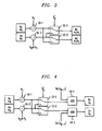
- FIG. 3 illustrates a basic selector structure for implementing the above-noted selection operation, i.e., the selection process for a QPSK modulation that leads to a complex multiplication according to the table of FIG. 2 and Equations (5) through (8) above.
- the basic selector structure includes inverters 10-1 and 10-2, and switches 12-1 and 12-2, interconnected as shown. As is apparent from FIG. 3 , the selection operation does not require any multiplication or addition. Instead, a two's complement logic is assumed as well as some basic logic to control the selectors based on the values of bits b 0 and b 1 . In this selector structure, the inverters 10-1 and 10-2 are assumed to be active high.
- inversion is performed if the control signal value is "1" and the input signal is passed through without inversion when the control signal value is "0."
- the switches 12-1 and 12-2 are assumed to be connected to the upper position when the control signal value is “1,” and connected to the lower position when the control signal value is "0.”
- the FIG. 4 implementation includes the elements of the FIG.
- FIG. 5 implementation eliminates the inverters 10-1 and 10-2 of the FIG. 3 selector by incorporating two's complement operations into add/sub units 16-1 and 16-2. Thus, apart from the switches 12-1 and 12-2 and other supporting logic, only two add/sub units are required if the sum is to be computed recursively.
- the add/sub units 16-1 and 16-2 are assumed to perform the addition operation when the value of their corresponding control signal is "1".
- FIG. 6 shows a fully recursive structure that can perform a complete FIR operation in accordance with Equation (9) without requiring any additional hardware.
- the FIG. 6 structure corresponds to the FIG. 5 structure with the addition of feedback to supply the real and imaginary parts of s k -1 to the corresponding inputs of the add/sub units 16-1 and 16-2, respectively.
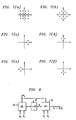
- FIG. 7(a) shows the 16-QAM constellation, with a set of 16 constellation points, u i ⁇ ⁇ 1 ⁇ j , ⁇ 1 ⁇ 3 j , ⁇ 3 ⁇ j , ⁇ 3 ⁇ 3 j ⁇ .
- the FIG. 7(a) constellation is rotated by 45°, resulting in the rotated constellation as shown in FIG. 7(b).
- FIGS. 7(c) through 7(f) show four different subsections of the rotated constellation of FIG. 7(b) .
- Each subsection in this example corresponds to a translated QPSK constellation.
- the center point of each subsection corresponds to a point in a rotated QPSK constellation.
- a first step involves the selection of the center point of a subsection, which is the same as selecting a point in a rotated QPSK constellation as described previously.
- the actual signal is selected. This is another selection process, similar to the previous selection. Note, however, that in the first step the value corresponding to the center point of each subsection is twice as large as the correction signal that is to be added. Thus, before the second step, a shift operation is required.
- the corresponding channel weight is now required to be selected as described in Equations (5) through (8) above, followed by a shift operation, and finally added by another selected value, as illustrated in FIG. 8 .
- the FIG. 8 structure includes a selector (SEL) 30, a left-shift (L-SH) element 32, and a recursive selector (REC) 34.
- the selector 30 in FIG. 8 corresponds to the selector shown in FIG. 3
- the recursive selector 34 corresponds to the recursive structure of FIGS. 4 or 5 .
- the left-shift element 30 implements the above-described left shift operation.
- FIG. 8 structure An example of the processing implemented by the FIG. 8 structure is as follows. Consider the constellation point (1 + 3 j ) in the conventional 16-QAM constellation, which is now mapped into (2 + j ) in the manner previously described. Note that the definition of one unit in actual implementation is arbitrary. In the first step, a multiply by 2 operation is performed using a selection operation implemented by selector 30, followed by a shift operation implemented by element 32. After that, the coefficient is multiplied by j , which is another selection operation. Finally, the two values obtained from the two steps are added together. This complex multiplication is implemented using two real add operations in the recursive selector 34.
- FIG. 9 shows the recursive structure for multiplying with a 64-QAM constellation point.
- the structure for the 64-QAM constellation requires a three stage recursion, and thus an additional left shift element 36 and recursive selector 38.
- the structures for larger constellations can be generated in a similar manner, as will be apparent to those skilled in the art.
- the operation in the first line is free, the second line costs two adds and so does the third and fourth.
- FIG. 10 shows a table comparing the number of operations required in an FIR filter implemented using the techniques of Section 1.1 with that of a conventional FIR filter, for different types of modulation.
- a conventional FIR filter with M complex valued coefficients requires 4 M real multiplications and (4 M - 2) real additions.
- the table of FIG. 10 shows the number of real add/sub operations required when applying the techniques of the invention. It can be seen from the table that, even for large constellations such as 1024-QAM, the techniques of the invention provide considerably lower complexity.
- FIG. 11 shows a possible implementation of an FIR filter chain using a concatenation of the 64-QAM blocks of FIG. 9 for multiplication.
- the concatenated 64-QAM blocks are denoted 40-1, 40-2, ... 40- M .
- the outputs of the blocks 40-1, 40-2, ... 40- M are combined in corresponding adders 42-1, 42-2, ... 42-( M -1).
- Another possible approach is to combine all first stages of the multiplication operations first, then the second and finally the third stages. This approach can save mantissa length and thus chip area. Typical values of M are around three to 64 while 1024-QAM or smaller constellations are typically used.
- a hierarchical tree structure can be used to reduce the delay from ( M - 1) T a to T a log 2 M , where T a is the delay time of one adder.
- T a is the delay time of one adder.
- the basic selector structure of FIG. 3 may be preferable, although now 2 two's complement inverters will generally be required for each coefficient, i.e., 2 M such inverters altogether. These two's complement inverters require not only cell area but also introduce a carry-ripple effect similar to that of standard adders, leading to an additional delay. Structures which avoid this additional delay will now be described with reference to FIGS. 12, 13 and 14 .
- either two add/sub structures or one add/sub with an additional inverter would generally be necessary. If, however, the sign signal is treated separately, just a pair of switches 50-1, 50-2 and one add/sub structure 52 is sufficient, as illustrated in FIG. 13 . This results in a savings in area as well as latency.
- the sign information, S ( A ) and S ( B ), for the two numbers, A and B has to be provided.
- the "wedge" operator ⁇ stands for the logical and function.
- FIG. 12 shows a table listing the four possible operations in terms of the sign operators and the outgoing signal Z . Furthermore, a multiplexer is required to select the correct input in case of a subtraction ( A - B , B - A ). The number Z is passed along together with its sign S ( Z ) to the following adder structure. The first stage only requires an additional selector for the coefficients. For adding two numbers A and B only the first operation A + B is required.
- FIG. 14 shows a first stage of an adder tree for a fast FIR filter implementation, illustrating this feature.
- the first stage of the tree includes switches 60-1, 60-2, 60-3 and 60-4, and add/sub units 62-1 and 62-2, interconnected as shown.
- Another advantage of treating the sign separately is that the sign information can be passed along to the next add/sub stage in the adder tree and can thus be incorporated in a subsequent add operation without the need for additional inverters.
- the sign information can be passed along to the next add/sub stage in the adder tree and can thus be incorporated in a subsequent add operation without the need for additional inverters.
- At the end of the tree structure one inverter might be necessary to provide final correction for the sign. It will be shown in the following section that the LMS algorithm can use this sign information immediately so that even this final inverter is not required.
- the adder tree comprises add/sub structures as shown in FIG. 13 , and the first stage can combine the selection of the coefficients and the add operations.
- FIG. 14 structure which assumes that two complex coefficients A R + jA 1 , and B R + jB 1 are QPSK modulated by the corresponding bits ⁇ a 0 , a 1 ⁇ and ⁇ b 0 , b 1 ⁇ .
- S Z I a 1 ⁇ b 1
- Subsequent adder stages are constructed in a straightforward manner in accordance with Equations 15 and 16.
- FIG. 15 is a table showing the complexity and minimum latency of the LMS algorithm, as implemented using the techniques of the invention, for different modulation techniques.
- a QPSK constellation requires 2 M add/sub operations to evaluate the error equation as well as updating the coefficient.
- the error computation requires 4M add/sub operations
- the multiplication e i ⁇ u i * requires 2 M add/sub operations
- the coefficient update requires 2 M add/sub operations, i.e., 8 M add/sub operations are required altogether.
- 4 M , 8 M and 12 M add/sub operations are required for QPSK, 16-QAM and 64-QAM constellations, respectively.
- the constellation size is increased by four times, another 4 M additional operations are required.
- FIG. 16 shows an exemplary implementation of this type, comprising add/sub units 70-1 and 70-2, selectors 72-1 through 72-4, and an add/sub hierarchical tree structure 74.
- the last inverter can be incorporated into the selection process of the coefficient update, i.e., if the negative information is active, - ⁇ e ( i ) is applied rather than ⁇ e ( i ) .
- the modified selection is faster because it is realized by simple logical gates and does not require an adder structure.
- one complete update cycle requires T a log 2 M for the FIR error part, possibly one T a for the error to multiply by the step-size ⁇ , and finally one add operation for the updates of the coefficients.
- the minimum update time is given by (log 2 M + 2) T a . If the step-size ⁇ is a negative power of two, the multiplication by the error is a simple scaling operation and can therefore be realized without any additional time delay.
- This operation gives a wide range for possible step-size values.
- the possible additional operation is indicated with a dashed box 75 in FIG. 16 .
- the whole update for a BPSK/QPSK training sequence can be performed in 6ns with add/sub operations while it takes about 12 ns when using multipliers.
- the optimum detector is a maximum-likelihood symbol sequence detector (MLSD), as described in, e.g., J.G. Proakis, "Channel equalization,” The Communications Handbook, CRC Press, 1997, Chapter 26 ; and G.D. Forney, Jr., "Maximum-likelihood sequence detection in the presence of intersymbol interference,” IEEE Trans. on Information Theory, Vol. IT-18, pp. 363-378, May 1972 .
- MLSD maximum-likelihood symbol sequence detector
- the Viterbi algorithm is modeled as a Finite-State Machine (FSM), called a trellis, with P M -1 states.
- FSM Finite-State Machine
- P the information symbol alphabet size
- M the number of complex-valued channel FIR filter coefficients, w l .
- FSM Finite-State Machine
- the values associated with the transitions between the states are w l u ( k ), i.e., the possible received values, given the estimated channel coefficients w l .
- FIG. 17 shows a table comparing the complexity for initialization (O( PM )) of the Section 1.1 and Section 1.2 implementations with a conventional implementation, for different types of modulation.
- O ( MP M ) In order to obtain the complete complexity of the Viterbi algorithm, O ( MP M ) needs to be added if a full search through the trellis is applied. This part can easily exceed the initial complexity of O ( PM ).
- Reduced complexity techniques may be applied, such as reduced-state sequence estimation techniques that limit the search through the trellis, as described in, e.g., M. Eyuboglu and S. Qureshi, "Reduced-state sequence estimation for coded modulation on intersymbol interference channels," IEEE Journal on Selected Areas in Communications, Vol. 7, pp. 989-995, August 1989 .
- the initial complexity can become very significant.
- Using a tree structure in accordance with the invention for implementing the add operations can further reduce the complexity as described in Section 1.1 above.
- FIG. 18 shows an illustrative embodiment of a receiver 100 in which the above-described signal processing operations may be implemented.
- the receiver 100 receives a sequence of symbols transmitted by a transmitter 102. The symbols are generated by transmitter 102 in accordance with a rotated constellation as previously described.
- the receiver 100 includes a ML sequence detector (MLSD) 104 which implements the Viterbi algorithm, and is connected in parallel with an LMS estimator 106.
- MLSD ML sequence detector
- LMS estimator 106 One or both of the MLSD 104 and LMS estimator 106 are implemented using the computational techniques described above.
- the channel estimates from the LMS estimator 106 are fed to the MLSD as shown.
- An optional channel decoder 108 is also included in the receiver 100.
- FIG. 19 shows another example receiver 120 in which the invention may be implemented.
- the receiver 120 which implements a decision feedback equalization (DFE) technique, and includes the MLSD 104, LMS estimator 106 and optional channel decoder 108, and also includes a set of feed-forward filters 122 and a set of feedback filters 124.
- the output of the LMS estimator in this case is used to determine adaptive filter taps for the set of feedback filters 124.
- the received symbols are processed through feed-forward filters 122, and then applied to the MLSD 104.
- the output of the MLSD is fedback through the feedback filters 124.
- FIGS. 18 and 19 are examples only, and other embodiments may include different arrangements of elements and/or additional elements not explicitly shown.
- the invention provides efficient computational methods and apparatus that allow large reductions in complexity for implementations of communication algorithms that require multiplying a coefficient with a constellation point in a PSK or QAM constellation. Chip area as well as latency can be reduced due to the substitution of multiplications by simpler functions. Note that applying this technique does not cause any approximation or reduction in precision, but simply removes area-intensive and time-intensive operations.
- FIGS. 3-6 , 8 , 9, 11 , 13, 14 and 16 may be implemented as elements of an application-specific integrated circuit (ASIC) or other digital data processing device for use in a channel estimator, channel equalizer, demodulator, decoder or other element of a digital communication system receiver.
- ASIC application-specific integrated circuit
Landscapes
- Engineering & Computer Science (AREA)
- Computer Networks & Wireless Communication (AREA)
- Signal Processing (AREA)
- Digital Transmission Methods That Use Modulated Carrier Waves (AREA)
- Cable Transmission Systems, Equalization Of Radio And Reduction Of Echo (AREA)
- Error Detection And Correction (AREA)
Claims (18)
- Procédé de traitement de l'information dans un récepteur (100 ; 120) d'un système de communication numérique, le procédé comprenant les étapes consistant à :appliquer une opération de traitement de signal à une séquence de symboles transmis, dans lequel les symboles transmis correspondent à des points dans une première constellation de modulation, la première constellation de modulation correspondant à une version entraînée en rotation d'une deuxième constellation de modulation, et chacun des symboles transmis représente un nombre particulier de bits d'information comprenant un premier bit d'information b0 et un deuxième bit d'information b1 ;l'opération de traitement du signal utilisant au moins un sélecteur (30) pour calculer un produit d'un élément d'une estimation de canal et un symbole donné des symboles transmis ;CARACTÉRISÉ EN CE QUE le sélecteur comprend un premier et un deuxième inverseur contrôlable (10-1, 10-2) et un premier et un deuxième commutateur (12-1, 12-2), les premier et deuxième inverseurs étant adaptés pour recevoir des parties réelle et imaginaires respectives de l'élément de l'estimation de canal, ledit inverseur contrôlable inversant ou n'inversant pas la partie réelle sur la base d'un premier signal de commande, le premier signal de commande étant déterminé par b1, ledit deuxième inverseur contrôlable inversant ou n'inversant pas la partie imaginaire sur la base d'un deuxième signal de commande, le deuxième signal de commande étant déterminé par à la fois b0 et b1, dans lequel chacun des premier et deuxième commutateurs a une entrée adaptée pour recevoir la partie réelle inversée ou non inversée depuis le premier inverseur contrôlable et une autre entrée adaptée pour recevoir la partie imaginaire inversée ou non inversée depuis le deuxième inverseur contrôlable, chacun des premier et deuxième commutateurs étant capable de sélectionner comme sa sortie l'une de ses deux entrées qui réagit à un troisième signal de commande, le troisième signal de commande étant déterminé par b0, dans lequel les sorties des premier et deuxième commutateurs fournissent des parties réelle et imaginaire respectives d'un produit de l'élément de l'estimation de canal et le symbole donné.
- Procédé selon la revendication 1, dans lequel l'utilisation de la première constellation de modulation permet à l'opération de traitement de signal d'être réalisée sans opérations de multiplication.
- Procédé selon la revendication 1, dans lequel la première constellation de modulation est générée par l'application d'une rotation de 45° à la deuxième constellation de modulation.
- Procédé selon la revendication 1, dans lequel la deuxième constellation de modulation comprend l'une d'une constellation PSK (de modulation par changement de phase) et d'une constellation QAM (de modulation d'amplitude en quadrature).
- Procédé selon la revendication 1, dans lequel l'opération de traitement de signal comprend au moins une opération de filtrage à réponse impulsionnelle finie, une opération d'estimation de la moyenne des moindres carrés (106) et une opération de détection de la séquence de maximum de vraisemblance (104) en utilisant un algorithme de Viterbi.
- Procédé selon la revendication 1, dans lequel le sélecteur comprend en outre une première et une deuxième unité d'addition (14-1, 14-2), les première et deuxième unités d'addition calculant les éléments des parties réelle et imaginaire respectives d'un produit vectoriel interne.
- Procédé selon la revendication 6, dans lequel une opération de filtrage à réponse impulsionnelle finie est réalisée en utilisant le sélecteur en incluant la rétroaction des sorties des unités d'addition à des entrées correspondantes des unités d'addition.
- Procédé selon la revendication 1, dans lequel l'opération de traitement de signal comprend une opération de multiplication à plusieurs étages réalisée sans opérations de multiplication, dans laquelle chaque étage de l'opération à plusieurs étages correspond à un sélecteur, et un élément de décalage à gauche (32 ; 36) est prévu entre une sortie d'un étage donné des étages (30 ; 34) et une entrée correspondante d'un étage ultérieur (34 ; 38).
- Procédé de la revendication 1, dans lequel l'opération de traitement de signal est mise en oeuvre en utilisant un arbre d'addition hiérarchique à plusieurs étages (42) sans opérations de multiplication.
- Appareil de traitement de l'information pour utilisation dans un récepteur (100 ; 120) d'un système de communication numérique, l'appareil comprenant :un circuit de traitement de signal pour le traitement d'une séquence de symboles transmis, dans lequel les symboles transmis correspondent à des points dans une première constellation de modulation, la première constellation de modulation correspondant à une version entraînée en rotation d'une deuxième constellation de modulation, et chacun des symboles transmis représente un nombre particulier de bits d'information comprenant un premier bit d'information b0 et un deuxième bit d'information b1 ;le circuit de traitement de signal comprend au moins un sélecteur (30) configuré pour calculer un produit d'un élément d'une estimation de canal et un symbole donné des symboles transmis ;CARACTÉRISÉ EN CE QUE le sélecteur comprend un premier et un deuxième inverseur contrôlable (10-1, 10-2) et un premier et un deuxième commutateur (12-1, 12-2), les premier et deuxième inverseurs contrôlables étant adaptés pour recevoir des parties réelle et imaginaire respectives de l'élément de l'estimation de canal, ledit premier inverseur contrôlable inversant ou n'inversant pas la partie réelle sur la base d'un premier signal de commande, le premier signal de commande étant déterminé par b1, ledit deuxième inverseur contrôlable inversant ou n'inversant pas la partie imaginaire sur la base d'un deuxième signal de commande, le deuxième signal de commande étant déterminé par à la fois b0 et b1, dans lequel chacun des premier et deuxième commutateurs est doté d'une entrée adaptée pour recevoir la partie réelle inversée ou non inversée depuis le premier inverseur contrôlable et une autre entrée adaptée pour recevoir la partie imaginaire inversée ou non inversée depuis le deuxième inverseur contrôlable, chacun des premier et deuxième commutateurs étant capable de sélectionner comme sa sortie l'une de ses deux entrées qui réagit à un troisième signal de commande, le troisième signal de commande étant déterminé par b0, dans lequel les sorties des premier et deuxième commutateurs fournissent des parties réelle et imaginaire respectives de l'élément de l'estimation de canal et du symbole donné.
- Appareil selon la revendication 10, dans lequel l'utilisation de la première constellation de modulation permet à l'opération de traitement de signal d'être réalisée sans opérations de multiplication.
- Appareil selon la revendication 10, dans lequel la première constellation de modulation est générée par l'application d'une rotation de 45° à la deuxième constellation de modulation.
- Appareil selon la revendication 10, dans lequel l'autre constellation de modulation comprend l'une d'une constellation PSK et d'une constellation QAM.
- Appareil selon la revendication 10, dans lequel le circuit de traitement de signal comprend au moins un d'un filtre à réponse impulsionnelle finie, d'un estimateur de la moyenne des moindres carrés (106) et d'un détecteur de séquence de maximum de vraisemblance (104) mis en oeuvre en utilisant un algorithme de Viterbi.
- Appareil selon la revendication 10, dans lequel le sélecteur comprend en outre une première et une deuxième unité d'addition (14-1, 14-2), les première et deuxième unités d'addition calculant les éléments des parties réelle et imaginaire respectives d'un produit vectoriel interne.
- Appareil selon la revendication 10, dans lequel le circuit de traitement de signal comprend un circuit à plusieurs étages mis en oeuvre sans opérations de multiplication, dans lequel chaque étage du circuit à plusieurs étages correspond à un sélecteur et un élément de décalage à gauche (32 ; 36) est prévu entre une sortie d'un étage donné des étages (30 ; 34) et une entrée correspondante d'un étage ultérieur (34 ; 38).
- Appareil selon la revendication 10, dans lequel le circuit de traitement de signal est mis en oeuvre en utilisant un arbre additionneur hiérarchique à plusieurs étages (42) sans opérations de multiplication.
- Système de communication numérique, comprenant :un transmetteur (102) pour générer une séquence de symboles transmis, dans lequel les symboles transmis correspondent à des points dans une première constellation de modulation générée par l'application d'une rotation prédéterminée à une deuxième constellation de modulation, et chacun des symboles transmis représente un nombre particulier de bits d'information comprenant un premier bit d'information b0 et un deuxième bit d'information b1 ; etun récepteur (100) pour appliquer une opération de traitement de signal à la séquence de symboles transmis ;l'opération de traitement de signal utilisant au moins un sélecteur (30) configuré pour calculer un produit d'un élément d'estimation de canal et un symbole donné des symboles transmis ;CARACTÉRISÉ EN CE QUE le sélecteur comprend un premier et un deuxième inverseur contrôlable (10.1, 10.2) et un premier et un deuxième commutateur (12-1, 12-2), les premier et deuxième inverseurs contrôlables étant adaptés pour recevoir des parties réelle et imaginaire respectives de l'élément de l'estimation de canal, ledit premier inverseur contrôlable inversant ou n'inversant pas la partie réelle sur la base d'un premier signal de commande, le premier signal de commande étant déterminé par b1, ledit deuxième inverseur contrôlable inversant ou n'inversant pas la partie imaginaire sur la base d'un deuxième signal de commande, le deuxième signal de commande étant déterminé par à la fois b0 et b1. dans lequel chacun des premier et deuxième commutateurs a une entrée adaptée pour recevoir la partie réelle inversée ou non inversée depuis le premier inverseur contrôlable et une autre entrée adaptée pour recevoir la partie imaginaire inversée ou non inversée depuis le deuxième inverseur contrôlable, chacun des premier et deuxième commutateurs étant capable de sélectionner comme sa sortie l'une de ses deux entrées qui réagit à un troisième signal de commande, le troisième signal de commande étant déterminé par b0, dans lequel les sorties du premier et du deuxième commutateur fournissent des parties réelle et imaginaire respectives d'un produit de l'estimation de canal et le symbole donné.
Applications Claiming Priority (2)
| Application Number | Priority Date | Filing Date | Title |
|---|---|---|---|
| US390389 | 1995-02-16 | ||
| US09/390,389 US6914934B1 (en) | 1999-09-03 | 1999-09-03 | Multiplier-free methods and apparatus for signal processing in a digital communication system |
Publications (3)
| Publication Number | Publication Date |
|---|---|
| EP1081908A2 EP1081908A2 (fr) | 2001-03-07 |
| EP1081908A3 EP1081908A3 (fr) | 2002-09-18 |
| EP1081908B1 true EP1081908B1 (fr) | 2014-02-19 |
Family
ID=23542290
Family Applications (1)
| Application Number | Title | Priority Date | Filing Date |
|---|---|---|---|
| EP00307409.3A Expired - Lifetime EP1081908B1 (fr) | 1999-09-03 | 2000-08-29 | Traitement de signal sans multiplications dans des récepteurs pour signaux numériques |
Country Status (3)
| Country | Link |
|---|---|
| US (1) | US6914934B1 (fr) |
| EP (1) | EP1081908B1 (fr) |
| JP (2) | JP4397515B2 (fr) |
Cited By (1)
| Publication number | Priority date | Publication date | Assignee | Title |
|---|---|---|---|---|
| WO2015157733A1 (fr) * | 2014-04-11 | 2015-10-15 | Futurewei Technologies, Inc. | Procédé et système pour réaliser une compensation de non-linéarité de fibre pour une modulation d'amplitude en qam16 optique |
Families Citing this family (11)
| Publication number | Priority date | Publication date | Assignee | Title |
|---|---|---|---|---|
| US20020150155A1 (en) * | 2001-02-26 | 2002-10-17 | Itzhak Florentin | Convergence speed, lowering the excess noise and power consumption of equalizers |
| DE10210234B4 (de) * | 2002-03-08 | 2011-02-03 | Advanced Micro Devices, Inc., Sunnyvale | LMS-basierte Kanalschätzung |
| US7184488B2 (en) * | 2002-03-15 | 2007-02-27 | Lucent Technologies Inc. | Quasi-orthogonal space-time codes |
| US7483933B2 (en) * | 2005-02-17 | 2009-01-27 | Samsung Electronics Co., Ltd. | Correlation architecture for use in software-defined radio systems |
| US7864832B2 (en) * | 2005-05-06 | 2011-01-04 | Samsung Electronics Co., Ltd. | Multi-code correlation architecture for use in software-defined radio systems |
| CN101558620B (zh) * | 2006-05-19 | 2014-11-12 | Lg电子株式会社 | 利用和操控无线资源以便高效且有效地进行无线通信的方法 |
| US8135058B2 (en) | 2008-10-10 | 2012-03-13 | Csr Technology Inc. | Adaptive known signal canceller |
| JP5221480B2 (ja) * | 2009-09-08 | 2013-06-26 | 株式会社東芝 | 直交変調器、および送信装置 |
| US9787408B2 (en) * | 2015-10-06 | 2017-10-10 | Huawei Technologies Co., Ltd. | Apparatus and method for unified mitigation of correlative additive and multiplicative noise |
| EP3217554B1 (fr) * | 2016-03-11 | 2019-10-02 | Intel IP Corporation | Appareils et procédés permettant de compenser les fluctuations de phase |
| US20250105943A1 (en) * | 2023-09-21 | 2025-03-27 | Microchip Technology Incorporated | Reducing startup time of a trellis-based mlse decoder |
Family Cites Families (10)
| Publication number | Priority date | Publication date | Assignee | Title |
|---|---|---|---|---|
| US4381546A (en) | 1979-03-02 | 1983-04-26 | Paradyne Corporation | System for the quantitative measurement of impairments in the communication channel of a quadrature amplitude modulation data communication system |
| US4520490A (en) * | 1983-08-05 | 1985-05-28 | At&T Information Systems Inc. | Differentially nonlinear convolutional channel coding with expanded set of signalling alphabets |
| US5289501A (en) * | 1991-11-26 | 1994-02-22 | At&T Bell Laboratories | Coded modulation with unequal error protection for fading channels |
| JPH06112983A (ja) * | 1992-09-25 | 1994-04-22 | Kokusai Electric Co Ltd | フレーム同期回路 |
| JPH1127156A (ja) * | 1997-07-07 | 1999-01-29 | Matsushita Electric Ind Co Ltd | 誤り訂正復号装置 |
| JP3209157B2 (ja) * | 1997-09-09 | 2001-09-17 | 松下電器産業株式会社 | ピーク制御装置 |
| US6233271B1 (en) * | 1997-12-31 | 2001-05-15 | Sony Corporation | Method and apparatus for decoding trellis coded direct sequence spread spectrum communication signals |
| JPH11220505A (ja) * | 1998-01-30 | 1999-08-10 | Matsushita Electric Ind Co Ltd | 変調方式とそれを用いた無線通信システム |
| JP2000216711A (ja) * | 1999-01-21 | 2000-08-04 | Matsushita Electric Ind Co Ltd | 無線受信装置及び信号処理方法 |
| US6611567B1 (en) * | 1999-01-29 | 2003-08-26 | Agere Systems, Inc. | Method and apparatus for pulse shaping |
-
1999
- 1999-09-03 US US09/390,389 patent/US6914934B1/en not_active Expired - Fee Related
-
2000
- 2000-08-29 EP EP00307409.3A patent/EP1081908B1/fr not_active Expired - Lifetime
- 2000-09-01 JP JP2000264844A patent/JP4397515B2/ja not_active Expired - Fee Related
-
2009
- 2009-07-03 JP JP2009158459A patent/JP2009232476A/ja not_active Ceased
Cited By (1)
| Publication number | Priority date | Publication date | Assignee | Title |
|---|---|---|---|---|
| WO2015157733A1 (fr) * | 2014-04-11 | 2015-10-15 | Futurewei Technologies, Inc. | Procédé et système pour réaliser une compensation de non-linéarité de fibre pour une modulation d'amplitude en qam16 optique |
Also Published As
| Publication number | Publication date |
|---|---|
| JP4397515B2 (ja) | 2010-01-13 |
| JP2009232476A (ja) | 2009-10-08 |
| US6914934B1 (en) | 2005-07-05 |
| EP1081908A3 (fr) | 2002-09-18 |
| EP1081908A2 (fr) | 2001-03-07 |
| JP2001160768A (ja) | 2001-06-12 |
Similar Documents
| Publication | Publication Date | Title |
|---|---|---|
| JP2009232476A (ja) | 情報処理方法および情報処理装置 | |
| KR100785410B1 (ko) | 하이브리드 서바이버 메모리 구조체 | |
| US5870433A (en) | Method of processing signals in a viterbi decoder according to delayed decision feedback sequence estimation (DDFSE) algorithm | |
| US4468786A (en) | Nonlinear equalizer for correcting intersymbol interference in a digital data transmission system | |
| US5471504A (en) | Bilinear decision feedback equalizer | |
| US5432816A (en) | System and method of robust sequence estimation in the presence of channel mismatch conditions | |
| US5214672A (en) | Trellis precoding for fractional bits/baud | |
| US6069917A (en) | Blind training of a decision feedback equalizer | |
| US6178209B1 (en) | Method of estimating trellis encoded symbols utilizing simplified trellis decoding | |
| EP1065851A1 (fr) | Egaliseur à décision récursive avec estimation de séquence à nombre d'états reduite | |
| US6269116B1 (en) | Method and arrangement for demodulating data symbols | |
| KR20010014993A (ko) | 계산 복잡도를 감소시키고 축소 상태 시퀀스 추정 기술의임계 경로를 릴랙싱하는 방법 및 장치 | |
| JPH10126315A (ja) | 通信受信機において使用するための方法および受信機において使用するための装置 | |
| EP0969640A2 (fr) | Récupération de phase avec égalisation aveugle pour récepteurs à modes CAP et MAQ | |
| US11438197B2 (en) | Adaptive equalizer with a real feedforward filter and a single complex feedforward tap | |
| JP2000036777A (ja) | 定数モジュラス・アルゴリズムとマルチモジュラス・アルゴリズムの両方を使用するブラインド形等化アルゴリズム | |
| JP7200363B2 (ja) | 狭帯域フィルタ済み信号のためのノイズホワイトニング後補償の効率的実施 | |
| US5892801A (en) | Decision path reduction of M-ary tree-search detector | |
| EP0969635B1 (fr) | Egalisation aveugle dans des récepteurs à modes CAP et MAQ | |
| JP2001525139A (ja) | 周波数選択デジタル伝送チャネルの等化及び復号装置 | |
| Rupp et al. | On efficient multiplier-free implementation of channel estimation and equalization | |
| Si-yuan et al. | A computationally efficient multi-modulus blind equalization algorithm | |
| Larsson | Adaptive phase shifting in FIR filters with application to equalizers | |
| YANG et al. | Low complexity adaptive blind equalization using the frequency domain block constant modulus algorithm | |
| Sheen | Performance analysis of sequence estimation techniques for intersymbol interference channels |
Legal Events
| Date | Code | Title | Description |
|---|---|---|---|
| PUAI | Public reference made under article 153(3) epc to a published international application that has entered the european phase |
Free format text: ORIGINAL CODE: 0009012 |
|
| AK | Designated contracting states |
Kind code of ref document: A2 Designated state(s): AT BE CH CY DE DK ES FI FR GB GR IE IT LI LU MC NL PT SE |
|
| AX | Request for extension of the european patent |
Free format text: AL;LT;LV;MK;RO;SI |
|
| PUAL | Search report despatched |
Free format text: ORIGINAL CODE: 0009013 |
|
| AK | Designated contracting states |
Kind code of ref document: A3 Designated state(s): AT BE CH CY DE DK ES FI FR GB GR IE IT LI LU MC NL PT SE |
|
| AX | Request for extension of the european patent |
Free format text: AL;LT;LV;MK;RO;SI |
|
| 17P | Request for examination filed |
Effective date: 20030318 |
|
| AKX | Designation fees paid |
Designated state(s): DE FR GB |
|
| 17Q | First examination report despatched |
Effective date: 20040301 |
|
| 17Q | First examination report despatched |
Effective date: 20040301 |
|
| APBK | Appeal reference recorded |
Free format text: ORIGINAL CODE: EPIDOSNREFNE |
|
| APBN | Date of receipt of notice of appeal recorded |
Free format text: ORIGINAL CODE: EPIDOSNNOA2E |
|
| APBR | Date of receipt of statement of grounds of appeal recorded |
Free format text: ORIGINAL CODE: EPIDOSNNOA3E |
|
| APAF | Appeal reference modified |
Free format text: ORIGINAL CODE: EPIDOSCREFNE |
|
| RAP3 | Party data changed (applicant data changed or rights of an application transferred) |
Owner name: LUCENT TECHNOLOGIES INC. |
|
| APBT | Appeal procedure closed |
Free format text: ORIGINAL CODE: EPIDOSNNOA9E |
|
| GRAP | Despatch of communication of intention to grant a patent |
Free format text: ORIGINAL CODE: EPIDOSNIGR1 |
|
| RAP1 | Party data changed (applicant data changed or rights of an application transferred) |
Owner name: ALCATEL-LUCENT USA INC. |
|
| RAP1 | Party data changed (applicant data changed or rights of an application transferred) |
Owner name: LUCENT TECHNOLOGIES INC. |
|
| GRAS | Grant fee paid |
Free format text: ORIGINAL CODE: EPIDOSNIGR3 |
|
| GRAA | (expected) grant |
Free format text: ORIGINAL CODE: 0009210 |
|
| AK | Designated contracting states |
Kind code of ref document: B1 Designated state(s): DE FR GB |
|
| REG | Reference to a national code |
Ref country code: GB Ref legal event code: FG4D |
|
| REG | Reference to a national code |
Ref country code: DE Ref legal event code: R096 Ref document number: 60048434 Country of ref document: DE Effective date: 20140327 |
|
| PGFP | Annual fee paid to national office [announced via postgrant information from national office to epo] |
Ref country code: DE Payment date: 20140827 Year of fee payment: 15 |
|
| REG | Reference to a national code |
Ref country code: DE Ref legal event code: R097 Ref document number: 60048434 Country of ref document: DE |
|
| PGFP | Annual fee paid to national office [announced via postgrant information from national office to epo] |
Ref country code: GB Payment date: 20140827 Year of fee payment: 15 |
|
| PLBE | No opposition filed within time limit |
Free format text: ORIGINAL CODE: 0009261 |
|
| STAA | Information on the status of an ep patent application or granted ep patent |
Free format text: STATUS: NO OPPOSITION FILED WITHIN TIME LIMIT |
|
| 26N | No opposition filed |
Effective date: 20141120 |
|
| REG | Reference to a national code |
Ref country code: DE Ref legal event code: R097 Ref document number: 60048434 Country of ref document: DE Effective date: 20141120 |
|
| REG | Reference to a national code |
Ref country code: FR Ref legal event code: ST Effective date: 20150430 |
|
| PG25 | Lapsed in a contracting state [announced via postgrant information from national office to epo] |
Ref country code: FR Free format text: LAPSE BECAUSE OF NON-PAYMENT OF DUE FEES Effective date: 20140901 |
|
| REG | Reference to a national code |
Ref country code: DE Ref legal event code: R119 Ref document number: 60048434 Country of ref document: DE |
|
| GBPC | Gb: european patent ceased through non-payment of renewal fee |
Effective date: 20150829 |
|
| PG25 | Lapsed in a contracting state [announced via postgrant information from national office to epo] |
Ref country code: DE Free format text: LAPSE BECAUSE OF NON-PAYMENT OF DUE FEES Effective date: 20160301 Ref country code: GB Free format text: LAPSE BECAUSE OF NON-PAYMENT OF DUE FEES Effective date: 20150829 |
|
| REG | Reference to a national code |
Ref country code: DE Ref legal event code: R082 Ref document number: 60048434 Country of ref document: DE Representative=s name: DILG, HAEUSLER, SCHINDELMANN PATENTANWALTSGESE, DE Ref country code: DE Ref legal event code: R082 Ref document number: 60048434 Country of ref document: DE Representative=s name: DILG HAEUSLER SCHINDELMANN PATENTANWALTSGESELL, DE Ref country code: DE Ref legal event code: R081 Ref document number: 60048434 Country of ref document: DE Owner name: AVAGO TECHNOLOGIES GENERAL IP (SINGAPORE) PTE., SG Free format text: FORMER OWNER: LUCENT TECHNOLOGIES, INC., MURRAY HILL, N.J., US |