EP1069437B1 - Procede de commande de manipulation d'ic, systeme de commande dans lequel ledit procede est utilise - Google Patents
Procede de commande de manipulation d'ic, systeme de commande dans lequel ledit procede est utilise Download PDFInfo
- Publication number
- EP1069437B1 EP1069437B1 EP99962509A EP99962509A EP1069437B1 EP 1069437 B1 EP1069437 B1 EP 1069437B1 EP 99962509 A EP99962509 A EP 99962509A EP 99962509 A EP99962509 A EP 99962509A EP 1069437 B1 EP1069437 B1 EP 1069437B1
- Authority
- EP
- European Patent Office
- Prior art keywords
- socket
- test hand
- pusher
- displacement
- test
- Prior art date
- Legal status (The legal status is an assumption and is not a legal conclusion. Google has not performed a legal analysis and makes no representation as to the accuracy of the status listed.)
- Expired - Lifetime
Links
Images
Classifications
-
- H10P72/00—
-
- G—PHYSICS
- G01—MEASURING; TESTING
- G01R—MEASURING ELECTRIC VARIABLES; MEASURING MAGNETIC VARIABLES
- G01R31/00—Arrangements for testing electric properties; Arrangements for locating electric faults; Arrangements for electrical testing characterised by what is being tested not provided for elsewhere
- G01R31/28—Testing of electronic circuits, e.g. by signal tracer
- G01R31/2851—Testing of integrated circuits [IC]
- G01R31/2893—Handling, conveying or loading, e.g. belts, boats, vacuum fingers
-
- G—PHYSICS
- G01—MEASURING; TESTING
- G01R—MEASURING ELECTRIC VARIABLES; MEASURING MAGNETIC VARIABLES
- G01R31/00—Arrangements for testing electric properties; Arrangements for locating electric faults; Arrangements for electrical testing characterised by what is being tested not provided for elsewhere
- G01R31/26—Testing of individual semiconductor devices
-
- G—PHYSICS
- G01—MEASURING; TESTING
- G01R—MEASURING ELECTRIC VARIABLES; MEASURING MAGNETIC VARIABLES
- G01R31/00—Arrangements for testing electric properties; Arrangements for locating electric faults; Arrangements for electrical testing characterised by what is being tested not provided for elsewhere
- G01R31/28—Testing of electronic circuits, e.g. by signal tracer
- G01R31/2851—Testing of integrated circuits [IC]
- G01R31/2886—Features relating to contacting the IC under test, e.g. probe heads; chucks
- G01R31/2887—Features relating to contacting the IC under test, e.g. probe heads; chucks involving moving the probe head or the IC under test; docking stations
-
- G—PHYSICS
- G01—MEASURING; TESTING
- G01R—MEASURING ELECTRIC VARIABLES; MEASURING MAGNETIC VARIABLES
- G01R31/00—Arrangements for testing electric properties; Arrangements for locating electric faults; Arrangements for electrical testing characterised by what is being tested not provided for elsewhere
- G01R31/28—Testing of electronic circuits, e.g. by signal tracer
- G01R31/2851—Testing of integrated circuits [IC]
- G01R31/2886—Features relating to contacting the IC under test, e.g. probe heads; chucks
- G01R31/2891—Features relating to contacting the IC under test, e.g. probe heads; chucks related to sensing or controlling of force, position, temperature
-
- G—PHYSICS
- G01—MEASURING; TESTING
- G01R—MEASURING ELECTRIC VARIABLES; MEASURING MAGNETIC VARIABLES
- G01R31/00—Arrangements for testing electric properties; Arrangements for locating electric faults; Arrangements for electrical testing characterised by what is being tested not provided for elsewhere
- G01R31/28—Testing of electronic circuits, e.g. by signal tracer
- G01R31/2851—Testing of integrated circuits [IC]
Definitions
- This invention relates to a method of controlling the operation of a test hand for pressing down an IC device (hereinafter, referred to as an IC) properly on a socket according to the types of the IC and socket in an IC handler used for a semiconductor tester, a recording instrument and a controlling/operating system.
- an IC IC device
- An IC handler has been in common use as a semiconductor tester.
- an IC transferred from the IC loader is placed on the socket of the measuring section.
- the pusher of the test hand presses the IC against the socket to bring the contact section of the IC, such as the lead pins, into contact with the contactor of the socket.
- the tester judges whether the IC characteristic is acceptable. Then, the unloader separates the IC from a reject and holds it.
- the types of ICs to be tested have been diversified and consequently the types of sockets to hold them have also been diversified.
- the operating performance of the test hand should be changed so as to deal with the type of IC. Since the semiconductor tester is requested to process many ICs in a short time, it is desirable that the IC handler should function at high speed. However, the faster the processing speed becomes, the more increase the impact of the pusher on the IC when the pusher is pressed against the IC, and thus the service life of the lead pins of the IC and the socket contactor may become shorter.
- Jpn. Pat. Appln. KOKAI Publication No. 10-227834 has disclosed a mechanism for making fine adjustments to the proper pressure, speed, and displacement of IC pressed into a socket according to the type of IC.
- the IC is pressed down by the test hand as it is in a socket, it may not be assured that the values based on the specified data items are always proper. For example, as the working speed of the test hand is increased to process the IC at high speed, the impact on the IC happens and becomes larger when the test hand hits the IC package. In addition, the impact force is likely to exceed the material strength of the IC leads or socket contactor and do damage to the IC package.
- US 5 285 946 discloses an apparatus for mounting electronic components on the surface of printed boards by a suction head assembly coupled to a head lift mechanism comprising a force sensor for measuring the pressure exerted on the component by a mounting operation, and a microcomputer for preparing a control signal in accordance with the deviation of the value measured by the force sensor from a desired value of pressure on the component.
- US 5 568 032 discloses a position control system which includes a plurality of actuators for moving an object, a plurality of sensors for detecting the state of the object, a first circuit for extracting a state signal, in each of different kinetic modes related to the object, from outputs of the sensors, a compensating circuit for compensating for the state signals in the respective kinetic modes, a second circuit for distributing an output of the compensating circuit and for providing drive signals for the actuators in accordance therewith, and a driver for driving the actuators in response to the drive signals.
- US 5 818 247 discloses a method and an apparatus for testing an internal circuit reducing working hours and production costs for an electronic product using a multi-fixture.
- the present invention is to provide an operation method and system for an IC handler to control properly the pushing pressure, operating speed and displacement of the test hand according to the types of IC and socket.
- the operating method of the working of test hand to control appropriately the pushing force, operating velocity and displacement thereof in the IC handler is invented.
- the control method of the test hand for pushing the contact of the IC on the socket of the IC handler comprises the step of measuring data by means of sensors through the trial to press an IC on the socket repeatedly by the test hand, so as to obtain data representing the load, the acceleration or velocity, and the amount of thrusting displacement of the test hand until the stoppage thereof after the tip of the test hand contacts with the IC; obtaining the combined spring constant K of the IC socket; and determining the motion of test hand so as to work the impact force to an IC becoming smaller than the allowable press force.
- a control system of the present invention comprises a load sensor for detecting the press force of the test hand applied to an IC; an acceleration sensor for detecting the operating velocity or acceleration of the test hand; a displacement sensor for measuring the thrusting displacement during the time from when the test hand comes into contact with the IC until it stops; and control means for not only calculating the combined spring constant for the IC and a socket on the basis of the data items from the individual sensors, but also controlling the driving of the test hand on the basis of the individual data items so that the press force, velocity, and displacement may reach such values that make the impact force acting on the IC equal to or smaller than an allowed value and speed up the operation of the test hand to the maximum.
- FIG. 1 is a block diagram showing the overall configuration of a control system for the test hand in an IC handler according to an embodiment of the present invention.
- FIG. 1 schematically shows an IC test section composed of a pulse motor 3, a driving circuit 17, a test hand 1, a pusher 8 provided on a support plate F1, an IC 5, a contactor 4, and a socket 2.
- a load sensor 9 using a strain gauge load transducer and a strain gauge accelerometer 10 are provided between frames F2 and F3.
- a noncontacting displacement sensor 11 using an eddy-current displacement measuring device is provided on a frame F4 that supports the socket 2.
- a lightweight, rigid aluminum arm 7 to hold a target 6 of the displacement sensor 11 is provided above the pusher 8.
- FIG. 1 shows a system for collecting and processing the electric signals sent by the sensors 9 to 11.
- the control system is composed of an amplifier 12, an A/D converter 13, a computer 14, and a D/A converter 16.
- the electrical signals are digitized by the A/D converter and then the arithmetic process is executed by a computer.
- a control signal is sent to the driving circuit 17. Detailed explanation will be given below.
- the pulse motor 3 is fixed on the top end of test hand body 1.
- the pusher 8 is provided in such a manner that it can move up and down freely.
- a suction hole 20 for causing the IC 5 to adhere to the tip by suction at air pressure is made.
- the suction hole 20 is connected to a compressor 21 via an air hole made inside the pusher 8 and test hand body 1.
- the support plate F1 is joined to the pulse motor 3 and the pusher 8 is fixed onto the support plate F2 via a load sensor 9 and a frame F3, the pusher 8 and support plates F2, F3 are moved up and down as one piece by the pulse motor 3.
- the socket 2 on the frame F4 is provided below the pusher 8.
- the contactor 4 is provided at the IC acceptor of the socket 2 so that it may touch the contacts of the IC 5, such as the leads.
- the acceleration sensor 10 is provided onto the lower frame F3 of the pair of frames F2, F3.
- the test hand 1 has the pusher 8 at its lower end. Adhering the IC 5 by suction at its tip, the pusher 8 is moved up and down by the pulse motor 3.
- the test hand 1 can adjust the pushing pressure on the IC 5 and socket 2, the working speed, and the thrusting displacement of IC by controlling the number of revolutions and rotational speed of the pulse motor 3. As described later, the test hand 1 is designed to be decelerated just before the tip of the pusher 8 comes into contact with the socket 2 so as to alleviate its impact on the IC 5 and socket 2.
- the load sensor 9 is for detecting the pushing pressure of the test hand 1, or the pusher 8, on the IC 5 and socket 2.
- the load sensor is provided between the frames F2 and F3.
- the acceleration sensor 10 is used for detecting the acceleration or a change of the velocity when the test hand 1 goes down.
- a strain gauge sensor or piezoelectric sensor can be used as the acceleration sensor 10.
- An acceleration sensor may be used in place of the velocity sensor. In this case, the velocity can be obtained by differentiating numerically the digitized data of displacement by means of the computer 14.
- the displacement sensor 11 is for measuring the displacement D from the position just before the IC 5 stuck by suction to the pusher 8 comes into contact with the contactor 4 of the socket 2 to the position at which the pusher 8 stops after being thrust down.
- an eddy current noncontacting measuring device is used as the displacement sensor 11.
- the pulse motor 3 and the compressor are connected to the driving circuit 17, which controls the number of revolutions and rotational speed of each of them.
- each of the load sensor 9, acceleration sensor 10, and displacement sensor 11 is connected to the amplifier 12.
- the amplifier 12 amplifies the faint electrical signal, which is then converted by the A/D converter 13 into a digital signal.
- the digital signal is supplied to the CPU 18 of the computer 14.
- the computer 14, which includes a computing circuit 15 connected to the CPU 18 and a memory M, controls the operation of the entire system.
- the memory M includes a ROM in which the operating programs for the CPU 18 are stored and a RAM for temporarily storing the data used in the computing circuit 15 is recorded.
- the output data from the computing circuit 15 is converted by the D/A converter 16 into an analog signal, which is supplied as an instruction to the driving circuit 17 for operating the pulse motor 3 and compressor.
- the amplifier 12 amplifies the faint analog electric signals from the sensors 9 to 11.
- the A/D converter 13 digitizes the amplified analog signals and sends the resulting signals to the computer 14.
- the CPU 18 of the computer 14 will make the computing circuit 15 to perform the arithmetic processing for comparison the measured data with the stored data in the memory M and give an instruction the test hand 1 to do an optimum work correspondingly with the types of the IC 5 and socket 2. The operator can keep watch on the monitor what the process is going in every time.
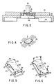
- FIGS. 3 to 6 a state where the IC 5 is pressed against the contactor 4 of the socket 2 and the configuration of the socket 2 will be explained.
- the base 2a of the socket 2 is placed on the frame F4.
- contact pins 2b are set straight at the base 2a.
- the tips of the contact pins 2b are inserted into the through holes 2a made in a protective plate 2c.
- the protective plate 2c are held above the base 2a by the four supports or protective pins 2e inserted into through holes made in the four corners of the plate 2c and the coil springs 2f provided around the protective pins 2e in such a manner that the plate 2c can move up and down.
- the coil springs 2f are normally set so that they may have such tension as raises the protective plate 2c to the extent that the contact pins 2b will not project from the surface of the protective plate 2c.
- FIG. 3 shows a state where the IC 5 stuck by suction to the tip of the pusher 8 has just come into contact with the protective plate 2c.
- the socket 2 put on the frame F4 is fixed and protected by covers 23 and 24.
- the IC 5 has a square shape of thin flat-plate and a plural number of lead pins 5b are stuck out from each side of a plate.
- the IC 5 is stuck by suction to the pusher 8 on the test hand 1
- the IC may be placed on the socket directly from the IC loader so as to be pressed by the pusher.
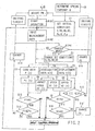
- the CPU 18 determines the pushing pressure, the allowable impact force, the working speed, and the thrusting displacement as follows.
- the thrusting displacement ⁇ of the pusher 8 is the distance from the position of the pusher 8 when the acceleration of the pusher 8 changes from zero to a specific negative value at the moment the IC 5 comes into contact with the protective plate 2c to the position to which the pusher 8 is lowered a specific distance predetermined by the IC 5, or to the position at which the pusher 8 is brought to a stop by the computer 14 when the pushing pressure load P has exceeded a prescribed value.
- the values of ⁇ 1 and ⁇ 2 are determined by the spring constants K1 and K2, respectively.
- the reaction force generated by the contact of the IC 5 with the socket protective plate 2c is equal to the pushing force P applied to the IC 5.
- the force P is detected by the load sensor 9 (load cell) provided above the pusher 8.
- the load sensor 9 load cell
- the impact force F can be evaluated as the product of m and acceleration as shown in the above equation.
- the pusher 8 of the test hand 1 presses repeatedly the IC 5 against the contactor 4 of the socket 2 or the protective plate 2c to measure the load P and displacement D, and then calculates the combined spring constant K of the IC 5 and socket 2 (step S0).
- the pushing pressure is set under the prescribed value given to the IC 5 and socket 2. Pressing the IC 5 more than once and averaging the results will minimize errors in the measured data of load P and displacement D, and then the more precise data may be obtained.
- the initial conditions including the operating velocity V of the test hand 1, the braking position HB and the position to be stopped HS of the test hand 1, the decreased velocity V0 after braking, the allowable thrusting displacement ⁇ a, and the allowable pushing pressure Pa, are inputted together with the combined spring constant K obtained at step S0 into the memory M.
- the pulse motor 3 driven by the driving circuit 17 is adjusted at step S21.
- the operator turns on the start switch at step S22, which starts the control operation. Then, the pulse motor 3 rotates at high speed and the pusher 8 of the test hand 1 moves downward rapidly from the initial position.
- the CPU 18 checks the number of revolutions of the pulse motor 3 by counting the number of pulses sent from the driving circuit 17. When the number of pulses has amounted to the number corresponding to the braking position of the test hand 1, the CPU 18 sends the driving circuit 17 an instruction to brake the pulse motor 3.
- the CPU 18 takes in the input data from the sensors 9 to 11 at step S23.
- load data P(t), acceleration data A(t), and displacement data D(t) at time t are stored in the memory M at steps S3, S4, and S5, respectively.
- the decreased velocity V1(t) of the pusher 8 is determined at step S7.
- the alternative decreased velocity V2(t) of the pusher 8 is determined at step S8.
- step S11 When the measured velocity is larger than the initial set value V0, the change of the braking position HB is set at step S11. Then, the control proceeds from step S24 to step S2, where the braking position HB is changed to a position closer to the socket S2.
- the contact pressure force P(t) between the IC 5 and socket 2 is measured directly by the load sensor 9 at step S3.
- This measured load is assigned to P1(t).
- the contact pressure force P(t) is calculated from the mass m of the pusher 8 and the acceleration A(t). The result of the calculation is P2(t).
- P1(t) is compared with P2(t) at step S12. Even when they are equal or differ slightly, the load, for example, P1(t) is compared with the allowable pushing pressure Pa in the memory M at step S13.
- the displacement data D(t) obtained at step S5, which is the thrusting displacement of the IC 5 to the socket 2 is compared with the allowed value ⁇ a in the memory M.
- D(t) exceeds ⁇ a
- the change of the stop position HS of the pusher 8 of the test hand 1 is set at step S16, and control returns from step S24 to step S2.
- the change of HS is made by changing the stroke of the pusher 8 of the test hand 1, or the total number of revolutions from the start to stop of the pulse motor 3.
- the operator can verify whether the operating speed of the pusher 8 is proper at step S10 or whether the operating states at steps S13 and S15 are acceptable. Therefore, when the original set values are proper, the operator use them as they are, whereas when they are improper, the operator corrects them. Furthermore, the capability of the test hand 1 to process the IC 5 can be maximized by increasing the operating speed V of the test hand 1 in the range that meets the requirements at steps S13 and S15. Since the IC 5 stuck by suction to the pusher 8 at the tip of the test hand 1 comes into contact with the socket 2 and is slowed down to V0 immediately before it is lowered further, the impact force can be limited considerably even when the operating speed V is somewhat large.
- test hand can be operated properly in a short time even with different types of ICs and sockets by incorporating the control method and instrumentation control system of the present invention into an IC handler.
- a method of controlling an IC handler according to the present invention and a control system using the method are used to cause a contact provided at the surface of an IC device to make good contact with the test probe of a semiconductor test unit in testing the IC device.
- the invention enables the operation to be performed quickly and accurately, which enables a large number of IC devices to be tested rapidly and accurately at the time of shipment.
Landscapes
- Engineering & Computer Science (AREA)
- Physics & Mathematics (AREA)
- General Physics & Mathematics (AREA)
- Computer Hardware Design (AREA)
- Microelectronics & Electronic Packaging (AREA)
- General Engineering & Computer Science (AREA)
- Testing Of Individual Semiconductor Devices (AREA)
- Investigating Strength Of Materials By Application Of Mechanical Stress (AREA)
- Manipulator (AREA)
- Selective Calling Equipment (AREA)
- Electrotherapy Devices (AREA)
- Drying Of Semiconductors (AREA)
Claims (11)
- Procédé pour commander un bras de test (1) pour appuyer un circuit intégré (5) chargé dans un support (2) d'un manipulateur de circuit intégré, comprenant les étapes consistant à :caractérisé par les étapes consistant à :déclencher l'appui du circuit intégré (5) par ledit bras de test (1) contre le support (2) plusieurs fois et détecter la charge, l'accélération ou la vitesse, et le déplacement de poussée du circuit intégré (5) par des capteurs correspondants (9 à 11) ;calculer la constante de rappel combinée pour le circuit intégré (5) et le support (2) d'après les éléments de données mesurés auparavant ; etdéterminer l'opération du bras de test (1) d'après la constante de rappel calculée de façon à ce que la force de choc exercée sur le circuit intégré (5) soit commandée pour être égale ou inférieure à une valeur permise.
- Procédé selon la revendication 1, comprenant en outre les étapes consistant à :comparer une force de compression se développant lorsque le pousseur (8) du bras de test (1) appuie sur le circuit intégré (5) placé sur le support (2) avec une force de pression permise prédéfinie ; etcommander l'opération du bras de test (1) à une force de pression égale ou inférieure à ladite force de pression permise sur la base du résultat de la comparaison.
- Procédé selon la revendication 2, caractérisé en ce qu'il comprend en outre l'étape consistant à calculer ladite force de pression permise prédéfinie à partir de la constante de rappel combinée pour le support (2) et le circuit intégré (5) auparavant.
- Procédé selon la revendication 2, caractérisé en ce qu'il comprend en outre l'étape consistant à commander ledit pousseur (8) de façon à ce que la vitesse de fonctionnement dudit pousseur (8) soit constante avant et après que ledit pousseur entre en contact avec le circuit intégré (5) sur ledit support (2).
- Procédé selon la revendication 3, caractérisé en ce que l'étape de calcul de la force de pression permise à partir de la constante de rappel combinée pour ledit support (2) et le circuit intégré (5) comprend l'étape consistant à prendre la moyenne des constantes de rappel combinées obtenues en déclenchant l'appui du circuit intégré (5) sur ledit support (2) sous l'action dudit pousseur (8) plusieurs fois.
- Système de commande des instruments pour un bras de test (1) comprenant :caractérisé parun capteur de charge (9) pour détecter la force de pression du bras de test (1) appliquée à un circuit intégré (5) chargé dans un support (2) ;un capteur de déplacement (11) pour mesurer le temps de déplacement de poussée à partir du moment où ledit bras de test (1) entre en contact avec le circuit intégré (5) jusqu'à la fin du contact ;
un capteur d'accélération (10) utilisé pour obtenir la vitesse de fonctionnement ou la détection de l'accélération dudit bras de test (1) ;
un moyen de commande (14), ledit moyen de commande (14) calculant la constante de rappel combinée pour le circuit intégré (5) et le support (2) sur la base des éléments de données provenant des capteurs individuels (9 à 11), obtenus en appuyant de manière répétée le circuit intégré sur le support, ledit moyen de commande (14) commandant également le pilotage du bras de test (1) sur la base des éléments de données individuels de façon à ce que la force de pression, la vitesse et le déplacement puissent atteindre des valeurs telles que l'action de la force de choc sur le circuit intégré (5) soit inférieure ou égale à une valeur permise tout en augmentant la vitesse de fonctionnement du bras de test (1) au maximum. - Système de commande des instruments selon la revendication 6, caractérisé en ce que ledit moyen de commande (14) possède une mémoire (M) pour stocker la vitesse en fonctionnement du bras de test (1), la position de freinage et la position d'arrêt du bras de test (1), et la vitesse en fonctionnement du bras de test (1) après le freinage, le déplacement de poussée permis et la force de pression permise en tant que conditions initiales au préalable.
- Système de commande des instruments selon la revendication 6, caractérisé en ce que ledit moyen de commande est adapté pour calculer ladite valeur permise à partir du déplacement de poussée du circuit intégré (5) et de ladite constante de rappel combinée.
- Système de commande des instruments selon la revendication 8, caractérisé en ce qu'il comprend en outre un moyen pour déplacer ledit bras de test (1) vers ladite position de freinage à vitesse élevée et, à partir de ladite position de freinage, déplacer ledit bras de test (1) à faible vitesse.
- Système de commande des instruments selon la revendication 6, caractérisé en ce qu'il comprend en outre un moniteur pour afficher le contenu de la commande exécutée par ledit moyen de commande (14).
- Système de commande des instruments selon la revendication 7, caractérisé en ce qu'il comprend en outre un moyen pour comparer lesdites conditions initiales définies avec les éléments de données mesurés provenant desdits capteurs individuels (9 à 11) et un moyen pour corriger lesdites conditions initiales lorsque le résultat de la comparaison a démontré que lesdits éléments de données mesurés diffèrent desdites conditions initiales.
Applications Claiming Priority (3)
| Application Number | Priority Date | Filing Date | Title |
|---|---|---|---|
| JP37854998 | 1998-12-31 | ||
| JP37854998A JP3407192B2 (ja) | 1998-12-31 | 1998-12-31 | テストハンドの制御方法及び計測制御システム |
| PCT/JP1999/007413 WO2000040983A1 (fr) | 1998-12-31 | 1999-12-28 | Procede de commande de manipulation d'ic, systeme de commande dans lequel ledit procede est utilise |
Publications (3)
| Publication Number | Publication Date |
|---|---|
| EP1069437A1 EP1069437A1 (fr) | 2001-01-17 |
| EP1069437A4 EP1069437A4 (fr) | 2003-04-23 |
| EP1069437B1 true EP1069437B1 (fr) | 2005-04-06 |
Family
ID=18509776
Family Applications (1)
| Application Number | Title | Priority Date | Filing Date |
|---|---|---|---|
| EP99962509A Expired - Lifetime EP1069437B1 (fr) | 1998-12-31 | 1999-12-28 | Procede de commande de manipulation d'ic, systeme de commande dans lequel ledit procede est utilise |
Country Status (11)
| Country | Link |
|---|---|
| US (1) | US6384734B1 (fr) |
| EP (1) | EP1069437B1 (fr) |
| JP (1) | JP3407192B2 (fr) |
| KR (1) | KR100394215B1 (fr) |
| CN (1) | CN1170166C (fr) |
| AT (1) | ATE292805T1 (fr) |
| CA (1) | CA2321868C (fr) |
| DE (1) | DE69924604T2 (fr) |
| SG (1) | SG98053A1 (fr) |
| TW (1) | TW484014B (fr) |
| WO (1) | WO2000040983A1 (fr) |
Cited By (1)
| Publication number | Priority date | Publication date | Assignee | Title |
|---|---|---|---|---|
| TWI717059B (zh) * | 2018-12-21 | 2021-01-21 | 日商賽納克股份有限公司 | 處理器 |
Families Citing this family (26)
| Publication number | Priority date | Publication date | Assignee | Title |
|---|---|---|---|---|
| US6690284B2 (en) * | 1998-12-31 | 2004-02-10 | Daito Corporation | Method of controlling IC handler and control system using the same |
| MY120838A (en) * | 2000-02-09 | 2005-11-30 | Synax Co Ltd | Method of controlling ic handler and control system using the same |
| JP2002365340A (ja) * | 2001-06-12 | 2002-12-18 | Mitsubishi Electric Corp | 基板検査装置および基板検査方法 |
| JP4548984B2 (ja) * | 2001-07-18 | 2010-09-22 | 株式会社リコー | Ic搬送装置 |
| WO2004059332A1 (fr) | 2002-12-25 | 2004-07-15 | Ricoh Company, Ltd. | Dispositif de transfert de circuit integre |
| JP2005116762A (ja) | 2003-10-07 | 2005-04-28 | Fujitsu Ltd | 半導体装置の保護方法及び半導体装置用カバー及び半導体装置ユニット及び半導体装置の梱包構造 |
| KR100707746B1 (ko) * | 2004-10-06 | 2007-04-17 | 가부시키가이샤 리코 | Ic 반송 장치 |
| DE102004058471A1 (de) * | 2004-11-24 | 2006-06-08 | Pilz Gmbh & Co. Kg | Sicherheitseinrichtung für eine automatisiert arbeitende Anlage mit zumindest einem automatisiert bewegbaren Anlagenteil |
| US7352198B2 (en) | 2006-01-18 | 2008-04-01 | Electroglas, Inc. | Methods and apparatuses for improved stabilization in a probing system |
| SG131792A1 (en) * | 2005-10-21 | 2007-05-28 | Daytona Control Co Ltd | Pusher of ic chip handler |
| US7214072B1 (en) * | 2005-10-31 | 2007-05-08 | Daytona Control Co., Ltd. | Pusher of IC chip handler |
| US7368929B2 (en) * | 2006-01-18 | 2008-05-06 | Electroglas, Inc. | Methods and apparatuses for improved positioning in a probing system |
| KR100813206B1 (ko) * | 2006-09-20 | 2008-03-13 | 미래산업 주식회사 | 전자부품 테스트용 핸들러 |
| US7825675B2 (en) * | 2006-11-01 | 2010-11-02 | Formfactor, Inc. | Method and apparatus for providing active compliance in a probe card assembly |
| KR100889819B1 (ko) * | 2007-06-05 | 2009-03-20 | 삼성전자주식회사 | 반도체 검사 장치 및 그 제어 방법 |
| KR100889379B1 (ko) * | 2007-07-03 | 2009-03-19 | 콘티넨탈 오토모티브 일렉트로닉스 주식회사 | 히트싱크와 하이브리드 집적회로 기판의 접합검사장치 |
| US8528885B2 (en) * | 2008-04-21 | 2013-09-10 | Formfactor, Inc. | Multi-stage spring system |
| JP5176867B2 (ja) * | 2008-10-24 | 2013-04-03 | セイコーエプソン株式会社 | 電子部品の押圧装置及びicハンドラ |
| US8120304B2 (en) | 2008-12-12 | 2012-02-21 | Formfactor, Inc. | Method for improving motion times of a stage |
| US8519728B2 (en) | 2008-12-12 | 2013-08-27 | Formfactor, Inc. | Compliance control methods and apparatuses |
| KR101375159B1 (ko) | 2012-09-28 | 2014-03-27 | 주식회사 아이디이오 | 로드셀을 포함하는 푸셔틀 및 반도체 테스트 시스템 |
| CN108054147B (zh) * | 2017-11-15 | 2020-05-15 | 中国科学院电工研究所 | 一种带有跳跃膜片的散热装置 |
| CN108172555B (zh) * | 2017-11-15 | 2020-05-15 | 中国科学院电工研究所 | 一种带有气体控水单元的散热装置 |
| KR102319388B1 (ko) * | 2020-07-16 | 2021-11-01 | 주식회사 아이에스시 | 검사용 커넥팅 장치 |
| JP7471190B2 (ja) * | 2020-09-30 | 2024-04-19 | 三菱電機株式会社 | 半導体素子特性検査装置 |
| WO2024232034A1 (fr) * | 2023-05-10 | 2024-11-14 | 株式会社Fuji | Dispositif de mesure |
Family Cites Families (18)
| Publication number | Priority date | Publication date | Assignee | Title |
|---|---|---|---|---|
| JPS61226287A (ja) * | 1985-03-07 | 1986-10-08 | エプシロン テクノロジー インコーポレーテツド | 加工品を取扱うたぬの装置および方法 |
| US4993266A (en) * | 1988-07-26 | 1991-02-19 | Kabushiki Kaisha Toyota Chuo Kenkyusho | Semiconductor pressure transducer |
| US5285946A (en) * | 1991-10-11 | 1994-02-15 | Sanyo Electric Co., Ltd. | Apparatus for mounting components |
| JPH05259242A (ja) * | 1992-03-16 | 1993-10-08 | Fujitsu Miyagi Electron:Kk | Icソケット |
| JPH0625724A (ja) | 1992-07-08 | 1994-02-01 | Nippon Steel Corp | 高炉ダストの処理方法 |
| JPH0664180U (ja) * | 1993-02-17 | 1994-09-09 | 株式会社アドバンテスト | Icハンドラにおける搬送装置 |
| JP2973785B2 (ja) * | 1993-08-19 | 1999-11-08 | 富士通株式会社 | Ic試験装置 |
| JP3184044B2 (ja) * | 1994-05-24 | 2001-07-09 | キヤノン株式会社 | 微動位置決め制御装置 |
| WO1996032696A1 (fr) * | 1995-04-13 | 1996-10-17 | Dai Nippon Printing Co., Ltd. | Carte et module de circuit integre |
| JPH08292230A (ja) * | 1995-04-20 | 1996-11-05 | Nec Yamaguchi Ltd | Icの電気特性測定装置およびその方法 |
| KR0163688B1 (ko) * | 1995-07-28 | 1999-03-20 | 전주범 | 내부회로 측정장치 |
| JPH0989983A (ja) | 1995-09-25 | 1997-04-04 | Ando Electric Co Ltd | Icの接触圧をデータで変えるic搬送装置 |
| KR100187727B1 (ko) * | 1996-02-29 | 1999-06-01 | 윤종용 | 처리기 접촉 불량을 확인할 수 있는 접촉 점검 장치 및 이를 내장한 집적회로 소자 검사 시스템 |
| US5814733A (en) * | 1996-09-12 | 1998-09-29 | Motorola, Inc. | Method of characterizing dynamics of a workpiece handling system |
| JP3494828B2 (ja) * | 1996-11-18 | 2004-02-09 | 株式会社アドバンテスト | 水平搬送テストハンドラ |
| JPH10160794A (ja) * | 1996-12-02 | 1998-06-19 | Mitsubishi Electric Corp | Ic着脱装置及びその着脱ヘッド |
| JPH10227834A (ja) | 1997-02-17 | 1998-08-25 | Ando Electric Co Ltd | Icのicソケットへの接触機構 |
| US6160410A (en) * | 1998-03-24 | 2000-12-12 | Cypress Semiconductor Corporation | Apparatus, method and kit for adjusting integrated circuit lead deflection upon a test socket conductor |
-
1998
- 1998-12-31 JP JP37854998A patent/JP3407192B2/ja not_active Expired - Lifetime
-
1999
- 1999-12-28 WO PCT/JP1999/007413 patent/WO2000040983A1/fr not_active Ceased
- 1999-12-28 EP EP99962509A patent/EP1069437B1/fr not_active Expired - Lifetime
- 1999-12-28 KR KR10-2000-7009282A patent/KR100394215B1/ko not_active Expired - Fee Related
- 1999-12-28 SG SG200202957A patent/SG98053A1/en unknown
- 1999-12-28 AT AT99962509T patent/ATE292805T1/de not_active IP Right Cessation
- 1999-12-28 DE DE69924604T patent/DE69924604T2/de not_active Expired - Lifetime
- 1999-12-28 CN CNB998034843A patent/CN1170166C/zh not_active Expired - Fee Related
- 1999-12-28 CA CA002321868A patent/CA2321868C/fr not_active Expired - Fee Related
- 1999-12-30 TW TW088123263A patent/TW484014B/zh not_active IP Right Cessation
-
2000
- 2000-08-28 US US09/651,572 patent/US6384734B1/en not_active Expired - Lifetime
Cited By (1)
| Publication number | Priority date | Publication date | Assignee | Title |
|---|---|---|---|---|
| TWI717059B (zh) * | 2018-12-21 | 2021-01-21 | 日商賽納克股份有限公司 | 處理器 |
Also Published As
| Publication number | Publication date |
|---|---|
| KR20010085197A (ko) | 2001-09-07 |
| HK1035402A1 (en) | 2001-11-23 |
| CA2321868A1 (fr) | 2000-07-13 |
| SG98053A1 (en) | 2003-08-20 |
| ATE292805T1 (de) | 2005-04-15 |
| CN1292092A (zh) | 2001-04-18 |
| EP1069437A4 (fr) | 2003-04-23 |
| EP1069437A1 (fr) | 2001-01-17 |
| JP3407192B2 (ja) | 2003-05-19 |
| US6384734B1 (en) | 2002-05-07 |
| CA2321868C (fr) | 2003-05-06 |
| TW484014B (en) | 2002-04-21 |
| DE69924604D1 (de) | 2005-05-12 |
| JP2000199779A (ja) | 2000-07-18 |
| KR100394215B1 (ko) | 2003-08-06 |
| WO2000040983A1 (fr) | 2000-07-13 |
| CN1170166C (zh) | 2004-10-06 |
| DE69924604T2 (de) | 2006-02-09 |
Similar Documents
| Publication | Publication Date | Title |
|---|---|---|
| EP1069437B1 (fr) | Procede de commande de manipulation d'ic, systeme de commande dans lequel ledit procede est utilise | |
| EP2363701B1 (fr) | Mécanisme de serrage amélioré pour appareil de test de cisaillement | |
| US6539809B1 (en) | Test apparatus for measuring stresses and strains | |
| US5422554A (en) | Vacuum nozzle capable of adjustable placing force | |
| JPH0613416A (ja) | ダイボンディング装置 | |
| US20080030212A1 (en) | Active probe contact array management | |
| TWI394955B (zh) | Contact load measuring device and inspection device | |
| EP1870714A1 (fr) | Carte sonde de microstructure et dispositif de verification de microstructure, procédé et programme informatique | |
| WO1996030772A1 (fr) | Dispositif de liaison pour materiel de test automatique | |
| US6690284B2 (en) | Method of controlling IC handler and control system using the same | |
| US7145642B2 (en) | Wafer support device and a wafer support method | |
| US7325298B2 (en) | Pressure apparatus and chip mounter | |
| US6336359B1 (en) | Impression forming mechanism and hardness testing apparatus | |
| US7284445B2 (en) | Strain waveform control apparatus, strain waveform regulating member, strain waveform control method by using strain waveform control apparatus, and strain waveform control program | |
| KR20070075757A (ko) | 반도체 소자 테스트 핸들러의 소자 접속장치 | |
| JPH10199940A (ja) | 部品搭載装置および部品搭載方法 | |
| JPH05322732A (ja) | 超微小材料試験機 | |
| JPH09189652A (ja) | 試験装置および方法 | |
| HK1035402B (en) | Method of controlling ic handler and control system using the same |
Legal Events
| Date | Code | Title | Description |
|---|---|---|---|
| PUAI | Public reference made under article 153(3) epc to a published international application that has entered the european phase |
Free format text: ORIGINAL CODE: 0009012 |
|
| 17P | Request for examination filed |
Effective date: 20000828 |
|
| AK | Designated contracting states |
Kind code of ref document: A1 Designated state(s): AT BE CH CY DE DK ES FI FR GB GR IE IT LI LU MC NL PT SE |
|
| A4 | Supplementary search report drawn up and despatched |
Effective date: 20030312 |
|
| 17Q | First examination report despatched |
Effective date: 20030610 |
|
| RAP1 | Party data changed (applicant data changed or rights of an application transferred) |
Owner name: DAYTONA CONTROL PTE LTD |
|
| GRAP | Despatch of communication of intention to grant a patent |
Free format text: ORIGINAL CODE: EPIDOSNIGR1 |
|
| GRAS | Grant fee paid |
Free format text: ORIGINAL CODE: EPIDOSNIGR3 |
|
| GRAA | (expected) grant |
Free format text: ORIGINAL CODE: 0009210 |
|
| AK | Designated contracting states |
Kind code of ref document: B1 Designated state(s): AT BE CH CY DE DK ES FI FR GB GR IE IT LI LU MC NL PT SE |
|
| PG25 | Lapsed in a contracting state [announced via postgrant information from national office to epo] |
Ref country code: LI Free format text: LAPSE BECAUSE OF FAILURE TO SUBMIT A TRANSLATION OF THE DESCRIPTION OR TO PAY THE FEE WITHIN THE PRESCRIBED TIME-LIMIT Effective date: 20050406 Ref country code: FI Free format text: LAPSE BECAUSE OF FAILURE TO SUBMIT A TRANSLATION OF THE DESCRIPTION OR TO PAY THE FEE WITHIN THE PRESCRIBED TIME-LIMIT Effective date: 20050406 Ref country code: CH Free format text: LAPSE BECAUSE OF FAILURE TO SUBMIT A TRANSLATION OF THE DESCRIPTION OR TO PAY THE FEE WITHIN THE PRESCRIBED TIME-LIMIT Effective date: 20050406 Ref country code: BE Free format text: LAPSE BECAUSE OF FAILURE TO SUBMIT A TRANSLATION OF THE DESCRIPTION OR TO PAY THE FEE WITHIN THE PRESCRIBED TIME-LIMIT Effective date: 20050406 Ref country code: AT Free format text: LAPSE BECAUSE OF FAILURE TO SUBMIT A TRANSLATION OF THE DESCRIPTION OR TO PAY THE FEE WITHIN THE PRESCRIBED TIME-LIMIT Effective date: 20050406 |
|
| REG | Reference to a national code |
Ref country code: GB Ref legal event code: FG4D |
|
| REG | Reference to a national code |
Ref country code: CH Ref legal event code: EP |
|
| REG | Reference to a national code |
Ref country code: IE Ref legal event code: FG4D |
|
| REF | Corresponds to: |
Ref document number: 69924604 Country of ref document: DE Date of ref document: 20050512 Kind code of ref document: P |
|
| PG25 | Lapsed in a contracting state [announced via postgrant information from national office to epo] |
Ref country code: SE Free format text: LAPSE BECAUSE OF FAILURE TO SUBMIT A TRANSLATION OF THE DESCRIPTION OR TO PAY THE FEE WITHIN THE PRESCRIBED TIME-LIMIT Effective date: 20050706 Ref country code: GR Free format text: LAPSE BECAUSE OF FAILURE TO SUBMIT A TRANSLATION OF THE DESCRIPTION OR TO PAY THE FEE WITHIN THE PRESCRIBED TIME-LIMIT Effective date: 20050706 Ref country code: DK Free format text: LAPSE BECAUSE OF FAILURE TO SUBMIT A TRANSLATION OF THE DESCRIPTION OR TO PAY THE FEE WITHIN THE PRESCRIBED TIME-LIMIT Effective date: 20050706 |
|
| PG25 | Lapsed in a contracting state [announced via postgrant information from national office to epo] |
Ref country code: ES Free format text: LAPSE BECAUSE OF FAILURE TO SUBMIT A TRANSLATION OF THE DESCRIPTION OR TO PAY THE FEE WITHIN THE PRESCRIBED TIME-LIMIT Effective date: 20050717 |
|
| PG25 | Lapsed in a contracting state [announced via postgrant information from national office to epo] |
Ref country code: PT Free format text: LAPSE BECAUSE OF FAILURE TO SUBMIT A TRANSLATION OF THE DESCRIPTION OR TO PAY THE FEE WITHIN THE PRESCRIBED TIME-LIMIT Effective date: 20050908 |
|
| REG | Reference to a national code |
Ref country code: CH Ref legal event code: PL |
|
| PGFP | Annual fee paid to national office [announced via postgrant information from national office to epo] |
Ref country code: NL Payment date: 20051130 Year of fee payment: 7 Ref country code: FR Payment date: 20051130 Year of fee payment: 7 |
|
| PG25 | Lapsed in a contracting state [announced via postgrant information from national office to epo] |
Ref country code: IT Free format text: LAPSE BECAUSE OF NON-PAYMENT OF DUE FEES Effective date: 20051228 Ref country code: CY Free format text: LAPSE BECAUSE OF FAILURE TO SUBMIT A TRANSLATION OF THE DESCRIPTION OR TO PAY THE FEE WITHIN THE PRESCRIBED TIME-LIMIT Effective date: 20051228 |
|
| PGFP | Annual fee paid to national office [announced via postgrant information from national office to epo] |
Ref country code: GB Payment date: 20051228 Year of fee payment: 7 |
|
| PG25 | Lapsed in a contracting state [announced via postgrant information from national office to epo] |
Ref country code: IE Free format text: LAPSE BECAUSE OF NON-PAYMENT OF DUE FEES Effective date: 20051229 |
|
| PG25 | Lapsed in a contracting state [announced via postgrant information from national office to epo] |
Ref country code: MC Free format text: LAPSE BECAUSE OF NON-PAYMENT OF DUE FEES Effective date: 20051231 Ref country code: LU Free format text: LAPSE BECAUSE OF NON-PAYMENT OF DUE FEES Effective date: 20051231 |
|
| PLBE | No opposition filed within time limit |
Free format text: ORIGINAL CODE: 0009261 |
|
| STAA | Information on the status of an ep patent application or granted ep patent |
Free format text: STATUS: NO OPPOSITION FILED WITHIN TIME LIMIT |
|
| ET | Fr: translation filed | ||
| 26N | No opposition filed |
Effective date: 20060110 |
|
| REG | Reference to a national code |
Ref country code: IE Ref legal event code: MM4A |
|
| PG25 | Lapsed in a contracting state [announced via postgrant information from national office to epo] |
Ref country code: NL Free format text: LAPSE BECAUSE OF NON-PAYMENT OF DUE FEES Effective date: 20070701 |
|
| GBPC | Gb: european patent ceased through non-payment of renewal fee |
Effective date: 20061228 |
|
| NLV4 | Nl: lapsed or anulled due to non-payment of the annual fee |
Effective date: 20070701 |
|
| REG | Reference to a national code |
Ref country code: FR Ref legal event code: ST Effective date: 20070831 |
|
| PG25 | Lapsed in a contracting state [announced via postgrant information from national office to epo] |
Ref country code: GB Free format text: LAPSE BECAUSE OF NON-PAYMENT OF DUE FEES Effective date: 20061228 |
|
| PG25 | Lapsed in a contracting state [announced via postgrant information from national office to epo] |
Ref country code: FR Free format text: LAPSE BECAUSE OF NON-PAYMENT OF DUE FEES Effective date: 20070102 |
|
| PGRI | Patent reinstated in contracting state [announced from national office to epo] |
Ref country code: IT Effective date: 20090401 |
|
| PGRI | Patent reinstated in contracting state [announced from national office to epo] |
Ref country code: IT Effective date: 20090401 |
|
| PGRI | Patent reinstated in contracting state [announced from national office to epo] |
Ref country code: IT Effective date: 20110616 |
|
| REG | Reference to a national code |
Ref country code: DE Ref legal event code: R082 Ref document number: 69924604 Country of ref document: DE Representative=s name: V. BEZOLD & PARTNER, DE Effective date: 20111208 Ref country code: DE Ref legal event code: R082 Ref document number: 69924604 Country of ref document: DE Representative=s name: V. BEZOLD & PARTNER PATENTANWAELTE - PARTG MBB, DE Effective date: 20111208 Ref country code: DE Ref legal event code: R081 Ref document number: 69924604 Country of ref document: DE Owner name: SYNAX CO., LTD., JP Free format text: FORMER OWNER: DAYTONA CONTROL PTE LTD., SINGAPORE, SG Effective date: 20111208 Ref country code: DE Ref legal event code: R081 Ref document number: 69924604 Country of ref document: DE Owner name: SYNAX CO., LTD., NISHIHARA MATSUOMOTO-SHI, JP Free format text: FORMER OWNER: DAYTONA CONTROL PTE LTD., SINGAPORE, SG Effective date: 20111208 |
|
| PGFP | Annual fee paid to national office [announced via postgrant information from national office to epo] |
Ref country code: IT Payment date: 20131111 Year of fee payment: 15 |
|
| PGFP | Annual fee paid to national office [announced via postgrant information from national office to epo] |
Ref country code: DE Payment date: 20140207 Year of fee payment: 15 |
|
| REG | Reference to a national code |
Ref country code: DE Ref legal event code: R119 Ref document number: 69924604 Country of ref document: DE |
|
| PG25 | Lapsed in a contracting state [announced via postgrant information from national office to epo] |
Ref country code: DE Free format text: LAPSE BECAUSE OF NON-PAYMENT OF DUE FEES Effective date: 20150701 |
|
| PG25 | Lapsed in a contracting state [announced via postgrant information from national office to epo] |
Ref country code: IT Free format text: LAPSE BECAUSE OF NON-PAYMENT OF DUE FEES Effective date: 20141228 |