EP1068630B1 - Microscope electronique a balayage - Google Patents
Microscope electronique a balayage Download PDFInfo
- Publication number
- EP1068630B1 EP1068630B1 EP99914503A EP99914503A EP1068630B1 EP 1068630 B1 EP1068630 B1 EP 1068630B1 EP 99914503 A EP99914503 A EP 99914503A EP 99914503 A EP99914503 A EP 99914503A EP 1068630 B1 EP1068630 B1 EP 1068630B1
- Authority
- EP
- European Patent Office
- Prior art keywords
- detector
- sample
- pressure stage
- scanning electron
- secondary electrons
- Prior art date
- Legal status (The legal status is an assumption and is not a legal conclusion. Google has not performed a legal analysis and makes no representation as to the accuracy of the status listed.)
- Expired - Lifetime
Links
Images


Classifications
-
- H—ELECTRICITY
- H01—ELECTRIC ELEMENTS
- H01J—ELECTRIC DISCHARGE TUBES OR DISCHARGE LAMPS
- H01J37/00—Discharge tubes with provision for introducing objects or material to be exposed to the discharge, e.g. for the purpose of examination or processing thereof
- H01J37/26—Electron or ion microscopes; Electron or ion diffraction tubes
- H01J37/28—Electron or ion microscopes; Electron or ion diffraction tubes with scanning beams
-
- H—ELECTRICITY
- H01—ELECTRIC ELEMENTS
- H01J—ELECTRIC DISCHARGE TUBES OR DISCHARGE LAMPS
- H01J37/00—Discharge tubes with provision for introducing objects or material to be exposed to the discharge, e.g. for the purpose of examination or processing thereof
- H01J37/02—Details
- H01J37/244—Detectors; Associated components or circuits therefor
-
- H—ELECTRICITY
- H01—ELECTRIC ELEMENTS
- H01J—ELECTRIC DISCHARGE TUBES OR DISCHARGE LAMPS
- H01J2237/00—Discharge tubes exposing object to beam, e.g. for analysis treatment, etching, imaging
- H01J2237/26—Electron or ion microscopes
- H01J2237/2602—Details
- H01J2237/2605—Details operating at elevated pressures, e.g. atmosphere
- H01J2237/2608—Details operating at elevated pressures, e.g. atmosphere with environmental specimen chamber
Definitions
- the invention relates to a scanning electron microscope (SEM), in particular a below something high-pressure scanning electron microscope or the conversion of one under vacuum operated scanning electron microscope for operation with gas in the sample chamber, and relates In particular, an improved detection efficiency of such a microscope (i.e. Improvement of the signal-to-noise ratio of the pictures taken with it), in particular when operating with low primary energy.
- SEM scanning electron microscope
- the backscatter electrons emitted by the sample can be detected.
- a better spatial resolution is obtained when using the sample emitted secondary electrons, which can be detected by means of a collector electrode (WO 88/09564 A1).
- a collector electrode usually the underside of the pressure stage aperture as a collector electrode formed or arranged a separate collector electrode below the pressure stage aperture.
- Detector systems with collector electrodes have the following due to the noise electronic amplification a poor detection sensitivity and therefore require a Pre-amplification of the secondary electron signal before reaching the collector electrode, this Preamplification takes place by means of an electric field between the sample and the collector electrode, by which the secondary electrons emitted by the sample are accelerated so that they can ionize gas molecules. After the collision with the gas molecules they are in the gas generated secondary electrons and the already existing secondary electrons again the electric field accelerates and generates further secondary electrons in the gas. In this way becomes a secondary electron cascade by the secondary electrons emitted by the sample which finally reaches the collector electrode. Also when using a light guide with a downstream photomultiplier as a gas scintillation detector becomes a secondary electron cascade used as a pre-amplification.
- the signal-to-noise ratio is in both cases the images taken at slightly elevated pressure, at the same beam current strength substantially worse than the pictures taken without increased pressure with conventional secondary electron detectors be recorded.
- sensitive samples for example Semiconductor devices, plastics, biological and medical samples
- the use of a low is still Primary energy advantageous to supply the sample with less energy and the damage of the To limit the sample to a thin surface layer by the electron beam.
- the previously known Pressure SEMs require a secondary electron cascade in their collector electrode Gas and therefore are for operation with low primary energy (for example, 1 keV), in particular in the observation of wet samples, unsuitable.
- low primary energy for example, 1 keV
- the invention is based on the object, an improved, working under somewhat elevated pressure SEM (hereinafter referred to as pressure-scanning electron microscope or pressure SEM) which does not have the mentioned disadvantages of conventional pressure SEMs, and in particular the detection efficiency of pressure SEMs in which the detection of the secondary electrons emitted by the sample takes place through the pressure stage diaphragm, through which the microscope column is closed to the sample chamber (or the signal-to-noise ratio the images taken), especially when operating with low primary energy to improve.
- pressure SEM pressure-scanning electron microscope
- the invention is generally based on the idea of a scanning electron microscope with the Further develop features according to the preamble of claim 1 so that as a detector highly sensitive, compared to the sample positively biased detector is used.
- the object is more particularly according to a first aspect further in particular solved in that above the pressure level diaphragm one or more electrode elements (solid electrodes or thin electrode layers) are arranged opposite to the Pressure gradient are on positive potential, using as a detector for in the sample and in the Gas generated secondary electrons no collector electrode, but one or more detectors be used with higher detection sensitivity.
- one or more electrode elements solid electrodes or thin electrode layers
- the advantage of the invention is in particular that - regardless of the presence a secondary electron cascade - a high detection efficiency for that of the sample emitted secondary electrons and a low noise of the detector system can be achieved.
- the pressure SEMs according to the invention the length of the path, the primary electrons through the gas must be made very small ( ⁇ 300 microns) by a short distance is used between the sample and the pressure level stop and above the pressure level stop is pumped out.
- the previously known pressure SEMs are for such short distances ( ⁇ 300 microns) of the primary electrons by the gas, however, in principle unsuitable because neither a sufficient secondary electron cascade either below or above the pressure stage diaphragm can train.
- the scanning electron microscopy at low Primary energy for example, 1 keV and less
- gas in the sample chamber for example Steam at a pressure of 10 hPa
- the high detection efficiency and the low noise of the detector system is only a small beam current required. This allows moist samples at higher magnifications than before without drying out observed sample spot are observed.
- the boot fight an important improvement when operating with low primary energy and good detection efficiency the previous possibilities.
- the pressure SEMs according to the invention produce high primary energy (> 15 keV) Scanning electron microscopy with secondary electrons at unusually high pressure (> 100 hPa) possible.
- high primary energy > 15 keV
- secondary electrons at unusually high pressure (> 100 hPa) possible.
- a pressure stage with a very small bore diameter for example, 20 microns
- very small distances ⁇ 50 microns
- first and second aspects of the invention can be used individually or be implemented together to solve the above-mentioned problem. In both cases will the acceleration of secondary electrons from a near-sample area with increased pressure towards the detector into a sample area with reduced pressure (vacuum).
- a preferred embodiment of the invention is therefore that the entire Detector surface or parts of the detector surface are at a potential opposite the potential of the sample is more than 500 V, preferably 1000 V positive.
- the use of such Detectors in the sample chamber of a conventional pressure SEM would turn over to lead.
- a preferred embodiment of the invention is that the pressure-SEM a has combined electrostatic and magnetic objective lens.
- the pressure-SEM a has combined electrostatic and magnetic objective lens.
- DE 3703029 A1 is this particular of Advantage, if the so-configured pressure-SEM also both usual primary energies above 3 keV should be used.
- a combined electrostatic and magnetic objective lens particularly advantageous if the secondary electrons focused by an electric field on the opening of a pressure level stop should be.
- the improved detection efficiency comes from an increase in the proportion of in the Sample and generated in the gas secondary electrons passing through the Druckissuenblenden get to the detector.
- this proportion increased because the secondary electrons move on spiral paths around the magnetic field lines, which pass through the openings of the Druckissuenblenden.
- the secondary electrons are impacted by new spiral paths around neighboring field lines but with sufficient magnetic field strength mostly also through the openings go through the pressure stage apertures.
- the realization of the invention is not limited to pressure-SEMs, but can by Retrofitting is also possible with REMs, which are normally operated with evacuated sample chamber become.
- REMs which are normally operated with evacuated sample chamber become.
- the easy conversion between the two applications provides an advantage of Invention.
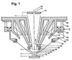
- the primary electron beam passes along the optical axis 79 from above through the opening 77 of the detector 74th
- the Abrastem the sample 11 required deflection of the primary electron beam is generated by means of the deflection coils 59 .
- the focusing of the primary electron beam is effected by means of the electrostatic lens formed by the electrodes 44, 50 and 55 and the magnetic field generated by the magnetic lens 62 and / or the magnetic einpollinse 64 . Another contribution to the focusing of the primary electron beam is provided by the electric field between the electrode 44 and the electrode 18. It is also possible to omit the magnetic lens 62 with the pole gap opened to the optical axis or the magnetic one-pole lens 64 .
- the electrode 55 is opposite the electrodes 44 and 50 at a strongly positive potential.
- the potential difference is preferably 1 to 15 kV and may be 7 keV, for example.
- the electrodes 50 and 44 are centered over the insulation 56 on the pole piece 58 .
- the electrode 44 is opposite the electrode 18 to positive potential with a preferred potential difference of 50 to 2000 V.
- the electrode 18, which is secured via the insulation 60 is opposite to the sample 11 at a positive or at the same potential. The magnitude of the applied voltages will be discussed below in connection with FIG. 2.
- the two electrodes 18 and 44 form an electrostatic lens, it is advantageous for the resolution that the truncated conical electrode 18 can be centered with great accuracy with respect to the optical axis 79 during operation.
- a suitable possibility for this is, for example, the use of micrometer screws and / or controlled piezo-actuator systems whose force effects F X and F Y (in the x and y directions) elastically deform the round rods 68 distributed over the circumference in the illustrated embodiment.
- the electrode 44 need not be centered as accurately as the electrode 18 , since the equipotential surfaces of the electric field in the region of the opening 41 of the electrode 44 are almost flat.
- the electrodes 18 and 44 are simultaneously designed as pressure stage diaphragms. Through the opening of the pressure stage aperture 18 gas flows from the sample chamber up into the microscope column, which is pumped through the corrugated tube 63 and through the opening of the electrode 55 , as indicated by the arrows. The sealing of the centerable pressure stage diaphragm 18 with respect to the outer pole piece takes place through the Simmerring 65.
- those components 18, 44, 50, 56, 60, 63, 65, 68, 69 ) which, when operating with vacuum in the sample chamber, represent an unnecessary limitation to the field of view and the working distance, can be easily expanded to operate the pressure SEM in vacuum operation without it with another electrode 50 .
- the component 69 can be unscrewed from the overlying part and the insulation 56 is easily removable mounted on the pole piece 58 .
- the pressure level aperture 18 is easily replaceable, so that depending on the application pressure level apertures can be used with different sized openings.
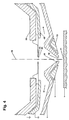
- FIG. 1 An enlarged detail of FIG. 1 with the pressure stage apertures 18 and 44 and the sample 11 is shown schematically in FIG.
- the electrode 44 is opposite to the electrode 18 to a positive potential whose size is chosen so that directly above and directly below the opening 41 about the same electric field strength prevails. This ensures that the curvature of the equipotential surfaces in the region of the opening 41 is as weak as possible.
- the upper pressure step aperture 44 is very thin to cause the least possible curvature of the equipotential surfaces in the vicinity of the optical axis. Their preferred thickness near the optical axis is less than 300 ⁇ m and greater than 0.4 ⁇ m (eg 20 ⁇ m).
- It can either consist of metal (for example as a thin-film diaphragm which can also be heated with the primary electron beam if required) or can be produced by etching, in particular, of semiconductor material (for example silicon). In the latter case, either a thin layer of the semiconductor may be left standing during etching or only a metal layer previously deposited on the semiconductor may be left over.
- metal for example as a thin-film diaphragm which can also be heated with the primary electron beam if required
- semiconductor material for example silicon
- the preferred size of the apertures 16 and 41 of the pressure stage orifices in Figure 2 is dependent upon the desired maximum allowable pressure in the sample chamber, the desired minimum usable primary energy, the voltage and spacing between the electrodes 18 and 44, and the quality of the vacuum that requires the cathode (for example, a Schottky emitter).
- the diameter of the opening 16 of the pressure stage diaphragm 18 may be, for example, 20 ⁇ m to 500 ⁇ m. However, without the ability to withstand low primary energies, or limited to low pressures in the sample chamber, the size of the opening 16 may be 1000 ⁇ m, for example.
- the preferred diameter of the opening 41 may be, for example, 100 microns to 2000 microns. It is preferably at least as large as the diameter of the opening 16 .
- the underside 14 and the lower region of the outer side 15 of the pressure stage diaphragm are n-doped and vapor-deposited with a thin metal layer, so that a Schottky contact is formed.
- the primary electron beam enters the sample chamber from above through the opening 16 in FIG. 2, traverses the gas in the sample chamber and strikes the sample 11 , where it generates secondary electrons and backscattered electrons.
- the secondary electrons have a large cross section for elastic scattering. Their direction of movement is therefore, as in a diffusion process, often deflected and there is a risk that they are absorbed by the sample.
- the secondary electrons are therefore directed by means of an electric field to the opening 16 , which consists either only of the field penetration through the opening 16 or by the additional application of a voltage between the sample 11 and the pressure level aperture 18 is generated.
- Applying a voltage between the sample 11 and the pressure stage orifice 18 has several effects: it creates a stronger electric field, thereby enhancing the transport of the secondary electrons up to the pressure stage orifice 18. At the same time, it reduces the bulging of the equipotential surfaces downwardly within and just below the orifice 16 , so that the secondary electrons are less strongly directed to the optical axis 79 in this area. On the other hand, however, together with the frusto-conical electrode 18, it causes the secondary electrons to be directed further below the opening 16 toward the optical axis 79 .
- a secondary electron cascade For larger distances (for example, 1000 microns) and larger voltages (for example, 200 V) between the sample 11 and the pressure level aperture 18 is obtained a secondary electron cascade as additional preamplification.
- a sufficiently large pressure stage aperture 16 > 200 microns, for example, 250 microns get enough secondary electrons in the opening 16, so as to obtain a good detection efficiency hereby with larger distances.
- a pressure stage diaphragm 18 is preferred, as shown in Fig. 5, which has no cylinder jacket-shaped bore wall 17 , but instead has only a sharp inner edge as a boundary between the bottom 14 and the top 22 of the pressure stage aperture.
- the magnetic field generated by the one-pole lens 64 depicted in FIG. 1 is also very helpful in transporting the secondary electrons to the aperture 16 and through the aperture 16 therethrough. Due to the magnetic field, the motion component of the secondary electrons, which is perpendicular to the optical axis 79 , is deflected by means of the Lorentz force onto a circular path. This ensures that a secondary electron emitted by the sample on its way up can increase its distance from the optical axis 79 between two collisions by a maximum of its double Larmorradius.
- the low-energy secondary electrons whose cross-section is particularly high for elastic scattering, have favorably also a particularly small Larmorradius.
- the secondary electrons with an energy of more than 10 eV is added to favor that smaller scattering angles are much more likely than large scattering angles. This results in that the distance between the circle centers of the movement before the impact and after the impact is substantially less than the sum of the two Larmorradien. Since the secondary electrons can move away from the optical axis 79 less far, when using a one-pole lens, more secondary electrons pass through the opening 16 of the pressure stage diaphragm than without a monopole lens.
- the magnetic field of the one-pole lens 64 also plays an important role, if present.
- the pressure stage apertures are arranged so that the magnetic field lines passing through the aperture of the lower pressure stage aperture 18 also pass through the aperture 41 of the upper pressure stage aperture. (This is the case, for example, if the opening of the upper pressure stage aperture 44 is not substantially smaller than the opening of the lower pressure stage aperture 18 and the upper pressure stage aperture 44 is mounted below the pole piece 58 , as shown in FIGS. 1, 6, 7, 8, 9 and 10).
- the pressure up to the opening 41 of the upper pressure stage diaphragm 44 decreases by several orders of magnitude relative to the pressure of the sample chamber.
- the pressure decrease is dependent on the size of the opening 16 of the lower pressure level aperture. This decrease in pressure at the top causes an increase in the mean free path of the secondary electrons.
- the secondary electrons are focused in the embodiments of FIGS. 2 to 4 by the electric field between the two pressure stage apertures on the upper Drucklienblendenö réelle 41 , above which there is a good vacuum in which the Secondary electrons are detected.
- the focusing of the secondary electrons on the opening 41 is achieved by suitably selecting the position of the electrode 44 : when the electrode 50 is made slightly longer and thereby the Electrode 44 (with correspondingly smaller outer diameter) is arranged slightly further down, one obtains a lower electric field strength in the opening 41. Accordingly, the potential difference between the electrodes 18 and 44 is reduced so much that directly below the opening 41 again the same field strength prevails as in the opening 41 . This results in a weaker focusing of the secondary electrons, while at the same time the distance is shortened on which the secondary electrons are focused. (Due to the smaller potential difference between the electrodes 18 and 50 , this distance can be further shortened by reducing the distance between the two electrodes.)
- a preferred embodiment is that the focusing of the secondary electrons on the Opening 41 can be adjusted. (There is no need for a large change in focusing.) Focusing of the secondary electrons on the aperture 41 is achieved, for example, when the voltage between the electrodes 18 and 44 and, in proportion thereto, the voltage between the electrodes 44 and 55 can be varied. Another possibility is. that one of the pressure stage apertures 18 or 44 is adjustable in height (ie adjustable in position along the optical axis).
- Another way to change the focus results when using a non-acting as a pressure level stop, additional electrode with a larger opening diameter, which is mounted between the electrodes 18 and 44 and preferably secured and centered on an insulation on one of these two electrodes.
- the potentials of the electrode 18 and the additional electrode can then be varied so that the equipotential surfaces in the opening 41 remain flat while the focusing of the secondary electrons is changed.
- the adjustable or variable focusing of the electrons mentioned here is important in particular for large pressure stage apertures 16 .
- the further path of the secondary electrons above the electrode 44 will be explained below with reference to FIG. 1.
- the secondary electrons are further accelerated by the electric field between the electrodes 44 and 55 and fly to the detector 74 with high kinetic energy .
- the large decrease in gas pressure within and above the pressure stage apertures 18 and 44 achieves that, despite the increased pressure in the sample chamber
- a sufficiently good vacuum for the use of detectors with high detection sensitivity is present.
- scintillator-light guide combinations, channelplates and semiconductor detectors with a metal-semiconductor junction or with a pn junction are well suited as the detector 74 .
- Scintillator photomultiplier combinations based on plastic scintillators, YAG scintillators, YAP scintillators and the like can also be used.
- a channelplate it is advisable to provide an additional liner electrode for the opening of the detector, as used in DE 3703029 A1.
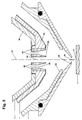
- FIG. 3 shows, for the same section as in FIG. 2, another variant of a pressure SEM according to the invention for illustrating the above-mentioned second aspect.
- the upper pressure step diaphragm in FIG. 3 is constructed in layers: its underside 39 and upper side 43 are made of conductive materials, while in their interior there is at least one layer of insulating material. The contacting of the conductive layers 39 and 43 is outside the range shown.
- the potentials of the electrodes 18, 39 and 43 are selected so that the same electric field strength prevails in the openings of the electrodes 39 and 43 and in the region 41 between the openings of the two electrodes. Since the preferred thickness of the electrodes 39 and 43 in the vicinity of the optical axis 79 is very small ( ⁇ 100 ⁇ m), the equipotential surfaces in the region of the openings of the electrodes 39 and 43 and in the region 41 therebetween are almost flat. The preferred distance between the electrodes 39 and 43 is 10 to 1000 ⁇ m.
- a suitable way of producing such a layered pressure stage shutter with very thin electrodes 39 and 43 is, for example, that the electrodes 39 and 43 represent metal coatings of an insulator, between which the insulator has been etched away in a region around the optical axis.
- the opening of the electrode 39 may also be equal to or larger than the opening of the electrode 43 and more than two conductive layers may be used.
- the lower pressure level aperture 18 can be constructed in layers.
- the conductive layers may in particular be flat, conical or frustoconical.
- the use of a layered lower pressure stage shutter 18 has particular advantages in that the transport of the secondary electrons to the detector is improved, the field of view can be increased and that the error coefficient of the electrostatic lens adjacent to the pressure stage shutter can be reduced.
- FIG. 4 shows a section with the pressure step diaphragms for another variant of a pressure SEM according to the invention.
- the difference from the variant of FIG. 2 consists in the additional support 40 for the pressure level aperture 44 and in that the electrode 50 is executed in Fig. 4 without the intermediate insulation 56 as a direct continuation of the pole piece 58 , so that they are particularly good Centering with respect to the optical axis and is grounded.
- the electrode 50 is not removable, while the parts 13, 18, 40, 42 and 44 (and 60, 63, 65, 68 and 69 of Fig. 1) for the operation of the pressure SEM with vacuum in the sample chamber can be removed.
- the remainder of the REM for the vacuum operation, apart from the additional one-pole lens, largely corresponds to the conventional designs of REMs, as offered, for example, by the companies "ICT" or "LEO".
- the holder 40 which is designed as a spring element, holds the pressure stage diaphragm 44 , which is centered on the bore of the electrode 50 , in its position. It would also be possible to use as a holder a spring element which is supported by an insulation on the underlying component 18 . Further, one could also center the pressure stage aperture 18 on the correspondingly redesigned outer edge of the electrode 50 . It is also possible to omit the upper pressure stage aperture 44, its holder 40 and the additional pumping through the corrugated hose 63 (see Fig. 1).
- FIG. 5 shows an exemplary embodiment in which the secondary electrons do not have to be focused on a specific location even without the magnetic field of the one-pole lens, and accordingly the parameters relevant for the secondary electron focusing can also be freely selected.
- Another advantage of the embodiment shown in Fig. 5 is that even without the magnetic field of the Einpollinse 64 contributes a very large proportion of the secondary electrons to the signal of the detector.
- the path of the primary electron beam through the openings 41 and 16 to the sample 11, the voltage between the sample 11 and the pressure stage aperture 18, the path of the secondary electrons from the sample 11 to the opening 16 and through the opening 16 , the size of the opening 16, the Increase in the electric field strength above the opening 16 and the pressure decrease above the opening 16 are the same as in Fig. 2.
- the thick-walled component 42 is used instead of the thin-walled pressure stage aperture 44 in Fig. 2, however, the thick-walled component 42 is used. Its preferred thickness (length of the passage 41 ) is 0.4 mm to 6 mm. It is constructed in layers of insulating and conductive layers which are perpendicular to the optical axis 79 and are indicated in FIG. 5 by the horizontal hatching of the component 42 .
- the conductive layers have a preferred thickness of less than 200 microns, while the insulating layers can be thicker.
- the component 42 is fitted in the insulating holder 40 , which centered the component 42 on the bore of the electrode 50 .
- the upper surface of the component 42 is covered by the conductive layer 43 , which forms an electrode which is at the same potential as the electrode 50 .
- the undersides of the component 42 and the holder 40 are covered by the conductive layer 39 . It forms an electrode which is opposite to the electrode 43 at a negative potential.
- the component 42 has a central passage 41 around the optical axis 79 around and additionally several passages 36 distributed over the circumference.
- the surface of the vias 36 and 41 is covered with a poorly conductive layer, the electrical parameters of which correspond, for example, to those of a poorly conductive layer, as used in a channeltron or a channelplate.
- the poorly conductive layer in the passages 36 and 41 has a total resistance uniformly distributed along the optical axis. (In order to achieve a uniform distribution of the resistance along the optical axis, an additional poorly conductive layer may also be applied to the component 40 on the component 42 ). This results in a homogeneous electric field in the passages 36 and 41 between the electrodes 39 and 43 , with which the poorly conductive layer is contacted.
- the layered structure of the component 42 of alternating thin insulating and conductive layers results in a somewhat irregular distribution of the poorly conductive layer in the passage 41 a rotationally symmetric electric field, so that a good resolution is achieved.
- the magnitude of the voltage between the electrodes 50 and 55 has been discussed in connection with FIG.
- the voltage between the electrodes 39 and 43 is so large that the electric field strength within the passage 41 is the same as directly above the passage 41 .
- the voltage between the electrodes 25 and 39 is so large that the electric field strength directly below the passage 41 is the same as inside the passage 41 .
- the pressure step aperture 18 is at the same potential as the electrode 25 and is easily removably attached to the electrode 25 .
- a preferred embodiment of the structure of Fig. 5 is that the pressure stage aperture 18 can be changed without the sample chamber is vented.
- a corresponding device for replacing the pressure level diaphragm may be attached, for example, to the edge of the sample table.
- the elongate narrow passages 36 and 41 provide a large flow resistance for the gas located below the component 42 . This flow resistance is more than an order of magnitude higher than the flow resistance during pumping through the electrode 55 shown in FIG. 1.
- the preferred diameter of the passage 41 is 100 to 2000 ⁇ m.
- the preferred diameter of the passageways 36 is less than the preferred diameter of the passageway 41.
- the passageways 36 may expand downwardly as shown in FIG. 5 leaving only narrow lands between the passageways 36 on the underside of the component 42 stay. As a result, the proportion of secondary electrons that reach the passages 36 is increased.
- the secondary electrons arrive in the passage 41 and / or in the passages 36 in FIG. 5 (depending on the focusing of the secondary electrons).
- a secondary electron encounters the poorly conducting layer at the surface of a via, it is likely to generate at least one secondary electron there (as in a channeltron or channelplate), thereby contributing to the signal of the detector.
- a particularly advantageous and preferred embodiment of the structure shown in Fig. 5 is that the component 42 is disposed very close to the lower pressure stage aperture 18 (with a preferred distance of less than 2 mm to the pressure stage aperture 18 ).
- the passages 36 are dispensed with and the passage 41, the component 42 .
- the insulation 40 and the conductive layer 39 tapers conically downwards.
- this variant in conjunction with the one-pole lens 64, results in a very good detection efficiency. For small magnifications, the one-pole lens 64 is turned off.
- FIGS. 2 and 4 are functional both in combination with a combined electrostatic and magnetic objective lens and with a purely magnetic objective lens which generates a magnetic field between the pressure stage diaphragms (for example a monopole lens).
- the voltage between the pressure stage apertures 18 and 44 may be lower than with a combined electrostatic and magnetic objective lens or both pressure stage apertures may even be at the same potential.
- the lower electric field strength in the region of the upper pressure stage diaphragm 44 also eliminates the need for a particularly thin pressure stage diaphragm 44 , but it is also possible, for example, to use commercially available aperture diaphragm as pressure stage diaphragm.
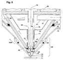
- FIG. 6 shows a detail of an objective lens, as known per se from EP 0767482 (FIG. 1).
- This objective lens can be operated both with the lens pole 62 having an axial pole gap, and with the single-pole lens lying outside the region shown in FIG. 6, whose inner pole piece 58 extends close to the sample.
- the detection in Fig. 6 takes place in the area between the pole piece 58 and the lens 62 , which is shielded from the magnetic fields of the two objective lenses.
- the signal is forwarded by means of a light guide through a hole in the pole piece 58 to be amplified outside the range shown by a photomultiplier.
- the electric field strength above the pressure stage diaphragm 18 can be freely selected in the design according to FIGS. 6 and 7 in wide ranges. It can be much lower than in the design according to FIGS. 2 to 5 with a combined electrostatic and magnetic objective lens and can also disappear completely, as in FIG. 6, in which the two pressure stage apertures 18 and 44 are at the same potential.
- FIG. 6 no electrode is provided above the lower pressure stage aperture 18 , which in contrast is at a positive potential.
- a further improved detection efficiency compared with FIG. 6 is obtained with a modification of the exemplary embodiment illustrated in FIG. 6, in which the upper pressure stage diaphragm 44 is at a positive potential with respect to the lower pressure stage diaphragm 18 .
- the upper pressure step diaphragm can then be advantageously contacted via the pole piece 58 or via the electrode 67, and the component 19 has a smaller structural height and a larger outer diameter and contains insulation.
- the primary electron beam extends in the vicinity of the optical axis 79 in FIG. 6 and is focused onto the sample 11 by the magnetic field of the lens 62 having an axial pole gap and / or by the magnetic field of the one-pole lens.
- the path of the primary electron beam through the opening of the pressure stage aperture 18 to the sample 11, the voltage between the sample 11 and the pressure stage aperture 18 and the movement of the secondary electrons from the sample 11 to the opening of the pressure stage aperture 18 in Fig. 6 the same as in Fig. 2 at Using the Einpollinse 64. The difference is that in Fig.
- the preferred voltage between the sample and the pressure stage diaphragm in Fig. 6 in excited single-pole operation is a few volts to a few hundred volts.
- a lower likelihood of scattering, a lower average scattering angle and a more forwardly directed angular distribution of the direction of movement are obtained, for example, by applying a voltage of 20 volts.
- voltages up to several hundred volts may also be advantageous, depending on the sample tilting and magnification, because under the conditions of the above example a weak secondary electron cascade would then arise.
- the amplification factor would be completely inadequate in connection with a collector electrode or a gas scintillation detector, in connection with the high-sensitivity detector 51 it represents an additional gain which, due to the broader energy distribution, slightly reduces the proportion of secondary electrons reaching the detector 51 , depending on the design of the detector, can overcompensate.
- the gas flowing in through the opening 16 from the sample chamber is pumped out through the side openings 20 and the tube 31 .
- the secondary electrons are forced on spiral paths where they pass through the upper pressure stage aperture 41 .
- the preferred size of the apertures of the pressure stage apertures 18 and 44 is dependent upon the desired maximum allowable pressure in the sample chamber, the desired minimum usable primary energy, and the quality of the vacuum that the cathode requires. It is possible to insert 44 further pressure stage diaphragms above the pressure stage diaphragm and to evacuate the resulting gaps.
- the preferred diameters of the openings of the pressure stage apertures 18 and 44 are the same as in FIG. 2, but the opening 41 may also be smaller than the opening of the lower pressure stage aperture 18 . Because the magnetic flux density generated by the Einpollinse is substantially larger in the upper Druckmaschinenblendenö réelle 41 (and the Larmorradius of the secondary electrons is much smaller) than in the opening of the lower pressure stage aperture 18.
- FIG. 6 In order to illustrate the qualitative course of the magnetic fields, two magnetic field lines from the sample to the interior of the detector housing 72 are shown in FIG. 6 by way of example. Above the pressure stage aperture 41 , the magnetic field strength decreases sharply. The strong magnetic field of the Einpollinse is replaced by the much weaker magnetic field of the cylindrical coils 66 and 71 , which continues to conduct the secondary electrons upwards. The symmetry axis of these magnetic fields coincides with the optical axis.
- a counter electrode 78 which can be placed opposite the detector housing 72 to negative potential and with which the secondary electrons, depending on the applied voltage between the sample 11 and the pressure level stop 18, braked in the direction of the optical axis and in the direction of Wire net 75 can be steered.
- the secondary electrons are directed by the magnetic field 80 generated by the coil 71 above the cylindrical coil 71 to the wire mesh 75 .
- the secondary electrons enter the detector housing 72 through the wire mesh 75 .
- On the other side of the wire mesh there is a strong electric field that accelerates the secondary electrons to the detector 51 , where they are detected.
- the preferred voltage between the wire mesh 75 and the detector 51 is 1 to 10 kV.
- a detector 51 for example, a semiconductor detector or, as shown in Fig. 6, a scintillator can be used.
- the use of such a highly sensitive secondary electron detector whose high voltage in the gas pressure of the sample chamber would inevitably lead to flashovers, is the reason for the much better signal-to-noise ratio, with the embodiment shown in Fig. 6 in comparison to the previously known Scanning electron microscopes with gas in the sample chamber is obtained.
- the space above the pressure stage aperture 44 is pumped out by the space between the cylindrical coils, which can also be divided into more than two parts, and then by the additional holes provided for electron-optical reasons anyway 38 .
- the tube 32, through which it is pumped out, opens into a component which is sealed against the pole piece by the seal 33 .
- FIG. 6 A great structural simplification in FIG. 6 can be achieved by omitting the component 25 , the tube 31, the lower pressure stage diaphragm 18 and the part of the component 19 which becomes unnecessary as a result. At the same pressure in the sample chamber, however, only one operation with a much smaller pressure stage aperture 41 is possible.
- EDX energy dispersive X-ray spectroscopy
- Fig. 6 or its above modification with an additional voltage between the two pressure stage apertures
- Fig. 7 is in the sample chamber outside the range shown in the direction of labeled with "EDX" Arrow attached an EDX detector.
- a header 26 without a collector electrode 13 is preferably used to enable EDX detection at a small distance between the pressure stage aperture 18 and the sample 11 .
- the distance between the Dmckhandnblende 18 and the sample 11 is preferably greater for EDX than the diameter of the opening of the Drucklienblende 18 and less than 1.5 millimeters.
- Between the pressure stage diaphragm and the sample is a voltage of preferably 50 to several 100 volts, for example of 300 volts.
- the gas pressure in the sample chamber is chosen so high that charges are compensated by the gas ions generated by the accelerated secondary electrons.
- the use of a small distance between the sample and the pressure stage aperture and a correspondingly higher gas pressure has the advantage that the gas ions reach the sample much more targeted where the charges are generated.
- the reduced primary electron scattering and the associated reduced signal from surrounding sample sites greatly improves the detection sensitivity in the EDX spectra.
- the primary energy can be reduced and thus the spatial resolution for the EDX spectra can be improved.
- the greatest disadvantages of today's EDX spectra are reduced with gas in the sample chamber.
- FIGS. 1 to 3 For the case of charge control on a flat sample which does not have to be tilted, for example in the case of metrology devices in semiconductor production, a modification of the exemplary embodiments shown in FIGS. 1 to 3 represents a preferred embodiment.
- both pressure stage apertures 18 and 18 are shown 44 even and between the pressure step diaphragms as well as between the lower pressure level diaphragm 18 and the sample 11 is applied to a homogeneous electric field.
- the lens 62 may be omitted, the inner pole piece 58 of the one-pole lens 64 is pulled far down so that the electric field between the electrode 55 and the pole piece 58 forms the electrostatic lens.
- the advantage of this embodiment in addition to the ease of manufacture in particular in the relatively low demands on the centerability of the two Druckstafenblenden, so that no device for centering the lower pressure level aperture 18 is required.
- the upper pressure step aperture 44 is arranged close to the lower edge of the pole piece 58 , for example at the height at which the maximum magnetic flux density prevails on the optical axis.
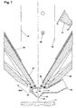
- FIG. 7 shows another exemplary embodiment of a pressure SEM according to the invention with only a magnetic objective lens, which in this case only consists of the one-pole lens 64 .
- the path of the primary electrons to the sample, the focusing of the primary electron beam by the one-pole lens 64 , the preferred size of the openings of the pressure stage apertures 18 and 44 , and the preferred voltage between the sample 11 and the lower pressure stage aperture 18 are the same as in FIG It should be noted, however, that tension between the sample and the lower pressure stage orifice is equal to FIG. 7 corresponding to the modification of FIG. 6 in which the upper pressure stage orifice 44 is at a positive potential to the lower pressure stage orifice 18 .
- FIG. 7 shows another exemplary embodiment of a pressure SEM according to the invention with only a magnetic objective lens, which in this case only consists of the one-pole lens 64 .
- a low voltage of a few volts between the sample and the lower pressure stage aperture has the advantage that the secondary electrons have only a small velocity component perpendicular to the optical axis. This improves the detection efficiency in the later detection.
- the secondary electrons with an energy of only a few electron volts also have a very small Larmorradius, but have a larger average scattering angle than at higher energy. Whether the positive or negative effect predominates depends on the distance between the sample and the pressure stage aperture, the gas pressure, the primary energy and the diameter of the pressure stage aperture 16 .
- the preferred potential difference between the two pressure stage apertures 18 and 44 in Fig. 7 is between 5 V and 500 V.
- the course of the magnetic field and the voltage between the specimen 11 and the lower pressure stage aperture 18 is available for the voltage between the two pressure stage apertures 18 and 44 is a voltage limit from which secondary electrons are no longer forced to reverse by the magnetic flux density increasing upward, but nearly all of the secondary electrons that have passed through the lower pressure stage aperture 16 are also forced through the upper pressure stage aperture 41 reach.
- the energy supplied to the secondary electrons is an important consideration for the selection of the voltage between the pressure stage diaphragms.
- the voltage between the lower and the upper pressure stage aperture is chosen so large that the energy of the secondary electrons above the upper pressure stage aperture 44 is at least as large as the minimum energy required not to follow the magnetic field lines diverging there, but upwards in FIG Direction to fly to the detector.
- the counter electrode 78 which is at the average potential of the two electrodes 75 and 81 , the secondary electrons can then be decelerated again.
- the detector 51 with its strong suction field is located behind the grid electrode 75 .
- the secondary electrons are directed by the electric field between the electrodes 81 and 75 and by the magnetic field 80 to the grid electrode 75 .
- the force effects due to the magnetic field and the electric field cancel each other out and the two fields form a Wien filter.
- the compensates for the effect of the lower Wien filter for the primary electrons In order to produce a chromatic error even with a primary energy of less than 4 keV at a relatively strong excitation of this Wien filter - for example, for deflection of 20 eV secondary electrons, above the Wien filter a second, in contrast rotated by 180 ° Wienfilter arranged, the compensates for the effect of the lower Wien filter for the primary electrons.
- This additional upper filter need not be located immediately above the lower Wien filter, but may also be higher up in the column. His static magnetic field can be generated for example by a raster coil.
- the stronger excitation of the Wien filter, which directs the secondary electrons toward the detector compared to vacuum operation, is advantageous when a larger voltage is applied between the sample and the lower pressure stage aperture, because it then increases the detection efficiency.
- a larger voltage up to a voltage of several hundred volts may be advantageous depending on the operating conditions.
- a voltage of, for example, 100 V to 500 V at a large distance between the sample and the lower pressure stage diaphragm by a voltage of, for example, 100 V to 500 V, a secondary electron cascade can be generated, which leads to a very good detection efficiency is still obtained, if only a small proportion of the secondary electrons the lower pressure stage aperture 16 passes.
- the structure shown in Fig. 7 is also suitable for large working distances. The same applies to the embodiment of FIG. 6 and for its modification with a voltage between the two pressure stage diaphragms.
- the pre-amplification with the help of a secondary electron cascade the thus achieved good detection efficiency at a long working distance and the magnification of the field of view at a large working distance are not on the embodiment limited in Fig. 7, but in operation with a one-pole lens in the other Embodiments achieved.
- the field curvature created by the application of the voltage between the lower pressure port aperture and the sample in the region of the lower pressure stage aperture 16 appears uncritical to the resolution. Because of the relatively high energy of the secondary electrons and because of the strong excitation of the one-pole lens, it also appears uncritical for the detection efficiency. If, however, this field curvature within the lower pressure stage aperture 16 is to be suppressed, this is easily possible with an auxiliary electrode 13 , as illustrated in FIGS. 4 and 6. By placing the auxiliary electrode 13 at a positive potential with respect to the lower pressure stage aperture 18 , the electric field strength within the lower pressure stage aperture 16 can be made so small that it no longer interferes. The resulting low electric field region in front of the pressure stage aperture 16 also reduces the average secondary electron energy, which is positive for detection. The amplification factor of the secondary electron cascade is however somewhat weakened.
- the preferred voltage is 1 to 20 kV.
- the Druckstafenblende 44 in Fig. 6 and Fig. 7 is easily replaceable, so that it can be easily replaced.
- a high magnetic flux density prevails and the opening 41 is preferably so large that not only all the secondary electrons, but also most backscattered electrons that are not shaded by the lower pressure level orifice 18 , through the opening 41 get through.
- Another preferred variation of the embodiments of Figs. 6 and 7, which permits a particularly large diameter of the lower pressure stage aperture 16 is that the upper pressure stage aperture 41 is equal to or less than the lower pressure stage aperture 16.
- the upper pressure stage aperture 44 Near below the upper pressure stage aperture 44 is (with, for example, 100 microns, but at most 1 mm distance) mounted an additional aperture whose opening diameter is greater than or equal to the opening diameter of the upper pressure stage aperture 44.
- the space between the two diaphragms is connected to a controllable gas supply, for example, flows through the ozone .
- the partial pressure of the ozone at the location of the pressure stage aperture 41 differs from the partial pressure of the water vapor when operating with maximum allowed gas pressure in the sample chamber by a factor of less than 100, preferably by a factor of less than 20. If desirable, the upper Pressure stage aperture 44 are used in this embodiment simultaneously as an aperture diaphragm.
- the holder 19 of the upper pressure stage diaphragm is mounted in Fig. 7 easily removable on the electrode 67 , via which the pressure level aperture 44 is also contacted.
- the lower pressure level aperture 18 is easily removable mounted on the pole piece 58 .
- the intermediate space between the two pressure stage diaphragms is evacuated by means of a corrugated hose 63 which, for example, can be flanged easily removable in the sample chamber.
- the corrugated tube 63 impedes the sample tiltability only in one direction, so that the sample can be tilted in all directions, if it is previously rotated accordingly.
- FIG. 7 An advantageous modification of Fig. 7 is that below the sample another Einpollinse 64 is arranged with upwardly open Polschuhspalt, as is known from scanning transmission electron microscopes or scanning electron microscopes with "in-lens operation".
- the advantage besides reduced error coefficients, is mainly an increased magnetic flux density at the location of the sample. This ensures that even at the same potential of the two pressure stage apertures 18 and 44, only very few secondary electrons are forced to reverse by the increasing magnetic flux density.
- a preferred embodiment in connection therewith, therefore, is that the two pressure stage diaphragms are part of a common insert 26 , as in FIG.
- Another preferred modification of the embodiment shown in Fig. 7 is that the detection below the counter electrode 78 takes place through a hole in the pole piece 58 through which the suction field of the detector 51 attracts the secondary electrons. In this case, no additional magnetic field 80 is required.
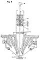
- Fig. 1 only those secondary electrons are detected, which have a sufficiently large distance from the optical axis 79 when reaching the detector 74 so as not to fly through the opening 77 of the detector. The remaining secondary electrons fly through the opening 77 of the detector.
- these secondary electrons 86 are also detected in the embodiment of FIG.
- an additional upper detector 91 is used, which is mounted close below the aperture stop 94 .
- the electrode 55 is extended upwards beyond the aperture stop, and the aperture stop 94 and the detector 91 are at the potential of the electrode 55. Due to the small size, for example, the use of a semiconductor detector (with downstream optocoupler) as the upper detector 91 is advantageous.
- the lower detector 74 and the aperture stop 94 are also used as pressure step apertures at the same time. Between the pressure stage apertures 44 , 74 and 94 and above the pressure stage aperture 94 is pumped through the openings 73, 76 and 98 , as indicated by the arrows.
- an electromagnetic aperture changer is advantageous because the aperture stop then does not need to be movable.
- FIG. 9 shows another variant of a pressure SEM according to the invention with an additional upper detector 91 , which is embodied here as a combination with the aperture stop 94 .
- a preferred embodiment is the use of semiconductor material for the combined component, wherein the semiconductor material may be etched away in the region around the optical axis 79 to a small thickness ( ⁇ 100 microns), so that the aperture apertures have only a small length. From above, a metal coating is applied, which acts as an aperture stop 94 and from below, the combined component is designed as a semiconductor detector 91 .
- a preferred embodiment is that ultra-high vacuum prevails above the aperture stop 94 so that the aperture stop does not need to be heated.
- the primary electron beam emitted from the cathode 99 is threaded through the desired opening of the aperture stop 94 by means of an electromagnetic aperture changer.
- the primary electron beam 82 is directed by the magnetic fields 83 and 80 back to the optical axis.
- the subsequent path is the same for the primary and secondary electrons as in FIG. 1.
- the secondary electrons 85 (and low energy loss backscattered electrons) along the optical axis through the lower detector aperture 77 become fly, deflected by the magnetic fields 80 and 83 from the optical axis and directed to the upper detector 91 .
- the additional upper detector 91 shown in FIGS. 8 and 9 may be combined with the embodiments of FIGS. 2 to 5 as well as with any particle beam apparatus in which the primary corpuscular beam passes close to the edge of the detector 74 (eg through an aperture 77) the detector) and in which there is an electric field between the sample 11 and the detector 74 which accelerates the secondary particles towards the detector 74 .
- the detection of the secondary electrons or secondary corpuscles that have flown past the edge of the lower detector 47 causes an increase in the detection efficiency both when operating with gas in the sample chamber and during vacuum operation.
- the additional upper detector 91 When operating with vacuum in the sample chamber without the pressure stage apertures 18 and 44 , the additional upper detector 91 provides a great improvement in detection efficiency when the secondary electrons are focused under unfavorable operating conditions on the opening 77 of the lower detector. Furthermore, the improvement of the detection efficiency for the image center of low magnification images is positively noticeable.
- the detector 91 can be divided into a plurality of particle-sensitive regions, which can be arranged concentrically to the optical axis, for example. The same advantages are also obtained when using the additional upper detector in a particle beam device.
- the electrodes 18, 25, 44 (or 39 and 43 in FIGS. 3 and 5), 50 and 55 are all set to the same potential.
- a collector electrode detector (WO 88/09564 A1, WO 90/04261 A1) or a gas scintillation detector and for operation with vacuum in the sample chamber, a laterally arranged Everhardt-Thornley detector is used.
- the collector electrode used is the pressure stage diaphragm 18 and / or a collector electrode 13 which is insulated in contrast thereto , as shown, for example, in FIG. 4. With the collector electrode detector, for which prevail at the large distance between the sample 11 and the pressure level diaphragm 18 favorable operating conditions, then at least the same signal-to-noise ratio is achieved as in the currently known pressure-SEMs.
- An advantageous embodiment of the pressure SEMs according to the invention which causes a large increase in the field of view at a large distance between the sample 11 and the pressure level aperture 18 , is that instead of the deflection coils 59, a double baffle is used.
- the position of the raster center on the optical axis can be freely selected.
- the greatest possible field of view is achieved when scanning is effected around a point between the two pressure stage apertures 18 and 44 whose position on the optical axis 79 is selected so that the field of view is limited both by the lower pressure stage aperture 18 and the overlying pressure stage aperture 44 ,
- a preferred embodiment is the combination with a computer-controlled sample stage and image processing, which makes it possible to assemble several electron microscopic individual images into a larger overall image.
- Another preferred embodiment consists in the integration of an incident-light microscope or a confocal laser microscope into the sample chamber.
- an overview image is taken before the examination with the electron beam from the sample already mounted on the sample table and stored by the computer.
- points can be marked with the help of the computer, which are then approached by the computer-controlled sample stage for scanning electron microscopic examination.
- Such light microscopic overview images make scanning electron microscopic overview images in the pressure SEM superfluous for most applications.
- the working distance from the computer can be adjusted during the subsequent examination with the electron beam without additional distance control and, when the sample table is moved, contact between the sample 11 and the pressure level aperture 18 can be safely avoided.
Landscapes
- Chemical & Material Sciences (AREA)
- Analytical Chemistry (AREA)
- Analysing Materials By The Use Of Radiation (AREA)
Claims (22)
- Microscope électronique à balayage comprenant un canon électronique et une chambre d'échantillon, entre lesquels est(sont) disposé(s) un ou plusieurs diaphragme(s) de palier atmosphérique, à travers les ouvertures duquel(desquels) un faisceau électronique primaire peut être dirigé sur un échantillon dans la chambre d'échantillon et comprenant une lentille magnétique, avec laquelle le faisceau électronique primaire sur l'échantillon peut être mis au point, le diaphragme de palier atmosphérique (18) le plus inférieur, le plus proche de l'échantillon, à travers lequel le faisceau électronique primaire touche l'échantillon, étant réglé pour isoler une pression plus élevée dans la chambre d'échantillon par rapport au reste de la colonne du microscope électronique à balayage et pour faire passer des électrons secondaires à travers son ouverture (16) depuis l'échantillon jusqu'à au moins un détecteur,
caractérisé en ce que
le détecteur est disposé côté canon électronique par le champ magnétique de la lentille magnétique effectuant la mise au point et est un détecteur polarisé de façon positive par rapport à l'échantillon et comprend une multiplication du signal, de telle sorte qu'une pluralité de photons, d'électrons ou de paires électron-trou est générée par chaque électron secondaire dans le détecteur, le détecteur comportant une combinaison de scintillateur et de photomultiplicateur, un détecteur semi-conducteur, un détecteur channelplate ou un détecteur channeltron. - Microscope électronique à balayage selon la revendication 1, dans lequel au moins une électrode (39, 43, 44, 55) est disposée au-dessus du diaphragme de palier atmosphérique le plus inférieur (18), laquelle électrode présente par rapport au diaphragme de palier atmosphérique (18) une tension positive et est réglée pour diriger les électrons secondaires de l'échantillon au détecteur (51, 74, 91).
- Microscope électronique à balayage selon la revendication 1, qui est réglé pour détecter des électrons secondaires à travers l'ouverture d'au moins un diaphragme de palier atmosphérique, qui est constitué par couches d'au moins deux couches (39, 43) conductrices, isolées électriquement l'une de l'autre, les couches conductrices pouvant être alimentées en tensions, de telle sorte que le côté inférieur ou supérieur du diaphragme de palier atmosphérique respectif possède une tension aux électrodes.
- Microscope électronique à balayage selon la revendication 2 ou 3, dans lequel le diaphragme de palier atmosphérique (18) et/ou les électrodes situées sur celui-ci (39, 43, 44, 50, 55) forment une ou plusieurs lentille(s) électrostatique(s) qui est(sont) réglée(s) pour faire la mise au point du faisceau électronique primaire dans le champ électrique entre le diaphragme de palier atmosphérique (18) et l'électrode située sur celui-ci (44 et/ou 39) et/ou entre les électrodes situées sur celui-ci (43, 44, 50, 55).
- Microscope électronique à balayage selon la revendication 2 ou 3, dans lequel les électrodes (39, 43, 44, 50, 55) sont disposées de façon concentrique par rapport à l'axe optique du microscope électronique à balayage.
- Microscope électronique à balayage selon l'une des revendications 2 à 5, dans lequel la surface du détecteur (51, 75, 91) présente au moins dans des plages partielles une tension qui est positive de plus de 500 V par rapport à la tension de l'échantillon.
- Microscope électronique à balayage selon l'une des revendications 2 à 5, dans lequel la surface du détecteur (51, 75, 91) présente au moins dans des plages partielles une tension qui est positive de plus de 1000 V par rapport à la tension de l'échantillon.
- Microscope électronique à balayage selon l'une des revendications 2 à 7, dans lequel est prévue une lentille d'objectif électrostatique et magnétique combinée.
- Microscope électronique à balayage selon l'une des revendications 2 à 8, dans lequel une ou plusieurs électrode(s) (39, 44) forme(nt) au-dessus du diaphragme de palier atmosphérique (18) d'autres diaphragmes de palier atmosphérique, des systèmes de pompe destinés à générer des dépressions dans les espaces intermédiaires situés entre les diaphragmes de palier atmosphérique étant prévus.
- Microscope électronique à balayage selon la revendication 9, dans lequel les électrodes configurées comme des diaphragmes de palier atmosphérique possèdent des ouvertures qui possèdent une dimension caractéristique inférieure à 1500 µm.
- Microscope électronique à balayage selon l'une des revendications 2 à 10, dans lequel est prévue une structure constituante, les composants (13, 18, 19, 31, 32, 39, 40, 42 à 44, 60, 63, 65, 68, 69) nécessaires au fonctionnement du microscope dans le cas d'une pression plus élevée dans la chambre d'échantillon formant dans la chambre d'échantillon un ou plusieurs sous-groupe facilement démontable(s).
- Microscope électronique à balayage selon la revendication 2, dans lequel un premier détecteur (74) est disposé avec son bord extérieur ou une ouverture intérieure (77) de manière adjacente au faisceau électronique primaire et un second détecteur (91) est prévu, qui est positionné par rapport à la direction de déplacement des électrons secondaires derrière le bord et/ou l'ouverture du premier détecteur (74) et réglé pour détecter des électrons secondaires (85, 86) qui se déplacent sur le bord en passant devant une ouverture (77) ou à travers celle-ci.
- Microscope électronique à balayage selon l'une des revendications 2 à 12, dans lequel les électrons secondaires sont déviés de l'axe optique à l'aide d'un champ magnétique (80).
- Microscope électronique à balayage selon la revendication 1, dans lequel la surface du détecteur (51, 75, 91) présente au moins dans des plages partielles une tension qui est positive de plus de 500 V par rapport à la tension de l'échantillon.
- Microscope électronique à balayage selon la revendication 1, dans lequel la surface du détecteur (51, 75, 91) présente au moins dans des plages partielles une tension qui est positive de plus de 1000 V par rapport à la tension de l'échantillon.
- Microscope électronique à balayage selon la revendication 1 ou 15, dans lequel est prévue une structure constituante, les composants (13, 18, 19, 26, 31, 32, 39, 40, 42 à 44, 60, 63, 65, 68, 69) à présent nécessaires au fonctionnement du microscope dans le cas d'une pression plus élevée dans la chambre d'échantillon formant dans la chambre d'échantillon un ou plusieurs sous-groupe facilement démontable(s).
- Microscope électronique à balayage selon l'une quelconque des revendications précédentes, dans lequel est présent un champ magnétique entre l'échantillon (11) et le diaphragme de palier atmosphérique le plus inférieur (18), qui est à symétrie de révolution par rapport à l'axe optique et qui améliore le transport des électrons secondaires de l'échantillon à l'ouverture de diaphragme de palier atmosphérique (16).
- Microscope électronique à balayage selon l'une quelconque des revendications précédentes, dans lequel les électrons secondaires cheminent en direction du détecteur (51, 74, 91) à travers au moins deux ouvertures de diaphragme de palier atmosphérique (16, 41), dans lesquelles est présent un champ magnétique de telle sorte que l'ensemble des lignes de force du champ magnétique, qui s'étendent à travers l'ouverture inférieure de diaphragme de palier atmosphérique (18), s'étend également à travers l'ouverture supérieure de diaphragme de palier atmosphérique (44).
- Microscope électronique à balayage selon l'une quelconque des revendications précédentes, dans lequel est aménagé un champ magnétique additionnel (80) en plus du champ magnétique de la lentille d'objectif (62, 64), lequel champ magnétique dirige les électrons secondaires en direction du détecteur (51).
- Microscope électronique à balayage selon l'une quelconque des revendications précédentes, dans lequel une contre-électrode (78) est réglée pour freiner les électrons secondaires et favoriser de ce fait le transport des électrons secondaires en direction du détecteur (51).
- Microscope électronique à balayage selon l'une quelconque des revendications précédentes, dans lequel un détecteur est prévu pour une spectrométrie X à dispersion d'énergie (EDX) pour fonctionner sur des distances inférieures à 1,5 mm entre l'échantillon (11) et le diaphragme de palier atmosphérique le plus inférieur (18).
- Procédé d'enregistrement d'images d'un échantillon prises par un microscope électronique à balayage, comprenant les étapes de :disposition de l'échantillon dans une chambre d'échantillon sous une pression plus élevée,irradiation de l'échantillon par un faisceau électronique primaire, qui est généré par un canon électronique, un ou plusieurs diaphragme(s) de palier atmosphérique et une lentille magnétique destinée à faire la mise au point du faisceau électronique primaire sur l'échantillon étant disposés entre le canon électronique et l'échantillon,transport des électrons secondaires à travers l'un des diaphragmes de palier atmosphérique en direction d'un détecteur (51, 74, 91) polarisé de façon positive, qui est disposé côté canon électronique par le champ magnétique de la lentille magnétique effectuant une mise au point, le détecteur comportant une combinaison de scintillateur et de photomultiplicateur, un détecteur de semi-conducteur, un détecteur de channelplate ou un détecteur de channeltron,multiplication du signal dans le détecteur ou le long de la surface du détecteur, une pluralité de photons, d'électrons ou de paires d'électron-trou étant générée par chaque électron secondaire, etdétermination de l'image prise par le microscope électronique à balayage à partir du signal du détecteur.
Applications Claiming Priority (5)
| Application Number | Priority Date | Filing Date | Title |
|---|---|---|---|
| DE19810301 | 1998-03-10 | ||
| DE19810301 | 1998-03-10 | ||
| DE19845329 | 1998-10-01 | ||
| DE19845329A DE19845329C2 (de) | 1998-03-10 | 1998-10-01 | Rasterelektronenmikroskop |
| PCT/EP1999/001544 WO1999046797A1 (fr) | 1998-03-10 | 1999-03-10 | Microscope electronique a balayage |
Publications (2)
| Publication Number | Publication Date |
|---|---|
| EP1068630A1 EP1068630A1 (fr) | 2001-01-17 |
| EP1068630B1 true EP1068630B1 (fr) | 2005-07-20 |
Family
ID=26044511
Family Applications (1)
| Application Number | Title | Priority Date | Filing Date |
|---|---|---|---|
| EP99914503A Expired - Lifetime EP1068630B1 (fr) | 1998-03-10 | 1999-03-10 | Microscope electronique a balayage |
Country Status (4)
| Country | Link |
|---|---|
| US (1) | US6590210B1 (fr) |
| EP (1) | EP1068630B1 (fr) |
| JP (1) | JP2002507045A (fr) |
| WO (1) | WO1999046797A1 (fr) |
Cited By (1)
| Publication number | Priority date | Publication date | Assignee | Title |
|---|---|---|---|---|
| US10068744B2 (en) | 2015-12-01 | 2018-09-04 | Carl Zeiss Microscopy Gmbh | Charged particle optical apparatus for through-the lens detection of particles |
Families Citing this family (56)
| Publication number | Priority date | Publication date | Assignee | Title |
|---|---|---|---|---|
| DE19828476A1 (de) * | 1998-06-26 | 1999-12-30 | Leo Elektronenmikroskopie Gmbh | Teilchenstrahlgerät |
| JP5143990B2 (ja) * | 2000-07-07 | 2013-02-13 | カール・ツァイス・エヌティーエス・ゲーエムベーハー | 変化する圧力領域のための検出器、およびこのような検出器を備える電子顕微鏡 |
| GB2367686B (en) * | 2000-08-10 | 2002-12-11 | Leo Electron Microscopy Ltd | Improvements in or relating to particle detectors |
| DE10061798A1 (de) * | 2000-12-12 | 2002-06-13 | Leo Elektronenmikroskopie Gmbh | Monochromator für geladene Teilchen |
| GB2374723B (en) * | 2001-04-20 | 2005-04-20 | Leo Electron Microscopy Ltd | Scanning electron microscope |
| US20050103272A1 (en) * | 2002-02-25 | 2005-05-19 | Leo Elektronenmikroskopie Gmbh | Material processing system and method |
| US6674075B2 (en) * | 2002-05-13 | 2004-01-06 | Applied Materials, Inc. | Charged particle beam apparatus and method for inspecting samples |
| DE10233002B4 (de) * | 2002-07-19 | 2006-05-04 | Leo Elektronenmikroskopie Gmbh | Objektivlinse für ein Elektronenmikroskopiesystem und Elektronenmikroskopiesystem |
| US7504182B2 (en) * | 2002-09-18 | 2009-03-17 | Fei Company | Photolithography mask repair |
| US6979822B1 (en) * | 2002-09-18 | 2005-12-27 | Fei Company | Charged particle beam system |
| US6825475B2 (en) * | 2002-09-19 | 2004-11-30 | Applied Materials Israel, Ltd. | Deflection method and system for use in a charged particle beam column |
| US6674076B1 (en) * | 2002-12-12 | 2004-01-06 | Ballard Power Systems Inc. | Humidified imaging with an environmental scanning electron microscope |
| DE10301579A1 (de) * | 2003-01-16 | 2004-07-29 | Leo Elektronenmikroskopie Gmbh | Elektronenstrahlgerät und Detektoranordnung |
| US6897442B2 (en) * | 2003-04-25 | 2005-05-24 | Applied Materials Israel, Ltd. | Objective lens arrangement for use in a charged particle beam column |
| JP4073839B2 (ja) * | 2003-07-22 | 2008-04-09 | 株式会社神戸製鋼所 | 分析装置用磁場発生装置 |
| KR101041661B1 (ko) | 2003-07-30 | 2011-06-14 | 어플라이드 머티리얼즈 이스라엘 리미티드 | 다중 검출기들을 갖는 스캐닝 전자 현미경 및 다중 검출기기반 이미징을 위한 방법 |
| PL207238B1 (pl) * | 2003-10-14 | 2010-11-30 | Politechnika Wroclawska | Układ detekcyjny elektronów wtórnych i wstecznie rozproszonych do skaningowego mikroskopu elektronowego |
| US7842933B2 (en) | 2003-10-22 | 2010-11-30 | Applied Materials Israel, Ltd. | System and method for measuring overlay errors |
| US7531812B2 (en) * | 2003-10-27 | 2009-05-12 | Politechnika Wroclawska | Method and system for the directional detection of electrons in a scanning electron microscope |
| PL208151B1 (pl) * | 2003-10-27 | 2011-03-31 | Politechnika Wroclawska | Układ do detekcji elektronów w skaningowym mikroskopie elektronowym |
| DE602004031817D1 (de) * | 2004-01-21 | 2011-04-28 | Integrated Circuit Testing | Strahlenoptische Komponente mit einer teilchenoptischen Linse |
| US7112803B2 (en) * | 2004-07-23 | 2006-09-26 | Applied Materials, Israel, Ltd. | Beam directing system and method for use in a charged particle beam column |
| DE102004037781A1 (de) * | 2004-08-03 | 2006-02-23 | Carl Zeiss Nts Gmbh | Elektronenstrahlgerät |
| TW200639901A (en) * | 2005-05-09 | 2006-11-16 | Li Bing Huan | Device for operating gas in vacuum or low-pressure environment and for observation of the operation |
| EP2211368B1 (fr) * | 2005-11-28 | 2012-06-27 | Carl Zeiss SMT GmbH | Composant optique corpusculaire |
| JP4601545B2 (ja) * | 2005-12-02 | 2010-12-22 | 株式会社神戸製鋼所 | 平行磁場型ラザフォード後方散乱イオン測定装置 |
| JP4597077B2 (ja) * | 2006-03-14 | 2010-12-15 | 株式会社日立ハイテクノロジーズ | 走査電子顕微鏡 |
| JP5053359B2 (ja) * | 2006-03-31 | 2012-10-17 | エフ・イ−・アイ・カンパニー | 荷電粒子ビーム器具用の改善された検出器 |
| DE102006043895B9 (de) * | 2006-09-19 | 2012-02-09 | Carl Zeiss Nts Gmbh | Elektronenmikroskop zum Inspizieren und Bearbeiten eines Objekts mit miniaturisierten Strukturen |
| EP1916696B1 (fr) * | 2006-10-25 | 2017-04-19 | ICT, Integrated Circuit Testing Gesellschaft für Halbleiterprüftechnik mbH | Détecteur pour particules chargées, appareil des particules chargées et méthode de formation d'une image |
| DE102007010873B4 (de) * | 2007-03-06 | 2009-07-30 | Carl Zeiss Nts Gmbh | Objektivlinse |
| JP4977509B2 (ja) * | 2007-03-26 | 2012-07-18 | 株式会社日立ハイテクノロジーズ | 走査電子顕微鏡 |
| US7791020B2 (en) * | 2008-03-31 | 2010-09-07 | Fei Company | Multistage gas cascade amplifier |
| PL217173B1 (pl) * | 2008-07-14 | 2014-06-30 | Politechnika Wroclawska | Układ detekcyjny elektronów i skaningowy mikroskop elektronowy |
| US8299432B2 (en) * | 2008-11-04 | 2012-10-30 | Fei Company | Scanning transmission electron microscope using gas amplification |
| US8334511B2 (en) * | 2009-05-15 | 2012-12-18 | Fei Company | Electron microscope with integrated detector(s) |
| US20110006205A1 (en) * | 2009-07-12 | 2011-01-13 | Raymond Browning | Ambient pressure photoelectron microscope |
| DE102009041993B4 (de) | 2009-09-18 | 2020-02-13 | Carl Zeiss Microscopy Gmbh | Beobachtungs- und Analysegerät |
| US9046475B2 (en) | 2011-05-19 | 2015-06-02 | Applied Materials Israel, Ltd. | High electron energy based overlay error measurement methods and systems |
| US8653443B2 (en) * | 2011-06-29 | 2014-02-18 | Philip James Witham | Neutral particle microscope |
| EP2706554B1 (fr) * | 2012-09-10 | 2016-05-25 | Fei Company | Procédé d'utilisation de lentille combinée à particules chargées |
| EP2950324B1 (fr) * | 2014-05-28 | 2018-11-21 | Carl Zeiss Microscopy GmbH | Appareil optique à particules chargées ayant un module de pression différentielle pouvant être positionné sélectivement |
| US9478390B2 (en) * | 2014-06-30 | 2016-10-25 | Fei Company | Integrated light optics and gas delivery in a charged particle lens |
| JP2016051593A (ja) * | 2014-08-29 | 2016-04-11 | 株式会社ホロン | リターディング電圧を用いた荷電粒子線装置 |
| JP6548374B2 (ja) * | 2014-09-22 | 2019-07-24 | 株式会社ホロン | 低真空用荷電粒子線装置 |
| US10008360B2 (en) | 2015-01-26 | 2018-06-26 | Hermes Microvision Inc. | Objective lens system for fast scanning large FOV |
| AU2016309960B2 (en) * | 2015-08-18 | 2020-11-05 | Danilatos, Gerasimos Daniel DR | Wide field atmospheric scanning electron microscope |
| US9972474B2 (en) | 2016-07-31 | 2018-05-15 | Fei Company | Electron microscope with multiple types of integrated x-ray detectors arranged in an array |
| JP2018181790A (ja) * | 2017-04-21 | 2018-11-15 | 株式会社ホロン | 走査型電子顕微鏡および走査型電子顕微鏡の2次電子検出方法 |
| JP7313499B2 (ja) * | 2017-04-21 | 2023-07-24 | 株式会社ホロン | 走査型電子顕微鏡および走査型電子顕微鏡の2次電子検出方法 |
| EP3477390A1 (fr) * | 2017-10-25 | 2019-05-01 | ASML Netherlands B.V. | Outil d'inspection, appareil lithographique, source de faisceau d'électrons et procédé d'inspection |
| US11264198B2 (en) * | 2018-10-15 | 2022-03-01 | Applied Materials Israel Ltd. | Objective lens arrangement |
| DE102018131614B3 (de) * | 2018-12-10 | 2020-02-06 | Carl Zeiss Microscopy Gmbh | Partikelstrahlsystem und Verfahren zum Betreiben eines Partikelstrahlsystems |
| JP6815437B2 (ja) * | 2019-04-26 | 2021-01-20 | 株式会社ホロン | 低真空用荷電粒子線装置 |
| US11508591B2 (en) * | 2021-02-08 | 2022-11-22 | Kla Corporation | High resolution electron beam apparatus with dual-aperture schemes |
| WO2023237277A1 (fr) * | 2022-06-10 | 2023-12-14 | Asml Netherlands B.V. | Appareil à faisceau de particules chargées avec correction rapide de la mise au point et procédés associés |
Family Cites Families (20)
| Publication number | Priority date | Publication date | Assignee | Title |
|---|---|---|---|---|
| DE3638682A1 (de) | 1986-11-13 | 1988-05-19 | Siemens Ag | Spektrometerobjektiv fuer korpuskularstrahlmesstechnik |
| DE3703028A1 (de) | 1987-02-02 | 1988-09-01 | Siemens Ag | Rastermikroskop |
| US4823006A (en) * | 1987-05-21 | 1989-04-18 | Electroscan Corporation | Integrated electron optical/differential pumping/imaging signal detection system for an environmental scanning electron microscope |
| US4785182A (en) | 1987-05-21 | 1988-11-15 | Electroscan Corporation | Secondary electron detector for use in a gaseous atmosphere |
| US4897545A (en) * | 1987-05-21 | 1990-01-30 | Electroscan Corporation | Electron detector for use in a gaseous environment |
| EP0548573B1 (fr) | 1991-11-27 | 1998-02-25 | Hitachi, Ltd. | Appareil à faisceau d'électrons |
| US5396067A (en) | 1992-06-11 | 1995-03-07 | Nikon Corporation | Scan type electron microscope |
| JP3081393B2 (ja) * | 1992-10-15 | 2000-08-28 | 株式会社日立製作所 | 走査電子顕微鏡 |
| DE4236273A1 (en) | 1992-10-27 | 1993-07-01 | Siemens Ag | Lens for focussing electrons for specimen inspection - has field generated by coils and cone-shaped electrode set into entry section |
| US5362964A (en) | 1993-07-30 | 1994-11-08 | Electroscan Corporation | Environmental scanning electron microscope |
| US5412211A (en) | 1993-07-30 | 1995-05-02 | Electroscan Corporation | Environmental scanning electron microscope |
| JP3291880B2 (ja) * | 1993-12-28 | 2002-06-17 | 株式会社日立製作所 | 走査形電子顕微鏡 |
| EP0708975B1 (fr) | 1994-04-12 | 1997-12-03 | Koninklijke Philips Electronics N.V. | Appareil d'optique particulaire comportant un detecteur d'electrons secondaires |
| JPH0868772A (ja) * | 1994-06-02 | 1996-03-12 | Kla Instr Corp | 電子ビーム・マイクロスコピーを用いた自動マスク検査装置及び方法 |
| DE69504294T2 (de) * | 1994-12-19 | 1999-04-08 | Opal Technologies Ltd | System zur Hochauflösungsbildgebung und Messung von topographischen Characteristiken und Materialcharakteristiken einer Probe |
| JP3323021B2 (ja) | 1994-12-28 | 2002-09-09 | 株式会社日立製作所 | 走査形電子顕微鏡及びそれを用いた試料像観察方法 |
| US5677531A (en) | 1995-08-08 | 1997-10-14 | Nikon Corporation | Scanning electron microscope |
| US6025592A (en) | 1995-08-11 | 2000-02-15 | Philips Electronics North America | High temperature specimen stage and detector for an environmental scanning electron microscope |
| DE19605855A1 (de) | 1996-02-16 | 1997-08-21 | Act Advanced Circuit Testing | Detektorobjektiv für Korpuskularstrahlgeräte |
| CZ284288B6 (cs) | 1997-03-13 | 1998-10-14 | Preciosa, A. S. | Detekční systém rastrovacího elektronového mikroskopu |
-
1999
- 1999-03-10 EP EP99914503A patent/EP1068630B1/fr not_active Expired - Lifetime
- 1999-03-10 WO PCT/EP1999/001544 patent/WO1999046797A1/fr active IP Right Grant
- 1999-03-10 US US09/623,824 patent/US6590210B1/en not_active Expired - Lifetime
- 1999-03-10 JP JP2000536092A patent/JP2002507045A/ja active Pending
Cited By (4)
| Publication number | Priority date | Publication date | Assignee | Title |
|---|---|---|---|---|
| US10068744B2 (en) | 2015-12-01 | 2018-09-04 | Carl Zeiss Microscopy Gmbh | Charged particle optical apparatus for through-the lens detection of particles |
| US10522321B2 (en) | 2015-12-01 | 2019-12-31 | Carl Zeiss Microscopy Gmbh | Charged particle optical apparatus for through-the-lens detection of particles |
| US10861670B2 (en) | 2015-12-01 | 2020-12-08 | Carl Zeiss Microscopy Gmbh | Charged particle optical apparatus for through-the-lens detection of particles |
| US11276547B2 (en) | 2015-12-01 | 2022-03-15 | Carl Zeiss Microscopy Gmbh | Charged particle optical apparatus for through-the-lens detection of particles |
Also Published As
| Publication number | Publication date |
|---|---|
| EP1068630A1 (fr) | 2001-01-17 |
| US6590210B1 (en) | 2003-07-08 |
| WO1999046797A1 (fr) | 1999-09-16 |
| JP2002507045A (ja) | 2002-03-05 |
Similar Documents
| Publication | Publication Date | Title |
|---|---|---|
| EP1068630B1 (fr) | Microscope electronique a balayage | |
| DE69332995T2 (de) | Raster-Elektronenmikroskop | |
| DE102006043895B4 (de) | Elektronenmikroskop zum Inspizieren und Bearbeiten eines Objekts mit miniaturisierten Strukturen | |
| DE10233002B4 (de) | Objektivlinse für ein Elektronenmikroskopiesystem und Elektronenmikroskopiesystem | |
| DE69937910T2 (de) | Gerät und Verfahren zur Probenuntersuchung mittels Ladungsträgerstrahlen | |
| DE60011031T2 (de) | Optische Säule für Teilchenstrahlvorrichtung | |
| EP1892748B1 (fr) | Système de traitement de matériau et procédé de traitement de matériau | |
| DE2235903C2 (de) | Verfahren zum Betrieb eines Feldemissions-Raster-Korpuskularstrahlmikroskops und Feldemissions-Raster-Korpuskularstrahlmikroskop zur Durchführung des Verfahrens | |
| DE69634032T2 (de) | Unter etwas erhöhtem druck arbeitendes feldemissionsrasterelektronenmikroskop | |
| EP0281743B1 (fr) | Objectif détecteur pour microscope à balayage | |
| DE102008040426B4 (de) | Verfahren zur Untersuchung einer Oberfläche eines Objekts | |
| DE102020125534B3 (de) | Vielzahl-Teilchenstrahlmikroskop und zugehöriges Verfahren mit schnellem Autofokus um einen einstellbaren Arbeitsabstand | |
| DE112014002951T5 (de) | Rasterelektronenmikroskop | |
| DE112016000644B4 (de) | Verbundvorrichtung für geladene Partikelstrahlen | |
| DE69920182T2 (de) | Korpuskularstrahloptisches gerät mit auger-elektronendetektion | |
| DE102007010873B4 (de) | Objektivlinse | |
| DE112015001235B4 (de) | Vorrichtung und verfahren zur abbildung mittels eines elektronenstrahls unter verwendung eines monochromators mit doppeltem wien-filter sowie monochromator | |
| DE69133256T2 (de) | Rasterelekronenmikroskop und Bilderzeugungsverfahren | |
| DE60105199T2 (de) | Sem mit einem sekundärelektronendetektor mit einer zentralelektrode | |
| DE102011087955A1 (de) | Raster-Elektronen-Mikroskop | |
| DE19845329C2 (de) | Rasterelektronenmikroskop | |
| DE2608958A1 (de) | Vorrichtung zum erzeugen von strahlen aus geladenen teilchen | |
| DE19953300A1 (de) | Instrument zum Detektieren von geladenen Teilchen | |
| DE19952169A1 (de) | Magnetische Linse | |
| DE102021105201A1 (de) | Vielzahl-Teilchenstrahlmikroskop und zugehöriges Verfahren mit schnellem Autofokus mit speziellen Ausführungen |
Legal Events
| Date | Code | Title | Description |
|---|---|---|---|
| PUAI | Public reference made under article 153(3) epc to a published international application that has entered the european phase |
Free format text: ORIGINAL CODE: 0009012 |
|
| 17P | Request for examination filed |
Effective date: 20000830 |
|
| AK | Designated contracting states |
Kind code of ref document: A1 Designated state(s): DE GB NL |
|
| 17Q | First examination report despatched |
Effective date: 20010521 |
|
| GRAP | Despatch of communication of intention to grant a patent |
Free format text: ORIGINAL CODE: EPIDOSNIGR1 |
|
| GRAS | Grant fee paid |
Free format text: ORIGINAL CODE: EPIDOSNIGR3 |
|
| GRAA | (expected) grant |
Free format text: ORIGINAL CODE: 0009210 |
|
| AK | Designated contracting states |
Kind code of ref document: B1 Designated state(s): DE GB NL |
|
| REG | Reference to a national code |
Ref country code: GB Ref legal event code: FG4D Free format text: NOT ENGLISH |
|
| REF | Corresponds to: |
Ref document number: 59912305 Country of ref document: DE Date of ref document: 20050825 Kind code of ref document: P |
|
| GBT | Gb: translation of ep patent filed (gb section 77(6)(a)/1977) |
Effective date: 20050922 |
|
| PLBE | No opposition filed within time limit |
Free format text: ORIGINAL CODE: 0009261 |
|
| STAA | Information on the status of an ep patent application or granted ep patent |
Free format text: STATUS: NO OPPOSITION FILED WITHIN TIME LIMIT |
|
| 26N | No opposition filed |
Effective date: 20060421 |
|
| PGFP | Annual fee paid to national office [announced via postgrant information from national office to epo] |
Ref country code: GB Payment date: 20180326 Year of fee payment: 20 Ref country code: NL Payment date: 20180322 Year of fee payment: 20 |
|
| PGFP | Annual fee paid to national office [announced via postgrant information from national office to epo] |
Ref country code: DE Payment date: 20180504 Year of fee payment: 20 |
|
| REG | Reference to a national code |
Ref country code: DE Ref legal event code: R071 Ref document number: 59912305 Country of ref document: DE |
|
| REG | Reference to a national code |
Ref country code: NL Ref legal event code: MK Effective date: 20190309 |
|
| REG | Reference to a national code |
Ref country code: GB Ref legal event code: PE20 Expiry date: 20190309 |
|
| PG25 | Lapsed in a contracting state [announced via postgrant information from national office to epo] |
Ref country code: GB Free format text: LAPSE BECAUSE OF EXPIRATION OF PROTECTION Effective date: 20190309 |