EP1044396B1 - Method for continuous and maskless patterning of structured substrates - Google Patents
Method for continuous and maskless patterning of structured substrates Download PDFInfo
- Publication number
- EP1044396B1 EP1044396B1 EP98920179A EP98920179A EP1044396B1 EP 1044396 B1 EP1044396 B1 EP 1044396B1 EP 98920179 A EP98920179 A EP 98920179A EP 98920179 A EP98920179 A EP 98920179A EP 1044396 B1 EP1044396 B1 EP 1044396B1
- Authority
- EP
- European Patent Office
- Prior art keywords
- substrate
- filler
- structured
- coating
- filler material
- Prior art date
- Legal status (The legal status is an assumption and is not a legal conclusion. Google has not performed a legal analysis and makes no representation as to the accuracy of the status listed.)
- Expired - Lifetime
Links
- 239000000758 substrate Substances 0.000 title claims description 118
- 238000000034 method Methods 0.000 title claims description 61
- 238000000059 patterning Methods 0.000 title description 12
- 239000000463 material Substances 0.000 claims description 85
- 238000000576 coating method Methods 0.000 claims description 41
- 239000011248 coating agent Substances 0.000 claims description 40
- 238000000151 deposition Methods 0.000 claims description 8
- AMGQUBHHOARCQH-UHFFFAOYSA-N indium;oxotin Chemical compound [In].[Sn]=O AMGQUBHHOARCQH-UHFFFAOYSA-N 0.000 claims description 3
- 239000000945 filler Substances 0.000 description 93
- 230000008569 process Effects 0.000 description 19
- 229920002120 photoresistant polymer Polymers 0.000 description 17
- CDBYLPFSWZWCQE-UHFFFAOYSA-L Sodium Carbonate Chemical compound [Na+].[Na+].[O-]C([O-])=O CDBYLPFSWZWCQE-UHFFFAOYSA-L 0.000 description 10
- 239000004973 liquid crystal related substance Substances 0.000 description 10
- 238000001459 lithography Methods 0.000 description 8
- 239000000203 mixture Substances 0.000 description 8
- 239000007788 liquid Substances 0.000 description 6
- 230000004048 modification Effects 0.000 description 6
- 238000012986 modification Methods 0.000 description 6
- IUNVCWLKOOCPIT-UHFFFAOYSA-N 6-methylheptylsulfanyl 2-hydroxyacetate Chemical compound CC(C)CCCCCSOC(=O)CO IUNVCWLKOOCPIT-UHFFFAOYSA-N 0.000 description 5
- 238000005530 etching Methods 0.000 description 5
- 238000007654 immersion Methods 0.000 description 5
- 229910000029 sodium carbonate Inorganic materials 0.000 description 5
- 229910052751 metal Inorganic materials 0.000 description 4
- 239000002184 metal Substances 0.000 description 4
- CEXQWAAGPPNOQF-UHFFFAOYSA-N 2-phenoxyethyl 2-methylprop-2-enoate Chemical compound CC(=C)C(=O)OCCOC1=CC=CC=C1 CEXQWAAGPPNOQF-UHFFFAOYSA-N 0.000 description 3
- 230000002411 adverse Effects 0.000 description 3
- 238000007373 indentation Methods 0.000 description 3
- 238000002156 mixing Methods 0.000 description 3
- LFQSCWFLJHTTHZ-UHFFFAOYSA-N Ethanol Chemical compound CCO LFQSCWFLJHTTHZ-UHFFFAOYSA-N 0.000 description 2
- 230000007547 defect Effects 0.000 description 2
- 230000008021 deposition Effects 0.000 description 2
- 238000004049 embossing Methods 0.000 description 2
- 238000009472 formulation Methods 0.000 description 2
- 239000012535 impurity Substances 0.000 description 2
- 238000002955 isolation Methods 0.000 description 2
- 230000004044 response Effects 0.000 description 2
- 239000004094 surface-active agent Substances 0.000 description 2
- 239000004034 viscosity adjusting agent Substances 0.000 description 2
- XMLYCEVDHLAQEL-UHFFFAOYSA-N 2-hydroxy-2-methyl-1-phenylpropan-1-one Chemical compound CC(C)(O)C(=O)C1=CC=CC=C1 XMLYCEVDHLAQEL-UHFFFAOYSA-N 0.000 description 1
- NIXOWILDQLNWCW-UHFFFAOYSA-M Acrylate Chemical compound [O-]C(=O)C=C NIXOWILDQLNWCW-UHFFFAOYSA-M 0.000 description 1
- DKPFZGUDAPQIHT-UHFFFAOYSA-N Butyl acetate Natural products CCCCOC(C)=O DKPFZGUDAPQIHT-UHFFFAOYSA-N 0.000 description 1
- 239000004986 Cholesteric liquid crystals (ChLC) Substances 0.000 description 1
- 239000004988 Nematic liquid crystal Substances 0.000 description 1
- VYPSYNLAJGMNEJ-UHFFFAOYSA-N Silicium dioxide Chemical compound O=[Si]=O VYPSYNLAJGMNEJ-UHFFFAOYSA-N 0.000 description 1
- 108091092920 SmY RNA Proteins 0.000 description 1
- 241001237710 Smyrna Species 0.000 description 1
- 239000000654 additive Substances 0.000 description 1
- 238000005266 casting Methods 0.000 description 1
- 230000000052 comparative effect Effects 0.000 description 1
- 238000010276 construction Methods 0.000 description 1
- 238000010924 continuous production Methods 0.000 description 1
- 238000007796 conventional method Methods 0.000 description 1
- 230000007812 deficiency Effects 0.000 description 1
- 230000001934 delay Effects 0.000 description 1
- 230000005684 electric field Effects 0.000 description 1
- 235000019441 ethanol Nutrition 0.000 description 1
- 229910021485 fumed silica Inorganic materials 0.000 description 1
- FUZZWVXGSFPDMH-UHFFFAOYSA-N hexanoic acid Chemical compound CCCCCC(O)=O FUZZWVXGSFPDMH-UHFFFAOYSA-N 0.000 description 1
- 230000001678 irradiating effect Effects 0.000 description 1
- 238000004519 manufacturing process Methods 0.000 description 1
- 239000011159 matrix material Substances 0.000 description 1
- 239000004033 plastic Substances 0.000 description 1
- 238000003672 processing method Methods 0.000 description 1
- 230000000644 propagated effect Effects 0.000 description 1
- 230000000630 rising effect Effects 0.000 description 1
- 238000007790 scraping Methods 0.000 description 1
- 239000002904 solvent Substances 0.000 description 1
- 125000006850 spacer group Chemical group 0.000 description 1
- 238000003892 spreading Methods 0.000 description 1
- 230000007480 spreading Effects 0.000 description 1
- 229910001220 stainless steel Inorganic materials 0.000 description 1
- 239000010935 stainless steel Substances 0.000 description 1
- 239000000126 substance Substances 0.000 description 1
- 239000002562 thickening agent Substances 0.000 description 1
- 238000001771 vacuum deposition Methods 0.000 description 1
- 238000005406 washing Methods 0.000 description 1
Images

Classifications
-
- G—PHYSICS
- G03—PHOTOGRAPHY; CINEMATOGRAPHY; ANALOGOUS TECHNIQUES USING WAVES OTHER THAN OPTICAL WAVES; ELECTROGRAPHY; HOLOGRAPHY
- G03F—PHOTOMECHANICAL PRODUCTION OF TEXTURED OR PATTERNED SURFACES, e.g. FOR PRINTING, FOR PROCESSING OF SEMICONDUCTOR DEVICES; MATERIALS THEREFOR; ORIGINALS THEREFOR; APPARATUS SPECIALLY ADAPTED THEREFOR
- G03F7/00—Photomechanical, e.g. photolithographic, production of textured or patterned surfaces, e.g. printing surfaces; Materials therefor, e.g. comprising photoresists; Apparatus specially adapted therefor
- G03F7/004—Photosensitive materials
- G03F7/09—Photosensitive materials characterised by structural details, e.g. supports, auxiliary layers
- G03F7/094—Multilayer resist systems, e.g. planarising layers
-
- C—CHEMISTRY; METALLURGY
- C23—COATING METALLIC MATERIAL; COATING MATERIAL WITH METALLIC MATERIAL; CHEMICAL SURFACE TREATMENT; DIFFUSION TREATMENT OF METALLIC MATERIAL; COATING BY VACUUM EVAPORATION, BY SPUTTERING, BY ION IMPLANTATION OR BY CHEMICAL VAPOUR DEPOSITION, IN GENERAL; INHIBITING CORROSION OF METALLIC MATERIAL OR INCRUSTATION IN GENERAL
- C23C—COATING METALLIC MATERIAL; COATING MATERIAL WITH METALLIC MATERIAL; SURFACE TREATMENT OF METALLIC MATERIAL BY DIFFUSION INTO THE SURFACE, BY CHEMICAL CONVERSION OR SUBSTITUTION; COATING BY VACUUM EVAPORATION, BY SPUTTERING, BY ION IMPLANTATION OR BY CHEMICAL VAPOUR DEPOSITION, IN GENERAL
- C23C16/00—Chemical coating by decomposition of gaseous compounds, without leaving reaction products of surface material in the coating, i.e. chemical vapour deposition [CVD] processes
- C23C16/04—Coating on selected surface areas, e.g. using masks
- C23C16/045—Coating cavities or hollow spaces, e.g. interior of tubes; Infiltration of porous substrates
-
- G—PHYSICS
- G02—OPTICS
- G02F—OPTICAL DEVICES OR ARRANGEMENTS FOR THE CONTROL OF LIGHT BY MODIFICATION OF THE OPTICAL PROPERTIES OF THE MEDIA OF THE ELEMENTS INVOLVED THEREIN; NON-LINEAR OPTICS; FREQUENCY-CHANGING OF LIGHT; OPTICAL LOGIC ELEMENTS; OPTICAL ANALOGUE/DIGITAL CONVERTERS
- G02F1/00—Devices or arrangements for the control of the intensity, colour, phase, polarisation or direction of light arriving from an independent light source, e.g. switching, gating or modulating; Non-linear optics
- G02F1/01—Devices or arrangements for the control of the intensity, colour, phase, polarisation or direction of light arriving from an independent light source, e.g. switching, gating or modulating; Non-linear optics for the control of the intensity, phase, polarisation or colour
- G02F1/13—Devices or arrangements for the control of the intensity, colour, phase, polarisation or direction of light arriving from an independent light source, e.g. switching, gating or modulating; Non-linear optics for the control of the intensity, phase, polarisation or colour based on liquid crystals, e.g. single liquid crystal display cells
- G02F1/133—Constructional arrangements; Operation of liquid crystal cells; Circuit arrangements
- G02F1/1333—Constructional arrangements; Manufacturing methods
- G02F1/1337—Surface-induced orientation of the liquid crystal molecules, e.g. by alignment layers
- G02F1/133707—Structures for producing distorted electric fields, e.g. bumps, protrusions, recesses, slits in pixel electrodes
-
- G—PHYSICS
- G02—OPTICS
- G02F—OPTICAL DEVICES OR ARRANGEMENTS FOR THE CONTROL OF LIGHT BY MODIFICATION OF THE OPTICAL PROPERTIES OF THE MEDIA OF THE ELEMENTS INVOLVED THEREIN; NON-LINEAR OPTICS; FREQUENCY-CHANGING OF LIGHT; OPTICAL LOGIC ELEMENTS; OPTICAL ANALOGUE/DIGITAL CONVERTERS
- G02F1/00—Devices or arrangements for the control of the intensity, colour, phase, polarisation or direction of light arriving from an independent light source, e.g. switching, gating or modulating; Non-linear optics
- G02F1/01—Devices or arrangements for the control of the intensity, colour, phase, polarisation or direction of light arriving from an independent light source, e.g. switching, gating or modulating; Non-linear optics for the control of the intensity, phase, polarisation or colour
- G02F1/13—Devices or arrangements for the control of the intensity, colour, phase, polarisation or direction of light arriving from an independent light source, e.g. switching, gating or modulating; Non-linear optics for the control of the intensity, phase, polarisation or colour based on liquid crystals, e.g. single liquid crystal display cells
- G02F1/133—Constructional arrangements; Operation of liquid crystal cells; Circuit arrangements
- G02F1/1333—Constructional arrangements; Manufacturing methods
- G02F1/1343—Electrodes
- G02F1/13439—Electrodes characterised by their electrical, optical, physical properties; materials therefor; method of making
-
- G—PHYSICS
- G03—PHOTOGRAPHY; CINEMATOGRAPHY; ANALOGOUS TECHNIQUES USING WAVES OTHER THAN OPTICAL WAVES; ELECTROGRAPHY; HOLOGRAPHY
- G03F—PHOTOMECHANICAL PRODUCTION OF TEXTURED OR PATTERNED SURFACES, e.g. FOR PRINTING, FOR PROCESSING OF SEMICONDUCTOR DEVICES; MATERIALS THEREFOR; ORIGINALS THEREFOR; APPARATUS SPECIALLY ADAPTED THEREFOR
- G03F7/00—Photomechanical, e.g. photolithographic, production of textured or patterned surfaces, e.g. printing surfaces; Materials therefor, e.g. comprising photoresists; Apparatus specially adapted therefor
- G03F7/70—Microphotolithographic exposure; Apparatus therefor
- G03F7/70216—Mask projection systems
- G03F7/70283—Mask effects on the imaging process
- G03F7/70291—Addressable masks, e.g. spatial light modulators [SLMs], digital micro-mirror devices [DMDs] or liquid crystal display [LCD] patterning devices
-
- G—PHYSICS
- G03—PHOTOGRAPHY; CINEMATOGRAPHY; ANALOGOUS TECHNIQUES USING WAVES OTHER THAN OPTICAL WAVES; ELECTROGRAPHY; HOLOGRAPHY
- G03F—PHOTOMECHANICAL PRODUCTION OF TEXTURED OR PATTERNED SURFACES, e.g. FOR PRINTING, FOR PROCESSING OF SEMICONDUCTOR DEVICES; MATERIALS THEREFOR; ORIGINALS THEREFOR; APPARATUS SPECIALLY ADAPTED THEREFOR
- G03F7/00—Photomechanical, e.g. photolithographic, production of textured or patterned surfaces, e.g. printing surfaces; Materials therefor, e.g. comprising photoresists; Apparatus specially adapted therefor
- G03F7/70—Microphotolithographic exposure; Apparatus therefor
- G03F7/70383—Direct write, i.e. pattern is written directly without the use of a mask by one or multiple beams
-
- G—PHYSICS
- G02—OPTICS
- G02F—OPTICAL DEVICES OR ARRANGEMENTS FOR THE CONTROL OF LIGHT BY MODIFICATION OF THE OPTICAL PROPERTIES OF THE MEDIA OF THE ELEMENTS INVOLVED THEREIN; NON-LINEAR OPTICS; FREQUENCY-CHANGING OF LIGHT; OPTICAL LOGIC ELEMENTS; OPTICAL ANALOGUE/DIGITAL CONVERTERS
- G02F1/00—Devices or arrangements for the control of the intensity, colour, phase, polarisation or direction of light arriving from an independent light source, e.g. switching, gating or modulating; Non-linear optics
- G02F1/01—Devices or arrangements for the control of the intensity, colour, phase, polarisation or direction of light arriving from an independent light source, e.g. switching, gating or modulating; Non-linear optics for the control of the intensity, phase, polarisation or colour
- G02F1/13—Devices or arrangements for the control of the intensity, colour, phase, polarisation or direction of light arriving from an independent light source, e.g. switching, gating or modulating; Non-linear optics for the control of the intensity, phase, polarisation or colour based on liquid crystals, e.g. single liquid crystal display cells
- G02F1/133—Constructional arrangements; Operation of liquid crystal cells; Circuit arrangements
- G02F1/1333—Constructional arrangements; Manufacturing methods
- G02F1/1339—Gaskets; Spacers; Sealing of cells
- G02F1/13394—Gaskets; Spacers; Sealing of cells spacers regularly patterned on the cell subtrate, e.g. walls, pillars
Definitions
- the present invention relates generally to a process for continuous patterning of structured substrates without using a mask as is required in conventional lithography processes.
- structured substrates have become increasingly important in a variety of applications. Their use has become especially important in applications where very small structures are desired and where dimensional tolerances are very tight (for example, in liquid crystal display substrates or in high definition large screen television displays).
- dimensional tolerances are very tight (for example, in liquid crystal display substrates or in high definition large screen television displays).
- modifications can include removing material from selected areas, depositing material on selected areas, or otherwise physically or chemically modifying selected areas.
- lithography techniques may be successfully employed to modify selected areas of surfaces. Such techniques involve first coating a surface with a photoresist material. The photoresist is then selectively exposed to light through a mask so that only those areas of the photoresist not covered by the mask are illuminated. The photoresist in either the illuminated or unilluminated areas is subsequently removed by known techniques (depending on whether a positive or negative photoresist is used), thereby exposing only those portions of the underlying surface to be modified. After modification of the exposed surface (i.e., via etching, deposition, etc.), the remaining photoresist is removed to yield a patterned surface.
- a structured surface is one that comprises a plurality of well-defined protrusions, indentations, or both on an otherwise substantially uniform surface. Often the structures are formed in a repeating pattern as those formed via known microreplication techniques.
- conventional lithography techniques require that the mask exactly match the pattern of the protrusions and that the mask is perfectly aligned with the protrusions. This is especially difficult for large area substrates. When using even high precision masks, errors will occur despite a high degree of care during alignment, and these errors will be compounded on larger area substrates.
- a high precision mask designed to match a 100 ⁇ m repeating pattern to within 0.1 ⁇ m on a 100 cm 2 structured substrate would unavoidably result in misalignment of the mask on at least some areas of the substrate.
- Creating very high precision masks and aligning those masks with equal or better precision can thus be a very difficult, time-consuming, and costly process, and for large enough substrates will simply be impossible.
- These concerns are multiplied by the fact that a new mask must be designed to match each new substrate or each new set of structures to be modified.
- lithography techniques are well-known and the art of employing these techniques is both varied and mature, such techniques, are incapable of meeting the unique challenges presented when developing patterning processes for structured surfaces at a reasonable cost, especially as surface structures are pushed to smaller and smaller dimensions while substrate areas are pushed to larger and larger dimensions.
- conventional lithography techniques involve step-and-repeat process steps and are not adaptable to roll-to-roll continuous processes to pattern structured substrates.
- the process for patterning structured substrates of the present invention can be accomplished in a continuous manner without the need to stop and realign or to add different mask work when the substrate is changed.
- it is the purpose of this invention to provide a method for maskless patterning of structured substrates.
- it is the purpose of this invention to provide a method for maskless patterning of structured substrates that is adaptable to continuous processing methods.
- it is the purpose of this invention to provide a method for maskless patterning of structured substrates that is independent of the dimensions of the substrate and the dimensions of the structures on the substrate.
- structured substrate or “structured surface” refers to a substrate or a surface thereof that comprises a plurality of integral structures such as protrusions, indentations, or combinations thereof other than those due to nonuniformities inherently or unintentionally present on the surface such as defects, scratches, or impurities.
- microstructure refers to structures on a structured surface that have characteristic dimensions of from about 0.1 ⁇ m to about 1000 ⁇ m.
- U.S. Pat. No. 5,279,983 further describes a method for selectively uncovering protrusions of a patterned substrate by using back-etching of a planarizing layer to uncover the protrusions.
- the present invention overcomes deficiencies in the art by using a simple and accurate method for patterning structured substrates over large areas in a continuous manner without regard for the dimensions of the structures.
- the method is a process for modifying protrusions on a structured surface including the initial step of providing a structured surface having a plurality of protrusions thereon.
- the surface is then coated with a filler material to a thickness at least enough to cover the protrusions to be modified.
- the filler material is then planed to provide a substantially planar surface so that the filler material can be removed in a substantially uniform fashion to expose the portions of the protrusions to be modified.
- the process for patterning structured substrates used in the present invention can be accomplished in a continuous manner without the need to stop and realign or to add different mask work when the substrate is changed.
- structured substrate or “structured surface” refers to a substrate or a surface thereof that comprises a plurality of integral structures such as protrusions, indentations, or combinations thereof other than those due to nonuniformities inherently or unintentionally present on the surface such as defects, scratches, or impurities.
- microstructure refers to structures on a structured surface that have characteristic dimensions of from about 0.1 ⁇ m to about 1000 ⁇ m.
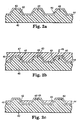
- the process of the present invention involves first providing a structured substrate 10 as shown in Fig. 1A .
- the substrate generally comprises a plurality of structural elements.
- the substrate 10 comprises a variety of arbitrarily-shaped protrusions 12 that rise above the main surface 14 of the substrate.
- the substrate 10 may be any material that is able to retain the imparted structure.
- the structure on the substrate may be of any arbitrary type such as posts, ribs, or other structures; they may be of any arbitrary shape; and they may be of any dimensions suitable for the specific application.
- the substrate comprises a microstructured surface such as is generated using known microreplication techniques, resulting in structures having characteristic dimensions on the order of 0.1 ⁇ m to on the order of 1000 ⁇ m.
- the substrate comprises a microstructured surface wherein the structures include a plurality of substantially parallel ridges.
- these ridges have heights of from about 0.1 ⁇ m to about 100 ⁇ m, widths of from about 0.5 ⁇ m to about 1000 ⁇ m, and spacing between them of from about 1 ⁇ m to about 10 mm.
- the process of the present invention next involves coating the structured substrate with a filler material 20.
- the filler material 20 is coated to a thickness, h , sufficient to cover the structures to be modified.
- the step of coating the structured substrate with filler material to cover the structures of the substrates is referred to as "flood coating.”
- Flood coating may be performed using any known technique for coating, and suitable coating techniques will be obvious to one of ordinary skill once the filler material is chosen. For example, if the filler material is coated in the liquid form, the filler may be applied by gravure roll, doctor blade, knife edge, or other conventional methods.
- the surface of the filler material is planed using methods such as those described hereinafter.
- the filler material is planed to provide a substantially uniform surface so that uniform removal of the filler yields the same results across the areas of the substrate to be modified.
- the step of planing the filler material on a structured substrate having a.plurality of protrusions may result in a filler layer having a substantially uniform main surface 22 and features representing remnants of the structured protrusions rising to a level 24 above the main surface 22 as shown in Fig. 1A .
- the thickness of the planed filler layer can thus be defined as follows: h is the thickness of the filler between the main substrate surface 14 and the main filler surface 22, d is the thickness between the substrate protrusion tops 16 and the filler surface above the protrusions 24, and r is the distance between the filler main surface 22 and the filler surface above the protrusions 24. It is desirable to minimize the ratio r / h in order to obtain a substantially uniform surface.
- the ratio r / h is preferably less than about 0.1, more preferably less than about 0.05, and most preferably less than about 0.01.
- the ratio d / h is preferably less than about 1.0, more preferably less than about 0.5, even more preferably less than about 0.2, and most preferably less than about 0.1.
- the step of planing the filler surface may be accomplished using any technique suitable for forming a uniform surface on the filler coating. For example, excess filler may be removed using a substantially flat blade scraped evenly across the surface with a uniform force. More than one pass with the blade may be required in order to achieve the desired degree of surface uniformity and in order to minimize the ratios r / h and d / h .
- Another method involves placing a release liner over the filler-coated substrate, moving a thin, flexible stainless steel sheet across the surface of the liner while applying a moderate force to smooth the filler material, curing the filler coating if necessary, and removing the liner.
- Yet another method involves partially immersing a coating roll in a pan of a filler material and advancing the substrate film over the coating roll with the structured side of the film contacting the coating roll.
- the thickness of the coating may be controlled by adjusting the tension of the substrate film against the coating roll. Multiple passes may be necessary.
- a similar method involves spreading a filler material on a structured substrate film and using a nip roll to press the substrate film and filler coating against a smooth embossing roll.
- the thickness of the filler coating may be controlled by adjusting the pressure between the nip roll and the smooth embossing drum.
- Other methods of planing the filler surface will be apparent to one of ordinary skill, and the suitability of a particular method of planing will be apparent given the choice of filler material.
- the steps of coating and planing will result in a structured substrate with a filler coating analogous to that shown in Fig. 1A , preferably with the ratios r / h and d / h minimize
- the process of the present invention continues by uniformly removing the filler material until those areas of the substrate structures to be modified are exposed, as shown in Fig. 1B .
- the filler coating may need to be hardened for the step of uniform removal. Suitable removal methods will depend on the choice of filler material as described hereinafter.
- the amount of filler material to be removed will depend on both the amount of substrate structure to be exposed and on the thickness d of the filler coating above the substrate structures. Therefore, in order to minimize both the filler removal time and the possibility of removing too much filler due to extended removal times, the thickness d should preferably be minimized.
- d is preferably on the order of or less than the height of the structures above the substrate main surface. More preferably, d is much less than the height of the structures above the substrate main surface.
- the filler material may be any material that can be coated onto the structured substrate to substantially cover the structures of the substrate, that can be planed to form a substantially uniform surface, and that can be preferentially and uniformly removed using a technique that does not substantially modify the substrate or the structures thereon.
- the filler material is a material that can be coated onto the structured substrate in the liquid form and then cured to provide a surface that may be planed concurrently or thereafter.
- the filler material is a material that can be removed using an etching process that does not adversely affect the structured substrate.
- the filler material is a photosensitive resist material as may be employed in conventional lithography. Such materials are preferred because they are easily handled and because techniques for their preferential removal are well known.
- Examples of specific filler materials and correspondingly suitable removal methods are as follows: (1) a photoresist sold under the trade designation Shipley Resist 1400-37 by Shipley Co., Marlborough, MA can be used as a filler and can be etched by exposure to collimated light from a Hg lamp with an intensity of 4.7 mW/cm 2 at a wavelength of 365 nm, immersion in a developer sold under the trade designation Shipley Developer 354 also by Shipley followed by rinsing, and baking at 120 degrees C; (2) a resist sold under the trade designation Ronascreen 2400 by LeaRonal, Freeport, NY can be used as a filler and can be etched by immersion in a 0.5% Na 2 CO 3 solution; (3) a resist comprising the mixture of isobomyl acrylate as sold by Radcure/UCB Chemicals Corporation, Smyrna, Georgia, with 12% by weight of a photoinitiator sold under the trade designation Darocure 1173 also by Radcure can be used as a
- filler materials or mixtures may be chosen depending upon the factors of cost, ease of use, compatibility with the substrate material, compatibility of suitable removal techniques with the substrate material, and the ability of the filler material to act as a resist to protect the areas of the substrate not to be modified from the applicable modification techniques.
- the step of planing the filler coating and the step of removing the filler coating until the areas to be modified are exposed may be modified by choosing filler materials having uniquely desirable properties or by mixing additives into filler materials to create desirable properties.
- the step of planing the surface of the filler coating can occur simultaneously with the step of coating the substrate with the filler material.
- the step of flood coating itself may result in a planed surface.
- Viscosity modifiers may be in the form of solvents or reactive dilutents that decrease the viscosity of the filler material when added, or thickening agents such as fumed silica that increase the viscosity of the filler material when added.
- the mixtures comprised amounts of the following materials: (a) a material sold under the trade designation SR340 by Sartomer Company, Exton, PA, (b) a material sold under the trade designation Photomer 6173 by Henkel Corp., Ambler, PA, (c) a photoinitiator sold under the trade designation CGI1700 by Ciba-Geigy Corporation, Tarrytown, NY, (d) iso octyl thio glycolate (IOTG), and (e) a surfactant sold under the trade designation FC430 by 3M Company, St. Paul, MN.
- Sample A was made by mixing 49.5 g of (a), 60.5 g of (b), 5.5 g of (c), 5.4 g of (d) and 0.33 g of (e), resulting in a filler material having a surface tension of 29.0 dynes/cm.
- Sample B was made by mixing 49.5 g of (a), 60.5 g of (b), 5.5 g of (c), 5.4 g of (d) and 0.083 g of (e), resulting in a filler material having a surface tension of 32.5 dynes/cm.
- Each filler material was coated on a substrate having a series of ridges that were approximately 4 ⁇ m high, 30 ⁇ m wide, and spaced 300 ⁇ m apart.
- Sample A yielded a coating having a thickness r (defined in Fig. 1A ) of 0.6 ⁇ m.
- Sample B yielded a coating having a planar surface with no measureable r thickness.
- the planing step may occur merely by applying the filler coating if the formulation of the resist material is correct.
- the filler material may also be formulated to have a surface tension that closely matches the surface energy of the surface of the substrate to be coated. This may yield desirable results when the filler material is coated to a thickness h that approximates the height of the protrusions on the substrate.
- the thickness of the filler coating closely matches, or is slightly less than, the height of the protrusions, and the surface tension of the filler material closely matches the free surface energy of the substrate, the tendency of the liquid filler material to dewet from the tops of the protrusions is maximized, thus leaving the tops of the protrusions substantially free of liquid filler material. If such conditions are reached, then the filler material need only be hardened to expose the tops of the protrusions to be modified. This special situation eliminates both the planing step and the step of removing filler material to expose the tops of the protrusions.
- the exposed portions is modified.
- the protrusion tops 16 have been fully exposed by uniform removal of a certain amount of the filler material 20.
- those portions of the substrate that are not to be modified remain protected by the filler material.
- the exposed areas can be modified by methods that include etching (or otherwise removing pre-existing external layers from the substrate protrusions) and depositing (or otherwise coating extra layers onto the exposed areas of the substrate).
- an additional amount of filler material is removed and is the substrate structures are further modified over a now larger area. In such a way, the steps of uniformly removing the filler and modifying the exposed areas of the substrate may be repeated to produce the desired substrate patterning.
- the remaining filler may be removed from the substrate by etching methods or simply by a lift-off method.
- the process of the present invention may be employed to pattern structured plastic substrates for liquid crystal displays with opaque, conductive coatings on the rib tops to serve both as a dark matrix and as conductive bus lines.
- liquid crystal display substrates having microstructured parallel ribs imparted thereto can be formed.
- the function of the ribs is to provide precision spacing elements that create a uniform gap between the main surface of the first, structured substrate and a second substrate in order to achieve a uniform display appearance even across large displays.
- Typical liquid crystal displays comprise two parallel substrates that confine a liquid crystal mixture in the uniform gap therebetween.
- twisted nematic liquid crystal devices for example, cholesteric liquid crystals are employed, the molecules of which have a helical or twisted molecular orientation.
- the molecules are oriented in the gap between the substrates so that each molecule goes through a 90 degree twist.
- the inside surface of each substrate includes parallel strips of a TCO, usually indium tin oxide, that act as independently addressable electrodes.
- the TCO strips of the first substrate are oriented perpendicular to the TCO strips of the second substrate so that the area through the display in which electrodes of the two substrates cross create picture elements (pixels).
- the ribs act as spacers between the two substrates and can also be used to physically separate the TCO strips for electrical isolation.
- the process of the present invention can be employed to pattern these TCO strips on the microstructured substrate.
- TCO materials have a relatively low conductivity, there may be noticeable delays in the response time of the display, especially when fast refresh rates are required and when large, high resolution displays are used.
- the process of the present invention can also be employed to pattern auxiliary conductive strips that will increase the conductivity of the TCO electrodes to thereby decrease the response time of the display.
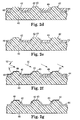
- a microstructured substrate 40 as depicted in Fig. 2(a) comprising parallel ribs 42 having dimensions 4.5 ⁇ m high, 30 ⁇ m wide, and spaced 300 ⁇ m apart (center to center), was coated with a 700 Angstrom thick film 44 of indium tin oxide (ITO), a common TCO material used in liquid crystal displays.
- ITO indium tin oxide
- the steps of patterning this substrate using one embodiment of the process of the present invention are depicted in Fig. 2(a)-(g) .
- the substrate was flood coated with a filler material 46 comprising Shipley Resist 1400-37 (as identified above), and the resist coating was planarized by scraping with a blade to form a uniform surface 47.
- the resulting resist coating thickness 45 above the rib tops 43 after the planing step was about 0.4 ⁇ m (shown in Fig. 2(b) ).
- the sample was then immersed in 0.1 % Na 2 CO 3 solution for 40 seconds to remove enough resist to expose the ITO coated rib tops 43 (shown in Fig. 2(c) ).
- the ITO layer 44 was etched from the rib tops 43 by immersing the sample in a 10% solution of HCl for 70 seconds at room temperature.
- This step created electrically isolated strips of ITO whereby the ITO remained in the valleys between ribs 42 and on the rib slopes 49 but not on the rib tops 43 (shown in Fig. 2(d) ). If the remaining photoresist were removed at this point, the resulting substrate would comprise suitably patterned ITO electrode strips for use in a liquid crystal display.
- the sample was next immersed in 0.1 % Na 2 CO 3 solution for another 40 seconds to remove more of the resist coating 46 and to thereby expose a portion of the ITO coated rib slopes 49, but without exposing the main surface of the substrate 40 (shown in Fig. 2(e) ).
- the sample was then coated with a 2000 Angstrom thick layer 48 of Cr metal by vacuum deposition.
- the Cr was deposited using a substantially collimated beam 50 incident upon the sample at an angle 52 which measured 15 degrees from a line in the plane of the substrate 40 perpendicular to the ribs 42 (shown in Fig. 2(f) ).
- each protrusion blocks the collimated beam from depositing material in an areas behind the protrusion, thus casting a "shadow.”
- shadow coating only the rib tops and the sides of the rib slopes facing the collimated deposition beam were coated with Cr, leaving a portion of the "back" side of the rib slopes free of both Cr and ITO (shown in Fig. 2(f) ). Thus, electrical isolation of the ITO strips was maintained.
- the remaining filler material was removed by lift-off (shown in Fig. 2(g) ).
- the Cr layer increases the conductivity of the ITO layer which it contacts.
- the conductivity of the ITO strips was increased by a factor of about 100.
- the amount by which the conductivity is increased can be adjusted higher or lower by depositing thicker or thinner metal layers.
- the transparency of the display substrate was not adversely affected because the opaque Cr layer was confined to the inactive regions of the device, namely the rib tops and a portion of the rib slopes. Only the flat areas of the substrate between the ribs are active areas.
- the opaque quality of the Cr layer performs a contrast-enhancing function in displays that do not employ a crossed polarizer construction.
- light in the inactive regions i.e. the rib tops where there is no liquid crystal
- the pixels When pixels are activated, they appear dark. If the inactive regions adjacent to activated pixels transmit light, the pixels appear gray rather than black, thus reducing, or "washing out," the contrast of the display.
- the rib tops do not allow light to be transmitted in the inactive regions. In this way, activated pixel areas appear black at the cost of adding thin dark lines that do not adversely affect the appearance of the lighted portions of the display.
Landscapes
- Physics & Mathematics (AREA)
- General Physics & Mathematics (AREA)
- Chemical & Material Sciences (AREA)
- Nonlinear Science (AREA)
- Engineering & Computer Science (AREA)
- Mathematical Physics (AREA)
- Crystallography & Structural Chemistry (AREA)
- Optics & Photonics (AREA)
- Architecture (AREA)
- Structural Engineering (AREA)
- Spectroscopy & Molecular Physics (AREA)
- General Chemical & Material Sciences (AREA)
- Chemical Kinetics & Catalysis (AREA)
- Materials Engineering (AREA)
- Mechanical Engineering (AREA)
- Metallurgy (AREA)
- Organic Chemistry (AREA)
- Application Of Or Painting With Fluid Materials (AREA)
- Liquid Crystal (AREA)
- Devices For Indicating Variable Information By Combining Individual Elements (AREA)
Applications Claiming Priority (3)
| Application Number | Priority Date | Filing Date | Title |
|---|---|---|---|
| US08/999,287 US6077560A (en) | 1997-12-29 | 1997-12-29 | Method for continuous and maskless patterning of structured substrates |
| US999287 | 1997-12-29 | ||
| PCT/US1998/008995 WO1999034256A1 (en) | 1997-12-29 | 1998-05-04 | Method for continuous and maskless patterning of structured substrates |
Publications (2)
| Publication Number | Publication Date |
|---|---|
| EP1044396A1 EP1044396A1 (en) | 2000-10-18 |
| EP1044396B1 true EP1044396B1 (en) | 2010-06-30 |
Family
ID=25546145
Family Applications (1)
| Application Number | Title | Priority Date | Filing Date |
|---|---|---|---|
| EP98920179A Expired - Lifetime EP1044396B1 (en) | 1997-12-29 | 1998-05-04 | Method for continuous and maskless patterning of structured substrates |
Country Status (7)
| Country | Link |
|---|---|
| US (1) | US6077560A (enExample) |
| EP (1) | EP1044396B1 (enExample) |
| JP (1) | JP2002500434A (enExample) |
| KR (1) | KR100567635B1 (enExample) |
| CA (1) | CA2315026A1 (enExample) |
| DE (1) | DE69841752D1 (enExample) |
| WO (1) | WO1999034256A1 (enExample) |
Families Citing this family (16)
| Publication number | Priority date | Publication date | Assignee | Title |
|---|---|---|---|---|
| US6524675B1 (en) | 1999-05-13 | 2003-02-25 | 3M Innovative Properties Company | Adhesive-back articles |
| KR20010082831A (ko) * | 2000-02-21 | 2001-08-31 | 구본준, 론 위라하디락사 | 액정표시장치의 제조방법 |
| WO2002092242A1 (en) * | 2001-05-16 | 2002-11-21 | Board Of Regents | Selective deposition of materials for the fabrication of interconnects and contacts on semiconductors devices |
| US20040067341A1 (en) * | 2002-10-02 | 2004-04-08 | Shartle Robert Justice | Scratch-resistant metal films and metallized surfaces and methods of fabricating them |
| JP3801158B2 (ja) * | 2002-11-19 | 2006-07-26 | セイコーエプソン株式会社 | 多層配線基板の製造方法、多層配線基板、電子デバイス及び電子機器 |
| TW594423B (en) * | 2003-08-28 | 2004-06-21 | Ind Tech Res Inst | A color filter manufacturing method for a plastic substrate |
| US7012017B2 (en) * | 2004-01-29 | 2006-03-14 | 3M Innovative Properties Company | Partially etched dielectric film with conductive features |
| US7528075B2 (en) * | 2004-02-25 | 2009-05-05 | Hrl Laboratories, Llc | Self-masking defect removing method |
| EP1840657A1 (en) * | 2006-03-28 | 2007-10-03 | Carl Zeiss SMT AG | Support structure for temporarily supporting a substrate |
| US7543974B2 (en) | 2007-03-06 | 2009-06-09 | Skc Haas Display Films Co., Ltd. | Light redirecting film having variable thickness |
| US7530726B2 (en) | 2007-03-06 | 2009-05-12 | Skc Haas Display Films Co., Ltd. | Light redirecting film having discontinuous coating |
| WO2009108334A2 (en) * | 2008-02-28 | 2009-09-03 | New York University | Method and apparatus for providing input to a processor, and a sensor pad |
| US8957484B2 (en) * | 2008-02-29 | 2015-02-17 | University Of Washington | Piezoelectric substrate, fabrication and related methods |
| WO2010002679A2 (en) * | 2008-06-30 | 2010-01-07 | 3M Innovative Properties Company | Method of forming a microstructure |
| JP5319769B2 (ja) * | 2008-06-30 | 2013-10-16 | スリーエム イノベイティブ プロパティズ カンパニー | パターン形成された基板の形成方法 |
| CN103547702B (zh) | 2010-06-04 | 2016-08-10 | 阿德文泰克全球有限公司 | 利用编码孔径进行的阴影掩模的对准 |
Family Cites Families (14)
| Publication number | Priority date | Publication date | Assignee | Title |
|---|---|---|---|---|
| US1983720A (en) * | 1934-01-26 | 1934-12-11 | Pittsburgh Plate Glass Co | Ornamental glass and method of making the same |
| US3244556A (en) * | 1962-10-01 | 1966-04-05 | Xerox Corp | Abrasion for thin film resistance control |
| US3287161A (en) * | 1962-10-01 | 1966-11-22 | Xerox Corp | Method for forming a thin film resistor |
| JPS6489470A (en) * | 1987-09-30 | 1989-04-03 | Mitsubishi Electric Corp | Manufacture of semiconductor device |
| DE3888184D1 (de) * | 1988-11-17 | 1994-04-07 | Ibm | Verfahren zur Herstellung von Masken mit Strukturen im Submikrometerbereich. |
| US5156986A (en) * | 1990-10-05 | 1992-10-20 | General Electric Company | Positive control of the source/drain-gate overlap in self-aligned TFTS via a top hat gate electrode configuration |
| JP3173803B2 (ja) * | 1990-12-10 | 2001-06-04 | キヤノン株式会社 | 回折格子の作成方法 |
| US5538753A (en) * | 1991-10-14 | 1996-07-23 | Landis & Gyr Betriebs Ag | Security element |
| KR960003864B1 (ko) * | 1992-01-06 | 1996-03-23 | 삼성전자주식회사 | 반도체 메모리장치 및 그 제조방법 |
| US5268782A (en) * | 1992-01-16 | 1993-12-07 | Minnesota Mining And Manufacturing Company | Micro-ridged, polymeric liquid crystal display substrate and display device |
| US5292625A (en) * | 1992-04-03 | 1994-03-08 | Minnesota Mining And Manufacturing Company | Method for selectively exposing an uneven substrate surface |
| US5378494A (en) * | 1994-02-18 | 1995-01-03 | Minnesota Mining And Manufacturing Company | Method of applying a thin coating on the lower surface of a bilevel substrate |
| US5382317A (en) * | 1994-02-18 | 1995-01-17 | Minnesota Mining And Manufacturing Company | Method of selectively applying a coating to a bilevel substrate |
| US5686337A (en) * | 1996-01-11 | 1997-11-11 | Vanguard International Semiconductor Corporation | Method for fabricating stacked capacitors in a DRAM cell |
-
1997
- 1997-12-29 US US08/999,287 patent/US6077560A/en not_active Expired - Lifetime
-
1998
- 1998-05-04 WO PCT/US1998/008995 patent/WO1999034256A1/en not_active Ceased
- 1998-05-04 KR KR1020007007213A patent/KR100567635B1/ko not_active Expired - Fee Related
- 1998-05-04 DE DE69841752T patent/DE69841752D1/de not_active Expired - Lifetime
- 1998-05-04 JP JP2000526846A patent/JP2002500434A/ja active Pending
- 1998-05-04 EP EP98920179A patent/EP1044396B1/en not_active Expired - Lifetime
- 1998-05-04 CA CA002315026A patent/CA2315026A1/en not_active Abandoned
Also Published As
| Publication number | Publication date |
|---|---|
| US6077560A (en) | 2000-06-20 |
| EP1044396A1 (en) | 2000-10-18 |
| KR100567635B1 (ko) | 2006-04-05 |
| WO1999034256A1 (en) | 1999-07-08 |
| CA2315026A1 (en) | 1999-07-08 |
| DE69841752D1 (de) | 2010-08-12 |
| JP2002500434A (ja) | 2002-01-08 |
| KR20010033690A (ko) | 2001-04-25 |
Similar Documents
| Publication | Publication Date | Title |
|---|---|---|
| EP1044396B1 (en) | Method for continuous and maskless patterning of structured substrates | |
| KR100831232B1 (ko) | 액정표시장치용 컬러필터 및 이를 이용한 액정표시장치 | |
| US5663019A (en) | Process for producing multicolor display | |
| US6855465B2 (en) | Color filter substrate and method for fabricating the same | |
| JP3670577B2 (ja) | 液晶表示装置およびその製造方法 | |
| US6068953A (en) | Color filter for liquid crystal display device | |
| JP3611618B2 (ja) | 非晶質導電膜のパターニング方法 | |
| JP2003149429A (ja) | 突起構造付きカラーフィルターの形成方法及び突起構造付きカラーフィルター | |
| KR100305443B1 (ko) | 표면에윈도우형및프레임형코팅막이형성된기판의제조방법 | |
| US20020031852A1 (en) | Method of fabricating a liquid crystal display | |
| JPH08292426A (ja) | 液晶表示装置およびその製造方法 | |
| JP2001330826A (ja) | 反射型lcdおよびその製造方法 | |
| US6455339B1 (en) | Method for fabricating protrusion of liquid crystal display | |
| CN114609816A (zh) | 显示面板及其制作方法 | |
| US8173225B2 (en) | Photocurable organic material and method of fabricating array substrate for liquid crystal display device using the same | |
| JPH0414021A (ja) | 液晶表示パネル及びその製造方法 | |
| JP3175954B2 (ja) | 液晶表示素子およびその製造方法 | |
| JP2000111726A (ja) | カラーフィルタおよびその製造方法 | |
| CN114690476B (zh) | 显示面板及其制作方法 | |
| JP3391876B2 (ja) | カラーフィルタの製造方法 | |
| CN1194366C (zh) | 等离子体显示板银电极制作方法 | |
| JPH0784115A (ja) | 機能性塗膜を形成する方法 | |
| KR100437596B1 (ko) | 컬러 필터 기판 제조방법 | |
| JP2001166286A (ja) | 光反射性基板の製造方法および液晶表示素子 | |
| JP2002040399A (ja) | 光反射性基板の製造方法および液晶表示素子 |
Legal Events
| Date | Code | Title | Description |
|---|---|---|---|
| PUAI | Public reference made under article 153(3) epc to a published international application that has entered the european phase |
Free format text: ORIGINAL CODE: 0009012 |
|
| 17P | Request for examination filed |
Effective date: 20000719 |
|
| AK | Designated contracting states |
Kind code of ref document: A1 Designated state(s): BE DE DK FR GB IT NL |
|
| 17Q | First examination report despatched |
Effective date: 20071114 |
|
| GRAP | Despatch of communication of intention to grant a patent |
Free format text: ORIGINAL CODE: EPIDOSNIGR1 |
|
| RIC1 | Information provided on ipc code assigned before grant |
Ipc: G02F 1/1343 20060101ALI20091102BHEP Ipc: G03F 7/00 20060101ALI20091102BHEP Ipc: G03F 7/09 20060101AFI20091102BHEP |
|
| GRAS | Grant fee paid |
Free format text: ORIGINAL CODE: EPIDOSNIGR3 |
|
| GRAA | (expected) grant |
Free format text: ORIGINAL CODE: 0009210 |
|
| AK | Designated contracting states |
Kind code of ref document: B1 Designated state(s): BE DE DK FR GB IT NL |
|
| REG | Reference to a national code |
Ref country code: GB Ref legal event code: FG4D |
|
| REF | Corresponds to: |
Ref document number: 69841752 Country of ref document: DE Date of ref document: 20100812 Kind code of ref document: P |
|
| REG | Reference to a national code |
Ref country code: NL Ref legal event code: VDEP Effective date: 20100630 |
|
| PG25 | Lapsed in a contracting state [announced via postgrant information from national office to epo] |
Ref country code: NL Free format text: LAPSE BECAUSE OF FAILURE TO SUBMIT A TRANSLATION OF THE DESCRIPTION OR TO PAY THE FEE WITHIN THE PRESCRIBED TIME-LIMIT Effective date: 20100630 |
|
| PG25 | Lapsed in a contracting state [announced via postgrant information from national office to epo] |
Ref country code: BE Free format text: LAPSE BECAUSE OF FAILURE TO SUBMIT A TRANSLATION OF THE DESCRIPTION OR TO PAY THE FEE WITHIN THE PRESCRIBED TIME-LIMIT Effective date: 20100630 |
|
| PG25 | Lapsed in a contracting state [announced via postgrant information from national office to epo] |
Ref country code: IT Free format text: LAPSE BECAUSE OF FAILURE TO SUBMIT A TRANSLATION OF THE DESCRIPTION OR TO PAY THE FEE WITHIN THE PRESCRIBED TIME-LIMIT Effective date: 20100630 |
|
| PG25 | Lapsed in a contracting state [announced via postgrant information from national office to epo] |
Ref country code: DK Free format text: LAPSE BECAUSE OF FAILURE TO SUBMIT A TRANSLATION OF THE DESCRIPTION OR TO PAY THE FEE WITHIN THE PRESCRIBED TIME-LIMIT Effective date: 20100630 |
|
| PLBE | No opposition filed within time limit |
Free format text: ORIGINAL CODE: 0009261 |
|
| STAA | Information on the status of an ep patent application or granted ep patent |
Free format text: STATUS: NO OPPOSITION FILED WITHIN TIME LIMIT |
|
| 26N | No opposition filed |
Effective date: 20110331 |
|
| REG | Reference to a national code |
Ref country code: DE Ref legal event code: R097 Ref document number: 69841752 Country of ref document: DE Effective date: 20110330 |
|
| GBPC | Gb: european patent ceased through non-payment of renewal fee |
Effective date: 20110504 |
|
| REG | Reference to a national code |
Ref country code: FR Ref legal event code: ST Effective date: 20120131 |
|
| REG | Reference to a national code |
Ref country code: DE Ref legal event code: R119 Ref document number: 69841752 Country of ref document: DE Effective date: 20111201 |
|
| PG25 | Lapsed in a contracting state [announced via postgrant information from national office to epo] |
Ref country code: FR Free format text: LAPSE BECAUSE OF NON-PAYMENT OF DUE FEES Effective date: 20110531 |
|
| PG25 | Lapsed in a contracting state [announced via postgrant information from national office to epo] |
Ref country code: GB Free format text: LAPSE BECAUSE OF NON-PAYMENT OF DUE FEES Effective date: 20110504 |
|
| PG25 | Lapsed in a contracting state [announced via postgrant information from national office to epo] |
Ref country code: DE Free format text: LAPSE BECAUSE OF NON-PAYMENT OF DUE FEES Effective date: 20111201 |