EP1031939B1 - Composite ic card - Google Patents
Composite ic card Download PDFInfo
- Publication number
- EP1031939B1 EP1031939B1 EP98953057A EP98953057A EP1031939B1 EP 1031939 B1 EP1031939 B1 EP 1031939B1 EP 98953057 A EP98953057 A EP 98953057A EP 98953057 A EP98953057 A EP 98953057A EP 1031939 B1 EP1031939 B1 EP 1031939B1
- Authority
- EP
- European Patent Office
- Prior art keywords
- card
- module
- coil
- antenna
- region
- Prior art date
- Legal status (The legal status is an assumption and is not a legal conclusion. Google has not performed a legal analysis and makes no representation as to the accuracy of the status listed.)
- Expired - Lifetime
Links
Images


Classifications
-
- G—PHYSICS
- G06—COMPUTING OR CALCULATING; COUNTING
- G06K—GRAPHICAL DATA READING; PRESENTATION OF DATA; RECORD CARRIERS; HANDLING RECORD CARRIERS
- G06K19/00—Record carriers for use with machines and with at least a part designed to carry digital markings
- G06K19/06—Record carriers for use with machines and with at least a part designed to carry digital markings characterised by the kind of the digital marking, e.g. shape, nature, code
-
- G—PHYSICS
- G06—COMPUTING OR CALCULATING; COUNTING
- G06K—GRAPHICAL DATA READING; PRESENTATION OF DATA; RECORD CARRIERS; HANDLING RECORD CARRIERS
- G06K7/00—Methods or arrangements for sensing record carriers, e.g. for reading patterns
- G06K7/10—Methods or arrangements for sensing record carriers, e.g. for reading patterns by electromagnetic radiation, e.g. optical sensing; by corpuscular radiation
- G06K7/10009—Methods or arrangements for sensing record carriers, e.g. for reading patterns by electromagnetic radiation, e.g. optical sensing; by corpuscular radiation sensing by radiation using wavelengths larger than 0.1 mm, e.g. radio-waves or microwaves
- G06K7/10158—Methods or arrangements for sensing record carriers, e.g. for reading patterns by electromagnetic radiation, e.g. optical sensing; by corpuscular radiation sensing by radiation using wavelengths larger than 0.1 mm, e.g. radio-waves or microwaves methods and means used by the interrogation device for reliably powering the wireless record carriers using an electromagnetic interrogation field
- G06K7/10178—Methods or arrangements for sensing record carriers, e.g. for reading patterns by electromagnetic radiation, e.g. optical sensing; by corpuscular radiation sensing by radiation using wavelengths larger than 0.1 mm, e.g. radio-waves or microwaves methods and means used by the interrogation device for reliably powering the wireless record carriers using an electromagnetic interrogation field including auxiliary means for focusing, repeating or boosting the electromagnetic interrogation field
-
- G—PHYSICS
- G06—COMPUTING OR CALCULATING; COUNTING
- G06K—GRAPHICAL DATA READING; PRESENTATION OF DATA; RECORD CARRIERS; HANDLING RECORD CARRIERS
- G06K19/00—Record carriers for use with machines and with at least a part designed to carry digital markings
- G06K19/06—Record carriers for use with machines and with at least a part designed to carry digital markings characterised by the kind of the digital marking, e.g. shape, nature, code
- G06K19/067—Record carriers with conductive marks, printed circuits or semiconductor circuit elements, e.g. credit or identity cards also with resonating or responding marks without active components
- G06K19/07—Record carriers with conductive marks, printed circuits or semiconductor circuit elements, e.g. credit or identity cards also with resonating or responding marks without active components with integrated circuit chips
- G06K19/077—Constructional details, e.g. mounting of circuits in the carrier
- G06K19/07745—Mounting details of integrated circuit chips
- G06K19/07747—Mounting details of integrated circuit chips at least one of the integrated circuit chips being mounted as a module
-
- G—PHYSICS
- G06—COMPUTING OR CALCULATING; COUNTING
- G06K—GRAPHICAL DATA READING; PRESENTATION OF DATA; RECORD CARRIERS; HANDLING RECORD CARRIERS
- G06K19/00—Record carriers for use with machines and with at least a part designed to carry digital markings
- G06K19/06—Record carriers for use with machines and with at least a part designed to carry digital markings characterised by the kind of the digital marking, e.g. shape, nature, code
- G06K19/067—Record carriers with conductive marks, printed circuits or semiconductor circuit elements, e.g. credit or identity cards also with resonating or responding marks without active components
- G06K19/07—Record carriers with conductive marks, printed circuits or semiconductor circuit elements, e.g. credit or identity cards also with resonating or responding marks without active components with integrated circuit chips
- G06K19/077—Constructional details, e.g. mounting of circuits in the carrier
- G06K19/07749—Constructional details, e.g. mounting of circuits in the carrier the record carrier being capable of non-contact communication, e.g. constructional details of the antenna of a non-contact smart card
- G06K19/0775—Constructional details, e.g. mounting of circuits in the carrier the record carrier being capable of non-contact communication, e.g. constructional details of the antenna of a non-contact smart card arrangements for connecting the integrated circuit to the antenna
- G06K19/07756—Constructional details, e.g. mounting of circuits in the carrier the record carrier being capable of non-contact communication, e.g. constructional details of the antenna of a non-contact smart card arrangements for connecting the integrated circuit to the antenna the connection being non-galvanic, e.g. capacitive
-
- G—PHYSICS
- G06—COMPUTING OR CALCULATING; COUNTING
- G06K—GRAPHICAL DATA READING; PRESENTATION OF DATA; RECORD CARRIERS; HANDLING RECORD CARRIERS
- G06K19/00—Record carriers for use with machines and with at least a part designed to carry digital markings
- G06K19/06—Record carriers for use with machines and with at least a part designed to carry digital markings characterised by the kind of the digital marking, e.g. shape, nature, code
- G06K19/067—Record carriers with conductive marks, printed circuits or semiconductor circuit elements, e.g. credit or identity cards also with resonating or responding marks without active components
- G06K19/07—Record carriers with conductive marks, printed circuits or semiconductor circuit elements, e.g. credit or identity cards also with resonating or responding marks without active components with integrated circuit chips
- G06K19/077—Constructional details, e.g. mounting of circuits in the carrier
- G06K19/07749—Constructional details, e.g. mounting of circuits in the carrier the record carrier being capable of non-contact communication, e.g. constructional details of the antenna of a non-contact smart card
- G06K19/07766—Constructional details, e.g. mounting of circuits in the carrier the record carrier being capable of non-contact communication, e.g. constructional details of the antenna of a non-contact smart card comprising at least a second communication arrangement in addition to a first non-contact communication arrangement
- G06K19/07769—Constructional details, e.g. mounting of circuits in the carrier the record carrier being capable of non-contact communication, e.g. constructional details of the antenna of a non-contact smart card comprising at least a second communication arrangement in addition to a first non-contact communication arrangement the further communication means being a galvanic interface, e.g. hybrid or mixed smart cards having a contact and a non-contact interface
-
- G—PHYSICS
- G06—COMPUTING OR CALCULATING; COUNTING
- G06K—GRAPHICAL DATA READING; PRESENTATION OF DATA; RECORD CARRIERS; HANDLING RECORD CARRIERS
- G06K19/00—Record carriers for use with machines and with at least a part designed to carry digital markings
- G06K19/06—Record carriers for use with machines and with at least a part designed to carry digital markings characterised by the kind of the digital marking, e.g. shape, nature, code
- G06K19/067—Record carriers with conductive marks, printed circuits or semiconductor circuit elements, e.g. credit or identity cards also with resonating or responding marks without active components
- G06K19/07—Record carriers with conductive marks, printed circuits or semiconductor circuit elements, e.g. credit or identity cards also with resonating or responding marks without active components with integrated circuit chips
- G06K19/077—Constructional details, e.g. mounting of circuits in the carrier
- G06K19/07749—Constructional details, e.g. mounting of circuits in the carrier the record carrier being capable of non-contact communication, e.g. constructional details of the antenna of a non-contact smart card
- G06K19/07773—Antenna details
- G06K19/07775—Antenna details the antenna being on-chip
-
- G—PHYSICS
- G06—COMPUTING OR CALCULATING; COUNTING
- G06K—GRAPHICAL DATA READING; PRESENTATION OF DATA; RECORD CARRIERS; HANDLING RECORD CARRIERS
- G06K19/00—Record carriers for use with machines and with at least a part designed to carry digital markings
- G06K19/06—Record carriers for use with machines and with at least a part designed to carry digital markings characterised by the kind of the digital marking, e.g. shape, nature, code
- G06K19/067—Record carriers with conductive marks, printed circuits or semiconductor circuit elements, e.g. credit or identity cards also with resonating or responding marks without active components
- G06K19/07—Record carriers with conductive marks, printed circuits or semiconductor circuit elements, e.g. credit or identity cards also with resonating or responding marks without active components with integrated circuit chips
- G06K19/077—Constructional details, e.g. mounting of circuits in the carrier
- G06K19/07749—Constructional details, e.g. mounting of circuits in the carrier the record carrier being capable of non-contact communication, e.g. constructional details of the antenna of a non-contact smart card
- G06K19/07773—Antenna details
- G06K19/07777—Antenna details the antenna being of the inductive type
- G06K19/07779—Antenna details the antenna being of the inductive type the inductive antenna being a coil
- G06K19/07783—Antenna details the antenna being of the inductive type the inductive antenna being a coil the coil being planar
-
- G—PHYSICS
- G06—COMPUTING OR CALCULATING; COUNTING
- G06K—GRAPHICAL DATA READING; PRESENTATION OF DATA; RECORD CARRIERS; HANDLING RECORD CARRIERS
- G06K19/00—Record carriers for use with machines and with at least a part designed to carry digital markings
- G06K19/06—Record carriers for use with machines and with at least a part designed to carry digital markings characterised by the kind of the digital marking, e.g. shape, nature, code
- G06K19/067—Record carriers with conductive marks, printed circuits or semiconductor circuit elements, e.g. credit or identity cards also with resonating or responding marks without active components
- G06K19/07—Record carriers with conductive marks, printed circuits or semiconductor circuit elements, e.g. credit or identity cards also with resonating or responding marks without active components with integrated circuit chips
- G06K19/077—Constructional details, e.g. mounting of circuits in the carrier
- G06K19/07749—Constructional details, e.g. mounting of circuits in the carrier the record carrier being capable of non-contact communication, e.g. constructional details of the antenna of a non-contact smart card
- G06K19/07773—Antenna details
- G06K19/07777—Antenna details the antenna being of the inductive type
- G06K19/07784—Antenna details the antenna being of the inductive type the inductive antenna consisting of a plurality of coils stacked on top of one another
Definitions
- the present invention relates to a smart card having both a function of a contact type in which reception of supply power, transmission/reception of signals, etc. are performed via an electrical contact, and a function of a non-contact type in which reception of supply power, transmission/reception of signals, etc. are performed without provision of an electrical contact, in an information recording medium represented by IC cards, etc. used in fields such as office automation (OA), factory automation (FA) or security.
- OA office automation
- FA factory automation
- IC cards are internationally standardized by the ISO (International Organization for Standardization).
- an IC such as a semiconductor memory is built in a card body formed of a plastic material as a basic material and metallic conductive terminal electrodes are provided on a card surface for connection with an external read/write apparatus.
- the IC card is inserted in a card slot of the external read/write apparatus and the terminal electrodes of the IC card are connected to the external read/write apparatus.
- This is suitable for uses requiring security and safety for communication as in large-volume data exchange and banking processing, for example, uses for crediting and electronic wallets.
- Radio Frequency Identification RFID
- a hard logic which does not have a battery cell and a CPU (Central Processing Unit).
- RFID Radio Frequency Identification
- CPU Central Processing Unit
- a metallic foil antenna coil for non-contact transmission which is formed by etching, is sandwiched between a sheet with engagement hole for an IC module and a substrate.
- the structure is laminated to produce a card body.
- two antenna terminals for connection between the antenna coil and the IC module are exposed to an inside of the engagement hole in the card body.
- This mounting method is relatively simple. However, it is difficult to confirm the state of the connection portion between the IC module and antenna, and a problem remains with the reliability of connection. In addition, degradation in the connection portion may easily occur due to mechanical stress. Moreover, since a step for applying the conductive adhesive and a thermocompression step are required for the connection between the IC module and antenna, it is difficult to use an apparatus for manufacturing a conventional IC card with external terminals. It is thus necessary to provide a new manufacturing line.
- an emboss or a magnetic stripe cannot be applied due to restrictions of the coil shape, etc. for keeping reception power.
- the emboss and magnetic stripe have to be considered. Techniques which do not permit provision of an emboss or a magnetic stripe are restricted in the range of application.
- a non-contact-type IC card disclosed, for example, in Jpn. Pat. Appln. KOKAI Publication No. 8-227,447 permits provision of an emboss and a magnetic stripe.
- a non-contact-type IC card having an outer shape according to ISO 7811 is provided.
- a communication IC module is constructed such that an IC mount portion, a power receiving coil and a data transmission/reception coil are arranged in a longitudinal direction on a region excluding the magnetic stripe region and embossing region.
- the reception coil and communication coil of the communication IC module are comprised of single-layer coils formed by electrocasting. Both are buried in a single strip-like substrate. Lead portions for connection with pads of the IC chip are formed of each coil.
- the IC chip is mounted on the strip-like substrate such that a circuit surface of the IC chip is opposed to the strip-like substrate.
- the lead portions are bump-bonded to the IC pads and a gap between the strip-like substrate and IC chip is filled with a potting resin for fixation.
- An inner end portion of the coil and an end portion of an internal-end lead are jumper-bonded by an enamel copper wire. The bonding is effected by instantaneous thermocompression and terminal portions are protected with potting resin.
- a method of integrating this communication IC module and the card is described. According to this method, there are provided a first sheet for covering the upper surface, a second sheet having the same thickness as the strip-like substrate and having a window with a strip-like outer shape, a third sheet having a window for passing the IC chip and a window for passing a first jumper-bonding portion, a fourth sheet having only a window for passing the IC chip, and a fifth sheet for covering the lower surface (all formed of vinyl chloride).
- the communication module is sandwiched by the respective sheets and subjected to thermocompression. Thus, the communication module is integrated in the card.
- FIG. 1 shows a magnetic stripe region, an embossing region and an external terminal region specified by ISO 7816.
- an IC module is mounted on the external terminal region.
- FIG. 1 in the regions indicated by hatching, mounting of an antenna for non-contact coupling is prohibited.
- ISO 7816 specifies an outer long side to be 85.47-85.72 mm, an outer short side to be 53.29-54.03 mm.
- the magnetic stripe region is defined in an area of 15.82 mm from the upper side.
- the embossing region is defined in an area of 24 mm from the lower side, 6.0 mm from the left side, and 8.0 mm from the right side.
- the external terminals are formed in an area of 28.55 mm from the upper side and 19.87 mm from the left side.
- Jpn. Pat. Appln. KOKAI Publication No. 7-239,922 discloses a prior-art technique of a smart card realizing a magnetic stripe and embossing.
- the IC module for the IC card comprises an IC chip; a transmission mechanism connected to the IC chip for effecting transmission of information and/or power with the external apparatus; and a support member for supporting the IC chip and transmission mechanism.
- the transmission mechanism comprises a non-contact-type transmission mechanism having a coil or an antenna, and a contact-type transmission mechanism having a plurality of terminal electrodes of patterned conductors provided on a surface of the support member.
- the document further discloses, as mounting means, that the antenna or coil for non-contact transmission is provided so as to surround the terminal electrodes, and alternatively the antenna is positioned at the center and the terminal electrodes are provided around the antenna.
- the non-contact transmission antenna is contained in the IC module and thereby the connection between the antenna coil and the IC module is omitted in the final step.
- the antenna or coil Since the distance between the terminal electrodes and embossing region is 1.45 mm at maximum, it is not practical to dispose the antenna or coil so as to surround the terminal electrodes without overlapping the terminal electrodes, as will be described below. In the case where the antenna coil is disposed around the external terminals, the maximum outside diameter and minimum inside diameter of the coil are ⁇ 12 mm and ⁇ 9.3 mm, respectively. If the antenna coil is formed of a print pattern in this region, where the pattern width and interval are 0.15 mm and 0.1 mm respectively, the number of turns and the inductance become about four and 0.4 ⁇ H, and six and 1.0 ⁇ H in respective cases ( ⁇ H denotes microhenry).
- the merit of adding the non-contact transmission function is small.
- the merit of adding the non-contact transmission mechanism to the contact type transmission mechanism is obtained with a communication distance exceeding several-ten mm to 100 mm. Communication is achieved if the card is exposed to the antenna unit of the external read/write apparatus within such an area. For this purpose, it is necessary to increase the area of the coil or the number of turns.
- the coil is disposed around the outer periphery of the terminal electrodes within the IC module, only several turns are obtained even if the print coil is formed, and owing to the smallness of the area of the coil, too, adequate power cannot be obtained. Moreover, if a practical number of turns is to be obtained with a conductor pattern, it overlaps the embossing region.
- FIG. 2 shows an equivalent circuit of a non-contact coupler circuit for describing the principle of the non-contact transmission mechanism.
- a transmission/reception circuit 101 of a non-contact type external read/write apparatus 100 is connected to a transmission/reception coil 102 which is an electromagnetic coupler for supplying power to, and exchanging information with, the non-contact transmission mechanism in the smart card.
- the non-contact transmission mechanism of the smart card 1 comprises an antenna coil 4, connected electromagnetically and directly to the transmission/reception antenna 102 of the external read/write apparatus 100, for receiving power and exchanging information; a capacitive element 15 connected between both ends of the antenna coil 4 to constitute a parallel resonance circuit; an IC chip 6 mounted on an IC module 2; a first coupler coil 8 connected to the IC chip 6; and a second coupler coil 3 closely coupled and disposed to transmit a signal received by the antenna coil 4 to the first coupler coil 8 with a maximum efficiency and connected between both ends of the capacitive element 15 of the parallel resonance circuit.
- the capacitive element 15 is connected in parallel to the antenna coil 4, it may preferably be connected in series between the antenna coil 4 and second coupler coil 3. If the parasitic capacity is increased, the capacitive element 15 can be dispensed with.
- a current is caused to flow in the parallel resonance circuit, which comprises the antenna coil 4 and capacitive element 15 of the smart card 1, due to the high-frequency magnetic field produced by the transmission/reception coil 102 of the external read/write apparatus 100.
- currents due to the high-frequency magnetic field are also induced in the first coupler coil 8 connected directly to the IC chip 6 and the second coupler coil 3 connected to the resonance circuit of the antenna coil 4 and capacitive element 15 to transmit power to the first coupler coil 8.
- the amount of induced currents in this case is less than that of current induced in the antenna coil 4 by an order of magnitude, and accordingly the sensitivity of reception depends greatly on characteristics of the antenna coil 4.
- a signal received by the resonance circuit of the antenna coil 4 and capacitive element 15 is transmitted to the second coupler coil 3. Since the second coupler coil 3 and first coupler coil 8 are closely coupled and disposed with a maximum transmission efficiency, the signal is then transmitted to the IC chip 6 via transformer coupling of the second coupler coil 3 and first coupler coil 8. The maximum transmission efficiency of transformer coupling between the second coupler coil 3 and first coupler coil 8 is determined by selection of the circuit constant.
- the antenna characteristics vary depending on the method of the non-contact transmission mechanism, such as electromagnetic coupling, electromagnetic induction, etc..
- the antenna coil characteristics with the electromagnetic induction method in a short-wave band are calculated, for example, as shown in TABLE 1.
- the thickness and pitch of the coil are 0.05 mm in the case of *1 alone. In the other cases, the thickness and pitch of the coil are 0.15 mm.
- the inductance of the antenna coil of the currently used RF-ID card for the short-wave band is about 5 microhenries.
- This type of antenna coil can be disposed on an outer peripheral portion of the card by means of a print pattern (print coil).
- Coils having more than eight turns can be realized by a spiral coil of a three-dimensional shape and a planer print coil.
- the spiral coil it is wound in an overlapping manner and thus can be disposed at an outer peripheral portion of the card.
- the print coil it is generally formed in a non-overlapping manner. Accordingly, where the number of turns is large, it is not proper to dispose the coil at the outer peripheral portion of the card so as to avoid overlapping with the embossing region.
- the card can be fabricated at low cost with simple manufacturing process and with high reliability.
- FIG. 3A and FIG. 3B show a schematic structure of a smart card according to a first arrangement.
- FIG. 3A shows the whole structure and
- FIG. 3B shows a cross-sectional structure of the mounting portion of the IC module.
- the smart card 1 according to the present arrangement is fabricated in a manner described below.
- the antenna substrate 5 is sealed by injection molding to form the card substrate 10.
- the second coupler coil 3 is positioned to overlap the mounting position of the IC module 2.
- an engagement hole 11 for the IC module 2 is formed.
- the card substrate is formed of vinyl chloride, but other materials such as polycarbonate are applicable to the present invention if characteristics of the card such as adequate strength and embossing processability are obtained.
- the card substrate 10 is shown as being divided into an obverse side portion and a reverse side portion. However, the card substrate 10 is actually a single piece. In the figure, the card substrate is shown in a modified fashion in order to clearly describe a relationship between the coupler coil and engagement hole 11 of the antenna substrate 5 which is sealed in the card substrate.
- the card is fabricated by injection molding. Any method, however, is applicable if characteristics of embossing are maintained. For instance, a laminating method or an adhesive filling method may be adopted.
- the engagement hole 11 for the IC module is made by cutting after the fabrication of the card.
- FIG. 4 is a plan view of the first arrangement of the smart card having an embossing region, showing a position of mounting of the antenna coil 4 within the smart card 1.
- the antenna coil 4 is disposed over the entire peripheral portion of the card.
- the embossing region 20 and external terminal region 21 are disposed within the loop of the antenna coil 4.
- the specifications of this coil correspond to example 1 in TABLE 1.
- FIG. 4 is effective where the number of turns of antenna coil 4 is relatively small, specifically, 3 to 7, and preferably 4 or 5.
- the antenna substrate 5 in this example of mounting that portion of the resin sheet, which corresponds to the embossing region 20, is cut out. This aims at preventing an adverse effect on embossing characteristics.
- FIGS. 4 to 7 the outer contours of the antenna substrates 5 are indicated by broken lines.
- FIG. 5 is a plan view of another smart card 1 according to a first embodiment of the invention having the embossing region.
- This figure shows a general shape of the antenna coil 4, on the outside of which the embossing region 20 and external terminal region 21 are disposed (i.e. not within the antenna coil).
- the specifications of this coil correspond to example 3 in TABLE 1.
- the example of FIG. 5 is effective where the number of turns of the antenna coil 4 is 10 or more.
- FIG. 6 is a plan view of a third example of mounting of the smart card 1 according to the first arrangement, which has both the magnetic stripe and embossing region.
- This figure shows a position of mounting of the antenna coil 4 in the smart card 1.
- the antenna coil 4 is made not to overlap the magnetic stripe region 22. That portion of the antenna coil, which excludes a portion thereof opposed to the magnetic stripe region, is disposed along the outer periphery of the smart card 1.
- the specifications of this coil correspond to example 2 in TABLE 1.
- the antenna substrate 5 in this example of mounting too, that portion of the resin sheet, which corresponds to the embossing region 20, is cut out. This aims at preventing an adverse effect on embossing characteristics.
- FIG. 7 is a plan view of a fourth example of mounting of the smart card 1 according to the first embodiment of the invention, which has both the magnetic stripe and embossing region.
- This figure shows a general shape of the antenna coil 4 which is disposed not to include the embossing region 20 or magnetic stripe region 22.
- the specifications of this coil correspond to example 4 in TABLE 1.
- the smart card according to the first arrangement has functions compatible with both the contact-type system with external terminals and the non-contact-type system with non-contact coupling elements such as an antenna coil.
- non-contact coupling elements such as an antenna coil.
- the area of the antenna coil is increased to a maximum permissible level.
- the reception sensitivity of the card is enhanced, the communication distance is increased and/or the transmission output of the external read/write apparatus can be reduced. This is convenient for cards since the transmission output is restricted by the Wireless Conducty Act.
- the antenna coil which is directly brought into non-contact coupling with the external read/write apparatus is so disposed as not to overlap the external terminal region of the non-contact-type electrodes, which is also the IC module engagement region, the embossing region and/or the magnetic stripe region, this invention permits general-purpose applications and is fully applicable to conventional cards.
- the thickness of the card can be set to fully meet the standard of ISO 7816, i.e. 0.76 mm.
- the increase in the number of turns of the first coupler coil 8 increases a coefficient of coupling with the second coupler coil 3, and energy to be transmitted to the IC chip 6 further increases.
- the limit pattern width is 0.1 mm. It is difficult to form several-ten turns of a print coil in the module substrate of the IC card.
- a coil is formed of an insulation-coated conductor wire, a diameter of several-ten microns is attained by virtue of development in magnetic head technology.
- the coupler coils for the IC module and antenna may be formed of an insulation-coated conductor wire.
- a smart card wherein no connection is required between the IC module and non-contact transmission antenna coil, a reception sensitivity capable of obtaining an adequate communication distance is attained, the IC card is compatible with both embossing processing and magnetic stripe formation, and both a contact-type and a non-contact-type transmission mechanisms are maintained in practical operation states.
- An equivalent circuit of a non-contact coupling circuit according to a second embodiment is the same as that according to the first arrangement, as shown in FIG. 2.
- FIGS. 8A and 8B show schematic structures of the smart card according to the second embodiment of the present invention.
- FIG. 8A shows the whole structure and
- FIG. 8B shows a cross-sectional structure of the mounting portion of the IC module.
- the smart card 1 comprises the IC module 2 of the present invention, and the card substrate 10 wherein the antenna substrate 5 having the second coupler coil 3 and the antenna coil 4 formed of print coils on a resin sheet surface is resin-sealed.
- the IC module 2 comprises the patterned terminal electrodes 7 serving as a contact-type transmission section; the IC chip 6 incorporating a contact-type interface and a non-contact-type interface (not shown); the first coupler coil 8 of a non-contact-type transmission section which is formed of an insulation-coated conductor wire around the IC chip 6 or module substrate 9; and the module substrate 9.
- the IC chip 6 is mounted on a surface of the module substrate 9, which is opposite to a surface thereof provided with the terminal electrodes 7.
- the IC chip 6 and the terminal electrodes 7 on the module substrate 9 are connected via through-holes.
- the IC chip 6 and a circuit pattern on the module substrate 9 for connecting the terminal electrodes 7 and first coupler coil 8 are bonded by means of thermal fusion using solder or conductive adhesive. This bonding is also realized by wire-bonding the circuit formation surface of the IC chip 6 and the module substrate 9.
- the IC chip 6 is mounted on the module substrate 9, and circuit connection is carried out. Then, the IC chip 6 is sealed with a seal resin 16, as shown in FIG. 8A. Following this, an insulation-coated conductor wire is wounded around the periphery of the IC chip 6 or the periphery of the module substrate 9, thereby forming the first coupler coil 8. Subsequently, the circuit pattern on the module substrate 9 and the terminals of the first coupler coil 8 are connected and the IC module 2 is completely fabricated.
- FIG. 8B shows a case where the first coupler coil 8 is wound around the seal resin 16 of the IC chip 6.
- the periphery of the seal resin 16 of the IC module 2 which has been formed up to the step of formation of the seal resin 16, is processed by cutting means, etc. so as to facilitate winding of a coil.
- a coil is directly wound around the resin seal 16 of the IC module by using a winding device (not shown).
- connection terminals of the first coupler coil 8 are removed and the connection terminals are connected to a predetermined circuit pattern (not shown) on the module substrate 9.
- the step of cutting the seal resin 16 can be omitted by forming the seal resin 16 with use of a mold, etc. which facilitates the winding of the coil.
- This embodiment also includes a technique wherein a coil is not directly wound around the periphery of the IC chip 6 and, instead, a planar coil is formed in a different step using a coil winding machine and is attached to the module substrate 9 to produce the first coupler coil 8, following which the seal resin 16 is provided to cover the IC chip 6 and first coupler coil 8.
- the cross-sectional shape of the formed coil is rectangular with rounded corners, but it may be circular.
- the cross-sectional shape is not limited.
- the smart card 1 is fabricated in the following manner.
- the antenna substrate 5 is prepared, wherein the second coupler coil 3, antenna coil 4 and capacitive element 15 are formed of print coils on different regions on the resin substrate.
- the second coupler coil 3 on the antenna substrate 5 is formed outside the engagement hole 11 for the IC module 2.
- the second coupler coil 3 is finally nested in substantially the same plane as the first coil 8 mounted in the IC module 2.
- the second coupler coil 3 and antenna coil 4 may be formed of insulation-coated wire.
- Vinyl chloride is used as the resin material of the antenna substrate 5.
- polycarbonate, PET, or polyimide may be applied.
- the material is not limited to one kind.
- the thickness of the antenna substrate 5 is in a range of 50 ⁇ m to 300 ⁇ m, and preferably about 100 ⁇ m.
- the card substrate 10 is formed.
- the second coupler coil 3 is positioned to overlap the position of mounting of the IC module 2.
- the engagement hole 11 for the IC module 2 is formed.
- the IC module 2 is bonded in the engagement hole 11 for IC module 2 in the card substrate 10 and the fabrication of the smart card 1 is completed.
- vinyl chloride is used as the material of the card substrate 10
- any material such as polycarbonate may be applicable to the present invention if adequate characteristics of the card are obtained.
- the card substrate 10 is shown as being divided into an obverse side portion and a reverse side portion. However, the card substrate 10 is actually a single piece.
- the card substrate is shown in a modified fashion in order to clearly describe a relationship between the coupler coil and engagement hole 11 of the antenna substrate 5 which is sealed in the card substrate.
- the card is fabricated by injection molding. Any method, however, is applicable to the present invention if characteristics of the card are maintained. For instance, a laminating method or an adhesive filling method may be adopted.
- This embodiment includes a technique wherein the engagement hole 11 for the IC module is formed at the same time as the card is formed. In this case, the inside of the second coupler coil 3 on the antenna coil 5 is cut out in advance for engagement with the IC module.
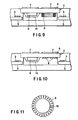
- FIG. 9 shows an example of mounting, in which the first coupler coil 8 is wound near the IC chip 6.
- the IC chip 6 is eccentrically mounted on the module substrate 9.
- the first coupler coil 8 formed separately by using a winding machine (not shown) is attached to the module substrate 9 of the IC module 2 which has been fabricated up to the step of forming the seal resin 16.
- Connection terminals (not shown) of the first coupler coil 8 are connected to a predetermined circuit pattern (not shown) on the module substrate 9.
- the IC module 2 is completely fabricated.
- the step of processing the periphery of the resin seal portion to mount the first coil 8 is not required.
- the cross-sectional shape of the formed coil is rectangular with rounded corners, it may be circular or oval. The cross-sectional shape is not limited.
- FIG. 10 shows an example of mounting, in which the first coupler coil 8 is formed of a conductor print pattern on that surface of the module substrate 9, on which the IC chip 6 is mounted, such that the first coupler coil 8 is disposed near the IC chip 6.
- the connection between the module substrate 9 and first coil 8 is made simpler.
- the cross-sectional shape of the first coupler coil 8 in this embodiment is rectangular with rounded corners, it may be circular or oval.
- the cross-sectional shape is not limited. For example, as is shown in FIG. 11, if the first coupler coil 8 with a toroidal shape is wound around the periphery of the seal resin 16 of the IC chip, the directivity to the induction electromagnetic field is increased and the degree of coupling is enhanced.
- the IC module according to the second embodiment has functions compatible with both the contact-type system with external terminals and the non-contact-type system with non-contact coupling elements such as an antenna coil.
- non-contact coupling elements such as an antenna coil.
- the inside diameter of the second coupler coil of the non-contact-transmission antenna element is made greater than the outside diameter of the engagement hole for the IC module, the first coupler coil disposed on the IC module is formed on the back surface of the module substrate, and the first and second coupler coils are disposed in substantially the same plane. Thereby, the gap is reduced and a higher coupling coefficient is obtained.
- the reception sensitivity of the card is enhanced, the communication distance is increased and/or the transmission output of the external read/write apparatus can be reduced. This is convenient for the non-contact transmission function because the transmission output is restricted by the Wireless Conducty Act.
- the inside of the second coupler coil of the non-contact-transmission antenna element serves as the engagement hole for the IC module.
- the second coupler coil is disposed below the engagement hole for the IC module, there is no need to consider depth precision in forming the engagement hole.
- Conventional equipment for forming an engagement hole in an IC card with external terminals can be applied as it is.
- no connection is required between the IC module and the antenna circuit built in the card substrate. Even if a mechanical stress such as a bending stress acts on the card, there is little possibility of fault due to breakage of connection terminals, because of the absence of any contact point between the IC module and the antenna circuit.
- the second coupler coil of the non-contact-transmission antenna element is disposed outside the antenna loop, projection of the antenna coil to the embossing region is prevented.
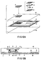
- An equivalent circuit of a non-contact coupling circuit according to an unclaimed embodiment is the same as that according to the first arrangement, as shown in FIG. 2.
- FIGS. 12A and 12B show schematic structures of the smart card according to the embodiment.
- FIG. 12A shows the whole structure and
- FIG. 12B shows a cross-sectional structure of the mounting portion of the IC module.
- the smart card 1 according to this unclaimed embodiment comprises the IC module 2 and the card substrate 10 wherein the antenna substrate 5 having the second coupler coil 3 and the antenna coil 4 formed of print coils on a resin sheet surface is resin-sealed.
- the IC module 2 comprises the patterned terminal electrodes 7 serving as a contact-type transmission section; the IC chip 6 incorporating a contact-type interface and a non-contact-type interface (not shown); the first coupler coil 8 of a non-contact-type transmission section which is formed of an insulation-coated conductor wire around the IC chip 6 or module substrate 9; and the module substrate 9.
- This bonding is also realized by wire-bonding the circuit formation surface of the IC chip 6 and the module substrate 9.
- the IC chip 6 is mounted on the module substrate 9, and circuit connection is carried out. Then, the IC chip 6 is sealed with the seal resin 16. Following this, an insulation-coated conductor wire is wounded around the periphery of the IC chip 6 or the periphery of the module substrate 9, and the circuit pattern on the module substrate 9 and the terminals of the first coupler coil 8 are connected and the IC module 2 is completely fabricated.
- FIG. 12B shows a case where the first coupler coil 8 is wound around the seal resin 16 of the IC chip 6.
- the smart card 1 according to this unclaimed embodiment is fabricated in the following manner.
- the flexible antenna substrate 5 is prepared, wherein the second coupler coil 3, antenna coil 4 and capacitive element 15 are formed of print coils on the resin substrate.
- the second coupler coil 3 and antenna coil 4 may be formed of insulation-coated wire.
- Vinyl chloride is used as the resin material of the antenna substrate 5.
- polyimide, polycarbonate, or PET may be applied. The material is not limited to one kind.
- the card substrate 10 is formed.
- the second coupler coil 3 is positioned to overlap the position of mounting of the IC module 2.
- the engagement hole 11 for the IC module 2 is formed simultaneously with the formation of the card substrate 10 by the injection molding.
- the IC module 2 is bonded in the engagement hole 11 for IC module 2 in the card substrate 10 and the fabrication of the smart card 1 is completed.
- vinyl chloride is used as the material of the card substrate 10, any material such as polycarbonate may be applicable to the present invention if adequate characteristics of the card are obtained.
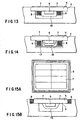
- FIG. 13 shows an example of mounting, wherein the first coupler coil 8 is wound around the IC chip 6.
- the periphery of the seal resin 16 of the IC module 2, which has been formed up to the step of formation of the seal resin 16, is processed by cutting means, etc. so as to facilitate winding of a coil.
- a coil is directly wound around the resin seal 16 of the IC module by using a winding device (not shown).
- the insulation coating (not shown) of the connection terminals of the first coupler coil 8 are removed and the connection terminals are connected to a predetermined circuit pattern (not shown) on the module substrate 9.
- the step of cutting the seal resin 16 can be omitted by forming the seal resin 16 with use of a mold, etc. which facilitates the winding of the coil.
- the coil may not be directly wound around the periphery of the IC chip 6, and a planar coil may be formed in a different step using a coil winding machine and attached to the module substrate 9 to produce the first coupler coil 8.
- the cross-sectional shape of the formed coil is rectangular with rounded corners, but it may be circular or oval.
- the cross-sectional shape is not limited.
- the first coupler coil 8 with a toroidal shape may be wound around the periphery of the seal resin 16 of the IC chip.
- FIG. 14 shows an example of mounting, wherein the first coupler coil 8 wound around a coil frame 17, which is provided around the seal resin 16 of IC chip 6, is mounted.
- the coil frame 17 is provided with terminals for connection with the coil and thereby the connection between the module substrate 9 and first coil 8 is made simpler.
- the cross-sectional shape of the coil frame 17 in this unclaimed embodiment is rectangular with rounded corners, it may be circular, etc., as with the above-described cases.
- FIGS. 15A and 15B show an example of mounting, wherein the first coupler coil 8 is wound around end faces of the module substrate 9.
- the first coupler coil 8 can also be formed by applying a coil to the periphery (in thickness direction) of the module substrate 9 of the IC module 2 with rounded corners.
- the winding of the coil around the periphery of the module substrate 9 was carried out prior to the mounting of the IC chip 6. This step may be carried out after the fabrication of the IC module 2, and the order of steps is not limited.
- the smart card according to the unclaimed embodiment has functions compatible with both the contact-type system with external terminals and the non-contact-type system with non-contact coupling elements such as an antenna coil.
- the smart card incorporating the IC module since transformer-coupling circuit elements are disposed between the IC module and antenna coil, power reception and signal transmission/reception can be effected between the IC module and antenna coil without electrical connection.
- the transformer coupling element of the IC module is realized by a coil and the coil is directly wound around the periphery of the seal resin of the IC chip.
- the planar coil prepared in advance is directly bonded to the module substrate.
- a coil is wound around the coil frame and the coil frame is bonded to the module substrate, or the coil is wound around the end faces of the module substrate.
- the number of turns of the coupler coil of the module substrate is increased as much as possible.
- electromagnetic energy received by the antenna coil can be transmitted to the IC chip by transformer coupling with a high coupling coefficient.
- the reception sensitivity of the card is enhanced, the communication distance is increased and/or the transmission output of the external read/write apparatus can be reduced. This is convenient for IC cards since the transmission output for non-contact type IC cards (smart cards) is restricted by the Wireless Conducty Act.
- a smart card and an IC module wherein, despite no connection being required between the IC module and non-contact transmission antenna coil, a reception sensitivity capable of obtaining an adequate communication distance is attained and both a contact-type and a non-contact-type transmission mechanism are maintained in practical operation states.
- the capacitive element constituting the resonance circuit along with the antenna coil 4 of the non-contact transmission mechanism.
- the chip capacitor itself or the wiring pattern on the substrate on which electronic circuits are mounted may easily be broken if a bending force, etc. acts on the card. Consequently, the reliability of the IC card deteriorates, and the IC card becomes thicker due to the thickness of the chip capacitor component.
- the coil is formed of conductor wire, the handling of the coil requires care so as not to cause deformation in the coil and problems with manufacture tend to arise.
- the capacitive element is formed of conductors sandwiching the card substrate.
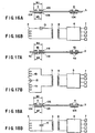
- FIG. 16A is a cross-sectional view of the same card substrate as is shown in FIGS. 3B, 8B and 12B.
- FIG. 16B shows an equivalent circuit of the card substrate shown in FIG. 16A.
- An antenna coil 4 realized as a wiring pattern using a conductive material is disposed on a peripheral portion of one surface of the substrate 5. Only one end of the antenna coil 4 is connected to one end of the second coupler coil 3, and the other end of the antenna coil 4 is opened.
- the other end of the second coupler coil 3 is guided to the other surface of the substrate 5 and connected to a conductor 104 formed of a conductive material on the other surface of the substrate 5 so as to be opposed to the antenna coil 4.
- a static capacitance is constituted by a pattern of conductive material forming the antenna coil 4 on the one surface, and the conductor 104 formed of conductive material on the other surface.
- a series capacitive element 15 in the equivalent circuit shown in FIG. 16B is obtained.
- the width Wa of the antenna coil 4 and the width Wb of the conductor 104 should not necessarily be made exactly equal, if a necessary static capacitance is obtained. However, it is desirable, as a minimum requirement, that end faces 108 of the conductor 104, the width between which is Wb, be disposed so as not to project out from end faces 106 of the antenna coil 4, the width between which is Wa. This can prevent a decrease in the coil area provided by the antenna coil 4.
- the number of turns of the antenna coil 4 is two.
- the number of turns of the antenna coil 4 and the pattern width thereof are determined in accordance with a necessary inductance and static capacitance. Since the other end of the antenna coil 4 can be opened at a desired location, the inductance of the antenna coil 4, the number of turns of which is one or more, can be adjusted by the length of the pattern of the antenna coil 4. On the other hand, needless to say, the area of the conductor 104 opposed to the antenna coil 4 can be freely set to obtain a necessary static capacitance. Therefore, compared to the conventional method in which the inductance of the coil can be adjusted only by the area of the coil and the number of turns thereof, the inductance and static capacitance can be easily adjusted.
- FIG. 17A is a cross-sectional view of the same card substrate as is shown in FIGS. 3B, 8B and 12B.
- FIG. 17B shows an equivalent circuit of the card substrate shown in FIG. 17A.
- a second antenna coil 4b realized as a wiring pattern using a conductive material is disposed on a peripheral portion of one surface of the substrate 5.
- One end of the second antenna coil 4b is connected to the second coupler coil 3, and the other end of the second antenna coil 4b is opened.
- the other end of the second coupler coil 3 is guided to the other surface of the substrate 5 and connected to one end of a first antenna coil 4a which is realized as a wiring pattern using a conductive material on the other surface of the substrate 5 so as to be opposed to the second antenna coil 4b.
- the other end of the first antenna coil 4a is disposed to be opened.
- a static capacitance is constituted by the pattern of conductive material forming the second antenna coil 4b on the one surface, and the pattern of conductive material forming the first antenna coil 4a on the other surface.
- the series capacitive element 15 in the equivalent circuit shown in FIG. 17B is obtained.
- the width Wc of the second antenna coil 4b and the width Wd of the first antenna coil 4a should not necessarily be made exactly equal, if a necessary static capacitance is obtained.
- the number of turns of the antenna coils 4a, 4b is two.
- the number of turns of the second antenna coil 4b and first antenna coil 4a, and the pattern widths thereof are determined in accordance with a necessary inductance and static capacitance. Since the other end of the second antenna coil 4b and the other end of the first antenna coil 4a can be opened at desired locations, the inductance of the second antenna coil 4b can be adjusted by the length of the pattern of the second antenna coil 4b and the inductance of the first antenna coil 4a can be adjusted by the length of the pattern of the first antenna coil 4a.
- the static capacitance increases in accordance with an area with which the second antenna coil 4b is opposed to the first antenna coil 4a, it is necessary to provide such an area with which the second antenna coil 4b is opposed to the first antenna coil 4a. Therefore, compared to the conventional method in which the inductance of the coil can be adjusted only by the area of the coil and the number of turns thereof, the inductance and static capacitance can be easily adjusted.
- FIG. 18A is a cross-sectional view of the same card substrate as is shown in FIGS. 3B, 8B and 12B.
- FIG. 18B shows an equivalent circuit of the card substrate shown in FIG. 18A.
- the antenna coil 4 realized as a wiring pattern using a conductive material is disposed on a peripheral portion of one surface of the substrate 5.
- One end of the antenna coil 4 is connected to one end of the second coupler coil 3, and the other end of the antenna coil 4 is connected to the other end of the second coupler coil 3.
- a conductor 124 using a conductor material is disposed on the other surface of the substrate 5 so as to be opposed to the antenna coil 4.
- the width We of the antenna coil 4 and the width Wf of the conductor 124 should not necessarily be made exactly equal, if a necessary static capacitance is obtained. However, it is desirable, as a minimum requirement, that end faces 128 of the conductor 124, the width between which is Wf, be disposed so as not to project out from end faces 126 of the antenna coil 4, the width between which is We. This can prevent a decrease in the coil area provided by the antenna coil 4.
- the number of turns of the antenna coil 4 is two.
- the number of turns of the antenna coil 4 and the pattern width thereof are determined in accordance with a necessary inductance and static capacitance.
Landscapes
- Engineering & Computer Science (AREA)
- Physics & Mathematics (AREA)
- Microelectronics & Electronic Packaging (AREA)
- Computer Hardware Design (AREA)
- General Physics & Mathematics (AREA)
- Theoretical Computer Science (AREA)
- Computer Networks & Wireless Communication (AREA)
- Electromagnetism (AREA)
- Toxicology (AREA)
- Health & Medical Sciences (AREA)
- Artificial Intelligence (AREA)
- Computer Vision & Pattern Recognition (AREA)
- General Health & Medical Sciences (AREA)
- Credit Cards Or The Like (AREA)
Abstract
Description
- The present invention relates to a smart card having both a function of a contact type in which reception of supply power, transmission/reception of signals, etc. are performed via an electrical contact, and a function of a non-contact type in which reception of supply power, transmission/reception of signals, etc. are performed without provision of an electrical contact, in an information recording medium represented by IC cards, etc. used in fields such as office automation (OA), factory automation (FA) or security.
- With the advent of IC cards including semiconductor memories, etc., information recording media with greatly increased memory capacities, compared to conventional magnetic cards, etc., have been realized. In addition, with internal provision of a semiconductor integrated circuit device such as a microcomputer, an IC card itself has an arithmetic process function and this provides high security to the information recording medium.
- The IC cards are internationally standardized by the ISO (International Organization for Standardization). In general, in an IC card, an IC such as a semiconductor memory is built in a card body formed of a plastic material as a basic material and metallic conductive terminal electrodes are provided on a card surface for connection with an external read/write apparatus. In order to effect data communication between the IC card and external read/write apparatus, the IC card is inserted in a card slot of the external read/write apparatus and the terminal electrodes of the IC card are connected to the external read/write apparatus.
- This is suitable for uses requiring security and safety for communication as in large-volume data exchange and banking processing, for example, uses for crediting and electronic wallets.
- On the other hand, when the IC card is applied to gate management for entrance/exit, etc., the main purpose for communication is identification and in most cases the amount of communication data is small. Accordingly, simple processing is desired. To solve this problem, a non-contact type IC card has been devised.
- With this type of IC card, an oscillation energy field of high-frequency electromagnetism, ultrasonics, light, etc. is provided in the space. The energy is absorbed and converted to an AC power. The AC power is rectified to a DC source for driving an electronic circuit provided in the card. The frequency of an AC component in the field may be used as it is, or multiplied or divided to produce an identification signal. The identification signal is transmitted as data to an information processing circuit formed of a semiconductor device via a coupler such as an antenna coil or a capacitive element.
- In particular, most of non-contact type IC cards designed for identification or simple numerical data processing are associated with Radio Frequency Identification (RF-ID) of a hard logic which does not have a battery cell and a CPU (Central Processing Unit). With the advent of the non-contact type IC card, safety from forgery or falsification is enhanced, compared with magnetic cards. Moreover, when a carrier of the card passes through a gate, it should suffice if the carrier approaches the card to an antenna unit of the read/write apparatus attached to the gate apparatus or brings the card into contact with the antenna unit of the read/write apparatus. The carrier does not have to do time-consuming operations of taking the card out of the case and inserting it in the slot in the read/write apparatus.
- Recently, in order to apply a single card to many purposes, a smart card has been devised which has the former contact type function with external terminals and the latter non-contact type function with radiofrequency data communication. This smart card has advantages of both types, i.e. high security of the contact type which is realized by CPU processing and convenience of the non-contact type. In either the non-contact type or the composite type, where a power supply is provided in the IC card, there is no need to obtain power from the aforementioned oscillation energy field in the space.
- A general mounting method for the smart card will be described blow.
- A metallic foil antenna coil for non-contact transmission, which is formed by etching, is sandwiched between a sheet with engagement hole for an IC module and a substrate. The structure is laminated to produce a card body. In this case, two antenna terminals for connection between the antenna coil and the IC module are exposed to an inside of the engagement hole in the card body.
- Metallic terminal electrodes for connection with an external apparatus are provided on one surface of the IC module. The other surface is provided with an IC and terminals for connection with the antenna. A conductive adhesive is applied to the terminals. The IC module is mounted in the engagement hole in the card body such that the terminals with the conductive adhesive may overlap the antenna terminals of the card, and then the terminals of the IC module are connected to the antenna terminals with heat and pressure. Thus, the mounting is completed.
- This mounting method is relatively simple. However, it is difficult to confirm the state of the connection portion between the IC module and antenna, and a problem remains with the reliability of connection. In addition, degradation in the connection portion may easily occur due to mechanical stress. Moreover, since a step for applying the conductive adhesive and a thermocompression step are required for the connection between the IC module and antenna, it is difficult to use an apparatus for manufacturing a conventional IC card with external terminals. It is thus necessary to provide a new manufacturing line.
- In addition, in most of IC cards with the non-contact-type transmission mechanism, an emboss or a magnetic stripe cannot be applied due to restrictions of the coil shape, etc. for keeping reception power. In order to fully meet a demand on the market, the emboss and magnetic stripe have to be considered. Techniques which do not permit provision of an emboss or a magnetic stripe are restricted in the range of application.
- A non-contact-type IC card disclosed, for example, in Jpn. Pat. Appln. KOKAI Publication No. 8-227,447 permits provision of an emboss and a magnetic stripe. Specifically, a non-contact-type IC card having an outer shape according to ISO 7811 is provided. In order to provide a magnetic stripe and an emboss on the card, a communication IC module is constructed such that an IC mount portion, a power receiving coil and a data transmission/reception coil are arranged in a longitudinal direction on a region excluding the magnetic stripe region and embossing region.
- The reception coil and communication coil of the communication IC module are comprised of single-layer coils formed by electrocasting. Both are buried in a single strip-like substrate. Lead portions for connection with pads of the IC chip are formed of each coil.
- The IC chip is mounted on the strip-like substrate such that a circuit surface of the IC chip is opposed to the strip-like substrate. The lead portions are bump-bonded to the IC pads and a gap between the strip-like substrate and IC chip is filled with a potting resin for fixation. An inner end portion of the coil and an end portion of an internal-end lead are jumper-bonded by an enamel copper wire. The bonding is effected by instantaneous thermocompression and terminal portions are protected with potting resin.
- A method of integrating this communication IC module and the card is described. According to this method, there are provided a first sheet for covering the upper surface, a second sheet having the same thickness as the strip-like substrate and having a window with a strip-like outer shape, a third sheet having a window for passing the IC chip and a window for passing a first jumper-bonding portion, a fourth sheet having only a window for passing the IC chip, and a fifth sheet for covering the lower surface (all formed of vinyl chloride). The communication module is sandwiched by the respective sheets and subjected to thermocompression. Thus, the communication module is integrated in the card.
- Although the above technique is applicable to the non-contact-type IC card, it is not applicable to the smart card having external terminals.
- The positions of the terminals of the card with external terminals are specified by ISO 7816. FIG. 1 shows a magnetic stripe region, an embossing region and an external terminal region specified by ISO 7816. In the smart card, an IC module is mounted on the external terminal region. In FIG. 1, in the regions indicated by hatching, mounting of an antenna for non-contact coupling is prohibited.
- ISO 7816 specifies an outer long side to be 85.47-85.72 mm, an outer short side to be 53.29-54.03 mm. The magnetic stripe region is defined in an area of 15.82 mm from the upper side. The embossing region is defined in an area of 24 mm from the lower side, 6.0 mm from the left side, and 8.0 mm from the right side. The external terminals are formed in an area of 28.55 mm from the upper side and 19.87 mm from the left side.
- For example, Jpn. Pat. Appln. KOKAI Publication No. 7-239,922 discloses a prior-art technique of a smart card realizing a magnetic stripe and embossing.
- According to this technique, the IC module for the IC card comprises an IC chip; a transmission mechanism connected to the IC chip for effecting transmission of information and/or power with the external apparatus; and a support member for supporting the IC chip and transmission mechanism. The transmission mechanism comprises a non-contact-type transmission mechanism having a coil or an antenna, and a contact-type transmission mechanism having a plurality of terminal electrodes of patterned conductors provided on a surface of the support member. This document teaches that since the functions compatible with the contact type and non-contact type are constructed as a module and this IC module is fitted and fixed in a plastic card body, the magnetic stripe and embossing can be made without hindrance.
- The document further discloses, as mounting means, that the antenna or coil for non-contact transmission is provided so as to surround the terminal electrodes, and alternatively the antenna is positioned at the center and the terminal electrodes are provided around the antenna.
- Specifically, the non-contact transmission antenna is contained in the IC module and thereby the connection between the antenna coil and the IC module is omitted in the final step.
- In view of the standard illustrated in FIG. 1, however, it is clear that the method in which the antenna coil is provided around the terminal electrodes is not feasible. More specifically, in the method in which the non-contact transmission antenna is contained in the IC module, an adequate antenna area is not obtained, and this permits only a so-called close-contact mode in which the distance for communication is several mm or less.
- Since the distance between the terminal electrodes and embossing region is 1.45 mm at maximum, it is not practical to dispose the antenna or coil so as to surround the terminal electrodes without overlapping the terminal electrodes, as will be described below. In the case where the antenna coil is disposed around the external terminals, the maximum outside diameter and minimum inside diameter of the coil are 12 mm and 9.3 mm, respectively. If the antenna coil is formed of a print pattern in this region, where the pattern width and interval are 0.15 mm and 0.1 mm respectively, the number of turns and the inductance become about four and 0.4 µH, and six and 1.0 µH in respective cases (µH denotes microhenry). Where the coil is disposed around the outer periphery of the terminal electrodes while the embossing region maintained, only several turns are obtained even with the formation of the print coil. Owing to the smallness of the area of the coil, too, adequate power cannot be obtained and only close coupling is permitted with a communication distance being several mm or less.
- In this case, the merit of adding the non-contact transmission function is small. The merit of adding the non-contact transmission mechanism to the contact type transmission mechanism is obtained with a communication distance exceeding several-ten mm to 100 mm. Communication is achieved if the card is exposed to the antenna unit of the external read/write apparatus within such an area. For this purpose, it is necessary to increase the area of the coil or the number of turns.
- In brief, where the coil is disposed around the outer periphery of the terminal electrodes within the IC module, only several turns are obtained even if the print coil is formed, and owing to the smallness of the area of the coil, too, adequate power cannot be obtained. Moreover, if a practical number of turns is to be obtained with a conductor pattern, it overlaps the embossing region.
- On the other hand, in the case of the latter mounting means wherein the terminal electrodes are disposed around the antenna, the embossing area is obviously occupied and the standard of the IC card with external terminals, ISO 7816, is not at all satisfied. The likelihood of acceptance in the market is very low.
- Since the smart card is associated with weak radio waves, there is a demand to enhance power transmission efficiency. Prior-art techniques for this purpose are described, for example, in Jpn. Pat. Appln. KOKAI Publication No. 2-7,838 and Jpn. Pat. Appln. KOKAI Publication No. 63-224,635. In these prior-art methods for enhancing the power transmission efficiency, however, attention is paid only to transmission power and these methods are effective only in cases where the transmission-side power efficiency can be improved and more power be sent out. Consequently, where the intensity of a radiant electromagnetic field is limited, these methods do not contribute to the improvement in the reception-side power reception efficiency. In order to improve the power reception performance of the smart card located in a weak electromagnetic field with the non-contact type function of the IC card itself, it is necessary to provide the card with means for absorbing more radiation energy.
- Furthermore, since the smart card includes a semiconductor integrated circuit, acquisition of more current with less power is desirable for reduction of a load on the power supply circuit. In order words, it is desirable to lower the power-reception side impedance. In the prior art, however, attention is paid only to the transmission voltage and not to the power reception side.
- FR-A-2 743 649 discloses a hybrid contact and contactless electronic module particularly adapted to the manufacture of hybrid cards. The module comprises a microcircuit and an antenna placed on a first face of a carrier substrate of the module as well as contacts being identical with contacts for contact cards and being connected to corresponding pads of the microcircuit by conductor leads. The microcircuit can communicate with the outside using the contacts or the antenna.
- DE-A-43 11 493 discloses a manufacturing unit and an identification unit in card format, e.g. a key card or credit card, manufactured by means of this manufacturing unit. The manufacturing unit comprises a module substrate, a chip and a coil forming a transponder unit, and a contact area comprising various contact regions. The transponder unit can be used for contactless identification, i.e. for contactless access to data stored on the chip. Furthermore, the contact area enables an access of a contact type from outside to the transponder unit.
- DE-A-195 16 227 discloses a contactless chip card using inductive coupling to connect to a terminal. The problems caused when integrating an antenna into the chip card so as to achieve a contactless connection to a terminal are discussed. It is suggested to provide a first coil around a semiconductor chip. The first coil can be disposed on a carrier element, together with the semiconductor chip. The chip card also has a second coil forming a small loop. The small loop runs at a small distance from the first coil and is inductively coupled to the same.
- It is an object of the present invention to overcome problems in the prior art and to provide a smart card having reception sensitivity enough to obtain an adequate communication distance, despite no wired connection disposed between an IC module and an antenna, and being capable of maintaining both a contact-type and a non-contact-type transmission mechanism in practical operation states.
- This object is achieved by a smart card as outlined in the attached claims.
-
- FIG. 1 shows dimensions of a card with an external terminal, as stipulated by ISO 7816;
- FIG. 2 shows an equivalent circuit of a non-contact coupler circuit for describing the principle of a non-contact transmission mechanism according to the present invention;
- FIG. 3A and FIG. 3B are an exploded perspective view and a cross-sectional view showing a structure of a first arrangement of a smart card not forming part of the present invention;
- FIG. 4 shows a first example of arrangement of an antenna coil according to the first arrangement;
- FIG. 5 shows a second example of arrangement of the antenna coil according to a first embodiment;
- FIG. 6 shows a third example of arrangement of the antenna coil which is not claimed;
- FIG. 7 shows a fourth example of arrangement of the antenna coil according to the first embodiment;
- FIG. 8A and FIG. 8B are an exploded perspective view and a cross-sectional view showing a structure of a second embodiment of a smart card according to the present invention;
- FIG. 9 shows a first example of arrangement of an antenna coil according to the second embodiment;
- FIG. 10 shows a second example of arrangement of the antenna coil according to the second embodiment;
- FIG. 11 shows a third example of arrangement of the antenna coil according to the second embodiment;
- FIG. 12A and FIG. 12B are an exploded perspective view and a cross-sectional view showing a structure of an unclaimed embodiment of a smart card;
- FIG. 13 shows a first example of arrangement of an antenna coil according to the unclaimed embodiment;
- FIG. 14 shows a second example of arrangement of the antenna coil according to the unclaimed embodiment;
- FIG. 15A and FIG. 15B show a third example of arrangement of the antenna coil according to the unclaimed embodiment;
- FIG. 16A and FIG. 16B show a first example of the structure of a capacitive element;
- FIG. 17A and FIG. 17B show a second example of the structure of the capacitive element; and
- FIG. 18A and FIG. 18B show a third example of the structure of the capacitive element.
-
- Embodiments of the smart card will now be described with reference to the accompanying drawings.
- To begin with, the basic structure and basic principle of a non-contact transmission mechanism will be described.
- FIG. 2 shows an equivalent circuit of a non-contact coupler circuit for describing the principle of the non-contact transmission mechanism. A transmission/
reception circuit 101 of a non-contact type external read/write apparatus 100 is connected to a transmission/reception coil 102 which is an electromagnetic coupler for supplying power to, and exchanging information with, the non-contact transmission mechanism in the smart card. - On the other hand, the non-contact transmission mechanism of the
smart card 1 comprises anantenna coil 4, connected electromagnetically and directly to the transmission/reception antenna 102 of the external read/write apparatus 100, for receiving power and exchanging information; acapacitive element 15 connected between both ends of theantenna coil 4 to constitute a parallel resonance circuit; anIC chip 6 mounted on anIC module 2; afirst coupler coil 8 connected to theIC chip 6; and asecond coupler coil 3 closely coupled and disposed to transmit a signal received by theantenna coil 4 to thefirst coupler coil 8 with a maximum efficiency and connected between both ends of thecapacitive element 15 of the parallel resonance circuit. - Although the
capacitive element 15 is connected in parallel to theantenna coil 4, it may preferably be connected in series between theantenna coil 4 andsecond coupler coil 3. If the parasitic capacity is increased, thecapacitive element 15 can be dispensed with. - Coupling among the respective coils will now be described, referring to a case where power and information is transmitted from the external read/
write apparatus 100 to thesmart card 1. - A high-frequency magnetic field is induced in the transmission/
reception coil 102 by a high-frequency signal (not shown) produced by the transmission/reception circuit 101 of the external read/write apparatus 100. This high-frequency signal is radiated to the space as magnetic energy. - If the
smart card 1 is located in the high-frequency magnetic field at this time, a current is caused to flow in the parallel resonance circuit, which comprises theantenna coil 4 andcapacitive element 15 of thesmart card 1, due to the high-frequency magnetic field produced by the transmission/reception coil 102 of the external read/write apparatus 100. In this case, currents due to the high-frequency magnetic field are also induced in thefirst coupler coil 8 connected directly to theIC chip 6 and thesecond coupler coil 3 connected to the resonance circuit of theantenna coil 4 andcapacitive element 15 to transmit power to thefirst coupler coil 8. The amount of induced currents in this case is less than that of current induced in theantenna coil 4 by an order of magnitude, and accordingly the sensitivity of reception depends greatly on characteristics of theantenna coil 4. - A signal received by the resonance circuit of the
antenna coil 4 andcapacitive element 15 is transmitted to thesecond coupler coil 3. Since thesecond coupler coil 3 andfirst coupler coil 8 are closely coupled and disposed with a maximum transmission efficiency, the signal is then transmitted to theIC chip 6 via transformer coupling of thesecond coupler coil 3 andfirst coupler coil 8. The maximum transmission efficiency of transformer coupling between thesecond coupler coil 3 andfirst coupler coil 8 is determined by selection of the circuit constant. - With the above structure, the reception characteristics are improved. As a result, the characteristics of the
antenna coil 4 determine the sensitivity of reception. Thus, the larger the area of theantenna coil 4, the greater the advantage. - The antenna characteristics vary depending on the method of the non-contact transmission mechanism, such as electromagnetic coupling, electromagnetic induction, etc.. The antenna coil characteristics with the electromagnetic induction method in a short-wave band are calculated, for example, as shown in TABLE 1.
Example COIL AREA (LONG SIDE × SHORT SIDE) NUMBER OF COIL TURNS INDUCTANCE 5µH INDUCTANCE 20 µH 1 84 mm × 53 mm 4 turns 10 turns 2 84 mm × 37 mm 5 turns 11 turns 3 64 mm × 28 mm 6 turns 14 turns 4 64 mm × 13 mm 7 turns 16 turns 5 12 mm × 12 mm 15 turns*1 30 turns - In TABLE 1, the thickness and pitch of the coil are 0.05 mm in the case of *1 alone. In the other cases, the thickness and pitch of the coil are 0.15 mm.
- For instance, the inductance of the antenna coil of the currently used RF-ID card for the short-wave band is about 5 microhenries. This type of antenna coil can be disposed on an outer peripheral portion of the card by means of a print pattern (print coil).
- Referring back to FIG. 1, at the lower part of the card, the distance between the embossing region and the periphery of the card takes a minimum value, i.e. 2.41 mm. If a spiral coil is formed from a point, which is 1 mm inside the edge of the card, toward the center of the card, with the pattern width and the pattern interval being set at 0.15 mm, the spiral coil can have five turns at maximum. Where the pattern width and the pattern interval are set at 0.1 mm, the coil can have seven turns at maximum.
- Fifteen turns are required to obtain an inductance of 5 microhenries, if an antenna coil is provided around the external terminals of the IC module, as in the prior-art technique of Jpn. Pat. Appln. KOKAI Publication No. 7-239,922, and the coil is disposed at the width of 1.45 mm as specified by the Standard. In this case, both the pattern width and interval have to be set at 0.05 mm or less, and this is unrealizable.
- On the other hand, in the case of an antenna coil of a low-frequency electromagnetic coupling system, the number of turns exceeding seven may be required.
- Consider a structure requiring an antenna coil having an inductance of, e.g. 20 microhenries. In this case, it is understood, from TABLE 1, that coils having 10 to 30 turns can be obtained according to the coil area.
- Coils having more than eight turns can be realized by a spiral coil of a three-dimensional shape and a planer print coil. In the case of the spiral coil, it is wound in an overlapping manner and thus can be disposed at an outer peripheral portion of the card. In the case of the print coil, it is generally formed in a non-overlapping manner. Accordingly, where the number of turns is large, it is not proper to dispose the coil at the outer peripheral portion of the card so as to avoid overlapping with the embossing region.
- In this case, if the antenna coil is disposed such that mounting prohibition areas of the magnetic stripe, embossing and external terminals may not be included inside the antenna coil, the card can be fabricated at low cost with simple manufacturing process and with high reliability.
- FIG. 3A and FIG. 3B show a schematic structure of a smart card according to a first arrangement. FIG. 3A shows the whole structure and FIG. 3B shows a cross-sectional structure of the mounting portion of the IC module.
- The
smart card 1 according to this arrangement comprisescard substrates 10 resin-seal anantenna substrate 5 which includes anIC module 2, asecond coupler coil 3 and anantenna coil 4 formed of print coils on a resin sheet surface of theantenna substrate 5. TheIC module 2 comprises anIC chip 6 incorporating a contact-type interface and a non-contact-type interface (not shown) and amodule substrate 9 havingterminal electrodes 7 serving as a contact-type transmission section and afirst coupler coil 8 of a non-contact-type transmission section which are formed on different surfaces by patterning. - Instead of forming the
first coupler coil 8 andantenna coil 4 of print coils, they may be formed by winding insulation-coated conductor wires. TheIC chip 6 is mounted on the surface ofmodule substrate 9, on which thefirst coupler coil 8 is formed. TheIC chip 6 is connected to theterminal electrodes 7 ofmodule substrate 9 via through-holes. - The
IC chip 6 and a circuit pattern offirst coupler coil 8 are wire-bonded to constitute a circuit. This bonding may also be realized by thermal fusion using solder or conductive adhesive, which is applied to the circuit formation surface of the IC chip and the substrate. - The
IC chip 6 is mounted on the module substrate, and circuit connection is carried out. Then, theIC chip 6 is resin-sealed and the fabrication of theIC module 2 is completed. - In general terms, the
smart card 1 according to the present arrangement is fabricated in a manner described below. - To start with, the
flexible antenna substrate 5 having thesecond coupler coil 3,antenna coil 4 andcapacitive element 15 formed of print coils on a resin substrate is prepared. Thesecond coupler coil 3 andantenna coil 4 may be formed by winding insulation-coated conductor wires. The resin material of theantenna substrate 5 may be vinyl chloride, or polyimide, polycarbonate, or PET. The material is not limited to one kind. - The
antenna substrate 5 is sealed by injection molding to form thecard substrate 10. In the formation, thesecond coupler coil 3 is positioned to overlap the mounting position of theIC module 2. Simultaneous with the fabrication of thecard substrate 10 by means of injection molding, anengagement hole 11 for theIC module 2 is formed. - At last, the
IC module 2 is attached in theengagement hole 11 in thecard substrate 10 for engagement with theIC module 2, and fabrication of thesmart card 1 is completed. The card substrate is formed of vinyl chloride, but other materials such as polycarbonate are applicable to the present invention if characteristics of the card such as adequate strength and embossing processability are obtained. - In FIG. 3A, the
card substrate 10 is shown as being divided into an obverse side portion and a reverse side portion. However, thecard substrate 10 is actually a single piece. In the figure, the card substrate is shown in a modified fashion in order to clearly describe a relationship between the coupler coil andengagement hole 11 of theantenna substrate 5 which is sealed in the card substrate. - In the present arrangement, the card is fabricated by injection molding. Any method, however, is applicable if characteristics of embossing are maintained. For instance, a laminating method or an adhesive filling method may be adopted. In this arrangement, the
engagement hole 11 for the IC module is made by cutting after the fabrication of the card. - FIG. 4 is a plan view of the first arrangement of the smart card having an embossing region, showing a position of mounting of the
antenna coil 4 within thesmart card 1. Theantenna coil 4 is disposed over the entire peripheral portion of the card. Theembossing region 20 and externalterminal region 21 are disposed within the loop of theantenna coil 4. The specifications of this coil correspond to example 1 in TABLE 1. - The example of FIG. 4 is effective where the number of turns of
antenna coil 4 is relatively small, specifically, 3 to 7, and preferably 4 or 5. As regards theantenna substrate 5 in this example of mounting, that portion of the resin sheet, which corresponds to theembossing region 20, is cut out. This aims at preventing an adverse effect on embossing characteristics. - In FIGS. 4 to 7, the outer contours of the
antenna substrates 5 are indicated by broken lines. - FIG. 5 is a plan view of another
smart card 1 according to a first embodiment of the invention having the embossing region. This figure shows a general shape of theantenna coil 4, on the outside of which theembossing region 20 and externalterminal region 21 are disposed (i.e. not within the antenna coil). The specifications of this coil correspond to example 3 in TABLE 1. The example of FIG. 5 is effective where the number of turns of theantenna coil 4 is 10 or more. - FIG. 6 is a plan view of a third example of mounting of the
smart card 1 according to the first arrangement, which has both the magnetic stripe and embossing region. This figure shows a position of mounting of theantenna coil 4 in thesmart card 1. Theantenna coil 4 is made not to overlap themagnetic stripe region 22. That portion of the antenna coil, which excludes a portion thereof opposed to the magnetic stripe region, is disposed along the outer periphery of thesmart card 1. The specifications of this coil correspond to example 2 in TABLE 1. As regards theantenna substrate 5 in this example of mounting, too, that portion of the resin sheet, which corresponds to theembossing region 20, is cut out. This aims at preventing an adverse effect on embossing characteristics. - FIG. 7 is a plan view of a fourth example of mounting of the
smart card 1 according to the first embodiment of the invention, which has both the magnetic stripe and embossing region. This figure shows a general shape of theantenna coil 4 which is disposed not to include theembossing region 20 ormagnetic stripe region 22. The specifications of this coil correspond to example 4 in TABLE 1. - The smart card according to the first arrangement has functions compatible with both the contact-type system with external terminals and the non-contact-type system with non-contact coupling elements such as an antenna coil. By providing the IC module and antenna coil with transformer-coupling circuit elements, power reception and signal transmission/reception can be effected between the IC module and antenna coil without electrical connection.
- With this structure, the area of the antenna coil is increased to a maximum permissible level. When the card is exposed to the vicinity of the antenna of the external read/write apparatus, communicable sensitivity characteristics can be maintained, which is the advantage of the non-contact communication function.
- Since the reception sensitivity of the card is enhanced, the communication distance is increased and/or the transmission output of the external read/write apparatus can be reduced. This is convenient for cards since the transmission output is restricted by the Wireless Telegraphy Act.
- Moreover, since no connection is required between the IC module and the antenna circuit built in the card substrate, it is possible to use, without any modification, the conventional IC card fabrication step of attaching and mounting the IC module in the engagement hole formed in the card substrate. Furthermore, even if a mechanical stress such as a bending stress acts on the card, there is little possibility of fault because of the absence of any contact point between the IC module and the antenna circuit.
- Since the antenna coil which is directly brought into non-contact coupling with the external read/write apparatus is so disposed as not to overlap the external terminal region of the non-contact-type electrodes, which is also the IC module engagement region, the embossing region and/or the magnetic stripe region, this invention permits general-purpose applications and is fully applicable to conventional cards.
- Since injection molding is adopted and the base material of the flexible antenna substrate is not present in the area corresponding to the embossing region, embossing properties are not affected by the attachment of plural sheets.
- Since the antenna substrate including the antenna coil is formed of a flexible printed wiring board and the coil is formed in a planar shape, the thickness of the card can be set to fully meet the standard of ISO 7816, i.e. 0.76 mm.
- As is understood from FIG. 2, the increase in the number of turns of the
first coupler coil 8 increases a coefficient of coupling with thesecond coupler coil 3, and energy to be transmitted to theIC chip 6 further increases. In the current technique for fabricating printed wiring boards, the limit pattern width is 0.1 mm. It is difficult to form several-ten turns of a print coil in the module substrate of the IC card. On the other hand, where a coil is formed of an insulation-coated conductor wire, a diameter of several-ten microns is attained by virtue of development in magnetic head technology. In the present arrangement, paying attention to this technology, the coupler coils for the IC module and antenna may be formed of an insulation-coated conductor wire. - As has been described above, according to the present arrangement, there is provided a smart card wherein no connection is required between the IC module and non-contact transmission antenna coil, a reception sensitivity capable of obtaining an adequate communication distance is attained, the IC card is compatible with both embossing processing and magnetic stripe formation, and both a contact-type and a non-contact-type transmission mechanisms are maintained in practical operation states.
- Other embodiments of the smart card will now be described. In the descriptions of the other embodiments, those elements common with the first arrangement are denoted by like reference numerals, and a description thereof is omitted.
- An equivalent circuit of a non-contact coupling circuit according to a second embodiment is the same as that according to the first arrangement, as shown in FIG. 2.
- In a case of an air-core transformer type coupling as illustrated in FIG. 2, a reduction of a gap between coils increases transmission efficiency. Unlike the first arrangement in which the first and second coupler coils are vertically arranged, the inside diameter of the second coupler coil, in the second embodiment, is made larger than the engagement hole for the
IC module 2 in a card substrate (not shown). Thefirst coupler coil 8 is surrounded by thesecond coupler coil 3, and both are substantially disposed in the same plane. At this time, the inside of thesecond coupler coil 3 serves also as the engagement hole. - Thereby, compared to the case where the
second coupler coil 3 is disposed below the engagement hole for theIC module 2, there is no need to consider depth precision in forming the engagement hole. Equipment for forming an engagement hole in an IC card with external terminals can be applied as it is. - FIGS. 8A and 8B show schematic structures of the smart card according to the second embodiment of the present invention. FIG. 8A shows the whole structure and FIG. 8B shows a cross-sectional structure of the mounting portion of the IC module.
- The
smart card 1 according to this embodiment comprises theIC module 2 of the present invention, and thecard substrate 10 wherein theantenna substrate 5 having thesecond coupler coil 3 and theantenna coil 4 formed of print coils on a resin sheet surface is resin-sealed. - The
IC module 2 comprises the patternedterminal electrodes 7 serving as a contact-type transmission section; theIC chip 6 incorporating a contact-type interface and a non-contact-type interface (not shown); thefirst coupler coil 8 of a non-contact-type transmission section which is formed of an insulation-coated conductor wire around theIC chip 6 ormodule substrate 9; and themodule substrate 9. - The
IC chip 6 is mounted on a surface of themodule substrate 9, which is opposite to a surface thereof provided with theterminal electrodes 7. TheIC chip 6 and theterminal electrodes 7 on themodule substrate 9 are connected via through-holes. TheIC chip 6 and a circuit pattern on themodule substrate 9 for connecting theterminal electrodes 7 andfirst coupler coil 8 are bonded by means of thermal fusion using solder or conductive adhesive. This bonding is also realized by wire-bonding the circuit formation surface of theIC chip 6 and themodule substrate 9. - The
IC chip 6 is mounted on themodule substrate 9, and circuit connection is carried out. Then, theIC chip 6 is sealed with aseal resin 16, as shown in FIG. 8A. Following this, an insulation-coated conductor wire is wounded around the periphery of theIC chip 6 or the periphery of themodule substrate 9, thereby forming thefirst coupler coil 8. Subsequently, the circuit pattern on themodule substrate 9 and the terminals of thefirst coupler coil 8 are connected and theIC module 2 is completely fabricated. - FIG. 8B shows a case where the
first coupler coil 8 is wound around theseal resin 16 of theIC chip 6. In preparation for the formation of thefirst coupler coil 8, the periphery of theseal resin 16 of theIC module 2, which has been formed up to the step of formation of theseal resin 16, is processed by cutting means, etc. so as to facilitate winding of a coil. Subsequently, a coil is directly wound around theresin seal 16 of the IC module by using a winding device (not shown). - After a predetermined number of turns have been wound, the insulation coating (not shown) of the connection terminals of the
first coupler coil 8 are removed and the connection terminals are connected to a predetermined circuit pattern (not shown) on themodule substrate 9. - In this case, the step of cutting the
seal resin 16 can be omitted by forming theseal resin 16 with use of a mold, etc. which facilitates the winding of the coil. This embodiment also includes a technique wherein a coil is not directly wound around the periphery of theIC chip 6 and, instead, a planar coil is formed in a different step using a coil winding machine and is attached to themodule substrate 9 to produce thefirst coupler coil 8, following which theseal resin 16 is provided to cover theIC chip 6 andfirst coupler coil 8. - In this embodiment, the cross-sectional shape of the formed coil is rectangular with rounded corners, but it may be circular. The cross-sectional shape is not limited.
- In general terms, the
smart card 1 according to this embodiment is fabricated in the following manner. - To begin with, as shown in FIGS. 8A and 8B, the
antenna substrate 5 is prepared, wherein thesecond coupler coil 3,antenna coil 4 andcapacitive element 15 are formed of print coils on different regions on the resin substrate. - As is shown in FIG. 8B, the
second coupler coil 3 on theantenna substrate 5 is formed outside theengagement hole 11 for theIC module 2. Thesecond coupler coil 3 is finally nested in substantially the same plane as thefirst coil 8 mounted in theIC module 2. Thesecond coupler coil 3 andantenna coil 4 may be formed of insulation-coated wire. - Vinyl chloride is used as the resin material of the
antenna substrate 5. However, polycarbonate, PET, or polyimide may be applied. The material is not limited to one kind. The thickness of theantenna substrate 5 is in a range of 50 µm to 300 µm, and preferably about 100 µm. - Then, by sealing the
antenna substrate 5 by injection molding, thecard substrate 10 is formed. In the molding, thesecond coupler coil 3 is positioned to overlap the position of mounting of theIC module 2. After thecard substrate 10 is formed by the injection molding, theengagement hole 11 for theIC module 2 is formed. - At last, the
IC module 2 is bonded in theengagement hole 11 forIC module 2 in thecard substrate 10 and the fabrication of thesmart card 1 is completed. Although vinyl chloride is used as the material of thecard substrate 10, any material such as polycarbonate may be applicable to the present invention if adequate characteristics of the card are obtained. In FIG. 8A, thecard substrate 10 is shown as being divided into an obverse side portion and a reverse side portion. However, thecard substrate 10 is actually a single piece. In FIG. 8A, the card substrate is shown in a modified fashion in order to clearly describe a relationship between the coupler coil andengagement hole 11 of theantenna substrate 5 which is sealed in the card substrate. - In the present embodiment, the card is fabricated by injection molding. Any method, however, is applicable to the present invention if characteristics of the card are maintained. For instance, a laminating method or an adhesive filling method may be adopted. This embodiment includes a technique wherein the
engagement hole 11 for the IC module is formed at the same time as the card is formed. In this case, the inside of thesecond coupler coil 3 on theantenna coil 5 is cut out in advance for engagement with the IC module. - FIG. 9 shows an example of mounting, in which the
first coupler coil 8 is wound near theIC chip 6. In this example, theIC chip 6 is eccentrically mounted on themodule substrate 9. Thefirst coupler coil 8 formed separately by using a winding machine (not shown) is attached to themodule substrate 9 of theIC module 2 which has been fabricated up to the step of forming theseal resin 16. Connection terminals (not shown) of thefirst coupler coil 8 are connected to a predetermined circuit pattern (not shown) on themodule substrate 9. Thus, theIC module 2 is completely fabricated. Thereby, the step of processing the periphery of the resin seal portion to mount thefirst coil 8 is not required. Although the cross-sectional shape of the formed coil is rectangular with rounded corners, it may be circular or oval. The cross-sectional shape is not limited. - FIG. 10 shows an example of mounting, in which the
first coupler coil 8 is formed of a conductor print pattern on that surface of themodule substrate 9, on which theIC chip 6 is mounted, such that thefirst coupler coil 8 is disposed near theIC chip 6. - Since the
first coupler coil 8, as well as the external terminals on the upper surface of themodule substrate 9 and theIC chip 6 on the back surface thereof, is formed simultaneously with connection patterns, the connection between themodule substrate 9 andfirst coil 8 is made simpler. Although the cross-sectional shape of thefirst coupler coil 8 in this embodiment is rectangular with rounded corners, it may be circular or oval. The cross-sectional shape is not limited. For example, as is shown in FIG. 11, if thefirst coupler coil 8 with a toroidal shape is wound around the periphery of theseal resin 16 of the IC chip, the directivity to the induction electromagnetic field is increased and the degree of coupling is enhanced. - The IC module according to the second embodiment has functions compatible with both the contact-type system with external terminals and the non-contact-type system with non-contact coupling elements such as an antenna coil. By providing the IC module and antenna coil with transformer-coupling circuit elements, power reception and signal transmission/reception can be effected between the IC module and antenna coil without electrical connection.
- In this smart card, the inside diameter of the second coupler coil of the non-contact-transmission antenna element is made greater than the outside diameter of the engagement hole for the IC module, the first coupler coil disposed on the IC module is formed on the back surface of the module substrate, and the first and second coupler coils are disposed in substantially the same plane. Thereby, the gap is reduced and a higher coupling coefficient is obtained.
- As a result, electromagnetic energy received by the antenna coil can be transmitted to the IC chip by transformer coupling with a high coupling coefficient.
- Accordingly, when the card is exposed to the vicinity of the antenna of the external read/write apparatus, communicable sensitivity characteristics can be enhanced, which is the advantage of the non-contact communication function.
- Since the reception sensitivity of the card is enhanced, the communication distance is increased and/or the transmission output of the external read/write apparatus can be reduced. This is convenient for the non-contact transmission function because the transmission output is restricted by the Wireless Telegraphy Act.
- In addition, the inside of the second coupler coil of the non-contact-transmission antenna element serves as the engagement hole for the IC module. Thereby, compared to the case where the second coupler coil is disposed below the engagement hole for the IC module, there is no need to consider depth precision in forming the engagement hole. Conventional equipment for forming an engagement hole in an IC card with external terminals can be applied as it is. Moreover, no connection is required between the IC module and the antenna circuit built in the card substrate. Even if a mechanical stress such as a bending stress acts on the card, there is little possibility of fault due to breakage of connection terminals, because of the absence of any contact point between the IC module and the antenna circuit.
- Since the second coupler coil of the non-contact-transmission antenna element is disposed outside the antenna loop, projection of the antenna coil to the embossing region is prevented.
- As has been described above, according to the second embodiment, there is provided a smart card wherein, despite no connection being required between the IC module and non-contact transmission antenna coil, a reception sensitivity capable of obtaining an adequate communication distance is attained and both a contact-type and a non-contact-type transmission mechanism are maintained in practical operation states. In addition, there is provided an IC module which is suitably applicable to this smart card.
- An equivalent circuit of a non-contact coupling circuit according to an unclaimed embodiment is the same as that according to the first arrangement, as shown in FIG. 2.
- FIGS. 12A and 12B show schematic structures of the smart card according to the embodiment. FIG. 12A shows the whole structure and FIG. 12B shows a cross-sectional structure of the mounting portion of the IC module.
- The
smart card 1 according to this unclaimed embodiment comprises theIC module 2 and thecard substrate 10 wherein theantenna substrate 5 having thesecond coupler coil 3 and theantenna coil 4 formed of print coils on a resin sheet surface is resin-sealed. - The
IC module 2 comprises the patternedterminal electrodes 7 serving as a contact-type transmission section; theIC chip 6 incorporating a contact-type interface and a non-contact-type interface (not shown); thefirst coupler coil 8 of a non-contact-type transmission section which is formed of an insulation-coated conductor wire around theIC chip 6 ormodule substrate 9; and themodule substrate 9. - The
IC chip 6 is mounted on a surface of themodule substrate 9, which is opposite to a surface thereof provided with theterminal electrodes 7. TheIC chip 6 and theterminal electrodes 7 on themodule substrate 9 are connected via through-holes. TheIC chip 6 and a circuit pattern of thefirst coupler coil 8 are bonded by means of thermal fusion using solder or conductive adhesive. - This bonding is also realized by wire-bonding the circuit formation surface of the
IC chip 6 and themodule substrate 9. - The
IC chip 6 is mounted on themodule substrate 9, and circuit connection is carried out. Then, theIC chip 6 is sealed with theseal resin 16. Following this, an insulation-coated conductor wire is wounded around the periphery of theIC chip 6 or the periphery of themodule substrate 9, and the circuit pattern on themodule substrate 9 and the terminals of thefirst coupler coil 8 are connected and theIC module 2 is completely fabricated. FIG. 12B shows a case where thefirst coupler coil 8 is wound around theseal resin 16 of theIC chip 6. - In general terms, the
smart card 1 according to this unclaimed embodiment is fabricated in the following manner. - To begin with, the
flexible antenna substrate 5 is prepared, wherein thesecond coupler coil 3,antenna coil 4 andcapacitive element 15 are formed of print coils on the resin substrate. In this case, thesecond coupler coil 3 andantenna coil 4 may be formed of insulation-coated wire. Vinyl chloride is used as the resin material of theantenna substrate 5. However, polyimide, polycarbonate, or PET may be applied. The material is not limited to one kind. - Then, by sealing the
antenna substrate 5 by injection molding, thecard substrate 10 is formed. In the molding, thesecond coupler coil 3 is positioned to overlap the position of mounting of theIC module 2. Theengagement hole 11 for theIC module 2 is formed simultaneously with the formation of thecard substrate 10 by the injection molding. At last, theIC module 2 is bonded in theengagement hole 11 forIC module 2 in thecard substrate 10 and the fabrication of thesmart card 1 is completed. Although vinyl chloride is used as the material of thecard substrate 10, any material such as polycarbonate may be applicable to the present invention if adequate characteristics of the card are obtained. - In FIG. 12A, the
card substrate 10 is shown as being divided into an obverse side portion and a reverse side portion. However, thecard substrate 10 is actually a single piece. In FIG. 12A, the card substrate is shown in a modified fashion in order to clearly describe a relationship between the coupler coil andengagement hole 11 of theantenna substrate 5 which is sealed in the card substrate. In the present embodiment, the card is fabricated by injection molding. Any method, however, is applicable if characteristics of the card are maintained. For instance, a laminating method or an adhesive filling method may be adopted. This embodiment includes a technique wherein theengagement hole 11 for the IC module is processed by cutting after the card is formed. - FIG. 13 shows an example of mounting, wherein the
first coupler coil 8 is wound around theIC chip 6. - In preparation for the formation of the
first coupler coil 8, the periphery of theseal resin 16 of theIC module 2, which has been formed up to the step of formation of theseal resin 16, is processed by cutting means, etc. so as to facilitate winding of a coil. Subsequently, a coil is directly wound around theresin seal 16 of the IC module by using a winding device (not shown). After a predetermined number of turns have been wound, the insulation coating (not shown) of the connection terminals of thefirst coupler coil 8 are removed and the connection terminals are connected to a predetermined circuit pattern (not shown) on themodule substrate 9. - In this case, the step of cutting the
seal resin 16 can be omitted by forming theseal resin 16 with use of a mold, etc. which facilitates the winding of the coil. The coil may not be directly wound around the periphery of theIC chip 6, and a planar coil may be formed in a different step using a coil winding machine and attached to themodule substrate 9 to produce thefirst coupler coil 8. - In this unclaimed embodiment, the cross-sectional shape of the formed coil is rectangular with rounded corners, but it may be circular or oval. The cross-sectional shape is not limited.
- As is shown in FIG. 11, if the
first coupler coil 8 with a toroidal shape may be wound around the periphery of theseal resin 16 of the IC chip. - FIG. 14 shows an example of mounting, wherein the
first coupler coil 8 wound around acoil frame 17, which is provided around theseal resin 16 ofIC chip 6, is mounted. - The
first coupler coil 8 is regularly wound along grooves (not shown) of thecoil frame 17. Thefirst coupler coil 8 wound around thecoil frame 17 is bonded between thecoil frame 17 andmodule substrate 9. Then, connection terminals (not shown) of thefirst coupler coil 8 are connected to a predetermined circuit pattern (not shown) on themodule substrate 9. - In this case, the
coil frame 17 is provided with terminals for connection with the coil and thereby the connection between themodule substrate 9 andfirst coil 8 is made simpler. Although the cross-sectional shape of thecoil frame 17 in this unclaimed embodiment is rectangular with rounded corners, it may be circular, etc., as with the above-described cases. - FIGS. 15A and 15B show an example of mounting, wherein the
first coupler coil 8 is wound around end faces of themodule substrate 9. - The
first coupler coil 8 can also be formed by applying a coil to the periphery (in thickness direction) of themodule substrate 9 of theIC module 2 with rounded corners. The winding of the coil around the periphery of themodule substrate 9 was carried out prior to the mounting of theIC chip 6. This step may be carried out after the fabrication of theIC module 2, and the order of steps is not limited. - In the case were the coil is applied to the periphery (in thickness direction) of the
module substrate 9 of theIC module 2 with rounded corners, the coil can be wound with a width of 1 mm from the outer contour of themodule substrate 9 if the thickness of themodule substrate 9 is 0.3 mm, even in consideration of the formation of embossing. If the diameter of the coil wire is 0.1 mm, 3 × 10 = 30 turns can be wound. This number is five times as large as in the case of forming the coil by print patterning. - The smart card according to the unclaimed embodiment has functions compatible with both the contact-type system with external terminals and the non-contact-type system with non-contact coupling elements such as an antenna coil. In the smart card incorporating the IC module, since transformer-coupling circuit elements are disposed between the IC module and antenna coil, power reception and signal transmission/reception can be effected between the IC module and antenna coil without electrical connection.
- The transformer coupling element of the IC module is realized by a coil and the coil is directly wound around the periphery of the seal resin of the IC chip. Alternatively, the planar coil prepared in advance is directly bonded to the module substrate. Alternatively, a coil is wound around the coil frame and the coil frame is bonded to the module substrate, or the coil is wound around the end faces of the module substrate. Thereby, the number of turns of the coupler coil of the module substrate is increased as much as possible. As a result, in the smart card incorporating the IC module, electromagnetic energy received by the antenna coil can be transmitted to the IC chip by transformer coupling with a high coupling coefficient.
- Accordingly, when the card is exposed to the vicinity of the antenna of the external read/write apparatus, communicable sensitivity characteristics can be enhanced, which is the advantage of the non-contact communication function.
- Since the reception sensitivity of the card is enhanced, the communication distance is increased and/or the transmission output of the external read/write apparatus can be reduced. This is convenient for IC cards since the transmission output for non-contact type IC cards (smart cards) is restricted by the Wireless Telegraphy Act.
- Moreover, since no connection is required between the IC module and the antenna circuit built in the card substrate, it is possible to use, without any modification, the conventional IC card fabrication step of attaching and mounting the IC module in the engagement hole formed in the card substrate. Furthermore, even if a mechanical stress such as a bending stress acts on the card, there is little possibility of fault because of the absence of any contact point between the IC module and the antenna circuit.
- As has been described above, according to the unclaimed embodiment, there are provided a smart card and an IC module wherein, despite no connection being required between the IC module and non-contact transmission antenna coil, a reception sensitivity capable of obtaining an adequate communication distance is attained and both a contact-type and a non-contact-type transmission mechanism are maintained in practical operation states.
- A description will now be given of a method of fabricating the capacitive element constituting the resonance circuit along with the
antenna coil 4 of the non-contact transmission mechanism. Where a chip capacitor is used as the capacitive element of the IC card, the chip capacitor itself or the wiring pattern on the substrate on which electronic circuits are mounted may easily be broken if a bending force, etc. acts on the card. Consequently, the reliability of the IC card deteriorates, and the IC card becomes thicker due to the thickness of the chip capacitor component. Moreover, since the coil is formed of conductor wire, the handling of the coil requires care so as not to cause deformation in the coil and problems with manufacture tend to arise. In the present invention, in order to overcome such problems, the capacitive element is formed of conductors sandwiching the card substrate. - FIG. 16A is a cross-sectional view of the same card substrate as is shown in FIGS. 3B, 8B and 12B. FIG. 16B shows an equivalent circuit of the card substrate shown in FIG. 16A. An
antenna coil 4 realized as a wiring pattern using a conductive material is disposed on a peripheral portion of one surface of thesubstrate 5. Only one end of theantenna coil 4 is connected to one end of thesecond coupler coil 3, and the other end of theantenna coil 4 is opened. - On the other hand, the other end of the
second coupler coil 3 is guided to the other surface of thesubstrate 5 and connected to aconductor 104 formed of a conductive material on the other surface of thesubstrate 5 so as to be opposed to theantenna coil 4. - A static capacitance is constituted by a pattern of conductive material forming the
antenna coil 4 on the one surface, and theconductor 104 formed of conductive material on the other surface. Thus, aseries capacitive element 15 in the equivalent circuit shown in FIG. 16B is obtained. - As is shown in FIG. 16A, the width Wa of the
antenna coil 4 and the width Wb of theconductor 104 should not necessarily be made exactly equal, if a necessary static capacitance is obtained. However, it is desirable, as a minimum requirement, that end faces 108 of theconductor 104, the width between which is Wb, be disposed so as not to project out from end faces 106 of theantenna coil 4, the width between which is Wa. This can prevent a decrease in the coil area provided by theantenna coil 4. - In FIG. 16A, the number of turns of the
antenna coil 4 is two. The number of turns of theantenna coil 4 and the pattern width thereof are determined in accordance with a necessary inductance and static capacitance. Since the other end of theantenna coil 4 can be opened at a desired location, the inductance of theantenna coil 4, the number of turns of which is one or more, can be adjusted by the length of the pattern of theantenna coil 4. On the other hand, needless to say, the area of theconductor 104 opposed to theantenna coil 4 can be freely set to obtain a necessary static capacitance. Therefore, compared to the conventional method in which the inductance of the coil can be adjusted only by the area of the coil and the number of turns thereof, the inductance and static capacitance can be easily adjusted. - FIG. 17A is a cross-sectional view of the same card substrate as is shown in FIGS. 3B, 8B and 12B. FIG. 17B shows an equivalent circuit of the card substrate shown in FIG. 17A. A
second antenna coil 4b realized as a wiring pattern using a conductive material is disposed on a peripheral portion of one surface of thesubstrate 5. One end of thesecond antenna coil 4b is connected to thesecond coupler coil 3, and the other end of thesecond antenna coil 4b is opened. - On the other hand, the other end of the
second coupler coil 3 is guided to the other surface of thesubstrate 5 and connected to one end of a first antenna coil 4a which is realized as a wiring pattern using a conductive material on the other surface of thesubstrate 5 so as to be opposed to thesecond antenna coil 4b. The other end of the first antenna coil 4a is disposed to be opened. - A static capacitance is constituted by the pattern of conductive material forming the
second antenna coil 4b on the one surface, and the pattern of conductive material forming the first antenna coil 4a on the other surface. Thus, theseries capacitive element 15 in the equivalent circuit shown in FIG. 17B is obtained. - As is shown in FIG. 17A, the width Wc of the
second antenna coil 4b and the width Wd of the first antenna coil 4a should not necessarily be made exactly equal, if a necessary static capacitance is obtained. However, it is desirable, as a minimum requirement, that end faces 118 of the first antenna coil 4a, the width between which is Wd, be disposed so as not to project out from end faces 116 of thesecond antenna coil 4b, the width between which is Wc. This can prevent a decrease in the coil area provided by thesecond antenna coil 4b. - In FIG. 17A, the number of turns of the
antenna coils 4a, 4b is two. The number of turns of thesecond antenna coil 4b and first antenna coil 4a, and the pattern widths thereof are determined in accordance with a necessary inductance and static capacitance. Since the other end of thesecond antenna coil 4b and the other end of the first antenna coil 4a can be opened at desired locations, the inductance of thesecond antenna coil 4b can be adjusted by the length of the pattern of thesecond antenna coil 4b and the inductance of the first antenna coil 4a can be adjusted by the length of the pattern of the first antenna coil 4a. On the other hand, needless to say, since the static capacitance increases in accordance with an area with which thesecond antenna coil 4b is opposed to the first antenna coil 4a, it is necessary to provide such an area with which thesecond antenna coil 4b is opposed to the first antenna coil 4a. Therefore, compared to the conventional method in which the inductance of the coil can be adjusted only by the area of the coil and the number of turns thereof, the inductance and static capacitance can be easily adjusted. - FIG. 18A is a cross-sectional view of the same card substrate as is shown in FIGS. 3B, 8B and 12B. FIG. 18B shows an equivalent circuit of the card substrate shown in FIG. 18A. The
antenna coil 4 realized as a wiring pattern using a conductive material is disposed on a peripheral portion of one surface of thesubstrate 5. One end of theantenna coil 4 is connected to one end of thesecond coupler coil 3, and the other end of theantenna coil 4 is connected to the other end of thesecond coupler coil 3. Aconductor 124 using a conductor material is disposed on the other surface of thesubstrate 5 so as to be opposed to theantenna coil 4. - The static capacitance is a combination of a static capacitance between adjacent patterns of the
antenna coil 4 and a static capacitance between theconductor 124 andantenna coil 4. Thus, theseries capacitive element 15 in the equivalent circuit shown in FIG. 17B is obtained. - As is shown in FIG. 18A, the width We of the
antenna coil 4 and the width Wf of theconductor 124 should not necessarily be made exactly equal, if a necessary static capacitance is obtained. However, it is desirable, as a minimum requirement, that end faces 128 of theconductor 124, the width between which is Wf, be disposed so as not to project out from end faces 126 of theantenna coil 4, the width between which is We. This can prevent a decrease in the coil area provided by theantenna coil 4. - In FIG. 18A, the number of turns of the
antenna coil 4 is two. The number of turns of theantenna coil 4 and the pattern width thereof are determined in accordance with a necessary inductance and static capacitance.
Claims (7)
- A smart card having both a function of a contact type card and a function of a non-contact type card, the smart card comprising an IC module (2) and an antenna element (3, 4), wherein
said IC module (2) comprises an IC chip (6) incorporating a contact-type transmission function and a non-contact-type transmission function, and a module substrate (9) having an external terminal (7) serving as a contact-type transmission element and a first coupler coil (8),
said antenna element (3, 4) comprises an antenna (4) for performing at least one of power reception and signal transmission/reception with an external read/write apparatus, and a second coupler coil (3) connected to said antenna (4),
said IC module (2) is mounted in a hole (11) of a card substrate (10) such that the external terminal (7) faces outside the card substrate (10) and the first coupler coil (8) is located in the hole (11), and
said first coupler coil (8) of said IC module (2) and said second coupler coil (3) of said antenna element (3, 4) for non-contact transmission are disposed to be closely coupled to each other, and said IC module (2) and said antenna element (3, 4) are coupled in a non-contact manner by inductive coupling via the first and second coupler coils (8, 3),
wherein the antenna (4) is formed as a closed loop and said second coupler coil (3) of the antenna element (3, 4) is disposed outside the loop of the antenna (4). - The smart card according to claim 1, wherein said antenna element (4) has a capacitive element.
- The smart card according to claim 1 or 2, further comprising an embossing region (20), and wherein
said IC module (2) is provided at a substantially central portion of one shorter side of the card, and the embossing region (20) is provided along one longer side of the card, and
said antenna (4) for non-contact transmission is provided so as not to interfere with an external terminal region (21) of the IC module (2) and the embossing region (20). - The smart card according to claim 1 or 2, further comprising an embossing region (20), and wherein
said IC module (2) is provided at a substantially central portion of one shorter side of the card, and the embossing region (20) is provided along one longer side of the card, and
said antenna (4) for non-contact transmission is provided so as not to interfere with an external terminal region (21) of the IC module (2) and the embossing region (20), said antenna (4) being provided at a region defined by a longer side of the card opposed to said one longer side along which the embossing region (20) is provided, a boundary of the embossing region (20) on an inner side of the card, a boundary of the external terminal region (21) of the IC module (2) on the inner side of the card, and a shorter side of the card opposed to said one shorter side at which the IC module (2) is provided. - The smart card according to claim 1 or 2, further comprising an embossing region (20), and wherein
said IC module (2) is provided at a substantially central portion of one shorter side of the card, and the embossing region (20) is provided along one longer side of the card, and
at least a portion of said antenna (4) for non-contact transmission is disposed between the embossing region (20) and an edge of the card and between an external terminal region (21) of the IC module (2) and the edge of the card, and provided along a periphery of the card so as not to interfere with the external terminal region (21) of the IC module (2) and the embossing region (20). - The smart card according to claim 1 or 2, further comprising a magnetic stripe region and an embossing region (20), and wherein
said IC module (2) is provided at a substantially central portion of one shorter side of the card, the embossing region (20) is provided along one longer side of the card, and the magnetic stripe region is provided along the other longer side of the card, and
said antenna (4) for non-contact transmission is provided so as not to interfere with an external terminal region (21) of the IC module (2), the embossing region (20), and the magnetic stripe region. - The smart card according to claim 1 or 2, further comprising a magnetic stripe region and an embossing region (20), and wherein
said IC module (2) is provided at a substantially central portion of one shorter side of the card, the embossing region (20) is provided along one longer side of the card, and the magnetic stripe region is provided along the other longer side of the card, and
said antenna (4) for non-contact transmission is provided at a region defined by a boundary of the embossing region (20) on an inner side of the card, a boundary of an external terminal region (21) of the IC module (2) on the inner side of the card, a boundary of the magnetic stripe region on the inner side of the card and a shorter side opposed to said one shorter side at which the IC module (2) is provided, so as not to interfere with an external terminal region (21) of the IC module (2), the embossing region (20), and the magnetic stripe region.
Applications Claiming Priority (7)
| Application Number | Priority Date | Filing Date | Title |
|---|---|---|---|
| JP31394697A JP3800766B2 (en) | 1997-11-14 | 1997-11-14 | Compound IC module and compound IC card |
| JP31394697 | 1997-11-14 | ||
| JP31394597A JP3800765B2 (en) | 1997-11-14 | 1997-11-14 | Compound IC card |
| JP31394597 | 1997-11-14 | ||
| JP31394497 | 1997-11-14 | ||
| JP31394497A JPH11149536A (en) | 1997-11-14 | 1997-11-14 | Composite IC card |
| PCT/JP1998/005142 WO1999026195A1 (en) | 1997-11-14 | 1998-11-16 | Composite ic module and composite ic card |
Publications (3)
| Publication Number | Publication Date |
|---|---|
| EP1031939A1 EP1031939A1 (en) | 2000-08-30 |
| EP1031939A4 EP1031939A4 (en) | 2002-11-06 |
| EP1031939B1 true EP1031939B1 (en) | 2005-09-14 |
Family
ID=27339370
Family Applications (1)
| Application Number | Title | Priority Date | Filing Date |
|---|---|---|---|
| EP98953057A Expired - Lifetime EP1031939B1 (en) | 1997-11-14 | 1998-11-16 | Composite ic card |
Country Status (5)
| Country | Link |
|---|---|
| US (1) | US6378774B1 (en) |
| EP (1) | EP1031939B1 (en) |
| CN (1) | CN1179295C (en) |
| DE (1) | DE69831592T2 (en) |
| WO (1) | WO1999026195A1 (en) |
Cited By (14)
| Publication number | Priority date | Publication date | Assignee | Title |
|---|---|---|---|---|
| WO2011023604A1 (en) | 2009-08-28 | 2011-03-03 | Gemalto Sa | Relay antenna device, related radiofrequency device, and production method |
| WO2011023570A1 (en) | 2009-08-28 | 2011-03-03 | Gemalto Sa | Method for producing a device including a radiofrequency circuit, and resulting device |
| US8100337B2 (en) | 2005-08-30 | 2012-01-24 | Smart Packaging Soultions (SPS) | Double interface communication electronic module, in particular for a chip card |
| EP2541471A1 (en) | 2011-07-01 | 2013-01-02 | Gemalto SA | Portable device with recessed electrical contacts |
| EP2710523B1 (en) | 2011-05-17 | 2016-08-17 | Gemalto SA | Radiofrequency transponder device with passive resonant circuit |
| US10248902B1 (en) | 2017-11-06 | 2019-04-02 | Féinics Amatech Teoranta | Coupling frames for RFID devices |
| EP3663983A1 (en) | 2018-12-06 | 2020-06-10 | Thales Dis France SA | Method for manufacturing a smart card, metal or not, with relay antenna |
| EP3671563A1 (en) | 2018-12-21 | 2020-06-24 | Thales Dis France SA | Method for manufacturing a metal smart card, preferably with relay antenna |
| EP3789919A1 (en) | 2019-09-09 | 2021-03-10 | Thales Dis France SA | Method for manufacturing a metal smart card with relay mini antenna |
| EP3832546A1 (en) | 2019-12-02 | 2021-06-09 | Thales Dis France Sa | Method for manufacturing a radiofrequency chip card comprising a metal plate with a slot or a gap in the plate |
| EP3832547A1 (en) | 2019-12-02 | 2021-06-09 | Thales Dis France Sa | The invention concerns a method for manufacturing a radiofrequency chip card comprising a metal plate with a slot in the plate |
| DE102013103365B4 (en) | 2012-04-05 | 2022-02-03 | Infineon Technologies Ag | Data carrier for contactless data transmission and method for producing such a data carrier |
| RU2797652C1 (en) * | 2019-09-09 | 2023-06-07 | Таль Дис Франс Сас | Method for manufacturing metal smart card with relay mini antenna |
| US11928537B2 (en) | 2013-01-18 | 2024-03-12 | Amatech Group Limited | Manufacturing metal inlays for dual interface metal cards |
Families Citing this family (344)
| Publication number | Priority date | Publication date | Assignee | Title |
|---|---|---|---|---|
| IL122250A (en) * | 1997-11-19 | 2003-07-31 | On Track Innovations Ltd | Smart card amenable to assembly using two manufacturing stages and a method of manufacture thereof |
| EP0977145A3 (en) * | 1998-07-28 | 2002-11-06 | Kabushiki Kaisha Toshiba | Radio IC card |
| US6837438B1 (en) * | 1998-10-30 | 2005-01-04 | Hitachi Maxell, Ltd. | Non-contact information medium and communication system utilizing the same |
| US6577229B1 (en) * | 1999-06-10 | 2003-06-10 | Cubic Corporation | Multiple protocol smart card communication device |
| DE10006816C2 (en) * | 2000-02-15 | 2003-03-13 | Sokymat Id Component Gmbh | Transponder device for the identification of objects in relation to facilities |
| JP4239352B2 (en) * | 2000-03-28 | 2009-03-18 | 株式会社日立製作所 | Manufacturing method of electronic device |
| FR2811108B1 (en) * | 2000-06-29 | 2002-09-27 | A S K | NON-CONTACT PERIPHERAL DISPLAY DEVICE FOR NON-CONTACT PORTABLE OBJECT |
| DE10032128A1 (en) * | 2000-07-05 | 2002-01-17 | Giesecke & Devrient Gmbh | Security paper and value document made from it |
| US20030169169A1 (en) * | 2000-08-17 | 2003-09-11 | Luc Wuidart | Antenna generating an electromagnetic field for transponder |
| EP1195714A1 (en) | 2000-10-04 | 2002-04-10 | Sokymat S.A. | Transponder unit |
| US6634564B2 (en) * | 2000-10-24 | 2003-10-21 | Dai Nippon Printing Co., Ltd. | Contact/noncontact type data carrier module |
| US6628240B2 (en) * | 2000-11-08 | 2003-09-30 | American Pacific Technology | Method and apparatus for rapid staking of antennae in smart card manufacture |
| JP3468227B2 (en) * | 2001-04-18 | 2003-11-17 | 株式会社村田製作所 | Switching power supply module |
| JP2002342731A (en) | 2001-05-16 | 2002-11-29 | Matsushita Electric Ind Co Ltd | Composite IC card |
| FI112550B (en) * | 2001-05-31 | 2003-12-15 | Rafsec Oy | Smart label and smart label path |
| MXPA04002588A (en) * | 2001-09-18 | 2004-06-18 | Nagraid Sa | LOW THICKNESS AND METHOD ELECTRONIC LABEL FOR THE SAME MANUFACTURE. |
| DE60228636D1 (en) * | 2001-11-21 | 2008-10-09 | Mineral Lassen Llc | Interconnection of wireless communication devices |
| EP1315234A1 (en) * | 2001-11-26 | 2003-05-28 | Eta SA Fabriques d'Ebauches | VHF receiving antenna housed in the bracelet of a portable electronic device |
| AU2003212915A1 (en) * | 2002-02-04 | 2003-09-02 | Raytheon Company | Enhancement antenna for article identification |
| US7344074B2 (en) * | 2002-04-08 | 2008-03-18 | Nokia Corporation | Mobile terminal featuring smart card interrupt |
| JP4058300B2 (en) * | 2002-06-21 | 2008-03-05 | 株式会社日立製作所 | Portable information device |
| GB2393076A (en) | 2002-09-12 | 2004-03-17 | Rf Tags Ltd | Radio frequency identification tag which has a ground plane not substantially larger than the area spanned by the patch antenna |
| KR20040038134A (en) * | 2002-10-31 | 2004-05-08 | 주식회사 쓰리비 시스템 | smart card of a combination type providing with a stable contactless communication apparatus |
| DE10258670A1 (en) * | 2002-12-13 | 2004-06-24 | Giesecke & Devrient Gmbh | Transponder for contactless transmission of data has two electrically-isolated oscillator circuits that are driven in common |
| DE10258511A1 (en) * | 2002-12-14 | 2004-07-08 | Infineon Technologies Ag | Integrated circuit and associated packaged integrated circuit |
| JP4241147B2 (en) * | 2003-04-10 | 2009-03-18 | ソニー株式会社 | IC card manufacturing method |
| US20040243267A1 (en) * | 2003-05-30 | 2004-12-02 | Shih-Wen Tu | Systematic control of cross fabrication (fab) engineering changes in integrated circuit (IC) foundry manufacturing |
| US20040242270A1 (en) * | 2003-06-02 | 2004-12-02 | Endicott Interconnect Technologies, Inc. | Electronic card |
| US7013365B2 (en) * | 2003-06-16 | 2006-03-14 | Michael Arnouse | System of secure personal identification, information processing, and precise point of contact location and timing |
| US7699231B2 (en) * | 2003-08-13 | 2010-04-20 | Murata Manufacturing Co., Ltd. | Reader/writer and mobile communication apparatus |
| JP3982476B2 (en) * | 2003-10-01 | 2007-09-26 | ソニー株式会社 | Communications system |
| US7163155B2 (en) * | 2003-11-05 | 2007-01-16 | Interdigital Technology Corporation | ASIC-embedded switchable antenna arrays |
| DE10356153B4 (en) * | 2003-12-02 | 2010-01-14 | Infineon Technologies Ag | Module for contactless chip cards or identification systems |
| CN1898681A (en) * | 2003-12-26 | 2007-01-17 | 东丽工程株式会社 | Electronic circuit board intermediate member, manufacturing method therefor, manufacturing equipment therefor, method for manufacturing noncontact id card and the like, and equipment therefor |
| DE202005021690U1 (en) | 2004-02-04 | 2010-02-04 | Bibliotheca Rfid Library Systems Ag | Resonance etiquette on a disk provided with a metallization |
| DE102004021872B3 (en) * | 2004-05-04 | 2005-12-22 | Infineon Technologies Ag | Chip card, method for producing a chip card and electrically conductive contacting element |
| EP1760900B1 (en) * | 2004-06-10 | 2011-04-06 | Panasonic Corporation | Rfid tag and rfid tag communication distance modification method |
| US7274297B2 (en) * | 2004-07-01 | 2007-09-25 | Intermec Ip Corp. | RFID tag and method of manufacture |
| US7158033B2 (en) * | 2004-09-01 | 2007-01-02 | Avery Dennison Corporation | RFID device with combined reactive coupler |
| US20060044769A1 (en) * | 2004-09-01 | 2006-03-02 | Forster Ian J | RFID device with magnetic coupling |
| JP4169158B2 (en) * | 2004-12-24 | 2008-10-22 | インターナショナル・ビジネス・マシーンズ・コーポレーション | Wireless IC chip, position recognition system using the same, and security system |
| JP2006179766A (en) * | 2004-12-24 | 2006-07-06 | Mitsubishi Electric Corp | Power module and manufacturing method thereof |
| JP4473141B2 (en) * | 2005-01-04 | 2010-06-02 | 日立オートモティブシステムズ株式会社 | Electronic control unit |
| WO2006107862A2 (en) * | 2005-04-04 | 2006-10-12 | Mastercard International Incorporated | A system and method enabling fourth line embossing on contactless cards |
| EP1882229B1 (en) * | 2005-04-27 | 2014-07-23 | Privasys, Inc. | Electronic cards and methods for making same |
| US8325026B2 (en) * | 2005-04-29 | 2012-12-04 | Heistproof, Llc | Remote ignition, theft deterrence, and records keeping system for a vehicle |
| US20060244575A1 (en) * | 2005-04-29 | 2006-11-02 | Nick Ramirez | Key-less control apparatus for motor vehicles |
| US8477020B2 (en) | 2005-04-29 | 2013-07-02 | Heistproof, Llc | Remote ignition, theft detterence, and records keeping system for a vehicle |
| US7060611B1 (en) * | 2005-06-10 | 2006-06-13 | Ycl Mechanical Co., Ltd. | Method for manufacturing electric device for signal transmission |
| US7821401B2 (en) * | 2005-07-28 | 2010-10-26 | Tagsys Sas | RFID tag containing two tuned circuits |
| KR20080038418A (en) * | 2005-08-18 | 2008-05-06 | 아이비아이 스마트 테크놀로지스 인코포레이티드 | Biometric Identification System and Method |
| US20110133896A1 (en) * | 2007-10-17 | 2011-06-09 | Bae Systems Information And Electronic Systems Integration Inc. | Methods For Coupling An RFID Chip To An Antenna |
| DE102005042444B4 (en) * | 2005-09-06 | 2007-10-11 | Ksw Microtec Ag | Arrangement for an RFID transponder antenna |
| WO2007033706A1 (en) * | 2005-09-24 | 2007-03-29 | Dräger Medical AG & Co. KG | Multipart medical system having a bridging element |
| WO2007037578A1 (en) * | 2005-09-29 | 2007-04-05 | Electronics And Telecommunications Research Institute | Antenna with high isolation |
| FR2893162B1 (en) * | 2005-11-08 | 2008-02-15 | Oberthur Card Syst Sa | MICROCIRCUIT CARD COMPRISING A ADVANCED INTERDIGITAL CAPACITOR |
| FR2893163B1 (en) | 2005-11-08 | 2008-02-01 | Oberthur Card Syst Sa | METHOD FOR MANUFACTURING A MICROCIRCUIT CARD AND A MICROCIRCUIT CARD, IN PARTICULAR A MAGNETIC ANTENNA. |
| KR101010834B1 (en) * | 2006-01-19 | 2011-01-25 | 가부시키가이샤 무라타 세이사쿠쇼 | Wireless IC Devices and Components for Wireless IC Devices |
| US7519328B2 (en) | 2006-01-19 | 2009-04-14 | Murata Manufacturing Co., Ltd. | Wireless IC device and component for wireless IC device |
| FR2899000B1 (en) | 2006-03-24 | 2008-10-17 | Arjowiggins Security Soc Par A | RADIOFREQUENCY DEVICE COMPRISING AN ELECTRONIC COMPONENT COMPRISING AN INTEGRATED ANTENNA AND COUPLED ELECTROMAGNETICALLY TO AN AMPLIFICATION ANTENNA |
| EP2000958A2 (en) * | 2006-03-30 | 2008-12-10 | Oji Paper Company Limited | Ic module, ic inlet and ic mounted body |
| EP2020642B1 (en) * | 2006-03-31 | 2012-12-19 | Hitachi Chemical Co., Ltd. | Electronic tag |
| WO2007122870A1 (en) | 2006-04-10 | 2007-11-01 | Murata Manufacturing Co., Ltd. | Wireless ic device |
| CN102780085A (en) * | 2006-04-14 | 2012-11-14 | 株式会社村田制作所 | Antenna |
| WO2007119304A1 (en) | 2006-04-14 | 2007-10-25 | Murata Manufacturing Co., Ltd. | Wireless ic device |
| JP4803253B2 (en) * | 2006-04-26 | 2011-10-26 | 株式会社村田製作所 | Article with power supply circuit board |
| US9064198B2 (en) | 2006-04-26 | 2015-06-23 | Murata Manufacturing Co., Ltd. | Electromagnetic-coupling-module-attached article |
| IL175824A0 (en) * | 2006-05-22 | 2007-09-20 | On Track Innovations Ltd | Data transaction card having a tunable coil antenna with reduced footprint |
| DE112007001222B4 (en) | 2006-05-26 | 2017-10-05 | Murata Manufacturing Co., Ltd. | Data Coupler |
| EP2023499A4 (en) * | 2006-05-30 | 2011-04-20 | Murata Manufacturing Co | Information terminal |
| EP2023275B1 (en) * | 2006-06-01 | 2011-04-27 | Murata Manufacturing Co. Ltd. | Radio frequency ic device and composite component for radio frequency ic device |
| WO2007145053A1 (en) * | 2006-06-12 | 2007-12-21 | Murata Manufacturing Co., Ltd. | Electromagnetically coupled module, wireless ic device inspecting system, electromagnetically coupled module using the wireless ic device inspecting system, and wireless ic device manufacturing method |
| US8674888B2 (en) * | 2006-06-21 | 2014-03-18 | Broadcom Corporation | Integrated circuit with power supply line antenna structure and methods for use therewith |
| EP1870797B2 (en) * | 2006-06-23 | 2020-10-07 | ASTRA Gesellschaft für Asset Management mbH & Co. KG | Textile information carrier |
| JP4281850B2 (en) | 2006-06-30 | 2009-06-17 | 株式会社村田製作所 | optical disk |
| JP4957724B2 (en) * | 2006-07-11 | 2012-06-20 | 株式会社村田製作所 | Antenna and wireless IC device |
| US7999383B2 (en) | 2006-07-21 | 2011-08-16 | Bae Systems Information And Electronic Systems Integration Inc. | High speed, high density, low power die interconnect system |
| WO2008023636A1 (en) | 2006-08-24 | 2008-02-28 | Murata Manufacturing Co., Ltd. | Wireless ic device inspecting system and wireless ic device manufacturing method using the same |
| FR2893164B1 (en) * | 2006-08-31 | 2012-09-28 | Oberthur Card Syst Sa | METHOD FOR MANUFACTURING A MICRO-CIRCUIT BOARD, IN PARTICULAR A MAGNETIC ANTENNA |
| US20100006655A1 (en) * | 2006-09-08 | 2010-01-14 | Simon Phillips | Sub-card personalization process using temporary antenna |
| JP5052079B2 (en) * | 2006-09-08 | 2012-10-17 | 株式会社半導体エネルギー研究所 | Sensor device and containers having the same |
| DE112007002024B4 (en) | 2006-09-26 | 2010-06-10 | Murata Mfg. Co., Ltd., Nagaokakyo-shi | Inductively coupled module and element with inductively coupled module |
| EP2056488B1 (en) * | 2006-10-27 | 2014-09-03 | Murata Manufacturing Co. Ltd. | Article with electromagnetically coupled module |
| DE102006052517A1 (en) * | 2006-11-06 | 2008-05-08 | Bielomatik Leuze Gmbh + Co.Kg | Chip module for an RFID system |
| DE102006062308A1 (en) * | 2006-12-27 | 2008-07-17 | ASTRA Gesellschaft für Asset Management mbH & Co. KG | Passive detection tile |
| WO2008090943A1 (en) | 2007-01-26 | 2008-07-31 | Murata Manufacturing Co., Ltd. | Container with electromagnetically coupling module |
| WO2008096576A1 (en) | 2007-02-06 | 2008-08-14 | Murata Manufacturing Co., Ltd. | Packing material provided with electromagnetically coupled module |
| WO2008096574A1 (en) * | 2007-02-06 | 2008-08-14 | Murata Manufacturing Co., Ltd. | Packing material provided with electromagnetically coupled module |
| FR2915011B1 (en) * | 2007-03-29 | 2009-06-05 | Smart Packaging Solutions Sps | CHIP CARD WITH DOUBLE COMMUNICATION INTERFACE |
| JP5024372B2 (en) | 2007-04-06 | 2012-09-12 | 株式会社村田製作所 | Wireless IC device |
| US8009101B2 (en) | 2007-04-06 | 2011-08-30 | Murata Manufacturing Co., Ltd. | Wireless IC device |
| WO2008126649A1 (en) * | 2007-04-09 | 2008-10-23 | Murata Manufacturing Co., Ltd. | Wireless ic device |
| US7762472B2 (en) | 2007-07-04 | 2010-07-27 | Murata Manufacturing Co., Ltd | Wireless IC device |
| US8235299B2 (en) | 2007-07-04 | 2012-08-07 | Murata Manufacturing Co., Ltd. | Wireless IC device and component for wireless IC device |
| FR2915010B1 (en) * | 2007-04-16 | 2009-06-05 | Smart Packaging Solutions Sps | MICROELECTRONIC MODULE WITH A DOUBLE COMMUNICATION INTERFACE, IN PARTICULAR FOR A CHIP CARD. |
| HK1109708A2 (en) | 2007-04-24 | 2008-06-13 | On Track Innovations Ltd. | Interface card and apparatus and process for the formation thereof |
| WO2008136226A1 (en) * | 2007-04-26 | 2008-11-13 | Murata Manufacturing Co., Ltd. | Wireless ic device |
| JP4433097B2 (en) * | 2007-04-27 | 2010-03-17 | 株式会社村田製作所 | Wireless IC device |
| WO2008136220A1 (en) | 2007-04-27 | 2008-11-13 | Murata Manufacturing Co., Ltd. | Wireless ic device |
| DE112008000065B4 (en) | 2007-05-10 | 2011-07-07 | Murata Manufacturing Co., Ltd., Kyoto-fu | Wireless IC device |
| JP4666102B2 (en) | 2007-05-11 | 2011-04-06 | 株式会社村田製作所 | Wireless IC device |
| DE102007022615A1 (en) * | 2007-05-15 | 2008-11-20 | Infineon Technologies Ag | Contactless transmission system and method of making the same |
| DE102007029083B4 (en) * | 2007-06-21 | 2019-05-16 | ASTRA Gesellschaft für Asset Management mbH & Co. KG | Card carrier with Detektierplättchen |
| WO2009001814A1 (en) * | 2007-06-27 | 2008-12-31 | Murata Manufacturing Co., Ltd. | Wireless ic device |
| IL184260A0 (en) * | 2007-06-27 | 2008-03-20 | On Track Innovations Ltd | Mobile telecommunications device having sim/antenna coil interface |
| WO2009008296A1 (en) * | 2007-07-09 | 2009-01-15 | Murata Manufacturing Co., Ltd. | Wireless ic device |
| CN104540317B (en) * | 2007-07-17 | 2018-11-02 | 株式会社村田制作所 | printed wiring board |
| JP5104865B2 (en) * | 2007-07-18 | 2012-12-19 | 株式会社村田製作所 | Wireless IC device |
| US20090021352A1 (en) * | 2007-07-18 | 2009-01-22 | Murata Manufacturing Co., Ltd. | Radio frequency ic device and electronic apparatus |
| EP2086052B1 (en) * | 2007-07-18 | 2012-05-02 | Murata Manufacturing Co. Ltd. | Wireless ic device |
| JP4434311B2 (en) | 2007-07-18 | 2010-03-17 | 株式会社村田製作所 | Wireless IC device and manufacturing method thereof |
| US7830311B2 (en) | 2007-07-18 | 2010-11-09 | Murata Manufacturing Co., Ltd. | Wireless IC device and electronic device |
| JP5155616B2 (en) * | 2007-07-25 | 2013-03-06 | 沖プリンテッドサーキット株式会社 | RFID tag, RFID system, and RFID tag manufacturing method |
| FR2919409B1 (en) | 2007-07-26 | 2009-09-04 | Smart Packaging Solutions Sps | SECURE DOCUMENT WITH NON-CONTACT CHIP WITH DATA PROTECTION AGAINST UNAUTHORIZED READING. |
| US7973722B1 (en) | 2007-08-28 | 2011-07-05 | Apple Inc. | Electronic device with conductive housing and near field antenna |
| ES2371366T3 (en) * | 2007-10-03 | 2011-12-30 | Assa Abloy Ab | COUPLING DEVICE FOR TRANSPONDER AND SMART CARD WITH SUCH DEVICE. |
| US8028923B2 (en) * | 2007-11-14 | 2011-10-04 | Smartrac Ip B.V. | Electronic inlay structure and method of manufacture thereof |
| US20090123743A1 (en) * | 2007-11-14 | 2009-05-14 | Guy Shafran | Method of manufacture of wire imbedded inlay |
| JP5403903B2 (en) * | 2007-12-04 | 2014-01-29 | ルネサスエレクトロニクス株式会社 | Semiconductor device, manufacturing method thereof, and signal transmission / reception method using the semiconductor device |
| US20090145971A1 (en) * | 2007-12-07 | 2009-06-11 | Wen Cheng Yin | Printed wireless rf identification label structure |
| CN101595599B (en) | 2007-12-20 | 2013-05-01 | 株式会社村田制作所 | Radio IC device |
| US20090159709A1 (en) | 2007-12-24 | 2009-06-25 | Dynamics Inc. | Advanced dynamic credit cards |
| EP2557528A3 (en) | 2007-12-26 | 2017-01-18 | Murata Manufacturing Co., Ltd. | Antenna device and wireless IC device |
| US10339436B2 (en) | 2015-05-21 | 2019-07-02 | Smartrac Technology Fletcher, Inc. | Multi-frequency radio frequency identification tag |
| EP2251934B1 (en) | 2008-03-03 | 2018-05-02 | Murata Manufacturing Co. Ltd. | Wireless ic device and wireless communication system |
| JP4518211B2 (en) * | 2008-03-03 | 2010-08-04 | 株式会社村田製作所 | Compound antenna |
| US9019167B2 (en) * | 2008-03-20 | 2015-04-28 | Quotainne Enterprises Llc | Transceiving circuit for contactless communication and NFC device or RFID reader/writer device comprising such a transceiving circuit |
| JP4404166B2 (en) * | 2008-03-26 | 2010-01-27 | 株式会社村田製作所 | Wireless IC device |
| JP4535209B2 (en) * | 2008-04-14 | 2010-09-01 | 株式会社村田製作所 | Wireless IC device, electronic apparatus, and method for adjusting resonance frequency of wireless IC device |
| EP2269159A1 (en) * | 2008-04-16 | 2011-01-05 | FOSS Analytical A/S | Wireless information carrier |
| CN103295056B (en) * | 2008-05-21 | 2016-12-28 | 株式会社村田制作所 | Wireless IC device |
| WO2009142756A2 (en) * | 2008-05-22 | 2009-11-26 | California Institute Of Technology | On-chip highly-efficient antennas using strong resonant coupling |
| WO2009142068A1 (en) * | 2008-05-22 | 2009-11-26 | 株式会社村田製作所 | Wireless ic device and method for manufacturing the same |
| CN104077622B (en) * | 2008-05-26 | 2016-07-06 | 株式会社村田制作所 | The authenticating method of wireless IC device system and Wireless IC device |
| EP2282372B1 (en) * | 2008-05-28 | 2019-09-11 | Murata Manufacturing Co. Ltd. | Wireless ic device and component for a wireless ic device |
| JP4557186B2 (en) * | 2008-06-25 | 2010-10-06 | 株式会社村田製作所 | Wireless IC device and manufacturing method thereof |
| EP2306586B1 (en) * | 2008-07-04 | 2014-04-02 | Murata Manufacturing Co. Ltd. | Wireless ic device |
| US9104899B2 (en) * | 2008-08-13 | 2015-08-11 | Infineon Technologies Ag | Multiple transceivers operable as a single transceiver |
| WO2010021217A1 (en) * | 2008-08-19 | 2010-02-25 | 株式会社村田製作所 | Wireless ic device and method for manufacturing same |
| US20100090008A1 (en) * | 2008-10-13 | 2010-04-15 | Oded Bashan | Authentication seal |
| WO2010047214A1 (en) * | 2008-10-24 | 2010-04-29 | 株式会社村田製作所 | Radio ic device |
| US20100102131A1 (en) * | 2008-10-28 | 2010-04-29 | First Data Corporation | Systems and Methods for Disabling a Contactless Transaction Device |
| DE112009002399B4 (en) * | 2008-10-29 | 2022-08-18 | Murata Manufacturing Co., Ltd. | Radio IC device |
| DE112009002384B4 (en) * | 2008-11-17 | 2021-05-06 | Murata Manufacturing Co., Ltd. | Antenna and wireless IC component |
| WO2010066955A1 (en) | 2008-12-11 | 2010-06-17 | Yves Eray | Rfid antenna circuit |
| CN102273012B (en) | 2009-01-09 | 2013-11-20 | 株式会社村田制作所 | Wireless IC device and wireless IC module |
| JP5041077B2 (en) * | 2009-01-16 | 2012-10-03 | 株式会社村田製作所 | High frequency device and wireless IC device |
| EP2385580B1 (en) * | 2009-01-30 | 2014-04-09 | Murata Manufacturing Co., Ltd. | Antenna and wireless ic device |
| JP5510450B2 (en) | 2009-04-14 | 2014-06-04 | 株式会社村田製作所 | Wireless IC device |
| EP2424041B1 (en) | 2009-04-21 | 2018-11-21 | Murata Manufacturing Co., Ltd. | Antenna apparatus and resonant frequency setting method of same |
| WO2010140429A1 (en) | 2009-06-03 | 2010-12-09 | 株式会社村田製作所 | Wireless ic device and production method thereof |
| JP5307241B2 (en) * | 2009-06-16 | 2013-10-02 | 株式会社ビー・アンド・プラス | Bidirectional transmission coil and bidirectional transmission device using the same |
| JP5516580B2 (en) | 2009-06-19 | 2014-06-11 | 株式会社村田製作所 | Wireless IC device and method for coupling power feeding circuit and radiation plate |
| KR100951620B1 (en) * | 2009-06-19 | 2010-04-09 | 한국조폐공사 | Combi card and communication system using thereof |
| US8593256B2 (en) * | 2009-06-23 | 2013-11-26 | Avery Dennison Corporation | Washable RFID device for apparel tracking |
| WO2011001709A1 (en) | 2009-07-03 | 2011-01-06 | 株式会社村田製作所 | Antenna and antenna module |
| JP5182431B2 (en) | 2009-09-28 | 2013-04-17 | 株式会社村田製作所 | Wireless IC device and environmental state detection method using the same |
| CN102577646B (en) | 2009-09-30 | 2015-03-04 | 株式会社村田制作所 | Circuit substrate and method of manufacture thereof |
| JP5304580B2 (en) * | 2009-10-02 | 2013-10-02 | 株式会社村田製作所 | Wireless IC device |
| US8474726B2 (en) | 2010-08-12 | 2013-07-02 | Feinics Amatech Teoranta | RFID antenna modules and increasing coupling |
| US9165240B2 (en) * | 2009-10-15 | 2015-10-20 | Feinics Amatech Teoranta | Coupling in and to RFID smart cards |
| US8366009B2 (en) | 2010-08-12 | 2013-02-05 | Féinics Amatech Teoranta | Coupling in and to RFID smart cards |
| CN102576939B (en) | 2009-10-16 | 2015-11-25 | 株式会社村田制作所 | Antenna and wireless ic device |
| JP5418600B2 (en) | 2009-10-27 | 2014-02-19 | 株式会社村田製作所 | Transceiver and RFID tag reader |
| JP5327334B2 (en) | 2009-11-04 | 2013-10-30 | 株式会社村田製作所 | Communication terminal and information processing system |
| WO2011055702A1 (en) | 2009-11-04 | 2011-05-12 | 株式会社村田製作所 | Wireless ic tag, reader/writer, and information processing system |
| CN102576930A (en) | 2009-11-04 | 2012-07-11 | 株式会社村田制作所 | Communication terminal and information processing system |
| GB2487491B (en) | 2009-11-20 | 2014-09-03 | Murata Manufacturing Co | Antenna device and mobile communication terminal |
| JP4978756B2 (en) | 2009-12-24 | 2012-07-18 | 株式会社村田製作所 | Communication terminal |
| WO2011108341A1 (en) | 2010-03-03 | 2011-09-09 | 株式会社村田製作所 | Radio communication device and radio communication terminal |
| JP5652470B2 (en) | 2010-03-03 | 2015-01-14 | 株式会社村田製作所 | Wireless communication module and wireless communication device |
| CN102576940B (en) | 2010-03-12 | 2016-05-04 | 株式会社村田制作所 | Wireless communication devices and metal article processed |
| CN102668241B (en) * | 2010-03-24 | 2015-01-28 | 株式会社村田制作所 | RFID system |
| JP5630499B2 (en) | 2010-03-31 | 2014-11-26 | 株式会社村田製作所 | Antenna apparatus and wireless communication device |
| DE102010028926A1 (en) * | 2010-05-12 | 2011-11-17 | Bundesdruckerei Gmbh | Document and method for producing a document |
| JP5299351B2 (en) | 2010-05-14 | 2013-09-25 | 株式会社村田製作所 | Wireless IC device |
| JP5170156B2 (en) | 2010-05-14 | 2013-03-27 | 株式会社村田製作所 | Wireless IC device |
| US8195236B2 (en) | 2010-06-16 | 2012-06-05 | On Track Innovations Ltd. | Retrofit contactless smart SIM functionality in mobile communicators |
| JP5376060B2 (en) | 2010-07-08 | 2013-12-25 | 株式会社村田製作所 | Antenna and RFID device |
| FR2963139B1 (en) * | 2010-07-20 | 2012-09-14 | Oberthur Technologies | MICROCIRCUIT DEVICE COMPRISING MEANS FOR AMPLIFYING THE GAIN OF AN ANTENNA |
| GB2495418B (en) | 2010-07-28 | 2017-05-24 | Murata Manufacturing Co | Antenna apparatus and communication terminal instrument |
| KR20120011974A (en) * | 2010-07-29 | 2012-02-09 | 삼성전자주식회사 | Smart Card Supporting Multiple Interfaces and Its Interface Method |
| WO2012020748A1 (en) | 2010-08-10 | 2012-02-16 | 株式会社村田製作所 | Printed wire board and wireless communication system |
| IT1401521B1 (en) * | 2010-08-11 | 2013-07-26 | St Microelectronics Srl | SAFETY SYSTEM FOR AT LEAST AN INTEGRATED CIRCUIT IC, SAFETY INTEGRATED CIRCUIT BOARD AND SAFETY WIRELESS COMMUNICATION METHOD. |
| US8991712B2 (en) | 2010-08-12 | 2015-03-31 | Féinics Amatech Teoranta | Coupling in and to RFID smart cards |
| US8789762B2 (en) | 2010-08-12 | 2014-07-29 | Feinics Amatech Teoranta | RFID antenna modules and methods of making |
| US8870080B2 (en) | 2010-08-12 | 2014-10-28 | Féinics Amatech Teoranta | RFID antenna modules and methods |
| US9195932B2 (en) | 2010-08-12 | 2015-11-24 | Féinics Amatech Teoranta | Booster antenna configurations and methods |
| US9112272B2 (en) | 2010-08-12 | 2015-08-18 | Feinics Amatech Teoranta | Antenna modules for dual interface smart cards, booster antenna configurations, and methods |
| US9033250B2 (en) | 2010-08-12 | 2015-05-19 | Féinics Amatech Teoranta | Dual interface smart cards, and methods of manufacturing |
| US9633304B2 (en) * | 2010-08-12 | 2017-04-25 | Féinics Amatech Teoranta | Booster antenna configurations and methods |
| JP5234071B2 (en) | 2010-09-03 | 2013-07-10 | 株式会社村田製作所 | RFIC module |
| CN103038939B (en) | 2010-09-30 | 2015-11-25 | 株式会社村田制作所 | Wireless IC device |
| CN105226382B (en) | 2010-10-12 | 2019-06-11 | 株式会社村田制作所 | Antenna device and terminal device |
| GB2501385B (en) | 2010-10-21 | 2015-05-27 | Murata Manufacturing Co | Communication terminal device |
| US8424757B2 (en) | 2010-12-06 | 2013-04-23 | On Track Innovations Ltd. | Contactless smart SIM functionality retrofit for mobile communication device |
| CN102054197A (en) * | 2010-12-23 | 2011-05-11 | 武汉天喻信息产业股份有限公司 | Double-interface smart card and manufacturing method thereof |
| CN105048058B (en) | 2011-01-05 | 2017-10-27 | 株式会社村田制作所 | Wireless communication devices |
| JP5304956B2 (en) | 2011-01-14 | 2013-10-02 | 株式会社村田製作所 | RFID chip package and RFID tag |
| DE202011002173U1 (en) * | 2011-02-01 | 2011-06-01 | ASTRA Gesellschaft für Asset Management mbH & Co. KG, 30890 | detection microchip |
| CN102222262B (en) * | 2011-02-19 | 2016-08-24 | 上海祯显电子科技有限公司 | A kind of contactless smart card |
| CN104899639B (en) | 2011-02-28 | 2018-08-07 | 株式会社村田制作所 | Wireless communication devices |
| JP5630566B2 (en) | 2011-03-08 | 2014-11-26 | 株式会社村田製作所 | Antenna device and communication terminal device |
| US20140103116A1 (en) * | 2011-03-24 | 2014-04-17 | Tagsys Sas | Rfid tag assembly and label process |
| JP5273326B2 (en) | 2011-04-05 | 2013-08-28 | 株式会社村田製作所 | Wireless communication device |
| WO2012141070A1 (en) | 2011-04-13 | 2012-10-18 | 株式会社村田製作所 | Wireless ic device and wireless communication terminal |
| WO2012157596A1 (en) | 2011-05-16 | 2012-11-22 | 株式会社村田製作所 | Wireless ic device |
| EP2525305A1 (en) | 2011-05-17 | 2012-11-21 | Gemalto SA | Cabled condenser, in particular for a radiofrequency circuit and device comprising same |
| JP5865489B2 (en) | 2011-05-17 | 2016-02-17 | ジェムアルト エスアー | Wire capacitor, particularly a wire capacitor for radio frequency circuits, and an apparatus comprising the wire capacitor |
| EP2624670A1 (en) | 2012-01-31 | 2013-08-07 | Gemalto SA | Cabled condenser, in particular for a radiofrequency circuit and device comprising same |
| EP2533175B1 (en) * | 2011-06-10 | 2016-11-09 | Oberthur Technologies | A data carrier having a contact plate with printing thereon |
| CN102842062A (en) * | 2011-06-21 | 2012-12-26 | 上海长丰智能卡有限公司 | Novel dual-interface card |
| US8313037B1 (en) * | 2011-07-08 | 2012-11-20 | Thomas David Humphrey | Simulated magnetic stripe card system and method for use with magnetic stripe card reading terminals |
| WO2013008874A1 (en) | 2011-07-14 | 2013-01-17 | 株式会社村田製作所 | Wireless communication device |
| JP5333707B2 (en) | 2011-07-15 | 2013-11-06 | 株式会社村田製作所 | Wireless communication device |
| WO2013011865A1 (en) | 2011-07-19 | 2013-01-24 | 株式会社村田製作所 | Antenna module, antenna device, rfid tag, and communication terminal device |
| USD686214S1 (en) * | 2011-07-28 | 2013-07-16 | Lifenexus, Inc. | Smartcard with iChip contact pad |
| US10867235B2 (en) | 2011-08-08 | 2020-12-15 | Féinics Amatech Teoranta | Metallized smartcard constructions and methods |
| US10733494B2 (en) | 2014-08-10 | 2020-08-04 | Féinics Amatech Teoranta | Contactless metal card constructions |
| CN103907125A (en) | 2011-08-08 | 2014-07-02 | 菲尼克斯阿美特克有限公司 | Improving coupling in and to rfid smart cards |
| US9836684B2 (en) | 2014-08-10 | 2017-12-05 | Féinics Amatech Teoranta | Smart cards, payment objects and methods |
| US9697459B2 (en) | 2014-08-10 | 2017-07-04 | Féinics Amatech Teoranta | Passive smart cards, metal cards, payment objects and smart jewelry |
| US9622359B2 (en) | 2011-08-08 | 2017-04-11 | Féinics Amatech Teoranta | RFID transponder chip modules |
| US10518518B2 (en) | 2013-01-18 | 2019-12-31 | Féinics Amatech Teoranta | Smart cards with metal layer(s) and methods of manufacture |
| US9475086B2 (en) | 2013-01-18 | 2016-10-25 | Féinics Amatech Teoranta | Smartcard with coupling frame and method of increasing activation distance of a transponder chip module |
| US9960476B2 (en) * | 2014-08-10 | 2018-05-01 | Féinics Amatech Teoranta | Smart card constructions |
| US9390364B2 (en) | 2011-08-08 | 2016-07-12 | Féinics Amatech Teoranta | Transponder chip module with coupling frame on a common substrate for secure and non-secure smartcards and tags |
| KR20140082647A (en) | 2011-08-08 | 2014-07-02 | 페이닉스 아마테크 테오란타 | Improving coupling in and to rfid smart cards |
| US9798968B2 (en) | 2013-01-18 | 2017-10-24 | Féinics Amatech Teoranta | Smartcard with coupling frame and method of increasing activation distance of a transponder chip module |
| US9251458B2 (en) | 2011-09-11 | 2016-02-02 | Féinics Amatech Teoranta | Selective deposition of magnetic particles and using magnetic material as a carrier medium to deposit nanoparticles |
| US9489613B2 (en) | 2011-08-08 | 2016-11-08 | Féinics Amatech Teoranta | RFID transponder chip modules with a band of the antenna extending inward |
| US9812782B2 (en) | 2011-08-08 | 2017-11-07 | Féinics Amatech Teoranta | Coupling frames for RFID devices |
| US9634391B2 (en) | 2011-08-08 | 2017-04-25 | Féinics Amatech Teoranta | RFID transponder chip modules |
| JP5418737B2 (en) | 2011-09-09 | 2014-02-19 | 株式会社村田製作所 | Antenna apparatus and wireless device |
| KR20140071423A (en) * | 2011-09-11 | 2014-06-11 | 페이닉스 아마테크 테오란타 | Rfid antenna modules and methods of making |
| US8649820B2 (en) | 2011-11-07 | 2014-02-11 | Blackberry Limited | Universal integrated circuit card apparatus and related methods |
| EP2782050B1 (en) * | 2011-11-17 | 2016-06-29 | Toppan Printing Co., Ltd. | Composite ic card |
| CN103380432B (en) | 2011-12-01 | 2016-10-19 | 株式会社村田制作所 | Wireless IC device and manufacturing method thereof |
| BR112014018042A8 (en) * | 2012-01-23 | 2017-07-11 | Feinics Amatech Teoranta | OFFSETTING SHIELD AND IMPROVING COUPLING IN METALLIC SMART CARDS |
| JP5354137B1 (en) * | 2012-01-30 | 2013-11-27 | 株式会社村田製作所 | Wireless IC device |
| CN104137335A (en) * | 2012-02-05 | 2014-11-05 | 菲尼克斯阿美特克有限公司 | Rfid antenna modules and methods |
| WO2013125610A1 (en) | 2012-02-24 | 2013-08-29 | 株式会社村田製作所 | Antenna device and wireless communication device |
| CN102663475B (en) * | 2012-02-28 | 2016-04-06 | 东信和平科技股份有限公司 | The SD card realized based on Double interface intelligent card chip and radio frequency signal amplifying device |
| CN102663480B (en) * | 2012-03-24 | 2016-05-25 | 上海仪电智能电子有限公司 | A kind of double-interface smart card |
| USD703208S1 (en) | 2012-04-13 | 2014-04-22 | Blackberry Limited | UICC apparatus |
| US8936199B2 (en) | 2012-04-13 | 2015-01-20 | Blackberry Limited | UICC apparatus and related methods |
| WO2013153697A1 (en) | 2012-04-13 | 2013-10-17 | 株式会社村田製作所 | Rfid tag inspection method, and inspection device |
| US20150186768A1 (en) * | 2012-04-18 | 2015-07-02 | Assa Abloy Ab | Transparent rfid antenna |
| USD701864S1 (en) | 2012-04-23 | 2014-04-01 | Blackberry Limited | UICC apparatus |
| CN104751098B (en) | 2012-06-28 | 2017-10-24 | 株式会社村田制作所 | Antenna assembly and communication terminal |
| GB2519247B (en) * | 2012-06-28 | 2017-11-29 | Murata Manufacturing Co | Antenna device, feed element, and communication terminal device |
| FR2992760B1 (en) * | 2012-07-02 | 2014-07-18 | Inside Secure | ANTENNA SYSTEM FOR CONTACTLESS MICROCIRCUIT |
| US9136213B2 (en) * | 2012-08-02 | 2015-09-15 | Infineon Technologies Ag | Integrated system and method of making the integrated system |
| US20140042230A1 (en) * | 2012-08-09 | 2014-02-13 | Infineon Technologies Ag | Chip card module with separate antenna and chip card inlay using same |
| US10552722B2 (en) | 2014-08-10 | 2020-02-04 | Féinics Amatech Teoranta | Smartcard with coupling frame antenna |
| US10824931B2 (en) | 2012-08-30 | 2020-11-03 | Féinics Amatech Teoranta | Contactless smartcards with multiple coupling frames |
| US10783426B2 (en) | 2012-08-30 | 2020-09-22 | David Finn | Dual-interface metal hybrid smartcard |
| US10762413B2 (en) | 2012-08-30 | 2020-09-01 | Féinics Amatech Teoranta | Booster antenna configurations and methods |
| US20140084070A1 (en) * | 2012-09-25 | 2014-03-27 | Infineon Technologies Ag | Chip card and method for manufacturing a chip card |
| DE102012018928A1 (en) * | 2012-09-25 | 2014-03-27 | Infineon Technologies Ag | Semiconductor housing for chip cards |
| US20140312123A1 (en) * | 2012-09-28 | 2014-10-23 | Smart Approach Co., Ltd. | Radio Frequency Identification Module |
| DE102012109359A1 (en) * | 2012-10-02 | 2014-04-03 | Infineon Technologies Ag | Booster antenna for e.g. contactless smart card module assembly, has first electrical circuit and second electrical circuit that are coupled together, such that first amount of resonance and second amount of resonance are identical |
| JP6034644B2 (en) * | 2012-10-10 | 2016-11-30 | デクセリアルズ株式会社 | Composite coil module and portable device |
| EP2736001A1 (en) * | 2012-11-27 | 2014-05-28 | Gemalto SA | Electronic module with three-dimensional communication interface |
| WO2014091976A1 (en) | 2012-12-11 | 2014-06-19 | 株式会社村田製作所 | Angular velocity detection element |
| FR3001070B1 (en) * | 2013-01-17 | 2016-05-06 | Inside Secure | ANTENNA SYSTEM FOR CONTACTLESS MICROCIRCUIT |
| US11354560B2 (en) | 2013-01-18 | 2022-06-07 | Amatech Group Limited | Smartcards with multiple coupling frames |
| US10599972B2 (en) | 2013-01-18 | 2020-03-24 | Féinics Amatech Teoranta | Smartcard constructions and methods |
| US11341389B2 (en) | 2013-01-18 | 2022-05-24 | Amatech Group Limited | Manufacturing metal inlays for dual interface metal cards |
| US11354558B2 (en) | 2013-01-18 | 2022-06-07 | Amatech Group Limited | Contactless smartcards with coupling frames |
| US10193211B2 (en) | 2014-08-10 | 2019-01-29 | Féinics Amatech Teoranta | Smartcards, RFID devices, wearables and methods |
| US10977542B2 (en) | 2013-01-18 | 2021-04-13 | Amtech Group Limited Industrial Estate | Smart cards with metal layer(s) and methods of manufacture |
| US11551051B2 (en) | 2013-01-18 | 2023-01-10 | Amatech Group Limiied | Coupling frames for smartcards with various module opening shapes |
| USD758372S1 (en) * | 2013-03-13 | 2016-06-07 | Nagrastar Llc | Smart card interface |
| USD729808S1 (en) | 2013-03-13 | 2015-05-19 | Nagrastar Llc | Smart card interface |
| USD759022S1 (en) * | 2013-03-13 | 2016-06-14 | Nagrastar Llc | Smart card interface |
| US9888283B2 (en) | 2013-03-13 | 2018-02-06 | Nagrastar Llc | Systems and methods for performing transport I/O |
| US9647997B2 (en) | 2013-03-13 | 2017-05-09 | Nagrastar, Llc | USB interface for performing transport I/O |
| DE102013102718A1 (en) * | 2013-03-18 | 2014-09-18 | Infineon Technologies Ag | Smart card module arrangement |
| EP2784724A3 (en) | 2013-03-27 | 2015-04-22 | Féinics AmaTech Teoranta | Selective deposition of magnetic particles, and using magnetic material as a carrier medium to deposit other particles |
| WO2014191123A1 (en) * | 2013-05-28 | 2014-12-04 | Féinics Amatech Teoranta | Antenna modules for dual interface smartcards, booster antenna configurations, and methods |
| US20140357186A1 (en) | 2013-05-29 | 2014-12-04 | Texas Instruments Incorporated | Method and apparatus for die-to-die communication |
| JP6090006B2 (en) | 2013-06-25 | 2017-03-08 | 凸版印刷株式会社 | IC module, dual IC card and IC module manufacturing method |
| EP3016031B1 (en) | 2013-06-25 | 2019-03-06 | Toppan Printing Co., Ltd. | Dual ic card |
| PL3014531T5 (en) | 2013-06-29 | 2025-11-17 | Féinics Amatech Teoranta | Card body and smart card comprising it |
| FR3009410B1 (en) | 2013-07-31 | 2015-08-28 | Oberthur Technologies | INTEGRATED COUPLING ELECTRONIC ENTITY BETWEEN A MICROCIRCUIT AND ANTENNA AND METHOD FOR MANUFACTURING THE SAME |
| TWI532351B (en) * | 2013-11-07 | 2016-05-01 | 國立交通大學 | Broadband connection structure, connection method thereof, transmission device and method for transmitting broadband signal |
| ES3007784T3 (en) | 2013-11-13 | 2025-03-20 | Feinics Amatech Teoranta | Smartcard with coupling frame and method of increasing activation distance of a transponder chip module |
| FR3013483B1 (en) * | 2013-11-15 | 2015-12-25 | Oberthur Technologies | METHOD FOR MANUFACTURING A RADIOFREQUENCY DEVICE AND ASSOCIATED RFID CARD |
| CN103699925A (en) * | 2013-12-03 | 2014-04-02 | 北京中电华大电子设计有限责任公司 | External resonant capacitance electronic module packaging circuit for double-interface intelligent card |
| CN103729675B (en) * | 2013-12-04 | 2018-12-28 | 上海中卡智能卡有限公司 | A kind of Non-contact intelligent identification card INLAY layer and preparation method thereof |
| EP3751464A1 (en) | 2014-02-27 | 2020-12-16 | Féinics Amatech Teoranta | Transponder chip modules and method of making same |
| US10839282B2 (en) | 2014-03-08 | 2020-11-17 | Féinics Amatech Teoranta | RFID transponder chip modules, elements thereof, and methods |
| EP2942739A1 (en) * | 2014-05-07 | 2015-11-11 | Siemens Aktiengesellschaft | Holder for RFID transponder, RFID transponder and actuating tool |
| DE102014106767A1 (en) * | 2014-05-14 | 2015-11-19 | Phoenix Contact Gmbh & Co. Kg | Near-field coupling module for coupling and decoupling a magnetic near field |
| JP6331723B2 (en) * | 2014-06-05 | 2018-05-30 | 凸版印刷株式会社 | IC card |
| EP3748543B1 (en) | 2014-09-22 | 2023-07-12 | Féinics Amatech Teoranta | Hybrid metal smartcards |
| JP6451298B2 (en) * | 2014-12-19 | 2019-01-16 | 凸版印刷株式会社 | Dual interface IC card and IC module used for the IC card |
| JP6413786B2 (en) * | 2015-01-21 | 2018-10-31 | 凸版印刷株式会社 | IC card |
| FR3032294B1 (en) * | 2015-02-02 | 2017-01-20 | Smart Packaging Solutions | CONTACTLESS CHIP CARD WITH DOUBLE ANTENNA |
| USD780763S1 (en) | 2015-03-20 | 2017-03-07 | Nagrastar Llc | Smart card interface |
| JPWO2016158123A1 (en) * | 2015-03-31 | 2018-01-25 | ソニー株式会社 | Electronic circuit and communication device |
| USD864968S1 (en) | 2015-04-30 | 2019-10-29 | Echostar Technologies L.L.C. | Smart card interface |
| US11403506B2 (en) | 2015-05-21 | 2022-08-02 | Neology, Inc. | Detachable radio frequency identification switch tag |
| EP3098761A1 (en) | 2015-05-25 | 2016-11-30 | Gemalto Sa | Radio frequency antenna circuit with nested mutual inductances |
| CN105205527A (en) * | 2015-09-15 | 2015-12-30 | 武汉天喻信息产业股份有限公司 | Metal radio frequency card |
| FR3046279B1 (en) * | 2015-12-23 | 2019-05-17 | Idemia France | ELECTRONIC WIRELESS COMMUNICATION DEVICE HAVING TWO ELECTRONIC CHIPS AND METHOD OF MANUFACTURING SUCH A DEVICE |
| EP3193282A1 (en) * | 2016-01-12 | 2017-07-19 | Nxp B.V. | Proximity integrated circuit card and method |
| DE102016106698A1 (en) * | 2016-04-12 | 2017-10-12 | Infineon Technologies Ag | Chip card and method for producing a chip card |
| US10089568B2 (en) | 2016-06-01 | 2018-10-02 | CPI Card Group—Colorado, Inc. | IC chip card with integrated biometric sensor pads |
| US10783337B2 (en) | 2016-08-16 | 2020-09-22 | CPI Card Group—Colorado, Inc. | IC chip card |
| WO2018092897A1 (en) | 2016-11-18 | 2018-05-24 | 凸版印刷株式会社 | Electromagnetic-coupling dual ic card and ic module |
| EP3553708B1 (en) * | 2016-12-06 | 2021-03-10 | Toppan Printing Co., Ltd. | Dual ic card and antenna sheet |
| AU2018208477B2 (en) * | 2017-01-11 | 2022-09-15 | Composecure, Llc | Metal dual interface card |
| EP3602680B1 (en) | 2017-03-29 | 2024-01-17 | Féinics AmaTech Teoranta | Smartcard with coupling frame antenna |
| WO2018178314A1 (en) | 2017-03-29 | 2018-10-04 | Féinics Amatech Teoranta | Contactless metal card constructions |
| JP2019086821A (en) * | 2017-11-01 | 2019-06-06 | 凸版印刷株式会社 | Communication medium |
| FR3073307B1 (en) * | 2017-11-08 | 2021-05-28 | Oberthur Technologies | SECURITY DEVICE SUCH AS A CHIP CARD |
| JP6903156B2 (en) * | 2017-11-14 | 2021-07-14 | 三菱電機株式会社 | Power converter |
| EP3496005A1 (en) | 2017-12-08 | 2019-06-12 | Gemalto Sa | Method for producing a radiofrequency chip support |
| IT201800003127A1 (en) | 2018-02-28 | 2019-08-28 | St Microelectronics Srl | RADIOFREQUENCY LABEL DEVICE, GROUP CORRESPONDING AND PROCEDURE |
| US11361204B2 (en) | 2018-03-07 | 2022-06-14 | X-Card Holdings, Llc | Metal card |
| DE102018129569A1 (en) * | 2018-11-23 | 2020-05-28 | Infineon Technologies Ag | Smart card |
| JP7322513B2 (en) * | 2019-05-28 | 2023-08-08 | Tdk株式会社 | Antenna device and IC card equipped with the same |
| JP7428958B2 (en) * | 2019-07-26 | 2024-02-07 | 大日本印刷株式会社 | IC-equipped media |
| US11347993B2 (en) | 2019-08-12 | 2022-05-31 | Federal Card Services, LLC | Dual interface metal cards and methods of manufacturing |
| US12277462B2 (en) | 2019-08-14 | 2025-04-15 | Federal Card Services, LLC | Metal-containing dual interface smartcards |
| US11113593B2 (en) | 2019-08-15 | 2021-09-07 | Federal Card Services; LLC | Contactless metal cards with fingerprint sensor and display |
| US11341385B2 (en) | 2019-11-16 | 2022-05-24 | Federal Card Services, LLC | RFID enabled metal transaction card with shaped opening and shaped slit |
| CN113053635B (en) * | 2019-12-26 | 2022-06-03 | 瑞昱半导体股份有限公司 | Integrated transformer |
| DE102020004293A1 (en) | 2020-07-17 | 2022-01-20 | Mühlbauer Gmbh & Co. Kg | Security document, method for verifying a security document and reader for a security document |
| USD942538S1 (en) | 2020-07-30 | 2022-02-01 | Federal Card Services, LLC | Asymmetrical arrangement of contact pads and connection bridges of a transponder chip module |
| USD943024S1 (en) | 2020-07-30 | 2022-02-08 | Federal Card Services, LLC | Asymmetrical arrangement of contact pads and connection bridges of a transponder chip module |
| JPWO2022085376A1 (en) | 2020-10-22 | 2022-04-28 | ||
| EP4002210A1 (en) | 2020-11-12 | 2022-05-25 | AdvanIDe Holdings Pte. Ltd. | Card inlay for direct connection or inductive coupling technology |
| US11551050B2 (en) | 2020-11-12 | 2023-01-10 | Advanide Holdings Pte. Ltd. | Card inlay for direct connection or inductive coupling technology |
| US12159180B1 (en) | 2021-11-29 | 2024-12-03 | Metaland Llc | RFID enabled metal transaction cards with coupler coil couplings and related methods |
| JP7771727B2 (en) * | 2021-12-21 | 2025-11-18 | Toppanホールディングス株式会社 | IC module and IC card |
| FR3138547B1 (en) * | 2022-07-28 | 2025-07-11 | Smart Packaging Solutions | Smart card antenna with optimized coupling and its manufacturing process |
| EP4357970A1 (en) * | 2022-10-18 | 2024-04-24 | Giesecke+Devrient ePayments GmbH | Integrated-circuit card with antenna arrangement |
| JP2025145820A (en) * | 2024-03-22 | 2025-10-03 | Tdk株式会社 | Coil component and IC card equipped with same |
| WO2025248491A1 (en) * | 2024-05-31 | 2025-12-04 | Advanide Holdings Pte. Ltd. | Smart card for communication with an external reader |
| US12353936B1 (en) | 2024-05-31 | 2025-07-08 | Advanide Holdings Pte. Ltd. | Smart card for communication with an external reader |
| EP4657310A1 (en) * | 2024-05-31 | 2025-12-03 | AdvanIDe Holdings Pte. Ltd. | Smart card for communication with an external reader |
Family Cites Families (13)
| Publication number | Priority date | Publication date | Assignee | Title |
|---|---|---|---|---|
| US4795898A (en) * | 1986-04-28 | 1989-01-03 | American Telephone And Telegraph Company | Personal memory card having a contactless interface using differential data transfer |
| JPS637982A (en) * | 1986-06-28 | 1988-01-13 | 株式会社東芝 | Portable memory medium |
| US5198647A (en) * | 1989-11-28 | 1993-03-30 | Mitsubishi Denki Kabushiki Kaisha | Plural-coil non-contact ic card having pot cores and shielding walls |
| NL9100176A (en) * | 1991-02-01 | 1992-03-02 | Nedap Nv | Antenna configuration for contactless identification label - forms part of tuned circuit of ID or credit card interrogated via inductive coupling |
| NL9100347A (en) * | 1991-02-26 | 1992-03-02 | Nedap Nv | Integrated transformer circuit for ID or credit card - is interrogated via contactless inductive coupling using capacitor to form tuned circuit |
| US5332890A (en) * | 1991-08-08 | 1994-07-26 | Olympus Optical Co., Ltd. | Hybrid card and its recording/reproducing apparatus |
| JP2709223B2 (en) * | 1992-01-30 | 1998-02-04 | 三菱電機株式会社 | Non-contact portable storage device |
| DE4311493C2 (en) * | 1993-04-07 | 2000-04-06 | Amatech Advanced Micromechanic | IC card module for producing an IC card |
| FR2716281B1 (en) * | 1994-02-14 | 1996-05-03 | Gemplus Card Int | Method of manufacturing a contactless card. |
| JPH07239922A (en) * | 1994-02-25 | 1995-09-12 | Dainippon Printing Co Ltd | IC module for IC card |
| DE19516227C2 (en) * | 1995-05-03 | 2002-02-07 | Infineon Technologies Ag | Data carrier arrangement, in particular chip card |
| FR2743649B1 (en) * | 1996-01-17 | 1998-04-03 | Gemplus Card Int | CONTACTLESS ELECTRONIC MODULE, ELECTRONIC LABEL CARD INCORPORATING THE SAME, AND METHODS OF MAKING SAME |
| JP3728366B2 (en) * | 1997-05-13 | 2005-12-21 | 株式会社ルネサステクノロジ | IC card |
-
1998
- 1998-11-16 WO PCT/JP1998/005142 patent/WO1999026195A1/en not_active Ceased
- 1998-11-16 EP EP98953057A patent/EP1031939B1/en not_active Expired - Lifetime
- 1998-11-16 CN CNB988110938A patent/CN1179295C/en not_active Expired - Lifetime
- 1998-11-16 DE DE69831592T patent/DE69831592T2/en not_active Expired - Lifetime
-
2000
- 2000-05-11 US US09/568,977 patent/US6378774B1/en not_active Expired - Lifetime
Cited By (23)
| Publication number | Priority date | Publication date | Assignee | Title |
|---|---|---|---|---|
| US8100337B2 (en) | 2005-08-30 | 2012-01-24 | Smart Packaging Soultions (SPS) | Double interface communication electronic module, in particular for a chip card |
| WO2011023570A1 (en) | 2009-08-28 | 2011-03-03 | Gemalto Sa | Method for producing a device including a radiofrequency circuit, and resulting device |
| EP2293228A1 (en) | 2009-08-28 | 2011-03-09 | Gemalto SA | Manufacturing method for a device comprising a RFID circuit, corresponding device and module for the realization of the method |
| EP2293227A1 (en) | 2009-08-28 | 2011-03-09 | Gemalto SA | Method for the realization of a device comprising a radiofrequency circuit, obtained device and module for carrying out the method |
| EP2471030B1 (en) * | 2009-08-28 | 2017-04-12 | Gemalto SA | Method for the realization of a device comprising a radiofrequency circuit, obtained device and module for carrying out the method |
| WO2011023604A1 (en) | 2009-08-28 | 2011-03-03 | Gemalto Sa | Relay antenna device, related radiofrequency device, and production method |
| EP2710523B1 (en) | 2011-05-17 | 2016-08-17 | Gemalto SA | Radiofrequency transponder device with passive resonant circuit |
| EP2541471A1 (en) | 2011-07-01 | 2013-01-02 | Gemalto SA | Portable device with recessed electrical contacts |
| WO2013004522A2 (en) | 2011-07-01 | 2013-01-10 | Gemalto Sa | Portable device with apertured electrical contacts |
| US9318790B2 (en) | 2011-07-01 | 2016-04-19 | Gemalto Sa | Portable device with apertured electrical contacts |
| DE102013103365B4 (en) | 2012-04-05 | 2022-02-03 | Infineon Technologies Ag | Data carrier for contactless data transmission and method for producing such a data carrier |
| US11928537B2 (en) | 2013-01-18 | 2024-03-12 | Amatech Group Limited | Manufacturing metal inlays for dual interface metal cards |
| US10248902B1 (en) | 2017-11-06 | 2019-04-02 | Féinics Amatech Teoranta | Coupling frames for RFID devices |
| WO2020114753A1 (en) | 2018-12-06 | 2020-06-11 | Thales Dis France Sa | Method for manufacturing a metal or non-metal chip card with relay antenna |
| EP3663983A1 (en) | 2018-12-06 | 2020-06-10 | Thales Dis France SA | Method for manufacturing a smart card, metal or not, with relay antenna |
| EP3671563A1 (en) | 2018-12-21 | 2020-06-24 | Thales Dis France SA | Method for manufacturing a metal smart card, preferably with relay antenna |
| WO2020126572A1 (en) | 2018-12-21 | 2020-06-25 | Thales Dis France Sa | Method for manufacturing a metal smart card, preferably with a relay antenna |
| EP3789919A1 (en) | 2019-09-09 | 2021-03-10 | Thales Dis France SA | Method for manufacturing a metal smart card with relay mini antenna |
| WO2021048148A1 (en) | 2019-09-09 | 2021-03-18 | Thales Dis France Sa | Method for manufacturing a metal chip card with mini relay antenna |
| RU2797652C1 (en) * | 2019-09-09 | 2023-06-07 | Таль Дис Франс Сас | Method for manufacturing metal smart card with relay mini antenna |
| EP3832546A1 (en) | 2019-12-02 | 2021-06-09 | Thales Dis France Sa | Method for manufacturing a radiofrequency chip card comprising a metal plate with a slot or a gap in the plate |
| EP3832547A1 (en) | 2019-12-02 | 2021-06-09 | Thales Dis France Sa | The invention concerns a method for manufacturing a radiofrequency chip card comprising a metal plate with a slot in the plate |
| WO2021110515A1 (en) | 2019-12-02 | 2021-06-10 | Thales Dis France Sa | Method for manufacturing a radio frequency smart card comprising a metal plate with a slot in the plate |
Also Published As
| Publication number | Publication date |
|---|---|
| EP1031939A1 (en) | 2000-08-30 |
| CN1278936A (en) | 2001-01-03 |
| EP1031939A4 (en) | 2002-11-06 |
| DE69831592T2 (en) | 2006-06-22 |
| CN1179295C (en) | 2004-12-08 |
| US6378774B1 (en) | 2002-04-30 |
| WO1999026195A1 (en) | 1999-05-27 |
| DE69831592D1 (en) | 2005-10-20 |
Similar Documents
| Publication | Publication Date | Title |
|---|---|---|
| EP1031939B1 (en) | Composite ic card | |
| JP3800765B2 (en) | Compound IC card | |
| JP3800766B2 (en) | Compound IC module and compound IC card | |
| JPH11149536A (en) | Composite IC card | |
| JP2001043340A (en) | Composite IC card | |
| US9239982B2 (en) | RFID antenna modules and increasing coupling | |
| RU2194306C2 (en) | Electronic contactless unit for card or label | |
| US8870080B2 (en) | RFID antenna modules and methods | |
| US9165240B2 (en) | Coupling in and to RFID smart cards | |
| US6719206B1 (en) | Data transaction card and method of manufacture thereof | |
| KR20140123562A (en) | Rfid antenna module and methods | |
| JPWO2001085469A1 (en) | Contactless data carrier device | |
| KR20140082648A (en) | Improving coupling in and to rfid smart cards | |
| KR20140071423A (en) | Rfid antenna modules and methods of making | |
| KR20140082647A (en) | Improving coupling in and to rfid smart cards | |
| WO2018092897A1 (en) | Electromagnetic-coupling dual ic card and ic module | |
| JPH11328341A (en) | Composite IC card | |
| CA2842504A1 (en) | Rfid antenna modules and increasing coupling | |
| JP2000172814A (en) | Composite IC module and composite IC card | |
| JP4641095B2 (en) | Non-contact data carrier device and wiring member for booster antenna | |
| JP2000163540A (en) | Composite IC module, composite IC card, and composite IC card system | |
| JP4269450B2 (en) | Antenna sheet for composite IC card and composite IC card using the same | |
| JP2001056850A (en) | IC module with non-contact communication function and contact-type non-contact type shared IC card | |
| JPH11161763A (en) | Non-contact card medium provided with antenna circuit and manufacturing method | |
| JP2000099674A (en) | IC card with non-contact transmission mechanism |
Legal Events
| Date | Code | Title | Description |
|---|---|---|---|
| PUAI | Public reference made under article 153(3) epc to a published international application that has entered the european phase |
Free format text: ORIGINAL CODE: 0009012 |
|
| 17P | Request for examination filed |
Effective date: 20000511 |
|
| AK | Designated contracting states |
Kind code of ref document: A1 Designated state(s): DE FR GB NL |
|
| RIC1 | Information provided on ipc code assigned before grant |
Free format text: 7G 06K 19/00 A, 7G 06K 19/077 B |
|
| A4 | Supplementary search report drawn up and despatched |
Effective date: 20020917 |
|
| AK | Designated contracting states |
Kind code of ref document: A4 Designated state(s): DE FR GB NL |
|
| 17Q | First examination report despatched |
Effective date: 20031020 |
|
| GRAP | Despatch of communication of intention to grant a patent |
Free format text: ORIGINAL CODE: EPIDOSNIGR1 |
|
| RTI1 | Title (correction) |
Free format text: COMPOSITE IC CARD |
|
| GRAS | Grant fee paid |
Free format text: ORIGINAL CODE: EPIDOSNIGR3 |
|
| GRAA | (expected) grant |
Free format text: ORIGINAL CODE: 0009210 |
|
| AK | Designated contracting states |
Kind code of ref document: B1 Designated state(s): DE FR GB NL |
|
| REG | Reference to a national code |
Ref country code: GB Ref legal event code: FG4D |
|
| REF | Corresponds to: |
Ref document number: 69831592 Country of ref document: DE Date of ref document: 20051020 Kind code of ref document: P |
|
| ET | Fr: translation filed | ||
| PLBE | No opposition filed within time limit |
Free format text: ORIGINAL CODE: 0009261 |
|
| STAA | Information on the status of an ep patent application or granted ep patent |
Free format text: STATUS: NO OPPOSITION FILED WITHIN TIME LIMIT |
|
| 26N | No opposition filed |
Effective date: 20060615 |
|
| REG | Reference to a national code |
Ref country code: FR Ref legal event code: PLFP Year of fee payment: 18 |
|
| REG | Reference to a national code |
Ref country code: FR Ref legal event code: PLFP Year of fee payment: 19 |
|
| REG | Reference to a national code |
Ref country code: FR Ref legal event code: PLFP Year of fee payment: 20 |
|
| PGFP | Annual fee paid to national office [announced via postgrant information from national office to epo] |
Ref country code: FR Payment date: 20171012 Year of fee payment: 20 Ref country code: DE Payment date: 20171108 Year of fee payment: 20 |
|
| PGFP | Annual fee paid to national office [announced via postgrant information from national office to epo] |
Ref country code: GB Payment date: 20171115 Year of fee payment: 20 Ref country code: NL Payment date: 20171016 Year of fee payment: 20 |
|
| REG | Reference to a national code |
Ref country code: DE Ref legal event code: R071 Ref document number: 69831592 Country of ref document: DE |
|
| REG | Reference to a national code |
Ref country code: NL Ref legal event code: MK Effective date: 20181115 |
|
| REG | Reference to a national code |
Ref country code: GB Ref legal event code: PE20 Expiry date: 20181115 |
|
| PG25 | Lapsed in a contracting state [announced via postgrant information from national office to epo] |
Ref country code: GB Free format text: LAPSE BECAUSE OF EXPIRATION OF PROTECTION Effective date: 20181115 |