CN1179295C - Composite IC module and composite IC card - Google Patents
Composite IC module and composite IC card Download PDFInfo
- Publication number
- CN1179295C CN1179295C CNB988110938A CN98811093A CN1179295C CN 1179295 C CN1179295 C CN 1179295C CN B988110938 A CNB988110938 A CN B988110938A CN 98811093 A CN98811093 A CN 98811093A CN 1179295 C CN1179295 C CN 1179295C
- Authority
- CN
- China
- Prior art keywords
- mentioned
- module
- card
- compound
- coil
- Prior art date
- Legal status (The legal status is an assumption and is not a legal conclusion. Google has not performed a legal analysis and makes no representation as to the accuracy of the status listed.)
- Expired - Lifetime
Links
Images


Classifications
-
- G—PHYSICS
- G06—COMPUTING; CALCULATING OR COUNTING
- G06K—GRAPHICAL DATA READING; PRESENTATION OF DATA; RECORD CARRIERS; HANDLING RECORD CARRIERS
- G06K19/00—Record carriers for use with machines and with at least a part designed to carry digital markings
- G06K19/06—Record carriers for use with machines and with at least a part designed to carry digital markings characterised by the kind of the digital marking, e.g. shape, nature, code
-
- G—PHYSICS
- G06—COMPUTING; CALCULATING OR COUNTING
- G06K—GRAPHICAL DATA READING; PRESENTATION OF DATA; RECORD CARRIERS; HANDLING RECORD CARRIERS
- G06K7/00—Methods or arrangements for sensing record carriers, e.g. for reading patterns
- G06K7/10—Methods or arrangements for sensing record carriers, e.g. for reading patterns by electromagnetic radiation, e.g. optical sensing; by corpuscular radiation
- G06K7/10009—Methods or arrangements for sensing record carriers, e.g. for reading patterns by electromagnetic radiation, e.g. optical sensing; by corpuscular radiation sensing by radiation using wavelengths larger than 0.1 mm, e.g. radio-waves or microwaves
- G06K7/10158—Methods or arrangements for sensing record carriers, e.g. for reading patterns by electromagnetic radiation, e.g. optical sensing; by corpuscular radiation sensing by radiation using wavelengths larger than 0.1 mm, e.g. radio-waves or microwaves methods and means used by the interrogation device for reliably powering the wireless record carriers using an electromagnetic interrogation field
- G06K7/10178—Methods or arrangements for sensing record carriers, e.g. for reading patterns by electromagnetic radiation, e.g. optical sensing; by corpuscular radiation sensing by radiation using wavelengths larger than 0.1 mm, e.g. radio-waves or microwaves methods and means used by the interrogation device for reliably powering the wireless record carriers using an electromagnetic interrogation field including auxiliary means for focusing, repeating or boosting the electromagnetic interrogation field
-
- G—PHYSICS
- G06—COMPUTING; CALCULATING OR COUNTING
- G06K—GRAPHICAL DATA READING; PRESENTATION OF DATA; RECORD CARRIERS; HANDLING RECORD CARRIERS
- G06K19/00—Record carriers for use with machines and with at least a part designed to carry digital markings
- G06K19/06—Record carriers for use with machines and with at least a part designed to carry digital markings characterised by the kind of the digital marking, e.g. shape, nature, code
- G06K19/067—Record carriers with conductive marks, printed circuits or semiconductor circuit elements, e.g. credit or identity cards also with resonating or responding marks without active components
- G06K19/07—Record carriers with conductive marks, printed circuits or semiconductor circuit elements, e.g. credit or identity cards also with resonating or responding marks without active components with integrated circuit chips
- G06K19/077—Constructional details, e.g. mounting of circuits in the carrier
- G06K19/07745—Mounting details of integrated circuit chips
- G06K19/07747—Mounting details of integrated circuit chips at least one of the integrated circuit chips being mounted as a module
-
- G—PHYSICS
- G06—COMPUTING; CALCULATING OR COUNTING
- G06K—GRAPHICAL DATA READING; PRESENTATION OF DATA; RECORD CARRIERS; HANDLING RECORD CARRIERS
- G06K19/00—Record carriers for use with machines and with at least a part designed to carry digital markings
- G06K19/06—Record carriers for use with machines and with at least a part designed to carry digital markings characterised by the kind of the digital marking, e.g. shape, nature, code
- G06K19/067—Record carriers with conductive marks, printed circuits or semiconductor circuit elements, e.g. credit or identity cards also with resonating or responding marks without active components
- G06K19/07—Record carriers with conductive marks, printed circuits or semiconductor circuit elements, e.g. credit or identity cards also with resonating or responding marks without active components with integrated circuit chips
- G06K19/077—Constructional details, e.g. mounting of circuits in the carrier
- G06K19/07749—Constructional details, e.g. mounting of circuits in the carrier the record carrier being capable of non-contact communication, e.g. constructional details of the antenna of a non-contact smart card
- G06K19/0775—Constructional details, e.g. mounting of circuits in the carrier the record carrier being capable of non-contact communication, e.g. constructional details of the antenna of a non-contact smart card arrangements for connecting the integrated circuit to the antenna
- G06K19/07756—Constructional details, e.g. mounting of circuits in the carrier the record carrier being capable of non-contact communication, e.g. constructional details of the antenna of a non-contact smart card arrangements for connecting the integrated circuit to the antenna the connection being non-galvanic, e.g. capacitive
-
- G—PHYSICS
- G06—COMPUTING; CALCULATING OR COUNTING
- G06K—GRAPHICAL DATA READING; PRESENTATION OF DATA; RECORD CARRIERS; HANDLING RECORD CARRIERS
- G06K19/00—Record carriers for use with machines and with at least a part designed to carry digital markings
- G06K19/06—Record carriers for use with machines and with at least a part designed to carry digital markings characterised by the kind of the digital marking, e.g. shape, nature, code
- G06K19/067—Record carriers with conductive marks, printed circuits or semiconductor circuit elements, e.g. credit or identity cards also with resonating or responding marks without active components
- G06K19/07—Record carriers with conductive marks, printed circuits or semiconductor circuit elements, e.g. credit or identity cards also with resonating or responding marks without active components with integrated circuit chips
- G06K19/077—Constructional details, e.g. mounting of circuits in the carrier
- G06K19/07749—Constructional details, e.g. mounting of circuits in the carrier the record carrier being capable of non-contact communication, e.g. constructional details of the antenna of a non-contact smart card
- G06K19/07766—Constructional details, e.g. mounting of circuits in the carrier the record carrier being capable of non-contact communication, e.g. constructional details of the antenna of a non-contact smart card comprising at least a second communication arrangement in addition to a first non-contact communication arrangement
- G06K19/07769—Constructional details, e.g. mounting of circuits in the carrier the record carrier being capable of non-contact communication, e.g. constructional details of the antenna of a non-contact smart card comprising at least a second communication arrangement in addition to a first non-contact communication arrangement the further communication means being a galvanic interface, e.g. hybrid or mixed smart cards having a contact and a non-contact interface
-
- G—PHYSICS
- G06—COMPUTING; CALCULATING OR COUNTING
- G06K—GRAPHICAL DATA READING; PRESENTATION OF DATA; RECORD CARRIERS; HANDLING RECORD CARRIERS
- G06K19/00—Record carriers for use with machines and with at least a part designed to carry digital markings
- G06K19/06—Record carriers for use with machines and with at least a part designed to carry digital markings characterised by the kind of the digital marking, e.g. shape, nature, code
- G06K19/067—Record carriers with conductive marks, printed circuits or semiconductor circuit elements, e.g. credit or identity cards also with resonating or responding marks without active components
- G06K19/07—Record carriers with conductive marks, printed circuits or semiconductor circuit elements, e.g. credit or identity cards also with resonating or responding marks without active components with integrated circuit chips
- G06K19/077—Constructional details, e.g. mounting of circuits in the carrier
- G06K19/07749—Constructional details, e.g. mounting of circuits in the carrier the record carrier being capable of non-contact communication, e.g. constructional details of the antenna of a non-contact smart card
- G06K19/07773—Antenna details
- G06K19/07775—Antenna details the antenna being on-chip
-
- G—PHYSICS
- G06—COMPUTING; CALCULATING OR COUNTING
- G06K—GRAPHICAL DATA READING; PRESENTATION OF DATA; RECORD CARRIERS; HANDLING RECORD CARRIERS
- G06K19/00—Record carriers for use with machines and with at least a part designed to carry digital markings
- G06K19/06—Record carriers for use with machines and with at least a part designed to carry digital markings characterised by the kind of the digital marking, e.g. shape, nature, code
- G06K19/067—Record carriers with conductive marks, printed circuits or semiconductor circuit elements, e.g. credit or identity cards also with resonating or responding marks without active components
- G06K19/07—Record carriers with conductive marks, printed circuits or semiconductor circuit elements, e.g. credit or identity cards also with resonating or responding marks without active components with integrated circuit chips
- G06K19/077—Constructional details, e.g. mounting of circuits in the carrier
- G06K19/07749—Constructional details, e.g. mounting of circuits in the carrier the record carrier being capable of non-contact communication, e.g. constructional details of the antenna of a non-contact smart card
- G06K19/07773—Antenna details
- G06K19/07777—Antenna details the antenna being of the inductive type
- G06K19/07779—Antenna details the antenna being of the inductive type the inductive antenna being a coil
- G06K19/07783—Antenna details the antenna being of the inductive type the inductive antenna being a coil the coil being planar
-
- G—PHYSICS
- G06—COMPUTING; CALCULATING OR COUNTING
- G06K—GRAPHICAL DATA READING; PRESENTATION OF DATA; RECORD CARRIERS; HANDLING RECORD CARRIERS
- G06K19/00—Record carriers for use with machines and with at least a part designed to carry digital markings
- G06K19/06—Record carriers for use with machines and with at least a part designed to carry digital markings characterised by the kind of the digital marking, e.g. shape, nature, code
- G06K19/067—Record carriers with conductive marks, printed circuits or semiconductor circuit elements, e.g. credit or identity cards also with resonating or responding marks without active components
- G06K19/07—Record carriers with conductive marks, printed circuits or semiconductor circuit elements, e.g. credit or identity cards also with resonating or responding marks without active components with integrated circuit chips
- G06K19/077—Constructional details, e.g. mounting of circuits in the carrier
- G06K19/07749—Constructional details, e.g. mounting of circuits in the carrier the record carrier being capable of non-contact communication, e.g. constructional details of the antenna of a non-contact smart card
- G06K19/07773—Antenna details
- G06K19/07777—Antenna details the antenna being of the inductive type
- G06K19/07784—Antenna details the antenna being of the inductive type the inductive antenna consisting of a plurality of coils stacked on top of one another
Landscapes
- Engineering & Computer Science (AREA)
- Physics & Mathematics (AREA)
- Microelectronics & Electronic Packaging (AREA)
- Computer Hardware Design (AREA)
- General Physics & Mathematics (AREA)
- Theoretical Computer Science (AREA)
- Computer Networks & Wireless Communication (AREA)
- Electromagnetism (AREA)
- Toxicology (AREA)
- Health & Medical Sciences (AREA)
- Artificial Intelligence (AREA)
- Computer Vision & Pattern Recognition (AREA)
- General Health & Medical Sciences (AREA)
- Credit Cards Or The Like (AREA)
Abstract
A composite IC card is provided with an IC module which has both a contact type function and non-contact type function; a non-contact transmission antenna. The IC module and antenna are provided with first and second coupling coils so arranged as to be coupled closely to each other, respectively. The IC module and antenna are coupled with each other in a non-contact way by transformer coupling. The coil of the antenna is so disposed that the coil does not overlap with an IC module fitting section which is the area of a contact type external terminal electrode, an emboss area, and a magnetic stripe area.
Description
Technical field
The present invention relates to fields such as office automation (OA), factory automation (FA) or area of security use with carriers such as IC-cards as representative in, have the compound IC-card of contact-type and two kinds of functions of non-contact type and be used for the compound IC module of this compound IC-card, wherein, contact-type is for to carry out the reception supply of power, the transmission reception of signal etc. by electric connection point, and non-contact type is not for being provided with electric connection point, carrying out the reception supply of power, the transmission reception of signal etc. by the electromagnetic coupled mode with contactless state.
Background technology
Because the appearance of the IC-card that semiconductor memory etc. is built-in, realized comparing the carrier that the memory capacity leap increases with existing magnetic card etc.And, make IC-card self have operation processing function by the conductor integrated circuit device of micro computer etc. is built-in, can make carrier have very strong confidentiality thus.
IC-card is by ISO (ISO (International Standards Organization)) and by International standardization.Usually, IC-card be the integrated circuit with semiconductor memory etc. to be built in plastics etc. be in the card body of substrate, be provided with on the surface of card to be used for the metal electric conductivity terminal electrode that is connected with the exterior read-write device.For making IC-card and exterior read-write device carry out exchanges data, IC-card is inserted in the slot of card of exterior read-write device, terminal electrode is connected with the exterior read-write device.
This situation is applicable to the reliability that requirements such as carrying out mass data exchange and account settlement business is communicated by letter and the occasion of security very much, for example is applicable to very much the occasion of credit system and e-credit.
On the other hand, when being applied to enter the management of withdrawing from gateways such as chamber, what discern mainly is Content of Communication, and in most cases amount of communications seldom needs the processing of more simplifying.In order to address this problem, can consider that the technology that adopts is the non-contact type IC-card.
Such IC-card be arranged on the space have electromagnetic field of high frequency and ultrasound wave, light etc. vibrational energy the field in, IC-card absorbs this energy, carry out rectification after being transformed to alternating current, be built in the direct supply of the electronic circuit in the card as driving, the frequency of the alternating component of this moment can in statu quo be used, or increase frequency and frequency division, as identification signal, the coupling mechanism of this identification signal by aerial coil and capacitive element etc. transmitted to the information-processing circuit of semiconductor element.
Particularly, be treated to the non-contact IC card of purpose with identification and simple data counts, much be wireless identification (the Radio FrequencyIdentification that does not load the hardware logic (hard logic) of battery and CPU (Central Processing unit central processing unit), hereinafter referred to as RF-ID), because the appearance of this non-contact IC card, make and compare with easily being forged of magnetic card with the characteristics of rewriting, security is improved, and the time by the gateway, the carrier of card will block near the antenna part that is contained in the read-write equipment of doorway device, as long as the card that will carry contacts with the antenna part of read-write equipment, can alleviate in order to carry out exchanges data, take out from cartridge and will block, and the slot of insertion read-write equipment is loaded down with trivial details.
In recent years,, studied a kind of compound IC-card, had the contact-type function of the outside terminal that has the former and the latter's the non-contact type function that radio communication is carried out exchanges data of passing through simultaneously in order to realize multiple use with a card.The convenience both sides' of high security that the CPU of contact-type is handled and non-contact type advantages is got up like this.In addition,, in IC-card, have under the situation of power supply, can obtain power from the field of the vibrational energy in above-mentioned space no matter be non-contact type or compound.
In general, compound IC-card is installed as follows.
The aerial coil of the metal forming that the non-contact transmission that forms by etching is used is made the card body by the substrate that has embedded hole of IC module and base material clamping behind the lamination.At this moment, 2 antenna terminals that are used to connect aerial coil and IC module expose from the inside of the embedded hole of card body.
On a face of IC module, form the terminal electrode of the metal that is connected with external unit.Integrated circuit is installed on another side, and is provided with the terminal that is connected with antenna.Scribble conductive adhesive on this terminal.The IC module is being contained in the embedded hole of card body, so that the terminal that makes the IC module that scribbles conductive adhesive is with after the antenna terminal of card overlaps, in addition heat and pressure engage the terminal of IC module and antenna terminal, finish installation.
Though such installation method is fairly simple, be difficult to the state of the connecting portion of affirmation IC module and antenna, produce the problem of connection reliability.And, cause the aging of connecting portion because of mechanical stress easily.And then because connection IC module and antenna need the working procedure of coating and the thermo-compressed operation of conductive adhesive, the therefore existing manufacturing installation that has the IC-card of outside terminal is difficult for using, and new production line need be set.
And, much having of the supply reception of the IC-card of non-contact type conveyer in order to ensure electric power, the shape of coil is restricted, and can not and use embossing (emboss) processing and magnetic stripe.And in order to satisfy the needs in market, must consider the problem of embossing and magnetic stripe does not have the IC-card of embossing and magnetic stripe to be subjected to very big restriction on range of application.
In non-contact IC card,, for example have and open disclosed technology in the flat 8-227447 communique the spy as the prior art that also can be applicable to embossing processing and magnetic stripe.Promptly, it is the outer shape of benchmark that non-contact IC card is had with the ISO7811 specification, for magnetic stripe, embossing are positioned on the same card, communication IC module is in the zone of leaving magnetic stripe zone, embossed area, arrange IC loading part, electric power receiving coil, data transmission receiving coil along the longitudinal direction, form the IC module.
The single layer coil that the receiving coil of communication IC module, aerial coil are formed by electric casting and constituting, above-mentioned two kinds of coils are embedded into one piece of rectangular substrate.And form the leading part that is connected with the liner of IC chip by each coil.
The IC chip is loaded on the rectangular substrate, and makes the circuit face of IC chip and rectangular substrate in opposite directions.Leading part combines with the liner embossing (bump) of integrated circuit, and the space of rectangular substrate and IC chip chamber is fixed with the resin landfill.The inner end of coil carries out bonding line (jumper) with inner end with lead-in wire by the enamel paint copper cash and is connected, and connects and is undertaken by the transient heat crimping, with resin portion of terminal is protected.
As the incorporate method of IC module and card of should communicating by letter, record has: with following each layer with the communication module clamping, above promptly covering the 1st layer, with the 2nd layer of the window of the rectangular configuration of rectangular substrate same thickness, the 3rd layer, that window and the 1st bonding line joint portion withdraw from window as withdrawing from of IC chip as the IC chip withdraw from the 4th layer of window, cover following the 5th layer (all constituting) by vinyl chloride,, communication module is built-in and integrated by each layer by heating and pressurizing with the communication module clamping.
But said method is applicable to non-contact IC card, but is not suitable for the compound IC-card that has outside terminal.
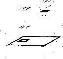
The position of terminal that has the card of outside terminal is determined by ISO07816.Fig. 1 represents by the definite magnetic stripe zone of ISO07816 specification, embossed area, reaches the outside terminal zone.On compound IC-card, the IC module is contained in the outside terminal zone, and the oblique line of Fig. 1 is partly represented the installation prohibited area of the antenna of noncontact coupling usefulness.
Regulation according to ISO7816, be shaped as long limit 85.47 ~ 85.72mm in profile, in the zone of minor face 53.29 ~ 54.03mm, begin to form in the 15.82mm zone magnetic stripe zone from the top, begin 24mm, begin 6.0mm from the left side, begin from the right to form embossed area in the zone of 8.0mm from bottom, begin 28.55mm from the top, begin from the left side to form outside terminal in the zone of 19.87mm.
As the compound IC-card that can be applicable to magnetic stripe and embossing in the prior art, for example have the spy and open disclosed technology in the flat 7-239922 communique.
According to this communique, IC-card constitutes with the support of IC module by IC chip, conveyer and support IC chip and conveyer, wherein, this conveyer with external unit that the IC chip is electrically connected between carry out the transmission of information and/or electric power, and have the contact-type conveyer that a plurality of terminal electrodes of non-contact type conveyer that is made of coil or antenna and the conductive patternization that will be located at the support surface constitute.To have the function modoularization of contact-type and non-contact type dual mode like this, above-mentioned compound IC module embedding is fixed on the plastic clip (plastic card), can the formation of magnetic stripe and embossing not impacted.
This communique also discloses: as mounting means, the antenna or the coil that will be used for the noncontact transmission are arranged to surrounding around the terminal electrode, and be perhaps opposite with above-mentioned form, and antenna is plied in the centre, and terminal electrode is set around it.
That is, be housed in the IC module, can not need being connected aerial coil and IC module of finishing operation by the antenna that non-contact transmission is used.
But for the method that aerial coil is set around terminal electrode, if with reference to specification shown in Figure 1, then it implements very difficult as can be known.That is, in the method that non-contact transmission is housed in antenna in the IC module, can not obtain sufficient antenna area, can only allow communication distance below several millimeters is being so-called closely-coupled mode.
Because the interval maximum of terminal electrode and embossed area has only 1.45mm, thereby antenna and coil are overlapped with terminal electrode on same,, be infeasible from reality so that surround the configuration mode on every side of terminal electrode.Its reason is, aerial coil is being configured under the situation on every side of outside terminal, the maximum outside diameter of coil and minimum diameter are respectively φ 12mm and φ 9.3mm, when forming aerial coil by impressing pattern (print pattern) in this zone, when pattern amplitude and interval are respectively 0.15mm and 0.1mm, then the number of turn and inductance are about 4 circles respectively, 0.4 μ H and 6 circles, 1.0 μ H (the μ H here is expressed as microhenry), therefore, for guaranteeing embossed area, when the periphery of terminal electrode disposes coil, promptly enable to form printed coil, also can only obtain the number circle, and the area of coil can only be very little, can't receive enough electric power, can only allow communication distance in the close-coupled below several millimeters.
The effect of the noncontact transmitting function that is had like this, seldom., can communicate by the antenna that card is passed the exterior read-write device producing to surpassing in 100 millimeters the communication distance in the effect of the noncontact transmitting function of being added on the contact-type conveyer in this zone from tens of millimeters.For this reason, the area of coil is increased, or the number of turn is increased.
Therefore, in the IC module, coil configuration when the periphery of terminal electrode, is promptly enabled to form printed coil, also can only obtain the number circles, and the area of coil can only be very little, can't receive enough electric power.In addition, when producing the number of turn that reaches practical, can touch the pressure embossed area with conductive pattern.
On the other hand,,, be certain to invade embossed area, will be very different with the specification ISO7816 of the IC-card that has outside terminal, thereby be difficult to be received by market when when around the antenna terminal electrode being set as the latter's mounting means.
In addition, compound integrated circuit is with faintness wave work, requires very high to the electric power transmission efficiency.Corresponding therewith prior art for example has the spy to open flat 2-7838 number, spy and opens clear 63-224635 number.But, in this existing example in order to improve the mode of electric power transmission efficiency, only be conceived to the electric power of transmitting electricity, only effective so that can send the situation of more electric power to the electrical efficiency that improves the transmission of electricity side.For this reason, under to the conditional situation of the intensity of radiation field, this mode to the electric power receiving efficiency of receiver side to improve effect little.Be arranged in the compound IC-card in light current magnetic field, can absorb the devices that are radiated the energy in the card more in order to improve this card self because of having the ability that the non-contact type function can receive electric power, must to be provided with.
And, because compound IC-card is built-in with SIC (semiconductor integrated circuit),, preferably obtain more electric current by low electric power in order to reduce the load of power circuit.That is, preferably making the electric power receiver side is Low ESR.But existing technology only is conceived to transmission voltage, and the content relevant with the electric power receiver side is then without any open.
The 1st purpose of the present invention is in order to solve problems of the prior art, a kind of compound IC module is provided and comprises the compound IC-card of this module, even needn't connect with distribution between the antenna that compound IC module and non-contact transmission are used, also can have the receiving sensitivity that can obtain sufficient communication distance, and can make contact-type and two kinds of conveyers of non-contact type keep practical operating state.
The 2nd purpose of the present invention provides a kind of compound IC-card and compound IC module thereof, have two kinds of functions of contact-type and non-contact type, and at least a compound IC-card in transmitting with the reception that the noncontact mode is carried out the reception supply of electric power or signal, the coil of electric power transmitter side (read-write (リ one ダ ラ イ ) side) and the antenna of electric power receiver side (compound IC-card side) are by using the separated coupling mechanism in clearance, the receiving efficiency of transmission ripple is improved in compound IC-card side, improve the electrical efficiency transmission efficiency of signal (or improve) of electric power receiver side, carry out impedance conversion.
The 3rd purpose of the present invention provides a kind of compound IC module and compound IC-card, even for having contact-type conveyer and non-contact type conveyer simultaneously, and be formed with the IC-card of magnetic stripe and embossing on the surface of card, also can not influence the formation of magnetic stripe and embossing, improve the electrical efficiency of electric power receiver side, and carry out impedance conversion, can form the card of minimal thickness.
Disclosure of an invention
(1) compound IC-card of the present invention has two kinds of functions of contact-type and non-contact type, comprises IC module and antenna element,
The IC module comprises: be built-in with the IC chip of contact-type transmitting function and non-contact type transmitting function and be formed with the outside terminal of contact-type conveying element and the module substrate of the 1st pickup coil;
Antenna element comprises: antenna, and the transmission of carrying out the reception supply of electric power at least or signal between the exterior read-write device any in receiving; The 2nd pickup coil is connected with above-mentioned antenna;
The 2nd pickup coil that the 1st pickup coil of IC module and noncontact transmit the antenna element of usefulness is provided with to close-coupled mutually, and IC module and antenna element are by mutual inductance coupling coupling non-contactly.
(2) compound IC-card of the present invention, in (1) described compound IC-card, antenna element comprises capacitive element.
(3) compound IC-card of the present invention in (1) or (2) described compound IC-card, also has embossed area,
The IC module is located at the substantial middle position of a minor face of card, and embossed area is provided with along a long limit of card;
The antenna that noncontact transmits usefulness is arranged on the outside terminal zone of not interfering above-mentioned IC module and any the position in the embossed area.
(4) compound IC-card of the present invention in the compound IC-card of record, also has embossed area in (1) or (2),
The IC module is located at the substantial middle position of a minor face of card, and embossed area is provided with along a long limit of card;
The antenna that noncontact transmits usefulness is arranged on by the following part area surrounded, that is: by the border of the card private side in the outside terminal zone of the border of the card private side of the long limit relative, above-mentioned embossed area, IC module with the long limit that above-mentioned embossed area is set, with the relative minor face institute area surrounded of minor face of the above-mentioned IC module of card is set, and do not interfere the outside terminal zone of above-mentioned IC module and any in the above-mentioned embossed area.
(5) compound IC-card of the present invention, in (1) or (2) described compound IC-card, it also has embossed area;
The IC module is located at the substantial middle position of a minor face of card; Embossed area is provided with along a long limit of card;
At least a portion that noncontact transmits the antenna of usefulness is arranged between the edge of embossed area and card, and between the edge of the outside terminal of above-mentioned IC module zone and card, and be located at periphery, do not interfere the outside terminal zone of above-mentioned IC module and any the position in the above-mentioned embossed area along card.
(6) compound IC-card of the present invention, in (1) or (2) described compound IC-card, it also has magnetic stripe zone and embossed area;
The IC module is located at the substantial middle position of a minor face of card; Embossed area is provided with along a long limit of card; Another long limit along card is provided with above-mentioned magnetic stripe zone,
The antenna of noncontact transmission usefulness is configured to not interfere any in the outside terminal zone of above-mentioned IC module, above-mentioned embossed area and the above-mentioned magnetic stripe zone.
(7) compound IC-card of the present invention, in (1) or (2) described compound IC-card, it also has magnetic stripe zone and embossed area,
The IC module is located at the substantial middle position of a minor face of card, and embossed area is provided with along a long limit of card; The magnetic stripe zone is provided with along another long limit of card,
The antenna that noncontact transmits usefulness roughly along the border of the card private side in magnetic stripe zone, the border of the card outer circumferential side in the outside terminal zone of the border of the outer circumferential side of the card of embossed area, IC module and being provided with, and do not interfere any of outside terminal zone, embossed area and magnetic stripe zone of IC module.
(8) compound IC-card of the present invention, in (1) or (2) described compound IC-card, it also has magnetic stripe zone and embossed area;
The IC module is located at the substantial middle position of a minor face of card; Embossed area is provided with along a long limit of card; The magnetic stripe zone is provided with along another long limit of card;
The antenna that noncontact transmits usefulness is arranged on by the following part area surrounded, that is: by the border of the card private side in the border of the card private side in the outside terminal zone of the border of the card private side of embossed area, IC module, magnetic stripe zone, the minor face institute area surrounded relative, and do not interfere in outside terminal zone, embossed area and the magnetic stripe zone of IC module any with the minor face that the IC module is set.
(9) compound IC-card of the present invention, in (1) or (2) described compound IC-card, antenna element is arranged on the 2nd pickup coil in the outside of the ring of antenna.
(10) compound IC module of the present invention comprises: be built-in with the IC chip of non-contact type propagation function and contact-type transmitting function and be formed with the 1st pickup coil and as the module substrate of the outside terminal of contact-type conveying element;
The 1st pickup coil is arranged on the opposition side that side is set of the outside terminal of module substrate, and the 1st pickup coil adopts the winding coil that will have the Wire-wound of insulating protective film and form.
(11) IC module of the present invention, in (10) described compound IC module, winding coil is wound into spiral fashion and forms around the above-mentioned at least IC chip or near it.
(12) IC module of the present invention, in (10) described compound IC module, winding coil around the IC chip or near it, is wound into ring-type and forms at least.
(13) IC module of the present invention, in (10) described compound IC module, winding coil is reeled and is formed at the end face of the outer circumferential side of module substrate.
(14) IC module of the present invention, in each described compound IC module of (10) to (13), in the installed surface side of the IC of IC module chip, IC chip and the 1st pickup coil are all by resin-sealed.
(15) IC module of the present invention, in each described compound IC module of (10) to (13), the size of module substrate roughly with the equal and opposite in direction in the zone of outside terminal.
(16) compound IC module of the present invention comprises: be built-in with the IC chip of contact-type transmitting function and non-contact type transmitting function and be formed with the 1st pickup coil and the module substrate of the outside terminal of contact-type conveying element;
The opposition side that the 1st pickup coil is provided with side at the outside terminal of above-mentioned module substrate form patterning conductor, be arranged at least the IC chip around or near it in any.
(17) IC module of the present invention, in (16) described compound IC module, winding coil is wound at least one shape in spiral fashion or the ring-type and forms around the encapsulant of IC chip.
(18) IC module of the present invention, in (16) described compound IC module, in the installed surface side of the IC of IC module chip, IC chip and the 1st pickup coil are all by resin-sealed.
(19) IC module of the present invention, in (16) described compound IC module, make peace greatly zone big or small identical of outside terminal of the size of module substrate.
Brief description of drawings
Fig. 1 is the dimensional drawing of the card that has outside terminal of ISO7816 regulation;
Fig. 2 is the equivalent circuit diagram of noncontact coupled circuit that is used to illustrate the principle of noncontact conveyer of the present invention;
Fig. 3 A, Fig. 3 B are the exploded perspective view and the sectional views of structure of the 1st embodiment of expression compound IC-card of the present invention;
Fig. 4 is the synoptic diagram of the 1st example of configuration of the aerial coil of the 1st embodiment;
Fig. 5 is the synoptic diagram of the 2nd example of configuration of the aerial coil of the 1st embodiment;
Fig. 6 is the synoptic diagram of the 3rd example of configuration of the aerial coil of the 1st embodiment;
Fig. 7 is the 4th the synoptic diagram of configuration of the aerial coil of the 1st embodiment;
Fig. 8 A, Fig. 8 B are the exploded perspective view and the sectional views of structure of the 2nd embodiment of expression compound IC-card of the present invention;
Fig. 9 is the synoptic diagram of the 1st example of configuration of the aerial coil of the 2nd embodiment;
Figure 10 is the synoptic diagram of the 2nd example of configuration of the aerial coil of the 2nd embodiment;
Figure 11 is the synoptic diagram of the 3rd example of configuration of the aerial coil of the 2nd embodiment;
Figure 12 A, Figure 12 B are the exploded perspective view and the sectional views of structure of the 3rd embodiment of expression compound IC-card of the present invention;
Figure 13 is the synoptic diagram of the 1st example of configuration of the aerial coil of the 3rd embodiment;
Figure 14 is the synoptic diagram of the 2nd example of configuration of the aerial coil of the 3rd embodiment;
Figure 15 A, Figure 15 B are the synoptic diagram of the 3rd example of configuration of the aerial coil of the 3rd embodiment;
Figure 16 A, Figure 16 B are the synoptic diagram of the 1st example of the structure of capacitive element of the present invention;
Figure 17 A, Figure 17 B are the synoptic diagram of the 2nd example of the structure of capacitive element of the present invention;
Figure 18 A, Figure 18 B are the synoptic diagram of the 3rd example of the structure of capacitive element of the present invention.
Following embodiment with reference to description of drawings compound IC-card of the present invention.
The structure and the ultimate principle of noncontact conveyer at first are described.
Fig. 2 is the equivalent circuit diagram of noncontact coupled circuit that is used to illustrate the principle of noncontact conveyer of the present invention.The transmitter/receiver circuit 101 of the exterior read-write device 100 of non-contact type is connected with transmission receiving coil 102, and this transmission receiving coil is to the supply capability of the noncontact conveyer of compound IC-card 1 and the electromagnetic coupler that carries out message exchange.
On the other hand, the noncontact conveyer of compound IC-card 1 is by constituting with the lower part, that is: the aerial coil 4 that receives with the transmission of the transmission/reception antennas 102 direct electromagnetic coupled of exterior read-write device 100, the reception that participates in electric power and information; Be connected with the two ends of aerial coil 4, constitute the capacitive element 15 in parallel resonance loop; Be installed in the compound IC chip 6 of compound IC module 2; The 1st pickup coil 8 that is connected with compound IC chip 6; The 2nd pickup coil 3 for signal that aerial coil is received transmits and by the configuration of close-coupled ground to the 1st pickup coil with maximal efficiency, is connected with the two ends of the capacitive element 15 of tank circuit.
Here, capacitive element 15 and aerial coil 4 be for being connected in parallel, but also can and aerial coil 4 and the 2nd pickup coil 3 between be connected in series.And, in order to increase the capacity between circuit, can omit capacitive element 15.
Below explanation is from the coupling of exterior read-write device 100 each coil under the situation of compound IC-card 1 transferring electric power and information.
The not shown high-frequency signal that transmitter/receiver circuit 101 by exterior read-write device 100 produces induces high frequency magnetic field sending receiving coil 102.This high-frequency signal as magnetic energy to space radiation.
At this moment, when compound IC-card 1 was arranged in this high frequency magnetic field, the high frequency magnetic field that the transmission receiving coil 102 by exterior read-write device 100 is produced produced electric current in the tank circuit that aerial coil 4 and capacitive element 15 by compound IC-card 1 constitute.At this moment, with compound IC chip 6 direct-connected the 1st pickup coils 8, aerial coil 4, and be connected with the resonance circuit of capacitive element 15, in the 2nd pickup coil 3 of the 1st pickup coil 8 transferring electric powers, all produce induction current, but lack an order of magnitude owing to comparing, so receiving sensitivity depends on the characteristic of aerial coil 4 to a great extent with the quantity of induction in aerial coil 4.
The signal that the resonance circuit of aerial coil 4 and capacitive element 15 receives is transmitted to the 2nd pickup coil 3.Because 2nd pickup coil 3 and 1st pickup coil 8 in the close-coupled mode that produce maximum transmission efficiency dispose, by the mutual inductance coupling of 2nd pickup coil 3 and 1st pickup coil 8, to compound IC chip 6 transmit signal thereafter.The maximum transmission efficiency of the mutual inductance coupling of the 2nd pickup coil 3 and the 1st pickup coil 8 is decided by the selection of network constant.
By the above, receiving feature is improved.Its result decides receiving sensitivity by the characteristic of aerial coil 4, and the area of aerial coil 4 is big more then favourable more.
According to the mode difference of the noncontact conveyer of electromagnetic coupled or electromagnetic induction etc., antenna performance is also different, the example of the characteristic of the induction aerial coil of short-wave band such as table 1 and calculate.
Table 1
| Example | Area coil (long limit * minor face) | | |
| Inductance | |||
| 5 | Inductance | 20 μ H | |
| Ex.1 | 84mm×53mm | 4 | 10 circles |
| Ex.2 | 84mm×37mm | 5 | 11 circles |
| Ex.3 | 64mm×28mm | 6 circles | 14 circles |
| Ex.4 | 64mm×13mm | 7 | 16 circles |
| Ex.5 | 12mm× | 15 circle * 1 | 30 circles |
Here the width that has only * 1 its coil, amplitude are 0.05mm, and the width of remaining situation lower coil, amplitude all are 0.15mm.
Relevant therewith, the inductance of the aerial coil of the RF-ID card of the short-wave band of practicability is about 5 microhenrys now.Such aerial coil can be configured in impressing pattern (printed coil) peripheral part of card.
Refer again to Fig. 1, the stenosis in the gap of the periphery of embossed area and card is arranged in the bottom of the card of Fig. 1, and its value is 2.41mm.If begin to make spiral winding at edge 1mm, and make pattern amplitude and its be spaced apart 0.15mm to the position at center from card, then the number of turn of coil can be configured to 5, when making pattern amplitude and its be spaced apart 0.1mm, then the number of turn of coil can be configured to 7.
If the spy who illustrates in prior art opens in flat 7-239922 number the example, aerial coil is set around the outside terminal of IC module, in the 1.45mm amplitude that specification allows, coil is set, in order to obtain the inductance of 5 microhenrys, need the number of turn 15, therefore the pattern amplitude all must can not realize below 0.05mm.
On the other hand, the number of turn of the aerial coil of the electromagnetic coupled mode of low frequency need surpass the above-mentioned number of turn 7.
For example, consider to need the structure of aerial coil of the inductance of 20 microhenrys.Can realize 10 to 30 the number of turn this moment as can be known according to area coil shown in the table 1.
The coil that surpasses 8 circles can be realized by the winding coil of three-dimensional shape and the printed coil of flat shape.For winding coil, can be configured in the periphery of card by overlapping coiling.For printed coil, generally be on a face, not overlap to form winding.Therefore, when the number of turn is a lot,, should not be configured in the periphery of card in order not touch embossed area.
At this moment, aerial coil is disposed in the following manner: do not comprise magnetic stripe, embossing, outside terminal etc. in the inside of aerial coil prohibited area is installed, this configuration mode can make to be made simply, guarantees reliability, and can make card with low cost.
The 1st embodiment
Fig. 3 A, Fig. 3 B are the brief configuration figure of the compound IC-card of the 1st embodiment of the present invention.Fig. 3 A represents whole structure, and Fig. 3 B is a sectional view of cutting the installation portion of IC module open.
The compound IC module 1 of present embodiment is to be made of the card substrate 10 after antenna substrate 5 usefulness are resin-sealed, the 2nd pickup coil 3 and aerial coil 4 that this antenna substrate has IC module 2, forms with printed coil on the surface of the resin of sheet.
The 1st pickup coil 8 and aerial coil 4 also can form without printed coil, and form with the Wire-wound that has covered insulator.Compound IC chip 6 is contained on the formation face of the 1st pickup coil 8 of module substrate 9, and the terminal electrode 7 of compound IC chip 6 and module substrate 9 is connected by through hole (through hole).
The circuit pattern of compound IC chip 6 and the 1st pickup coil 8 is by wire-bonded (wirebonder), forms circuit, its connection be by with scolding tin and conductive adhesive with the circuit formation face of IC chip with substrate heat is deposited realizes.
The compound IC-card 1 of present embodiment is roughly made as follows.
At first prepare pliability antenna substrate 5, this antenna substrate forms the 2nd pickup coil 3, aerial coil 4 and capacitive element 15 with printed coil on resin substrate.The Wire-wound that the 2nd pickup coil 3 and aerial coil 4 also can cover insulated body and forming.As the resin of antenna substrate 5, use be Polyvinylchloride, also can use polycarbonate, polyimide, PET etc., material is not limited to a kind of.
Then, with antenna substrate 5 sealings, be made into card substrate 10 by injection moulding.When moulding, the position configuration of the 2nd pickup coil 3 is become to overlap with the installation site of compound IC module 2.When making card substrate 10, form the embedded hole 11 of compound IC module 2 by injection moulding.
At last, at the embedded hole 11 of the compound IC module 2 of card substrate 10 that compound IC module 2 is bonding, thus finish compound IC-card 1.As the material of substrate of card, use be vinyl chloride, but other as polycarbonate etc. so long as have the material that cards such as full intensity and embossing can utilize, then all can be used for the present invention.
What draw in Fig. 3 A is that separate with the back side on the surface of card substrate 10, but they were one originally, in the drawings, and the expression like this for the relation of the pickup coil of saying clearly the antenna substrate 5 that in card substrate, seals and embedded hole 11.
In the present embodiment, utilized injection moulding to make card, but so long as can keep the embossing characteristic, then method whatsoever all can be used for the present invention, for example available stacked system, bonding agent filling method.In addition, present embodiment is included in also that the embedded hole 11 to the IC module carries out rag processing after the card moulding.
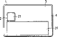
Example 1 is installed
Fig. 4 is the planimetric map of the 1st embodiment with compound IC-card 1 of embossed area, and expression aerial coil 4 is in the installation site of compound IC-card 1 inside.Aerial coil 4 is configured in one piece around card.Embossed area 20 and outside terminal zone 21 are configured in the inside of the circle (loop) of aerial coil 4.The specification of this coil and the E of table 1
X.1 corresponding.
The example of Fig. 4 is less in the number of turn of aerial coil 4, be 3 to 7 o'clock effective, more effective is to be 4 or 5 o'clock.For the antenna substrate 5 of present embodiment, will cut away with the resin plate of embossed area counterpart.This is in order not influence the embossing characteristic.
In Fig. 4 to Fig. 7, dot the profile of antenna substrate 5.
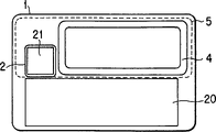
Example 2 is installed
Fig. 5 is the planimetric map of another kind of compound IC-card 1 with the 1st embodiment of embossed area, and expression is configured in embossed area 20 and outside terminal zone 21 general shape of aerial coil 4 of the outside (not being configured in inside) of aerial coil 4.The coil specification of this moment is corresponding to the E of table 1
X.3.The example of Fig. 5 is 10 effective when above in the number of turn of aerial coil 4.
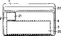
Example 3 is installed
Fig. 6 be have simultaneously magnetic stripe and embossed area the 1st embodiment compound IC-card 1 the 3rd the planimetric map of example is installed, be illustrated in the installation site of the aerial coil 4 of compound IC-card 1 inside.In order to make aerial coil 4 not touch magnetic stripe zone 22, the part beyond the part of the aerial coil relative with the magnetic stripe zone is along the periphery configuration of compound IC-card 1.The specification of the coil of this moment and the E of table 1
X.2 corresponding.In this installation example, the resin plate of the part that antenna substrate 5 also will be corresponding with embossed area 20 cuts away.This is in order not influence the embossing characteristic.
Example 4 is installed
Fig. 7 be have simultaneously magnetic stripe and embossed area the 1st embodiment compound IC-card 1 the 4th the planimetric map of example is installed, expression is not configured in embossed area 20 and magnetic stripe zone 22 general shape of aerial coil of the inside of aerial coil 4.The specification of the coil of this moment and the E of table 1
X.4 corresponding.
The compound IC-card of the 1st embodiment has with the contact-type that has outside terminal and two kinds of corresponding functions of mode of non-contact type of the noncontact coupling element of aerial coil etc. is arranged, by mutual inductance coupling circuit element being set, can noting be used between IC module and aerial coil and to carry out reception supply that the ground connection that is electrically connected carries out electric power and the transmission of signal receives in IC module and aerial coil.
According to this structure, increase as far as possible in the scope of permission by area, and pass the antenna of exterior read-write device with noncontact transmitting function with aerial coil, can keep the sensitivity that can communicate.
By the sensitivity that the signal that increases card receives, can realize the increase of communication distance and/or the transmission output quantity of minimizing exterior read-write device.This exports under the conditional situation transmitting in the electric wave method, and is especially suitable.
And, owing to do not need being connected of IC module and the antenna loop that is built in card substrate, can utilize the existing IC-card manufacturing process that the IC module is bonded in the embedded hole on the card substrate, even on card, apply mechanical stresses such as bending stress, because IC module and antenna loop do not have tie point, the danger that produces fault is very little.
Owing to will be configured to outside terminal zone with the non-aerial coil that directly contacts of exterior read-write device as the electrode of contact-type, and the fitting portion of IC module is not contacted with embossed area and/or magnetic stripe zone, therefore use existing card also can adapt to, have versatility.
And owing to adopt injection moulding, and the material of flexible base plate is in the scope corresponding with embossed area, and therefore a plurality of laminatings being lumped together does not influence embossing yet.
Because the antenna substrate that will comprise aerial coil as flexible printed circuit, makes coil form flat shape, therefore can obtain the card that fully satisfies the ISO7816 specification that thickness is 0.76mm.
As can be seen from Figure 2, make the number of turn of the 1st pickup coil 8 increase the coupling coefficient increase that can make, thereby the energy that transmits to compound IC chip 6 is bigger with the 2nd pickup coil 3.But to the manufacturing technology of present printed circuit board (PCB), the boundary of pattern fabric width is 0.1mm, and for printed coil, it is very difficult making the tens of circles of the interior generation of module basal plane of IC-card.Owing to the progress of head technology, can form coil with the lead that is added with insulating protective film, and can reach tens of microns sizes on the other hand.According to this technology, in the present embodiment, also can form the pickup coil of compound IC module and antenna with the lead that is added with insulating protective film.
As mentioned above, according to the 1st embodiment, a kind of compound IC-card can be provided, do not need being connected of aerial coil that IC module and non-contact transmission use, has the receiving signal sensitivity that obtains abundant communication distance, by being adapted to the formation of embossing processing and magnetic stripe, make two kinds of conveyers of contact-type and non-contact type can keep practical operating state.
Another embodiment of compound IC-card of the present invention below is described.In the explanation of this embodiment, the part identical with the 1st embodiment represented with same reference number, and omitted its detailed description.
The 2nd embodiment
The equivalent circuit diagram of the noncontact coupling circuit of the 2nd embodiment is also similarly represented with Fig. 2 with the 1st embodiment.
In hollow mutual inductance type coupling shown in Figure 2, make the gap smaller between coil can improve transmission efficiency.Therefore, in the 2nd embodiment, not as the 1st embodiment, the 1st, the 2nd pickup coil to be disposed up and down, but make the embedded hole of the internal diameter of the 2nd pickup coil 3 greater than the compound IC module 2 of not shown card substrate, the 1st pickup coil 8 is configured in the almost same plane of coiling of the 2nd pickup coil 3.At this moment, the inside double as of the 2nd pickup coil 3 is an embedded hole.
This situation is compared below the embedded hole that the 2nd pickup coil 3 is configured in compound IC module 2, does not require the depth accuracy of embedded hole processing, makes the embedded hole process equipment of the IC-card that has outside terminal need not transform and can use.
Fig. 8 A, Fig. 8 B are the brief configuration figure of the compound IC-card of the 2nd embodiment of the present invention.Fig. 8 A represents whole structure, and Fig. 8 B is a drawing in side sectional elevation of cutting the installation portion of IC module open.
The compound IC-card 1 of present embodiment is to be made of the card substrate 10 after antenna substrate 5 usefulness are resin-sealed, the 2nd pickup coil 3 and aerial coil 4 that this antenna substrate has IC module 2 of the present invention, forms with printed coil on the surface of the resin of sheet.
Fig. 8 B represents resin-sealed 16 the situation that on every side form winding coil of the 1st pickup coil 8 at compound IC chip 6.As the preparation that forms the 1st pickup coil 8, to around resin-sealed 16 of the compound IC module 2 of to resin-sealed 16 operations till, making with processing such as cutting tools, making coiling become easy.By not shown up-coiler, resin-sealed 16 of compound IC module 2 around directly reel thereafter.
After being wound up into the given number of turn, remove the insulating protective film of the splicing ear of the 1st not shown pickup coil 8, be connected with the not shown given circuit pattern of module substrate 9.
At this moment,, carry out resin-sealedly, can omit resin-sealed 16 cut by using the method for reeling easily when the sealing of carrying out resin-sealed 16.In addition, present embodiment also comprises following content: with winding directly be not wound up into compound IC chip 6 around, utilize the coil up-coiler, make planar coil with other operation, be bonded on the module substrate 9, as the 1st pickup coil 8, thereafter, form resin-sealed 16, so that IC chip 6 and the 1st pickup coil 8 are covered.
In the present embodiment, the section shape that makes the coil of making is the rectangle of fillet, also can be circular, and is unqualified to shape.
The compound IC-card 1 of present embodiment is roughly made as follows.
At first, shown in Fig. 8 A, 8B, prepare pliability antenna substrate 5, this antenna substrate is to form the 2nd pickup coil 3, aerial coil 4 and capacitive element 15 with printed coil in each different zone on resin substrate.
Shown in Fig. 8 B, the 2nd pickup coil 3 of antenna substrate 5 forms in the outside of the embedded hole 11 of compound IC module 2, is finally roughly becoming conplane position configuration to become nested shape with the 1st coil 8 that is installed in compound IC module 2.Here, the 2nd pickup coil 3 and aerial coil 4 also can be by forming with the Wire-wound that insulator covers.
As the resin of antenna substrate 5, use vinyl chloride, also can use polycarbonate, PET, polyimide etc., material is not limited to a kind of.And the thickness of the base material of antenna substrate 5 is the scope from 50 μ m to 300 μ m.Better be about 100 μ m.
Then, with antenna substrate 5 sealings, make card substrate 10 moulding by injection moulding.When moulding, the position configuration of the 2nd pickup coil 3 is become to overlap with the installation site of compound IC module 2.After making card substrate 10, form the embedded hole 11 of compound IC module 2 through injection moulding.
At last, at the embedded hole 11 of the compound IC module 2 of card substrate 10 that compound IC module 2 is bonding, thus finish compound IC-card 1.As the material of card substrate 10, use be vinyl chloride, as long as but other as the material that polycarbonate etc. has the characteristic that can be blocked fully, all can be used for the present invention.What draw in Fig. 8 A is that separate with the back side on the surface of card substrate 10, but they were one originally, in Fig. 8 A, and the expression like this for the relation of the pickup coil of saying clearly the antenna substrate 5 that in card substrate, seals and embedded hole 11.
In the present embodiment, utilized injection moulding to make card, but so long as can keep the characteristic of card, then method whatsoever all can be used for the present invention, for example available stacked system, bonding agent filling method.The embedded hole 11 of processing IC module when in addition, present embodiment also is included in the card moulding.At this moment, in order to carry out the chimeric of IC module, in advance rag is carried out in the inside of the 2nd pickup coil 3 of formation on antenna substrate 5.
Example 1 is installed
Fig. 9 is near the installation example of coiling the 1st pickup coil 8 compound IC chip 6.In this example, compound IC chip 6 is installed in the position of mind-set one end off-centre from module substrate 9.Will be bonding with module substrate 9 with the 1st pickup coil 8 that up-coiler is made, rather than be bonded on the compound IC module 2 of having finished resin-sealed 16 operation, the not shown connection terminal of the 1st pickup coil 8 carries out terminal with the not shown given circuit pattern of module substrate 9 and is connected, and finishes compound IC module 2.Saved like this for the installation of the 1st coil 8 operation of processing around the resin-sealed portion.The section shape of the 1st coil 8 is the rectangle of fillet, also can be circle or ellipse, to shape without limits.
Example 2 is installed
Figure 10 is configured in the 1st pickup coil 8 near the compound IC chip 6, the installation example that forms with the impressing pattern of conductor on the installed surface of the compound IC chip 6 of module substrate 9.
Because the compound IC chip 6 at the outside terminal on the surface of module substrate 9 and the back side be connected pattern and form simultaneously, therefore can simplify being connected of module substrate 9 and the 1st coil 8.In the present embodiment, the section shape of the 1st pickup coil 8 is rectangles of fillet, also can be circle or ellipse, to shape without limits.For example, as shown in figure 11, the 1st pickup coil 8 is wound into annular around resin-sealed 16 of the IC chip, the direction of pointing to induction field is broadened, coupling is strengthened.
The compound IC-card of the 2nd embodiment has with the contact-type that has outside terminal and two kinds of corresponding functions of mode of non-contact type of the noncontact coupling element of aerial coil etc. is arranged, by mutual inductance coupling circuit element is set between IC module and aerial coil, can not be used between IC module and aerial coil and be electrically connected, carry out the reception supply of electric power and the transmission of signal and receive.
In this compound IC-card, make noncontact transmit the internal diameter of the 2nd pickup coil of antenna element of usefulness greater than the periphery of the embedded hole of IC module, the 1st pickup coil that is configured in the IC module forms at the back side of module substrate, by the 1st pickup coil and the 2nd pickup coil are almost disposed at grade, the gap is reduced, improve coupling coefficient.
As a result of, the electromagnetic energy that aerial coil can be received transmits to the IC chip with high coupling coefficient mutual inductance coupling.
Therefore, by blocking, can obtain the effect of the sensitivity of further raising communication near near the antenna of exterior read-write device with noncontact transmitting function.
By increasing the sensitivity of the received signal of blocking, can realize the increase of communication distance and/or the transmission output of minimizing exterior read-write device.This in the electric wave method to transmitting under the conditional situation, especially suitable to the noncontact transmitting function.
And the inside double as of the 2nd pickup coil of the antenna element of noncontact transmission usefulness is the embedded hole of IC module.Like this, below the embedded hole that the 2nd pickup coil is configured in compound IC module, compare, the precision that does not need embedded hole processing, the existing IC module embedded hole process equipment that has the IC-card of outside terminal can use, and the antenna loop that does not need to connect the IC module and be built in card substrate, even apply mechanical stresses such as bending stress on card, because IC module and antenna loop do not have tie point, the disrumpent feelings danger of fault that causes that produces connection terminal is very little.
The 2nd pickup coil of the antenna element by noncontact being transmitted usefulness is arranged on outside the ring of antenna, can prevent that aerial coil from touching embossed area.
As mentioned above, according to the 2nd embodiment, can provide a kind of compound IC-card.Do not need to be connected, have the signal receiving sensitivity that obtains abundant communication distance, and can make contact-type and two kinds of conveyers of non-contact type keep practical operating state with the aerial coil that distribution is used IC module and non-contact transmission.
The 3rd embodiment
The equivalent electrical circuit of the noncontact coupled circuit of the 3rd embodiment is also similarly represented with Fig. 2 with the 1st embodiment.
Figure 12 A, Figure 12 B are the brief configuration figure of the compound IC-card of the 3rd embodiment of the present invention.Figure 12 A represents whole structure, and Figure 12 B is a sectional view of cutting the installation portion of IC module open.
The compound IC module 1 of present embodiment is to be made of the card substrate 10 after antenna substrate 5 usefulness are resin-sealed, the 2nd pickup coil 3 and aerial coil 4 that this antenna substrate has IC module 2, formed by printed coil on the surface of the resin of sheet.
This connection also can connect the circuit formation face and the module substrate 9 of compound IC chip 6 by lead-in wire.
The compound IC-card 1 of present embodiment is made substantially by the following method.
At first, prepare pliability antenna substrate 5, this antenna substrate is to form the 2nd pickup coil 3, aerial coil 4 and capacitive element 15 with printed coil on resin substrate.Here, the 2nd pickup coil 3 and aerial coil 4 also can form by the Wire-wound that covers that will insulate.As the resin of antenna substrate 5, use be vinyl chloride, also can use polycarbonate, polyimide, PET etc., material is not limited to a kind of.
Then, with antenna substrate 5 sealings, make card substrate 10 moulding by injection moulding.When moulding, the position of the 2nd pickup coil 3 is overlapped and disposes with the installation site of compound IC module 2.When making card substrate 10, form the embedded hole 11 of compound IC module 2 through injection moulding.At last, at the embedded hole 11 of the compound IC module 2 of card substrate 10 that compound IC module 2 is bonding, thus finish compound IC-card 1.As the material of card substrate, use be Polyvinylchloride, but other as polycarbonate etc. so long as fully be applicable to the material of the characteristic of card, all can be used for the present invention.
What draw in Figure 12 A is that separate with the back side on the surface of card substrate 10, but they were one originally, in the drawings, and the expression like this for the relation of the pickup coil of saying clearly the antenna substrate 5 that is sealed in the card substrate and embedded hole 11.In the present embodiment, utilized injection moulding to make card, but so long as can keep the embossing characteristic, then method whatsoever all can be used for the present invention, for example available stacked system, bonding agent filling method.In addition, present embodiment also is included in and makes that the embedded hole 11 to the IC module carries out rag processing after the card moulding.
Example 1 is installed
Figure 13 represents the installation example with the 1st pickup coil 8 coiling around compound IC chip 6.
As the preparation that forms the 1st pickup coil 8, to around resin-sealed 16 of the compound IC module 2 of to resin-sealed 16 operation till, making with processing such as cutting tools, making coiling become easy.By up-coiler resin-sealed 16 of compound IC module 2 around directly reel thereafter.After being wound up into the given number of turn, remove the insulating protective film of the splicing ear of the 1st not shown pickup coil 8, be connected with the not shown given circuit pattern of module substrate 9.
At this moment, carry out the type that resin-sealed 16 when sealing reel easily, carry out resin-sealedly, can omit resin-sealed 16 cut by use.In addition, can directly around compound IC chip 6, winding not reeled yet, but utilize the coil up-coiler, make planar coil with other operation, bonding with module substrate 9, as the 1st pickup coil 8.
In the present embodiment, the section shape that makes the coil of making is the rectangle of fillet, also can be ellipse or circle, and there is no particular limitation to shape for present embodiment.
As shown in figure 11, also the 1st pickup coil can be wound into annular around resin-sealed 16 of the IC chip.
Example 2 is installed
Figure 14 installs the installation example that is wound up into the 1st pickup coil 8 on the coil former 17 around compound IC chip 6.
The 1st pickup coil 8 is arranged coiling in the not shown groove of coil former 17.The 1st pickup coil 8 that is winding to coil former 17 is bonded between coil former 17 and the module substrate 9.Thereafter, the not shown connection terminal of the 1st pickup coil 8 is connected with the not shown given circuit pattern of module substrate 9.
At this moment, by on coil former 17, being provided for the terminal of connecting coil, can simplify being connected of module substrate 9 and the 1st coil 8.The section shape of the coil former 17 of present embodiment is the rectangle of fillet, but also can be circular as described above or other shape.
Example 3 is installed
Figure 15 A, Figure 15 B are in the reel installation example of the 1st pickup coil 8 of the end face of module substrate 9.
(thickness direction) reels around the module substrate 9 of the compound IC module 2 of fillet, can form the 1st pickup coil 8.Before the installation of compound IC chip 6, carry out the coiling around module substrate 9 earlier.This also can be the carrying out of the production process of compound IC module 2 at last, to the order of operation without limits.
(thickness direction) reels around the module substrate 9 of the compound IC module 2 of fillet, when the thickness that makes module substrate 9 is 0.3mm, even consider the formation of embossing, and can be at the peripheral 1mm fabric width place of spacing module substrate 9 coiling coil.When making winding diameter be 0.1mm, 3 * 10=30 number of turn of can reeling.This is when form reeling with impressing pattern 5 times.
The compound IC-card of the 3rd embodiment has with the contact-type that has outside terminal and two kinds of corresponding functions of mode of non-contact type of the noncontact coupling element of aerial coil etc. is arranged, by mutual inductance coupling circuit element is set between IC module and aerial coil, the compound IC-card that this compound IC module is embedded can not be used between IC module and aerial coil and be electrically connected, and just can carry out the reception supply of electric power and the transmission reception of signal.
The mutual inductance coupling element of IC module is realized with winding coil, perhaps direct coiling around the resin-sealed portion of IC chip, perhaps the planar coil that will make in advance directly is bonded on the module substrate, perhaps coil is wound on the coil former, and this coil former is bonded on the module substrate, perhaps on the end face of module substrate, reel, make module substrate pickup coil the number of turn the permission scope in many as much as possible, in this compound IC-card that compound IC module is embedded, the electromagnetic energy that aerial coil receives transmits to the IC chip with high coupling coefficient mutual inductance coupling.
Therefore, near the antenna that card is reached exterior read-write device, can obtain the effect of the sensitivity of further raising communication with noncontact transmitting function.
By increasing the sensitivity of the received signal of blocking, can realize the increase of communication distance and/or the transmission output quantity of minimizing exterior read-write device.This uses non-contact IC card under the conditional situation of transmission output quantity of (compound IC-card is used) in the electric wave method, and is especially suitable to IC-card.
And, owing to do not need to be connected between IC module and the antenna circuit that is built in card substrate, prior art about the bonding IC-card manufacturing process that is installed in the embedded hole on the card substrate of IC module can be utilized, even applying on the card under the situation of mechanical stress such as bending stress, owing to do not have tie point between IC module and antenna loop, the danger that produces fault is very little.
As mentioned above, according to the 3rd embodiment, can provide a kind of compound IC-card and compound IC module.Do not need to be connected between IC module and aerial coil that non-contact transmission is used, have the signal receiving sensitivity that obtains abundant communication distance, and make contact-type and two kinds of conveyers of non-contact type can keep the operating state of practicality.
The manufacture method of the aerial coil 4 of then explanation formation noncontact conveyer of the present invention and the capacitive element of resonant circuit.When the capacitive element as IC-card adopts chip capacitor (chip condenser), and when on card, applying power such as bending force, chip capacitor self is destroyed easily with the Wiring pattern on the substrate that electronic circuit has been installed, the reliability of IC-card is reduced, and produce the shortcoming that makes the IC-card thickening because of the thickness of chip capacitor.And, produce distortion in order not make coil because use the winding of electric conductor to form coil, it is noted that the problem that is easy to generate in the manufacturing in use.In order to address this problem, in the present invention, form capacitive element with the electric conductor of retaining wedge substrate.
Following with reference to the description of drawings concrete example.
Concrete example 1
Figure 16 A is the sectional view with the same card substrate of Fig. 3 B, Fig. 8 B, Figure 12 B, the equivalent electrical circuit of Figure 16 B presentation graphs 16A.Here, periphery configuration aerial coil 4 along the one side of substrate 5, this aerial coil 4 utilizes the Wiring pattern of conductive material to realize, this aerial coil 4 has only an end to be connected with an end of the 2nd pickup coil 3, and the other end of aerial coil 4 is placed openly.
On the other hand, the other end of the 2nd pickup coil 3 is drawn towards the another side of substrate 5, and is relative with aerial coil 4, is connected with the electric conductor 104 that is made of conductive material on the another side of substrate 5.
Static capacity is by the pattern that forms the conductive material of aerial coil 4 in one side; Form with the electric conductor 104 that constitutes with conductive material at another side, obtain the series electrical capacitive element 15 of the equivalent electrical circuit of Figure 16 B.
Shown in Figure 16 A, if the amplitude Wb of the amplitude Wa of aerial coil 4 and electric conductor 104 will form required static capacity, though they do not need strict equating, the end face 108 of the amplitude Wb of electric conductor 104 should be configured to not exceed the end face 106 of the amplitude Wa of aerial coil 4 at least.This is the minimizing for the area coil that prevents to be formed by aerial coil 4.
In Figure 16 A, aerial coil 4 is that the number of turn is 2 coil, and the number of turn of aerial coil 4 and pattern amplitude thereof are according to required inductance and static capacity decision.And because the other end of aerial coil 4 can be in the open placement in place arbitrarily, the number of turn can be regulated by the length of the pattern that forms aerial coil 4 at the inductance that the aerial coil more than 14 is had.On the other hand, also can set the relative area of electric conductor 104 and aerial coil 4 arbitrarily, form required static capacity.Therefore, in the present invention, and can only compare with the existing method that its number of turn is regulated its inductance, have the advantage of easy adjusting inductance and static capacity by the area that coil forms.
Concrete example 2
Figure 17 A is the sectional view with the same card substrate of Fig. 3 B, Fig. 8 B, Figure 12 B, the equivalent electrical circuit of Figure 17 B presentation graphs 17A.Here, periphery along the one side of substrate 5 disposes the 2nd aerial coil 4b, the 2nd aerial coil 4b utilizes the Wiring pattern of conductive material to realize, the end of the 2nd aerial coil 4b is connected with an end of the 2nd pickup coil 3, and the other end of the 2nd aerial coil 4b is disposed openly.
On the other hand, the other end of the 2nd pickup coil 3 is drawn towards the another side of substrate 5, relative with the 2nd aerial coil 4b, the end of the 1st aerial coil 4a that forms with Wiring pattern that another side at substrate 5 is made of conductive material is connected, and the other end of the 1st aerial coil 4a is disposed openly.
Static capacity obtains the series electrical capacitive element 15 of the equivalent electrical circuit of Figure 17 B by forming the pattern that conductive material constituted of the 2nd aerial coil 4b in one side and forming the pattern that conductive material constituted of the 1st aerial coil 4a at another side and form.
Shown in Figure 17 A, if the amplitude Wd of the amplitude Wc of the 2nd aerial coil 4b and the 1st aerial coil 4a will form required static capacity, though they do not need strict equating, the end face 118 of the amplitude Wd of at least the 1 aerial coil 4a should be configured to not exceed the end face 116 of the amplitude Wc of the 2nd aerial coil 4b.This is in order to prevent the minimizing of the formed area coil of the 2nd aerial coil 4b.
In Figure 17 A, aerial coil 4a, 4b are that the number of turn is 2 coil, and the number of turn of the 2nd aerial coil 4b and the 1st aerial coil 4a and pattern amplitude thereof are according to required inductance and static capacity decision.And, because the other end of the other end of the 2nd aerial coil 4b and the 1st aerial coil 4a can be placed in place arbitrarily openly, the inductance that the 2nd aerial coil 4b has can be regulated by the length of the pattern that forms the 2nd aerial coil 4b, and the inductance that the 1st aerial coil 4a has can be regulated by the length of the pattern that forms the 1st aerial coil 4a.On the other hand, static capacity increases according to the relative formed area with the 1st aerial coil 4a of the 2nd aerial coil 4b, therefore should have the relative formed area with the 1st aerial coil 4a of the 2nd aerial coil 4b at least.Therefore, in the present invention, and can only compare, have the advantage of easy adjusting inductance and static capacity by the existing method that the formed area of coil and the number of turn are regulated its inductance.
Concrete example 3
Figure 18 A is the sectional view with the same card substrate of Fig. 3 B, Fig. 8 B, Figure 12 B, the equivalent electrical circuit of Figure 18 B presentation graphs 18A.Here, periphery configuration aerial coil 4 along the one side of substrate 5, this aerial coil 4 utilizes the Wiring pattern of conductive material to realize, an end of this aerial coil 4 is connected with an end of the 2nd pickup coil 3, and the other end is connected with the other end of the 2nd pickup coil 3.The electric conductor 124 of configuration, employing conductive material 4 relative on the another side of substrate 5 with aerial coil.
Static capacity is formed by the static capacity between the pattern of the static capacity between the pattern adjacent with aerial coil 4 and electric conductor 124 and aerial coil 4, represents with the series electrical capacitive element 15 of the equivalent electrical circuit of Figure 17 B.
Shown in Figure 18 A, if the amplitude Wf of the amplitude We of aerial coil 4 and electric conductor 124 will form required static capacity, though they do not need strict equating, the end face 128 of the amplitude Wf of electric conductor 124 should be configured to not exceed the end face 126 of the amplitude We of aerial coil 4 at least.This is in order to prevent the minimizing of aerial coil 4 formed area coils.
In Figure 18 A, aerial coil 4 is that the number of turn is 2 coil, and the number of turn of aerial coil 4 and pattern amplitude thereof decide according to required inductance and static capacity.
According to the present invention as above, can realize following compound IC-card, compound IC module.
(1) has the compound IC-card of contact-type and two kinds of functions of non-contact type, comprise IC module and antenna element, the IC module comprises: be built-in with the IC chip of contact-type transmitting function and non-contact type transmitting function and be formed with the outside terminal of contact-type conveying element and the module substrate of the 1st pickup coil; Antenna element comprises: antenna, and the transmission of carrying out the reception supply of electric power at least or signal between the exterior read-write device any in receiving; The 2nd pickup coil is connected with antenna; The 2nd pickup coil that the 1st pickup coil of IC module and noncontact transmit the antenna element of usefulness is provided with to close-coupled mutually, and IC module and antenna element are by mutual inductance coupling coupling non-contactly.
(2) in (1) described compound IC-card, antenna element comprises capacitive element.
(3) in (1) or (2) described compound IC-card, it also has embossed area, and the IC module is located at the substantial middle position of a minor face of card, and embossed area is provided with along a long limit of card; The antenna that noncontact transmits usefulness is arranged on the outside terminal zone of not interfering the IC module and any the position in the embossed area.
(4) in (1) or (2) described compound IC-card, it also has pressure
Mould zone, IC module are located at the substantial middle position of a minor face of card, and above-mentioned embossed area is provided with along a long limit of card; The antenna that noncontact transmits usefulness is arranged on by the following part area surrounded, that is: by the border of the card private side in the outside terminal zone of the border of the card private side of the long limit relative, above-mentioned embossed area, IC module with the long limit that above-mentioned embossed area is set, with the relative minor face institute area surrounded of minor face of the above-mentioned IC module of card is set, and do not interfere the outside terminal zone of IC module and any in the embossed area.
(5) in (1) or (2) described compound IC-card, it also has embossed area; The IC module is located at the substantial middle position of a minor face of card; Embossed area is provided with along a long limit of card; At least a portion that noncontact transmits the antenna of usefulness is arranged on mould
Between the edge of nip territory and card, and between the edge of the outside terminal of IC module zone and card, be located at periphery, do not interfere the outside terminal zone of IC module and any the position in the embossed area along card.
(6) in (1) or (2) described compound IC-card, it also has magnetic
Bar zone and embossed area; The IC module is located at the substantial middle position of a minor face of card; Embossed area is provided with along a long limit of card; Another long limit along card is provided with above-mentioned magnetic stripe zone, and the antenna of noncontact transmission usefulness is configured to not interfere any in the outside terminal zone of above-mentioned IC module, above-mentioned embossed area and the above-mentioned magnetic stripe zone.
(7) in (1) or (2) described compound IC-card, it also has magnetic
Bar zone and embossed area, IC module are located at the substantial middle position of a minor face of card, and embossed area is provided with along a long limit of card; The magnetic stripe zone is provided with along another long limit of card, the antenna that noncontact transmits usefulness roughly along the border of the card private side in magnetic stripe zone, the border of the card outer circumferential side in the outside terminal zone of the border of the outer circumferential side of the card of embossed area, IC module and being provided with, and do not interfere any of outside terminal zone, embossed area and magnetic stripe zone of IC module.
(8) in (1) or (2) described compound IC-card, it also has magnetic
Bar zone and embossed area; The IC module is located at the substantial middle position of a minor face of card; Embossed area is provided with along a long limit of card; The magnetic stripe zone is provided with along another long limit of card; The antenna that noncontact transmits usefulness is arranged on by the following part area surrounded, that is: by the border of the card private side in the border of the card private side in the outside terminal zone of the border of the card private side of embossed area, IC module, magnetic stripe zone, the minor face institute area surrounded relative, and do not interfere in outside terminal zone, embossed area and the magnetic stripe zone of IC module any with the minor face that the IC module is set.
(9) in (1) or (2) described compound IC-card, antenna element will
The 2nd pickup coil is arranged on the outside of the ring of antenna.
(10) in the described compound IC-card of each in (1) to (9),
The 2nd pickup coil almost disposes with nested shape at grade with the 1st pickup coil.
(11) in the described compound IC-card of each in (1) to (9),
The 2nd pickup coil and the 1st pickup coil are almost at grade with supporting state configuration, the inboard profile of the 2nd pickup coil is bigger than the lateral profile of embedded hole of IC module setting in card, and the 1st pickup coil is arranged on the face of the opposition side that side is set of outside terminal of module substrate.
(12) in the described compound IC-card of each in (1) to (9),
The 2nd pickup coil and the 1st pickup coil are almost at grade with supporting state configuration; the 1st pickup coil has the winding coil of the lead that has insulating protective film at least, and this winding coil is reeled around IC chip that the face with the opposition side of the outside terminal of module substrate is provided with.
(13) in the described compound IC-card of each in (1) to (9),
The 2nd pickup coil and the 1st pickup coil are almost at grade with supporting state configuration; the 1st pickup coil has with having the Wire-wound winding coil circlewise of insulating protective film, and the winding coil of this ring-type is reeled around IC chip that the face with the opposition side of the outside terminal of module substrate is provided with.
(14) in the described compound IC-card of each in (1) to (9),
The 2nd pickup coil and the 1st pickup coil are almost at grade with supporting state configuration; the 1st pickup coil has with having the Wire-wound winding coil circlewise of insulating protective film, and the winding coil of this ring-type is coiling near IC chip that the face with the opposition side of the outside terminal of module substrate is provided with.
(15) in the described compound IC-card of each in (1) to (9),
The 2nd pickup coil and the 1st pickup coil be almost at grade with supporting state configuration, and the 1st pickup coil has around the IC chip that the face with the opposition side of the outside terminal of module substrate is provided with or near the coil that forms with conductive pattern it at least.
(16) in the described compound IC-card of each in (1) to (9),
The 1st pickup coil is to adopt the winding coil that the Wire-wound will have insulating protective film constitutes and form.
(17) in the described compound IC-card of each in (1) to (9),
The 1st pickup coil is to adopt the winding coil that the Wire-wound will have insulating protective film constitutes and form, and winding coil being wound into ring-type and disposing around the encapsulant of IC chip.
(18) in the described compound IC-card of each in (1) to (9),
The 1st pickup coil is to adopt the winding coil that the Wire-wound will have insulating protective film constitutes and form, and winding coil is reeled and disposed at the end face of the outer circumferential side of module substrate.
(19) in the described compound IC-card of each in (1) to (18), in the installed surface side of the IC of IC module chip, IC chip and the 1st pickup coil are all by resin-sealed.
(20) in the described compound IC-card of each in (1) to (19), antenna element has the capacitive element that is connected with the 2nd pickup coil with antenna.
(21) in (20) described compound IC-card, capacitive element and antenna, and the 2nd pickup coil be connected in parallel.
(22) in (20) described compound IC-card, capacitive element and antenna, and the 2nd pickup coil be connected in series.
(23) in (20) described compound IC-card, capacitive element is made of conductor layer, and this conductor layer is provided with antenna substrate clampingly on the two sides of antenna substrate.
(24) in (20) described compound IC-card, capacitive element is made of antenna stack and conductor layer, and wherein, antenna stack is arranged on a surface of antenna substrate, conductor layer is arranged on another surface of antenna substrate, with antenna stack with the antenna substrate clamping.
(25) compound IC module of the present invention comprises: be built-in with the IC chip of non-contact type propagation function and contact-type transmitting function and be formed with the 1st pickup coil and the module substrate of the outside terminal of contact-type conveying element; The 1st pickup coil is arranged on the opposition side that side is set of the outside terminal of above-mentioned module substrate, and the 1st pickup coil adopts is will have the Wire-wound of insulating protective film and the winding coil that forms.
(26) in (25) described compound IC module, winding coil is wound into spiral fashion and forms around the above-mentioned at least IC chip or near it.
(27) in (25) described compound IC module, above-mentioned winding coil is wound into ring-type and forms around the above-mentioned at least IC chip or near it.
(28) in (25) described compound IC module, above-mentioned winding coil is reeled and is formed at the end face of the outer circumferential side of above-mentioned module substrate.
(29) in each described compound IC module of (25) to (28), in the installed surface side of the IC of IC module chip, IC chip and the 1st pickup coil are all by resin-sealed.
(30) in each described compound IC module of (25) to (28), the size of module substrate roughly with the equal and opposite in direction in the zone of outside terminal.
(31) compound IC module of the present invention comprises: be built-in with the IC chip of contact-type transmitting function and non-contact type transmitting function and be formed with the 1st pickup coil and the module substrate of the outside terminal of contact-type conveying element; The opposition side that the 1st pickup coil is provided with side at the outside terminal of above-mentioned module substrate form patterning conductor, be arranged on above-mentioned at least IC chip around or near it in any.
(32) in (31) described compound IC module, winding coil is wound at least one shape in spiral fashion or the ring-type and forms around the encapsulant of integrated circuit (IC) chip.
(33) in (31) described compound IC module, in the installed surface side of the IC of integrated circuit modules chip, IC chip and the 1st pickup coil are all by resin-sealed.
(34) in (31) described compound IC module, make peace greatly zone big or small identical of outside terminal of the size of module substrate.
The invention provides a kind of compound IC module and comprise the compound IC-card of this compound IC module, even between the antenna of compound IC module and noncontact transmission usefulness, do not need to connect with distribution, also can have the signal receiving sensitivity that obtains abundant communication distance, and can make contact-type and two kinds of conveyers of non-contact type keep practical operating state.
A kind of compound IC module also is provided and comprises the compound IC-card of this compound IC module, can improve the electrical efficiency transmission efficiency of signal (or improve) of electric power receiver side, and carry out impedance conversion.
A kind of compound IC module also is provided and comprises the compound IC-card of this compound IC module, surface at card is formed with in the IC-card of magnetic stripe and embossing, do not influence the formation of magnetic stripe and embossing, can improve the electrical efficiency of electric power receiver side and carry out impedance conversion, and form the card of minimal thickness.
Claims (19)
1, a kind of compound IC-card has two kinds of functions of contact-type and non-contact type, and it comprises IC module and antenna element, it is characterized in that,
Above-mentioned IC module comprises: be built-in with the IC chip of contact-type transmitting function and non-contact type transmitting function and be formed with as the outside terminal of contact-type conveying element and the module substrate of the 1st pickup coil;
Above-mentioned antenna element comprises: any during the transmission of carrying out the reception supply of electric power at least or signal between antenna, itself and exterior read-write device receives; And the 2nd pickup coil, it is connected with above-mentioned antenna;
The 1st pickup coil of above-mentioned IC module and noncontact transmit the 2nd pickup coil of the antenna element of usefulness, and by close-coupled ground setting mutually, above-mentioned IC module and antenna element are coupled non-contactly by the mutual inductance coupling.
2, compound IC-card according to claim 1 is characterized in that, above-mentioned antenna element has capacitive element.
3, compound IC-card according to claim 1 and 2 is characterized in that, it also has embossed area,
Above-mentioned IC module is located at the substantial middle position of a short brink of card, and above-mentioned embossed area is provided with along a long limit of card;
The antenna that above-mentioned noncontact transmits usefulness is arranged on the outside terminal zone of not interfering above-mentioned IC module and any the position in the above-mentioned embossed area.
4, compound IC-card according to claim 1 and 2 is characterized in that also having: embossed area,
Above-mentioned IC module is located at the substantial middle position of a short brink of card, and above-mentioned embossed area is provided with along a long limit of card;
The antenna that above-mentioned noncontact transmits usefulness is arranged on by the following part area surrounded, with the outside terminal zone of not interfering above-mentioned IC module and any in the above-mentioned embossed area, described area surrounded is: by the border of the card private side in the outside terminal zone of the border of the card private side of the long limit relative with the long limit that above-mentioned embossed area is set, above-mentioned embossed area, IC module, and the relative minor face institute area surrounded of minor face of the above-mentioned IC module of card is set.
5, compound IC-card according to claim 1 and 2 is characterized in that also having: embossed area,
Above-mentioned IC module is located at the substantial middle position of a short brink of card, and above-mentioned embossed area is provided with along a long limit of card,
Above-mentioned noncontact transmits at least a portion of the antenna of usefulness, be arranged between the edge of above-mentioned embossed area and card, and between the edge of the outside terminal of above-mentioned IC module zone and card, be located at periphery, do not interfere the outside terminal zone of above-mentioned IC module and any the position in the above-mentioned embossed area along card.
6, compound IC-card according to claim 1 and 2 is characterized in that also having: magnetic stripe zone and embossed area,
Above-mentioned IC module is located at the substantial middle position of a short brink of card, and above-mentioned embossed area is provided with along a long limit of card, and above-mentioned magnetic stripe zone is provided with along another long limit of card,
The antenna of above-mentioned noncontact transmission usefulness is configured to not interfere any in the outside terminal zone of above-mentioned IC module, above-mentioned embossed area and the above-mentioned magnetic stripe zone.
7, compound IC-card according to claim 1 and 2 is characterized in that also having magnetic stripe zone and embossed area,
Above-mentioned IC module is located at the substantial middle position of a short brink of card, and above-mentioned embossed area is provided with along a long limit of card, and above-mentioned magnetic stripe zone is provided with along another long limit of card,
The antenna that above-mentioned noncontact transmits usefulness roughly is provided with along the border of the card outer circumferential side in the outside terminal zone of the border of the outer circumferential side of the card of the border of the card private side in above-mentioned magnetic stripe zone, above-mentioned embossed area, above-mentioned IC module, and does not interfere the outside terminal zone of above-mentioned IC module, above-mentioned embossed area and above-mentioned magnetic stripe zone any.
8, compound IC-card according to claim 1 and 2 is characterized in that also having magnetic stripe zone and embossed area,
Above-mentioned IC module is located at the substantial middle position of a short brink of card, and above-mentioned embossed area is provided with along a long limit of card, and above-mentioned magnetic stripe zone is provided with along another long limit of card;
The antenna that above-mentioned noncontact transmits usefulness is arranged on by the following part area surrounded, that is: by the border of the card private side in the border of the card private side in the outside terminal zone of the border of the card private side of above-mentioned embossed area, IC module, above-mentioned magnetic stripe zone, the minor face institute area surrounded relative, and do not interfere in the outside terminal zone of above-mentioned IC module, above-mentioned embossed area and the above-mentioned magnetic stripe zone any with the minor face that above-mentioned IC module is set.
9, compound IC-card according to claim 1 and 2 is characterized in that, above-mentioned antenna element is arranged on above-mentioned the 2nd pickup coil in the outside of the ring of above-mentioned antenna.
10, a kind of compound IC module, it is characterized in that, comprise: the IC chip that is built-in with non-contact type transmitting function and contact-type transmitting function be formed with the 1st pickup coil that is connected with antenna and as the module substrate of the outside terminal of contact-type conveying element as the non-contact type conveying element
Above-mentioned the 1st pickup coil is arranged on the opposition side that side is set of the outside terminal of above-mentioned module substrate, and the 1st pickup coil adopts is will have the Wire-wound of insulating protective film and the winding coil that forms.
11, compound IC module according to claim 10 is characterized in that, above-mentioned winding coil is wound into spiral fashion and forms around the above-mentioned at least IC chip or near it.
12, compound IC module according to claim 10 is characterized in that, above-mentioned winding coil is wound into ring-type and forms around the above-mentioned at least IC chip or near it.
13, compound IC module according to claim 10 is characterized in that, above-mentioned winding coil is reeled and formed at the end face of the outer circumferential side of above-mentioned module substrate.
According to each described compound IC module in the claim 10 to 13, it is characterized in that 14, in the installed surface side of the IC of above-mentioned IC module chip, above-mentioned IC chip and above-mentioned the 1st pickup coil are all by resin-sealed.
15, according to each described compound IC module in the claim 10 to 13, it is characterized in that, the size of above-mentioned module substrate roughly with the equal and opposite in direction in the zone of said external terminal.
16, a kind of compound IC module, it is characterized in that, comprising: the module substrate of IC chip that is built-in with contact-type transmitting function and non-contact type transmitting function and the outside terminal that is formed with the 1st pickup coil that is connected with antenna and contact-type conveying element as the non-contact type conveying element;
Above-mentioned the 1st pickup coil is provided with side at the outside terminal of above-mentioned module substrate opposition side forms with the conductor of patterning, and be arranged on above-mentioned at least IC chip around or near it in arbitrary place.
17, compound IC module according to claim 16 is characterized in that, above-mentioned winding coil is wound at least one shape in spiral fashion or the ring-type and forms around the encapsulant of above-mentioned IC chip.
18, compound IC module according to claim 16 is characterized in that, in the installed surface side of the IC of above-mentioned IC module chip, above-mentioned IC chip and above-mentioned the 1st pickup coil are all by resin-sealed.
19, compound IC module according to claim 16 is characterized in that, make peace greatly zone big or small identical of said external terminal of the size of above-mentioned module substrate.
Applications Claiming Priority (6)
| Application Number | Priority Date | Filing Date | Title |
|---|---|---|---|
| JP31394497A JPH11149536A (en) | 1997-11-14 | 1997-11-14 | Composite ic card |
| JP31394697A JP3800766B2 (en) | 1997-11-14 | 1997-11-14 | Compound IC module and compound IC card |
| JP313945/1997 | 1997-11-14 | ||
| JP313944/1997 | 1997-11-14 | ||
| JP31394597A JP3800765B2 (en) | 1997-11-14 | 1997-11-14 | Compound IC card |
| JP313946/1997 | 1997-11-14 |
Publications (2)
| Publication Number | Publication Date |
|---|---|
| CN1278936A CN1278936A (en) | 2001-01-03 |
| CN1179295C true CN1179295C (en) | 2004-12-08 |
Family
ID=27339370
Family Applications (1)
| Application Number | Title | Priority Date | Filing Date |
|---|---|---|---|
| CNB988110938A Expired - Lifetime CN1179295C (en) | 1997-11-14 | 1998-11-16 | Composite IC module and composite IC card |
Country Status (5)
| Country | Link |
|---|---|
| US (1) | US6378774B1 (en) |
| EP (1) | EP1031939B1 (en) |
| CN (1) | CN1179295C (en) |
| DE (1) | DE69831592T2 (en) |
| WO (1) | WO1999026195A1 (en) |
Cited By (1)
| Publication number | Priority date | Publication date | Assignee | Title |
|---|---|---|---|---|
| CN107408221A (en) * | 2015-03-31 | 2017-11-28 | 索尼公司 | Electronic circuit and communicator |
Families Citing this family (348)
| Publication number | Priority date | Publication date | Assignee | Title |
|---|---|---|---|---|
| IL122250A (en) * | 1997-11-19 | 2003-07-31 | On Track Innovations Ltd | Smart card amenable to assembly using two manufacturing stages and a method of manufacture thereof |
| EP0977145A3 (en) * | 1998-07-28 | 2002-11-06 | Kabushiki Kaisha Toshiba | Radio IC card |
| US6837438B1 (en) * | 1998-10-30 | 2005-01-04 | Hitachi Maxell, Ltd. | Non-contact information medium and communication system utilizing the same |
| US6577229B1 (en) * | 1999-06-10 | 2003-06-10 | Cubic Corporation | Multiple protocol smart card communication device |
| DE10006816C2 (en) * | 2000-02-15 | 2003-03-13 | Sokymat Id Component Gmbh | Transponder device for the identification of objects in relation to facilities |
| JP4239352B2 (en) * | 2000-03-28 | 2009-03-18 | 株式会社日立製作所 | Manufacturing method of electronic device |
| FR2811108B1 (en) * | 2000-06-29 | 2002-09-27 | A S K | NON-CONTACT PERIPHERAL DISPLAY DEVICE FOR NON-CONTACT PORTABLE OBJECT |
| DE10032128A1 (en) * | 2000-07-05 | 2002-01-17 | Giesecke & Devrient Gmbh | Security paper and value document made from it |
| US20030169169A1 (en) * | 2000-08-17 | 2003-09-11 | Luc Wuidart | Antenna generating an electromagnetic field for transponder |
| EP1195714A1 (en) * | 2000-10-04 | 2002-04-10 | Sokymat S.A. | Transponder unit |
| US6634564B2 (en) * | 2000-10-24 | 2003-10-21 | Dai Nippon Printing Co., Ltd. | Contact/noncontact type data carrier module |
| US6628240B2 (en) * | 2000-11-08 | 2003-09-30 | American Pacific Technology | Method and apparatus for rapid staking of antennae in smart card manufacture |
| JP3468227B2 (en) * | 2001-04-18 | 2003-11-17 | 株式会社村田製作所 | Switching power supply module |
| JP2002342731A (en) | 2001-05-16 | 2002-11-29 | Matsushita Electric Ind Co Ltd | Composite ic card |
| FI112550B (en) * | 2001-05-31 | 2003-12-15 | Rafsec Oy | Smart label and smart label path |
| JP4257679B2 (en) * | 2001-09-18 | 2009-04-22 | ナグライーデー エスアー | Electronic label and manufacturing method thereof |
| ATE329327T1 (en) * | 2001-11-21 | 2006-06-15 | Mineral Lassen Llc | WIRED INTERFACE TO A WIRELESS COMMUNICATIONS DEVICE |
| EP1315234A1 (en) * | 2001-11-26 | 2003-05-28 | Eta SA Fabriques d'Ebauches | VHF receiving antenna housed in the bracelet of a portable electronic device |
| MXPA04007541A (en) * | 2002-02-04 | 2004-11-10 | Raytheon Co | Enhancement antenna for article identification. |
| US7344074B2 (en) * | 2002-04-08 | 2008-03-18 | Nokia Corporation | Mobile terminal featuring smart card interrupt |
| JP4058300B2 (en) * | 2002-06-21 | 2008-03-05 | 株式会社日立製作所 | Portable information device |
| GB2393076A (en) | 2002-09-12 | 2004-03-17 | Rf Tags Ltd | Radio frequency identification tag which has a ground plane not substantially larger than the area spanned by the patch antenna |
| KR20040038134A (en) * | 2002-10-31 | 2004-05-08 | 주식회사 쓰리비 시스템 | smart card of a combination type providing with a stable contactless communication apparatus |
| DE10258670A1 (en) * | 2002-12-13 | 2004-06-24 | Giesecke & Devrient Gmbh | Transponder for contactless transmission of data has two electrically-isolated oscillator circuits that are driven in common |
| DE10258511A1 (en) * | 2002-12-14 | 2004-07-08 | Infineon Technologies Ag | Integrated circuit and associated packaged integrated circuit |
| JP4241147B2 (en) * | 2003-04-10 | 2009-03-18 | ソニー株式会社 | IC card manufacturing method |
| US20040243267A1 (en) * | 2003-05-30 | 2004-12-02 | Shih-Wen Tu | Systematic control of cross fabrication (fab) engineering changes in integrated circuit (IC) foundry manufacturing |
| US20040242270A1 (en) * | 2003-06-02 | 2004-12-02 | Endicott Interconnect Technologies, Inc. | Electronic card |
| US7013365B2 (en) * | 2003-06-16 | 2006-03-14 | Michael Arnouse | System of secure personal identification, information processing, and precise point of contact location and timing |
| JP4325621B2 (en) * | 2003-08-13 | 2009-09-02 | 株式会社村田製作所 | Reader / writer and mobile communication device |
| JP3982476B2 (en) * | 2003-10-01 | 2007-09-26 | ソニー株式会社 | Communications system |
| US7163155B2 (en) * | 2003-11-05 | 2007-01-16 | Interdigital Technology Corporation | ASIC-embedded switchable antenna arrays |
| DE10356153B4 (en) * | 2003-12-02 | 2010-01-14 | Infineon Technologies Ag | Module for contactless chip cards or identification systems |
| KR20070026346A (en) * | 2003-12-26 | 2007-03-08 | 도레이 엔지니어링 가부시키가이샤 | Electronic circuit board intermediate member, manufacturing method therefor, manufacturing equipment therefor, method for manufacturing noncontact id card and the like, and equipment therefor |
| DE202005021690U1 (en) | 2004-02-04 | 2010-02-04 | Bibliotheca Rfid Library Systems Ag | Resonance etiquette on a disk provided with a metallization |
| DE102004021872B3 (en) * | 2004-05-04 | 2005-12-22 | Infineon Technologies Ag | Chip card, method for producing a chip card and electrically conductive contacting element |
| DE602005027347D1 (en) * | 2004-06-10 | 2011-05-19 | Panasonic Corp | RADIO LABEL AND DISTANCE MODIFICATION METHOD FOR RADIO LABEL COMMUNICATION |
| US7274297B2 (en) * | 2004-07-01 | 2007-09-25 | Intermec Ip Corp. | RFID tag and method of manufacture |
| US20060044769A1 (en) * | 2004-09-01 | 2006-03-02 | Forster Ian J | RFID device with magnetic coupling |
| US7158033B2 (en) * | 2004-09-01 | 2007-01-02 | Avery Dennison Corporation | RFID device with combined reactive coupler |
| JP2006179766A (en) * | 2004-12-24 | 2006-07-06 | Mitsubishi Electric Corp | Power module and its manufacturing method |
| JP4169158B2 (en) * | 2004-12-24 | 2008-10-22 | インターナショナル・ビジネス・マシーンズ・コーポレーション | Wireless IC chip, position recognition system using the same, and security system |
| JP4473141B2 (en) * | 2005-01-04 | 2010-06-02 | 日立オートモティブシステムズ株式会社 | Electronic control unit |
| WO2006107862A2 (en) * | 2005-04-04 | 2006-10-12 | Mastercard International Incorporated | A system and method enabling fourth line embossing on contactless cards |
| WO2006116772A2 (en) * | 2005-04-27 | 2006-11-02 | Privasys, Inc. | Electronic cards and methods for making same |
| US20060244575A1 (en) * | 2005-04-29 | 2006-11-02 | Nick Ramirez | Key-less control apparatus for motor vehicles |
| US8325026B2 (en) * | 2005-04-29 | 2012-12-04 | Heistproof, Llc | Remote ignition, theft deterrence, and records keeping system for a vehicle |
| US8477020B2 (en) | 2005-04-29 | 2013-07-02 | Heistproof, Llc | Remote ignition, theft detterence, and records keeping system for a vehicle |
| US7060611B1 (en) * | 2005-06-10 | 2006-06-13 | Ycl Mechanical Co., Ltd. | Method for manufacturing electric device for signal transmission |
| WO2007012109A1 (en) * | 2005-07-28 | 2007-02-01 | Tagsys Sas | Rfid tag containing two tuned circuits |
| RU2008110177A (en) * | 2005-08-18 | 2009-09-27 | АйВиАй СМАРТ ТЕКНОЛОДЖИЗ, ИНК. (US) | SYSTEM AND METHOD OF BIOMETRIC AUTHENTICATION |
| US20110133896A1 (en) * | 2007-10-17 | 2011-06-09 | Bae Systems Information And Electronic Systems Integration Inc. | Methods For Coupling An RFID Chip To An Antenna |
| FR2890212B1 (en) * | 2005-08-30 | 2009-08-21 | Smart Packaging Solutions Sps | ELECTRONIC MODULE WITH A DOUBLE COMMUNICATION INTERFACE, IN PARTICULAR FOR A CHIP CARD |
| DE102005042444B4 (en) * | 2005-09-06 | 2007-10-11 | Ksw Microtec Ag | Arrangement for an RFID transponder antenna |
| WO2007033706A1 (en) * | 2005-09-24 | 2007-03-29 | Dräger Medical AG & Co. KG | Multipart medical system having a bridging element |
| US8081062B2 (en) * | 2005-09-29 | 2011-12-20 | Electronics And Telecommunications Research Institute | Transmit/receive antenna system having offset feed points for high isolation |
| FR2893162B1 (en) * | 2005-11-08 | 2008-02-15 | Oberthur Card Syst Sa | MICROCIRCUIT CARD COMPRISING A ADVANCED INTERDIGITAL CAPACITOR |
| FR2893163B1 (en) | 2005-11-08 | 2008-02-01 | Oberthur Card Syst Sa | METHOD FOR MANUFACTURING A MICROCIRCUIT CARD AND A MICROCIRCUIT CARD, IN PARTICULAR A MAGNETIC ANTENNA. |
| US7519328B2 (en) | 2006-01-19 | 2009-04-14 | Murata Manufacturing Co., Ltd. | Wireless IC device and component for wireless IC device |
| EP3367500B1 (en) * | 2006-01-19 | 2021-08-11 | Murata Manufacturing Co., Ltd. | Wireless ic device |
| FR2899000B1 (en) * | 2006-03-24 | 2008-10-17 | Arjowiggins Security Soc Par A | RADIOFREQUENCY DEVICE COMPRISING AN ELECTRONIC COMPONENT COMPRISING AN INTEGRATED ANTENNA AND COUPLED ELECTROMAGNETICALLY TO AN AMPLIFICATION ANTENNA |
| US20090173793A1 (en) * | 2006-03-30 | 2009-07-09 | Oji Paper Co., Ltd. | Ic module, ic inlet, and ic mounted body |
| WO2007116829A1 (en) * | 2006-03-31 | 2007-10-18 | Hitachi Chemical Co., Ltd. | Electronic tag |
| JP4998463B2 (en) | 2006-04-10 | 2012-08-15 | 株式会社村田製作所 | Wireless IC device |
| BRPI0702888B1 (en) * | 2006-04-14 | 2019-09-17 | Murata Manufacturing Co., Ltd | ANTENNA |
| CN101346852B (en) | 2006-04-14 | 2012-12-26 | 株式会社村田制作所 | Wireless IC device |
| JP4803253B2 (en) * | 2006-04-26 | 2011-10-26 | 株式会社村田製作所 | Article with power supply circuit board |
| US9064198B2 (en) | 2006-04-26 | 2015-06-23 | Murata Manufacturing Co., Ltd. | Electromagnetic-coupling-module-attached article |
| IL175824A0 (en) * | 2006-05-22 | 2007-09-20 | On Track Innovations Ltd | Data transaction card having a tunable coil antenna with reduced footprint |
| JP4325744B2 (en) | 2006-05-26 | 2009-09-02 | 株式会社村田製作所 | Data combiner |
| CN101454989A (en) * | 2006-05-30 | 2009-06-10 | 株式会社村田制作所 | Information terminal |
| EP2023275B1 (en) * | 2006-06-01 | 2011-04-27 | Murata Manufacturing Co. Ltd. | Radio frequency ic device and composite component for radio frequency ic device |
| JP4983794B2 (en) * | 2006-06-12 | 2012-07-25 | 株式会社村田製作所 | Electromagnetic coupling module, wireless IC device inspection system, electromagnetic coupling module using the same, and method of manufacturing wireless IC device |
| US8674888B2 (en) * | 2006-06-21 | 2014-03-18 | Broadcom Corporation | Integrated circuit with power supply line antenna structure and methods for use therewith |
| EP1870797B2 (en) * | 2006-06-23 | 2020-10-07 | ASTRA Gesellschaft für Asset Management mbH & Co. KG | Textile information carrier |
| CN101467209B (en) | 2006-06-30 | 2012-03-21 | 株式会社村田制作所 | Optical disc |
| JP4957724B2 (en) * | 2006-07-11 | 2012-06-20 | 株式会社村田製作所 | Antenna and wireless IC device |
| US7999383B2 (en) | 2006-07-21 | 2011-08-16 | Bae Systems Information And Electronic Systems Integration Inc. | High speed, high density, low power die interconnect system |
| DE112007001912T5 (en) | 2006-08-24 | 2009-07-30 | Murata Mfg. Co., Ltd., Nagaokakyo-shi | High frequency IC device test system and method of making high frequency IC devices using same |
| FR2893164B1 (en) * | 2006-08-31 | 2012-09-28 | Oberthur Card Syst Sa | METHOD FOR MANUFACTURING A MICRO-CIRCUIT BOARD, IN PARTICULAR A MAGNETIC ANTENNA |
| JP5052079B2 (en) * | 2006-09-08 | 2012-10-17 | 株式会社半導体エネルギー研究所 | Sensor device and containers having the same |
| US20100006655A1 (en) * | 2006-09-08 | 2010-01-14 | Simon Phillips | Sub-card personalization process using temporary antenna |
| WO2008050535A1 (en) | 2006-09-26 | 2008-05-02 | Murata Manufacturing Co., Ltd. | Electromagnetically coupled module and article with electromagnetically coupled module |
| EP2056488B1 (en) * | 2006-10-27 | 2014-09-03 | Murata Manufacturing Co. Ltd. | Article with electromagnetically coupled module |
| DE102006052517A1 (en) * | 2006-11-06 | 2008-05-08 | Bielomatik Leuze Gmbh + Co.Kg | Chip module for an RFID system |
| DE102006062308A1 (en) * | 2006-12-27 | 2008-07-17 | ASTRA Gesellschaft für Asset Management mbH & Co. KG | Passive detection tile |
| JP4835696B2 (en) | 2007-01-26 | 2011-12-14 | 株式会社村田製作所 | Container with electromagnetic coupling module |
| JP4888494B2 (en) | 2007-02-06 | 2012-02-29 | 株式会社村田製作所 | Packaging material with electromagnetic coupling module |
| WO2008096574A1 (en) * | 2007-02-06 | 2008-08-14 | Murata Manufacturing Co., Ltd. | Packing material provided with electromagnetically coupled module |
| FR2915011B1 (en) * | 2007-03-29 | 2009-06-05 | Smart Packaging Solutions Sps | CHIP CARD WITH DOUBLE COMMUNICATION INTERFACE |
| EP2133827B1 (en) | 2007-04-06 | 2012-04-25 | Murata Manufacturing Co. Ltd. | Radio ic device |
| US8009101B2 (en) | 2007-04-06 | 2011-08-30 | Murata Manufacturing Co., Ltd. | Wireless IC device |
| WO2008126649A1 (en) * | 2007-04-09 | 2008-10-23 | Murata Manufacturing Co., Ltd. | Wireless ic device |
| US8235299B2 (en) | 2007-07-04 | 2012-08-07 | Murata Manufacturing Co., Ltd. | Wireless IC device and component for wireless IC device |
| US7762472B2 (en) | 2007-07-04 | 2010-07-27 | Murata Manufacturing Co., Ltd | Wireless IC device |
| FR2915010B1 (en) * | 2007-04-16 | 2009-06-05 | Smart Packaging Solutions Sps | MICROELECTRONIC MODULE WITH A DOUBLE COMMUNICATION INTERFACE, IN PARTICULAR FOR A CHIP CARD. |
| HK1109708A2 (en) * | 2007-04-24 | 2008-06-13 | On Track Innovations Ltd | Interface card and apparatus and process for the formation thereof |
| JP4930586B2 (en) * | 2007-04-26 | 2012-05-16 | 株式会社村田製作所 | Wireless IC device |
| EP2141769A4 (en) | 2007-04-27 | 2010-08-11 | Murata Manufacturing Co | Wireless ic device |
| ATE544129T1 (en) * | 2007-04-27 | 2012-02-15 | Murata Manufacturing Co | WIRELESS IC DEVICE |
| DE112008000065B4 (en) | 2007-05-10 | 2011-07-07 | Murata Manufacturing Co., Ltd., Kyoto-fu | Wireless IC device |
| JP4666102B2 (en) | 2007-05-11 | 2011-04-06 | 株式会社村田製作所 | Wireless IC device |
| DE102007022615A1 (en) * | 2007-05-15 | 2008-11-20 | Infineon Technologies Ag | Contactless transmission system and method of making the same |
| DE102007029083B4 (en) * | 2007-06-21 | 2019-05-16 | ASTRA Gesellschaft für Asset Management mbH & Co. KG | Card carrier with Detektierplättchen |
| JP4396785B2 (en) * | 2007-06-27 | 2010-01-13 | 株式会社村田製作所 | Wireless IC device |
| IL184260A0 (en) * | 2007-06-27 | 2008-03-20 | On Track Innovations Ltd | Mobile telecommunications device having sim/antenna coil interface |
| JP4466795B2 (en) | 2007-07-09 | 2010-05-26 | 株式会社村田製作所 | Wireless IC device |
| CN104540317B (en) | 2007-07-17 | 2018-11-02 | 株式会社村田制作所 | printed wiring substrate |
| EP2086052B1 (en) * | 2007-07-18 | 2012-05-02 | Murata Manufacturing Co. Ltd. | Wireless ic device |
| WO2009011375A1 (en) | 2007-07-18 | 2009-01-22 | Murata Manufacturing Co., Ltd. | Wireless ic device and method for manufacturing the same |
| CN102915462B (en) * | 2007-07-18 | 2017-03-01 | 株式会社村田制作所 | Wireless IC device |
| US20090021352A1 (en) * | 2007-07-18 | 2009-01-22 | Murata Manufacturing Co., Ltd. | Radio frequency ic device and electronic apparatus |
| US7830311B2 (en) | 2007-07-18 | 2010-11-09 | Murata Manufacturing Co., Ltd. | Wireless IC device and electronic device |
| JP5155616B2 (en) * | 2007-07-25 | 2013-03-06 | 沖プリンテッドサーキット株式会社 | RFID tag, RFID system, and RFID tag manufacturing method |
| FR2919409B1 (en) | 2007-07-26 | 2009-09-04 | Smart Packaging Solutions Sps | SECURE DOCUMENT WITH NON-CONTACT CHIP WITH DATA PROTECTION AGAINST UNAUTHORIZED READING. |
| US7973722B1 (en) | 2007-08-28 | 2011-07-05 | Apple Inc. | Electronic device with conductive housing and near field antenna |
| EP2045872B1 (en) * | 2007-10-03 | 2011-08-10 | Assa Abloy Ab | Coupling device for transponder and smart card with such device |
| US8028923B2 (en) * | 2007-11-14 | 2011-10-04 | Smartrac Ip B.V. | Electronic inlay structure and method of manufacture thereof |
| US20090123743A1 (en) * | 2007-11-14 | 2009-05-14 | Guy Shafran | Method of manufacture of wire imbedded inlay |
| JP5403903B2 (en) | 2007-12-04 | 2014-01-29 | ルネサスエレクトロニクス株式会社 | Semiconductor device, manufacturing method thereof, and signal transmission / reception method using the semiconductor device |
| US20090145971A1 (en) * | 2007-12-07 | 2009-06-11 | Wen Cheng Yin | Printed wireless rf identification label structure |
| EP2096709B1 (en) | 2007-12-20 | 2012-04-25 | Murata Manufacturing Co., Ltd. | Radio ic device |
| US20090159699A1 (en) | 2007-12-24 | 2009-06-25 | Dynamics Inc. | Payment cards and devices operable to receive point-of-sale actions before point-of-sale and forward actions at point-of-sale |
| EP2717196B1 (en) * | 2007-12-26 | 2020-05-13 | Murata Manufacturing Co., Ltd. | Antenna device and wireless IC device |
| JP4518211B2 (en) * | 2008-03-03 | 2010-08-04 | 株式会社村田製作所 | Compound antenna |
| EP2251934B1 (en) | 2008-03-03 | 2018-05-02 | Murata Manufacturing Co. Ltd. | Wireless ic device and wireless communication system |
| CN101978383B (en) * | 2008-03-20 | 2016-03-23 | 国泰银恩企业有限责任公司 | For transmission circuit and the NFC device or the RFID read/write device that comprise this transmission circuit of contactless communication |
| WO2009119548A1 (en) * | 2008-03-26 | 2009-10-01 | 株式会社村田製作所 | Radio ic device |
| EP2264831B1 (en) * | 2008-04-14 | 2020-05-27 | Murata Manufacturing Co. Ltd. | Radio ic device, electronic device, and method for adjusting resonance frequency of radio ic device |
| US20110025465A1 (en) * | 2008-04-16 | 2011-02-03 | Ole Danekilde | Wireless information carrier |
| JP4609604B2 (en) | 2008-05-21 | 2011-01-12 | 株式会社村田製作所 | Wireless IC device |
| WO2009142756A2 (en) * | 2008-05-22 | 2009-11-26 | California Institute Of Technology | On-chip highly-efficient antennas using strong resonant coupling |
| WO2009142068A1 (en) * | 2008-05-22 | 2009-11-26 | 株式会社村田製作所 | Wireless ic device and method for manufacturing the same |
| WO2009145007A1 (en) * | 2008-05-26 | 2009-12-03 | 株式会社村田製作所 | Wireless ic device system and method for authenticating wireless ic device |
| CN102047500B (en) * | 2008-05-28 | 2014-05-28 | 株式会社村田制作所 | Wireless ic device and component for a wireless ic device |
| JP4557186B2 (en) | 2008-06-25 | 2010-10-06 | 株式会社村田製作所 | Wireless IC device and manufacturing method thereof |
| EP2306586B1 (en) * | 2008-07-04 | 2014-04-02 | Murata Manufacturing Co. Ltd. | Wireless ic device |
| US9104899B2 (en) * | 2008-08-13 | 2015-08-11 | Infineon Technologies Ag | Multiple transceivers operable as a single transceiver |
| EP2320519B1 (en) * | 2008-08-19 | 2017-04-12 | Murata Manufacturing Co., Ltd. | Wireless ic device and method for manufacturing same |
| US20100090008A1 (en) * | 2008-10-13 | 2010-04-15 | Oded Bashan | Authentication seal |
| JP5429182B2 (en) * | 2008-10-24 | 2014-02-26 | 株式会社村田製作所 | Wireless IC device |
| US20100102131A1 (en) * | 2008-10-28 | 2010-04-29 | First Data Corporation | Systems and Methods for Disabling a Contactless Transaction Device |
| WO2010050361A1 (en) * | 2008-10-29 | 2010-05-06 | 株式会社村田製作所 | Wireless ic device |
| DE112009002384B4 (en) * | 2008-11-17 | 2021-05-06 | Murata Manufacturing Co., Ltd. | Antenna and wireless IC component |
| WO2010066955A1 (en) | 2008-12-11 | 2010-06-17 | Yves Eray | Rfid antenna circuit |
| JP5041075B2 (en) | 2009-01-09 | 2012-10-03 | 株式会社村田製作所 | Wireless IC device and wireless IC module |
| DE112009003613B4 (en) * | 2009-01-16 | 2020-12-17 | Murata Manufacturing Co., Ltd. | IC COMPONENT |
| JP5267578B2 (en) * | 2009-01-30 | 2013-08-21 | 株式会社村田製作所 | Antenna and wireless IC device |
| JP5510450B2 (en) | 2009-04-14 | 2014-06-04 | 株式会社村田製作所 | Wireless IC device |
| EP2424041B1 (en) | 2009-04-21 | 2018-11-21 | Murata Manufacturing Co., Ltd. | Antenna apparatus and resonant frequency setting method of same |
| JP5447515B2 (en) | 2009-06-03 | 2014-03-19 | 株式会社村田製作所 | Wireless IC device and manufacturing method thereof |
| JP5307241B2 (en) * | 2009-06-16 | 2013-10-02 | 株式会社ビー・アンド・プラス | Bidirectional transmission coil and bidirectional transmission device using the same |
| WO2010146944A1 (en) | 2009-06-19 | 2010-12-23 | 株式会社村田製作所 | Wireless ic device and method for coupling power supply circuit and radiating plates |
| KR100951620B1 (en) * | 2009-06-19 | 2010-04-09 | 한국조폐공사 | Combi card and communication system using thereof |
| US8593256B2 (en) * | 2009-06-23 | 2013-11-26 | Avery Dennison Corporation | Washable RFID device for apparel tracking |
| WO2011001709A1 (en) | 2009-07-03 | 2011-01-06 | 株式会社村田製作所 | Antenna and antenna module |
| EP2293228A1 (en) | 2009-08-28 | 2011-03-09 | Gemalto SA | Manufacturing method for a device comprising a RFID circuit, corresponding device and module for the realization of the method |
| EP2293227A1 (en) | 2009-08-28 | 2011-03-09 | Gemalto SA | Method for the realization of a device comprising a radiofrequency circuit, obtained device and module for carrying out the method |
| JP5182431B2 (en) | 2009-09-28 | 2013-04-17 | 株式会社村田製作所 | Wireless IC device and environmental state detection method using the same |
| CN102577646B (en) | 2009-09-30 | 2015-03-04 | 株式会社村田制作所 | Circuit substrate and method of manufacture thereof |
| JP5304580B2 (en) * | 2009-10-02 | 2013-10-02 | 株式会社村田製作所 | Wireless IC device |
| US9165240B2 (en) * | 2009-10-15 | 2015-10-20 | Feinics Amatech Teoranta | Coupling in and to RFID smart cards |
| US8474726B2 (en) | 2010-08-12 | 2013-07-02 | Feinics Amatech Teoranta | RFID antenna modules and increasing coupling |
| US8366009B2 (en) | 2010-08-12 | 2013-02-05 | Féinics Amatech Teoranta | Coupling in and to RFID smart cards |
| CN102576939B (en) | 2009-10-16 | 2015-11-25 | 株式会社村田制作所 | Antenna and wireless ic device |
| WO2011052310A1 (en) | 2009-10-27 | 2011-05-05 | 株式会社村田製作所 | Transmitting/receiving apparatus and wireless tag reader |
| CN102549838B (en) | 2009-11-04 | 2015-02-04 | 株式会社村田制作所 | Communication terminal and information processing system |
| EP2498207B1 (en) | 2009-11-04 | 2014-12-31 | Murata Manufacturing Co., Ltd. | Wireless ic tag, reader/writer, and information processing system |
| WO2011055701A1 (en) | 2009-11-04 | 2011-05-12 | 株式会社村田製作所 | Communication terminal and information processing system |
| WO2011062238A1 (en) | 2009-11-20 | 2011-05-26 | 株式会社村田製作所 | Antenna device and mobile communication terminal |
| GB2488450B (en) | 2009-12-24 | 2014-08-20 | Murata Manufacturing Co | Antenna and mobile terminal |
| WO2011108341A1 (en) | 2010-03-03 | 2011-09-09 | 株式会社村田製作所 | Radio communication device and radio communication terminal |
| JP5652470B2 (en) | 2010-03-03 | 2015-01-14 | 株式会社村田製作所 | Wireless communication module and wireless communication device |
| CN102576940B (en) | 2010-03-12 | 2016-05-04 | 株式会社村田制作所 | Wireless communication devices and metal article processed |
| GB2491447B (en) * | 2010-03-24 | 2014-10-22 | Murata Manufacturing Co | RFID system |
| WO2011122163A1 (en) | 2010-03-31 | 2011-10-06 | 株式会社村田製作所 | Antenna and wireless communication device |
| DE102010028926A1 (en) * | 2010-05-12 | 2011-11-17 | Bundesdruckerei Gmbh | Document and method for producing a document |
| JP5170156B2 (en) | 2010-05-14 | 2013-03-27 | 株式会社村田製作所 | Wireless IC device |
| JP5299351B2 (en) | 2010-05-14 | 2013-09-25 | 株式会社村田製作所 | Wireless IC device |
| US8195236B2 (en) | 2010-06-16 | 2012-06-05 | On Track Innovations Ltd. | Retrofit contactless smart SIM functionality in mobile communicators |
| JP5376060B2 (en) | 2010-07-08 | 2013-12-25 | 株式会社村田製作所 | Antenna and RFID device |
| FR2963139B1 (en) * | 2010-07-20 | 2012-09-14 | Oberthur Technologies | MICROCIRCUIT DEVICE COMPRISING MEANS FOR AMPLIFYING THE GAIN OF AN ANTENNA |
| GB2537773A (en) | 2010-07-28 | 2016-10-26 | Murata Manufacturing Co | Antenna apparatus and communication terminal instrument |
| KR20120011974A (en) * | 2010-07-29 | 2012-02-09 | 삼성전자주식회사 | Smart card supporting pluarlity of interfaces and interfacing method thereof |
| WO2012020748A1 (en) | 2010-08-10 | 2012-02-16 | 株式会社村田製作所 | Printed wire board and wireless communication system |
| IT1401521B1 (en) * | 2010-08-11 | 2013-07-26 | St Microelectronics Srl | SAFETY SYSTEM FOR AT LEAST AN INTEGRATED CIRCUIT IC, SAFETY INTEGRATED CIRCUIT BOARD AND SAFETY WIRELESS COMMUNICATION METHOD. |
| US8789762B2 (en) | 2010-08-12 | 2014-07-29 | Feinics Amatech Teoranta | RFID antenna modules and methods of making |
| US8870080B2 (en) | 2010-08-12 | 2014-10-28 | Féinics Amatech Teoranta | RFID antenna modules and methods |
| US9633304B2 (en) * | 2010-08-12 | 2017-04-25 | Féinics Amatech Teoranta | Booster antenna configurations and methods |
| US9195932B2 (en) | 2010-08-12 | 2015-11-24 | Féinics Amatech Teoranta | Booster antenna configurations and methods |
| US8991712B2 (en) | 2010-08-12 | 2015-03-31 | Féinics Amatech Teoranta | Coupling in and to RFID smart cards |
| US9033250B2 (en) | 2010-08-12 | 2015-05-19 | Féinics Amatech Teoranta | Dual interface smart cards, and methods of manufacturing |
| US9112272B2 (en) | 2010-08-12 | 2015-08-18 | Feinics Amatech Teoranta | Antenna modules for dual interface smart cards, booster antenna configurations, and methods |
| JP5234071B2 (en) | 2010-09-03 | 2013-07-10 | 株式会社村田製作所 | RFIC module |
| CN103038939B (en) | 2010-09-30 | 2015-11-25 | 株式会社村田制作所 | Wireless IC device |
| CN105226382B (en) | 2010-10-12 | 2019-06-11 | 株式会社村田制作所 | Antenna assembly and terminal installation |
| WO2012053412A1 (en) | 2010-10-21 | 2012-04-26 | 株式会社村田製作所 | Communication terminal device |
| US8424757B2 (en) | 2010-12-06 | 2013-04-23 | On Track Innovations Ltd. | Contactless smart SIM functionality retrofit for mobile communication device |
| CN102054197A (en) * | 2010-12-23 | 2011-05-11 | 武汉天喻信息产业股份有限公司 | Double-interface smart card and manufacturing method thereof |
| JP5510560B2 (en) | 2011-01-05 | 2014-06-04 | 株式会社村田製作所 | Wireless communication device |
| CN103299325B (en) | 2011-01-14 | 2016-03-02 | 株式会社村田制作所 | RFID chip package and RFID label tag |
| DE202011002173U1 (en) * | 2011-02-01 | 2011-06-01 | ASTRA Gesellschaft für Asset Management mbH & Co. KG, 30890 | detection microchip |
| CN102222262B (en) * | 2011-02-19 | 2016-08-24 | 上海祯显电子科技有限公司 | A kind of contactless smart card |
| CN104899639B (en) | 2011-02-28 | 2018-08-07 | 株式会社村田制作所 | Wireless communication devices |
| WO2012121185A1 (en) | 2011-03-08 | 2012-09-13 | 株式会社村田製作所 | Antenna device and communication terminal apparatus |
| EP2689382B1 (en) * | 2011-03-24 | 2019-08-14 | Invengo Technologies Sarl | Rfid tag assembly and label process |
| CN103081221B (en) | 2011-04-05 | 2016-06-08 | 株式会社村田制作所 | Wireless communication devices |
| JP5482964B2 (en) | 2011-04-13 | 2014-05-07 | 株式会社村田製作所 | Wireless IC device and wireless communication terminal |
| JP5569648B2 (en) | 2011-05-16 | 2014-08-13 | 株式会社村田製作所 | Wireless IC device |
| WO2012156392A1 (en) | 2011-05-17 | 2012-11-22 | Gemalto Sa | Wire capacitor, in particular for a radio frequency circuit, and device comprising said wire capacitor |
| EP2525305A1 (en) | 2011-05-17 | 2012-11-21 | Gemalto SA | Cabled condenser, in particular for a radiofrequency circuit and device comprising same |
| EP2525304A1 (en) | 2011-05-17 | 2012-11-21 | Gemalto SA | Radiofrequency transponder device with passive optimised resonant circuit |
| EP2624670A1 (en) | 2012-01-31 | 2013-08-07 | Gemalto SA | Cabled condenser, in particular for a radiofrequency circuit and device comprising same |
| EP2533175B1 (en) * | 2011-06-10 | 2016-11-09 | Oberthur Technologies | A data carrier having a contact plate with printing thereon |
| CN102842062A (en) * | 2011-06-21 | 2012-12-26 | 上海长丰智能卡有限公司 | Novel dual-interface card |
| EP2541471A1 (en) | 2011-07-01 | 2013-01-02 | Gemalto SA | Portable device with recessed electrical contacts |
| US8313037B1 (en) * | 2011-07-08 | 2012-11-20 | Thomas David Humphrey | Simulated magnetic stripe card system and method for use with magnetic stripe card reading terminals |
| JP5488767B2 (en) | 2011-07-14 | 2014-05-14 | 株式会社村田製作所 | Wireless communication device |
| CN103370886B (en) | 2011-07-15 | 2015-05-20 | 株式会社村田制作所 | Wireless communication device |
| CN203850432U (en) | 2011-07-19 | 2014-09-24 | 株式会社村田制作所 | Antenna apparatus and communication terminal apparatus |
| US9251458B2 (en) | 2011-09-11 | 2016-02-02 | Féinics Amatech Teoranta | Selective deposition of magnetic particles and using magnetic material as a carrier medium to deposit nanoparticles |
| US9622359B2 (en) | 2011-08-08 | 2017-04-11 | Féinics Amatech Teoranta | RFID transponder chip modules |
| US10518518B2 (en) | 2013-01-18 | 2019-12-31 | Féinics Amatech Teoranta | Smart cards with metal layer(s) and methods of manufacture |
| US9475086B2 (en) | 2013-01-18 | 2016-10-25 | Féinics Amatech Teoranta | Smartcard with coupling frame and method of increasing activation distance of a transponder chip module |
| US9390364B2 (en) | 2011-08-08 | 2016-07-12 | Féinics Amatech Teoranta | Transponder chip module with coupling frame on a common substrate for secure and non-secure smartcards and tags |
| US9697459B2 (en) | 2014-08-10 | 2017-07-04 | Féinics Amatech Teoranta | Passive smart cards, metal cards, payment objects and smart jewelry |
| AU2012293707A1 (en) | 2011-08-08 | 2014-02-20 | Feinics Amatech Teoranta | Improving coupling in and to RFID smart cards |
| AU2011374571A1 (en) | 2011-08-08 | 2014-02-20 | Feinics Amatech Teoranta | Improving coupling in and to RFID smart cards |
| US9960476B2 (en) * | 2014-08-10 | 2018-05-01 | Féinics Amatech Teoranta | Smart card constructions |
| US9634391B2 (en) | 2011-08-08 | 2017-04-25 | Féinics Amatech Teoranta | RFID transponder chip modules |
| US9812782B2 (en) | 2011-08-08 | 2017-11-07 | Féinics Amatech Teoranta | Coupling frames for RFID devices |
| US10867235B2 (en) | 2011-08-08 | 2020-12-15 | Féinics Amatech Teoranta | Metallized smartcard constructions and methods |
| US9489613B2 (en) | 2011-08-08 | 2016-11-08 | Féinics Amatech Teoranta | RFID transponder chip modules with a band of the antenna extending inward |
| US9798968B2 (en) | 2013-01-18 | 2017-10-24 | Féinics Amatech Teoranta | Smartcard with coupling frame and method of increasing activation distance of a transponder chip module |
| US10733494B2 (en) | 2014-08-10 | 2020-08-04 | Féinics Amatech Teoranta | Contactless metal card constructions |
| US9836684B2 (en) | 2014-08-10 | 2017-12-05 | Féinics Amatech Teoranta | Smart cards, payment objects and methods |
| CN203553354U (en) | 2011-09-09 | 2014-04-16 | 株式会社村田制作所 | Antenna device and wireless device |
| AU2012306568A1 (en) * | 2011-09-11 | 2014-03-20 | Feinics Amatech Teoranta | RFID antenna modules and methods of making |
| US8649820B2 (en) | 2011-11-07 | 2014-02-11 | Blackberry Limited | Universal integrated circuit card apparatus and related methods |
| WO2013073702A1 (en) | 2011-11-17 | 2013-05-23 | 凸版印刷株式会社 | Composite ic card |
| CN103380432B (en) | 2011-12-01 | 2016-10-19 | 株式会社村田制作所 | Wireless IC device and manufacture method thereof |
| KR20140117614A (en) * | 2012-01-23 | 2014-10-07 | 페이닉스 아마테크 테오란타 | Offsetting shielding and enhancing coupling in metallized smart cards |
| KR20130105938A (en) * | 2012-01-30 | 2013-09-26 | 가부시키가이샤 무라타 세이사쿠쇼 | Wireless ic device |
| KR20140123562A (en) * | 2012-02-05 | 2014-10-22 | 페이닉스 아마테크 테오란타 | Rfid antenna module and methods |
| WO2013125610A1 (en) | 2012-02-24 | 2013-08-29 | 株式会社村田製作所 | Antenna device and wireless communication device |
| CN102663475B (en) * | 2012-02-28 | 2016-04-06 | 东信和平科技股份有限公司 | The SD card realized based on Double interface intelligent card chip and radio frequency signal amplifying device |
| CN102663480B (en) * | 2012-03-24 | 2016-05-25 | 上海仪电智能电子有限公司 | A kind of double-interface smart card |
| CN103366215B (en) | 2012-04-05 | 2016-08-03 | 英飞凌科技股份有限公司 | The data medium transmitted for contactless data and production method thereof |
| USD703208S1 (en) | 2012-04-13 | 2014-04-22 | Blackberry Limited | UICC apparatus |
| WO2013153697A1 (en) | 2012-04-13 | 2013-10-17 | 株式会社村田製作所 | Rfid tag inspection method, and inspection device |
| US8936199B2 (en) | 2012-04-13 | 2015-01-20 | Blackberry Limited | UICC apparatus and related methods |
| WO2013158090A1 (en) * | 2012-04-18 | 2013-10-24 | Lasercard Corporation | Transparent rfid antenna |
| USD701864S1 (en) | 2012-04-23 | 2014-04-01 | Blackberry Limited | UICC apparatus |
| WO2014003164A1 (en) * | 2012-06-28 | 2014-01-03 | 株式会社村田製作所 | Antenna device, electricity supply element, and communication terminal device |
| EP2942835B1 (en) | 2012-06-28 | 2018-08-22 | Murata Manufacturing Co., Ltd. | Antenna device and communication terminal device |
| FR2992760B1 (en) * | 2012-07-02 | 2014-07-18 | Inside Secure | ANTENNA SYSTEM FOR CONTACTLESS MICROCIRCUIT |
| US9136213B2 (en) | 2012-08-02 | 2015-09-15 | Infineon Technologies Ag | Integrated system and method of making the integrated system |
| US20140042230A1 (en) * | 2012-08-09 | 2014-02-13 | Infineon Technologies Ag | Chip card module with separate antenna and chip card inlay using same |
| US10762413B2 (en) | 2012-08-30 | 2020-09-01 | Féinics Amatech Teoranta | Booster antenna configurations and methods |
| US10552722B2 (en) | 2014-08-10 | 2020-02-04 | Féinics Amatech Teoranta | Smartcard with coupling frame antenna |
| US10824931B2 (en) | 2012-08-30 | 2020-11-03 | Féinics Amatech Teoranta | Contactless smartcards with multiple coupling frames |
| US10783426B2 (en) | 2012-08-30 | 2020-09-22 | David Finn | Dual-interface metal hybrid smartcard |
| US20140084070A1 (en) * | 2012-09-25 | 2014-03-27 | Infineon Technologies Ag | Chip card and method for manufacturing a chip card |
| DE102012018928A1 (en) * | 2012-09-25 | 2014-03-27 | Infineon Technologies Ag | Semiconductor housing for chip cards |
| US20140312123A1 (en) * | 2012-09-28 | 2014-10-23 | Smart Approach Co., Ltd. | Radio Frequency Identification Module |
| DE102012109359A1 (en) | 2012-10-02 | 2014-04-03 | Infineon Technologies Ag | Booster antenna for e.g. contactless smart card module assembly, has first electrical circuit and second electrical circuit that are coupled together, such that first amount of resonance and second amount of resonance are identical |
| JP6034644B2 (en) * | 2012-10-10 | 2016-11-30 | デクセリアルズ株式会社 | Composite coil module and portable device |
| EP2736001A1 (en) * | 2012-11-27 | 2014-05-28 | Gemalto SA | Electronic module with three-dimensional communication interface |
| CN104870939B (en) | 2012-12-11 | 2017-08-01 | 株式会社村田制作所 | angular velocity detection element |
| FR3001070B1 (en) * | 2013-01-17 | 2016-05-06 | Inside Secure | ANTENNA SYSTEM FOR CONTACTLESS MICROCIRCUIT |
| US10193211B2 (en) | 2014-08-10 | 2019-01-29 | Féinics Amatech Teoranta | Smartcards, RFID devices, wearables and methods |
| US10248902B1 (en) | 2017-11-06 | 2019-04-02 | Féinics Amatech Teoranta | Coupling frames for RFID devices |
| US11551051B2 (en) | 2013-01-18 | 2023-01-10 | Amatech Group Limiied | Coupling frames for smartcards with various module opening shapes |
| US10599972B2 (en) | 2013-01-18 | 2020-03-24 | Féinics Amatech Teoranta | Smartcard constructions and methods |
| US10977542B2 (en) | 2013-01-18 | 2021-04-13 | Amtech Group Limited Industrial Estate | Smart cards with metal layer(s) and methods of manufacture |
| US11341389B2 (en) | 2013-01-18 | 2022-05-24 | Amatech Group Limited | Manufacturing metal inlays for dual interface metal cards |
| US11354560B2 (en) | 2013-01-18 | 2022-06-07 | Amatech Group Limited | Smartcards with multiple coupling frames |
| US11928537B2 (en) | 2013-01-18 | 2024-03-12 | Amatech Group Limited | Manufacturing metal inlays for dual interface metal cards |
| US11354558B2 (en) | 2013-01-18 | 2022-06-07 | Amatech Group Limited | Contactless smartcards with coupling frames |
| US9888283B2 (en) | 2013-03-13 | 2018-02-06 | Nagrastar Llc | Systems and methods for performing transport I/O |
| USD758372S1 (en) | 2013-03-13 | 2016-06-07 | Nagrastar Llc | Smart card interface |
| USD729808S1 (en) | 2013-03-13 | 2015-05-19 | Nagrastar Llc | Smart card interface |
| USD759022S1 (en) | 2013-03-13 | 2016-06-14 | Nagrastar Llc | Smart card interface |
| US9647997B2 (en) | 2013-03-13 | 2017-05-09 | Nagrastar, Llc | USB interface for performing transport I/O |
| DE102013102718A1 (en) | 2013-03-18 | 2014-09-18 | Infineon Technologies Ag | Smart card module arrangement |
| EP2784724A3 (en) | 2013-03-27 | 2015-04-22 | Féinics AmaTech Teoranta | Selective deposition of magnetic particles, and using magnetic material as a carrier medium to deposit other particles |
| EP3005242A1 (en) * | 2013-05-28 | 2016-04-13 | Féinics AmaTech Teoranta | Antenna modules for dual interface smartcards, booster antenna configurations, and methods |
| US20140357186A1 (en) | 2013-05-29 | 2014-12-04 | Texas Instruments Incorporated | Method and apparatus for die-to-die communication |
| JP6090006B2 (en) | 2013-06-25 | 2017-03-08 | 凸版印刷株式会社 | IC module, dual IC card and IC module manufacturing method |
| EP3457331B1 (en) | 2013-06-25 | 2022-10-26 | Toppan Printing Co., Ltd. | Dual ic card |
| LT3014531T (en) | 2013-06-29 | 2022-11-25 | Féinics Amatech Teoranta | Card body and smart card comprising it |
| FR3009410B1 (en) * | 2013-07-31 | 2015-08-28 | Oberthur Technologies | INTEGRATED COUPLING ELECTRONIC ENTITY BETWEEN A MICROCIRCUIT AND ANTENNA AND METHOD FOR MANUFACTURING THE SAME |
| TWI532351B (en) * | 2013-11-07 | 2016-05-01 | 國立交通大學 | Broadband interconnection structure and method of interconnection thereof, transmission device and method of transmitting broadband signal |
| WO2015071017A1 (en) | 2013-11-13 | 2015-05-21 | Féinics Amatech Teoranta | Smartcard with coupling frame and method of increasing activation distance of a transponder chip module |
| FR3013483B1 (en) * | 2013-11-15 | 2015-12-25 | Oberthur Technologies | METHOD FOR MANUFACTURING A RADIOFREQUENCY DEVICE AND ASSOCIATED RFID CARD |
| CN103699925A (en) * | 2013-12-03 | 2014-04-02 | 北京中电华大电子设计有限责任公司 | External resonant capacitance electronic module packaging circuit for double-interface intelligent card |
| CN103729675B (en) * | 2013-12-04 | 2018-12-28 | 上海中卡智能卡有限公司 | A kind of Non-contact intelligent identification card INLAY layer and preparation method thereof |
| EP3751464A1 (en) | 2014-02-27 | 2020-12-16 | Féinics Amatech Teoranta | Transponder chip modules and method of making same |
| US10839282B2 (en) | 2014-03-08 | 2020-11-17 | Féinics Amatech Teoranta | RFID transponder chip modules, elements thereof, and methods |
| EP2942739A1 (en) * | 2014-05-07 | 2015-11-11 | Siemens Aktiengesellschaft | Holder for RFID transponder, RFID transponder and actuating tool |
| DE102014106767A1 (en) * | 2014-05-14 | 2015-11-19 | Phoenix Contact Gmbh & Co. Kg | Near-field coupling module for coupling and decoupling a magnetic near field |
| JP6331723B2 (en) * | 2014-06-05 | 2018-05-30 | 凸版印刷株式会社 | IC card |
| EP3751463A1 (en) * | 2014-09-22 | 2020-12-16 | Féinics Amatech Teoranta | Smartcards and card body constructions |
| JP6451298B2 (en) * | 2014-12-19 | 2019-01-16 | 凸版印刷株式会社 | Dual interface IC card and IC module used for the IC card |
| JP6413786B2 (en) * | 2015-01-21 | 2018-10-31 | 凸版印刷株式会社 | IC card |
| FR3032294B1 (en) | 2015-02-02 | 2017-01-20 | Smart Packaging Solutions | CONTACTLESS CHIP CARD WITH DOUBLE ANTENNA |
| USD780763S1 (en) | 2015-03-20 | 2017-03-07 | Nagrastar Llc | Smart card interface |
| USD864968S1 (en) | 2015-04-30 | 2019-10-29 | Echostar Technologies L.L.C. | Smart card interface |
| US11403506B2 (en) | 2015-05-21 | 2022-08-02 | Neology, Inc. | Detachable radio frequency identification switch tag |
| MX2017012925A (en) | 2015-05-21 | 2018-08-15 | Neology Inc | Multi-frequency radio frequency identification tag. |
| EP3098761A1 (en) | 2015-05-25 | 2016-11-30 | Gemalto Sa | Radio frequency antenna circuit with nested mutual inductances |
| CN105205527A (en) * | 2015-09-15 | 2015-12-30 | 武汉天喻信息产业股份有限公司 | Metal radio frequency card |
| FR3046279B1 (en) * | 2015-12-23 | 2019-05-17 | Idemia France | ELECTRONIC WIRELESS COMMUNICATION DEVICE HAVING TWO ELECTRONIC CHIPS AND METHOD OF MANUFACTURING SUCH A DEVICE |
| EP3193282A1 (en) * | 2016-01-12 | 2017-07-19 | Nxp B.V. | Proximity integrated circuit card and method |
| DE102016106698A1 (en) * | 2016-04-12 | 2017-10-12 | Infineon Technologies Ag | Chip card and method for producing a chip card |
| US10089568B2 (en) | 2016-06-01 | 2018-10-02 | CPI Card Group—Colorado, Inc. | IC chip card with integrated biometric sensor pads |
| WO2018035258A1 (en) | 2016-08-16 | 2018-02-22 | Cpi Card Group - Colorado, Inc. | Improved ic chip card |
| JPWO2018092897A1 (en) | 2016-11-18 | 2019-10-17 | 凸版印刷株式会社 | Electromagnetic coupling dual IC card and IC module |
| WO2018105650A1 (en) | 2016-12-06 | 2018-06-14 | 凸版印刷株式会社 | Dual ic card and antenna sheet |
| CN110168567B (en) * | 2017-01-11 | 2023-07-07 | 安全创造有限责任公司 | Metal double interface card |
| AU2018241289B2 (en) | 2017-03-29 | 2022-12-08 | Féinics Amatech Teoranta | Contactless metal card constructions |
| EP3602680B1 (en) | 2017-03-29 | 2024-01-17 | Féinics AmaTech Teoranta | Smartcard with coupling frame antenna |
| JP2019086821A (en) * | 2017-11-01 | 2019-06-06 | 凸版印刷株式会社 | Communication medium |
| FR3073307B1 (en) * | 2017-11-08 | 2021-05-28 | Oberthur Technologies | SECURITY DEVICE SUCH AS A CHIP CARD |
| WO2019097574A1 (en) * | 2017-11-14 | 2019-05-23 | 三菱電機株式会社 | Electric power converter |
| EP3496005A1 (en) | 2017-12-08 | 2019-06-12 | Gemalto Sa | Method for producing a radiofrequency chip support |
| IT201800003127A1 (en) * | 2018-02-28 | 2019-08-28 | St Microelectronics Srl | RADIOFREQUENCY LABEL DEVICE, GROUP CORRESPONDING AND PROCEDURE |
| EP3762871B1 (en) | 2018-03-07 | 2024-08-07 | X-Card Holdings, LLC | Metal card |
| DE102018129569A1 (en) * | 2018-11-23 | 2020-05-28 | Infineon Technologies Ag | Smart card |
| EP3663983A1 (en) | 2018-12-06 | 2020-06-10 | Thales Dis France SA | Method for manufacturing a smart card, metal or not, with relay antenna |
| EP3671563A1 (en) | 2018-12-21 | 2020-06-24 | Thales Dis France SA | Method for manufacturing a metal smart card, preferably with relay antenna |
| JP7322513B2 (en) * | 2019-05-28 | 2023-08-08 | Tdk株式会社 | Antenna device and IC card equipped with the same |
| JP7428958B2 (en) * | 2019-07-26 | 2024-02-07 | 大日本印刷株式会社 | IC-equipped media |
| US20210081743A1 (en) | 2019-08-12 | 2021-03-18 | Federal Card Services, LLC | Dual interface metal cards and methods of manufacturing |
| US20210049431A1 (en) | 2019-08-14 | 2021-02-18 | Federal Card Services, LLC | Metal-containing dual interface smartcards |
| US11113593B2 (en) | 2019-08-15 | 2021-09-07 | Federal Card Services; LLC | Contactless metal cards with fingerprint sensor and display |
| EP3789919A1 (en) | 2019-09-09 | 2021-03-10 | Thales Dis France SA | Method for manufacturing a metal smart card with relay mini antenna |
| US11341385B2 (en) | 2019-11-16 | 2022-05-24 | Federal Card Services, LLC | RFID enabled metal transaction card with shaped opening and shaped slit |
| EP3832547A1 (en) | 2019-12-02 | 2021-06-09 | Thales Dis France Sa | The invention concerns a method for manufacturing a radiofrequency chip card comprising a metal plate with a slot in the plate |
| EP3832546A1 (en) | 2019-12-02 | 2021-06-09 | Thales Dis France Sa | Method for manufacturing a radiofrequency chip card comprising a metal plate with a slot or a gap in the plate |
| CN113053635B (en) * | 2019-12-26 | 2022-06-03 | 瑞昱半导体股份有限公司 | Integrated transformer |
| DE102020004293A1 (en) | 2020-07-17 | 2022-01-20 | Mühlbauer Gmbh & Co. Kg | Security document, method for verifying a security document and reader for a security document |
| USD943024S1 (en) | 2020-07-30 | 2022-02-08 | Federal Card Services, LLC | Asymmetrical arrangement of contact pads and connection bridges of a transponder chip module |
| USD942538S1 (en) | 2020-07-30 | 2022-02-01 | Federal Card Services, LLC | Asymmetrical arrangement of contact pads and connection bridges of a transponder chip module |
| EP4002210A1 (en) | 2020-11-12 | 2022-05-25 | AdvanIDe Holdings Pte. Ltd. | Card inlay for direct connection or inductive coupling technology |
| US11551050B2 (en) | 2020-11-12 | 2023-01-10 | Advanide Holdings Pte. Ltd. | Card inlay for direct connection or inductive coupling technology |
| FR3138547A1 (en) * | 2022-07-28 | 2024-02-02 | Smart Packaging Solutions | Antenna for smart card with optimized coupling and its manufacturing process |
| EP4357970A1 (en) * | 2022-10-18 | 2024-04-24 | Giesecke+Devrient ePayments GmbH | Integrated-circuit card with antenna arrangement |
Family Cites Families (13)
| Publication number | Priority date | Publication date | Assignee | Title |
|---|---|---|---|---|
| US4795898A (en) * | 1986-04-28 | 1989-01-03 | American Telephone And Telegraph Company | Personal memory card having a contactless interface using differential data transfer |
| JPS637982A (en) * | 1986-06-28 | 1988-01-13 | 株式会社東芝 | Portable memory medium |
| US5198647A (en) * | 1989-11-28 | 1993-03-30 | Mitsubishi Denki Kabushiki Kaisha | Plural-coil non-contact ic card having pot cores and shielding walls |
| NL9100176A (en) * | 1991-02-01 | 1992-03-02 | Nedap Nv | Antenna configuration for contactless identification label - forms part of tuned circuit of ID or credit card interrogated via inductive coupling |
| NL9100347A (en) * | 1991-02-26 | 1992-03-02 | Nedap Nv | Integrated transformer circuit for ID or credit card - is interrogated via contactless inductive coupling using capacitor to form tuned circuit |
| US5332890A (en) * | 1991-08-08 | 1994-07-26 | Olympus Optical Co., Ltd. | Hybrid card and its recording/reproducing apparatus |
| JP2709223B2 (en) * | 1992-01-30 | 1998-02-04 | 三菱電機株式会社 | Non-contact portable storage device |
| DE4311493C2 (en) * | 1993-04-07 | 2000-04-06 | Amatech Advanced Micromechanic | IC card module for producing an IC card |
| FR2716281B1 (en) * | 1994-02-14 | 1996-05-03 | Gemplus Card Int | Method of manufacturing a contactless card. |
| JPH07239922A (en) * | 1994-02-25 | 1995-09-12 | Dainippon Printing Co Ltd | Ic module for ic card |
| DE19516227C2 (en) * | 1995-05-03 | 2002-02-07 | Infineon Technologies Ag | Data carrier arrangement, in particular chip card |
| FR2743649B1 (en) * | 1996-01-17 | 1998-04-03 | Gemplus Card Int | CONTACTLESS ELECTRONIC MODULE, ELECTRONIC LABEL CARD INCORPORATING THE SAME, AND METHODS OF MAKING SAME |
| JP3728366B2 (en) * | 1997-05-13 | 2005-12-21 | 株式会社ルネサステクノロジ | IC card |
-
1998
- 1998-11-16 EP EP98953057A patent/EP1031939B1/en not_active Expired - Lifetime
- 1998-11-16 WO PCT/JP1998/005142 patent/WO1999026195A1/en active IP Right Grant
- 1998-11-16 CN CNB988110938A patent/CN1179295C/en not_active Expired - Lifetime
- 1998-11-16 DE DE69831592T patent/DE69831592T2/en not_active Expired - Lifetime
-
2000
- 2000-05-11 US US09/568,977 patent/US6378774B1/en not_active Expired - Lifetime
Cited By (1)
| Publication number | Priority date | Publication date | Assignee | Title |
|---|---|---|---|---|
| CN107408221A (en) * | 2015-03-31 | 2017-11-28 | 索尼公司 | Electronic circuit and communicator |
Also Published As
| Publication number | Publication date |
|---|---|
| WO1999026195A1 (en) | 1999-05-27 |
| DE69831592D1 (en) | 2005-10-20 |
| EP1031939A4 (en) | 2002-11-06 |
| US6378774B1 (en) | 2002-04-30 |
| DE69831592T2 (en) | 2006-06-22 |
| CN1278936A (en) | 2001-01-03 |
| EP1031939B1 (en) | 2005-09-14 |
| EP1031939A1 (en) | 2000-08-30 |
Similar Documents
| Publication | Publication Date | Title |
|---|---|---|
| CN1179295C (en) | Composite IC module and composite IC card | |
| CN1262431C (en) | Communication appts. and installing structure, mfg. method and communication method | |
| CN1286057C (en) | Non-contact communication medium | |
| CN1251131C (en) | RFID tag housing structure, RFID tag installation structure and RFID tag communication method | |
| CN1633735A (en) | Antenna unit and portable radio system comprising antenna unit | |
| CN1795456A (en) | Information carrier, information recording medium, sensor, commodity management method | |
| CN1244180C (en) | Antenna | |
| CN1249851C (en) | Antenna of the same technology and for both radio communication and portable radio device | |
| CN1187822C (en) | Semiconductor device, method of manufacture thereof, and electronic device | |
| CN1679048A (en) | SIM, SIM holder, IC module, IC card and IC card holder | |
| CN1162984C (en) | Non-contact signal transmission device | |
| CN1240188C (en) | Radio communication apparatus and method | |
| CN1204610C (en) | Method and device for mfg. parts after installation of electronic element | |
| CN1271746C (en) | Aerial, printed circuitboard, printed board, communication adaptor and portable electronic apparatus | |
| CN1300859C (en) | Light emitting element, semiconductor light emitting device, and method for manufacturing them | |
| CN1336774A (en) | Antenna, antenna arrangement and radio arrangement | |
| CN1182625C (en) | Antenna device and method for mfg. same | |
| CN1802655A (en) | Multifunctional card apparatus | |
| CN101079514A (en) | High frequency glass antenna for an automobile | |
| CN1947253A (en) | Limiter, and semiconductor device using same | |
| CN1926720A (en) | Antenna device and communication apparatus | |
| CN1596415A (en) | Electronic device with communication capability | |
| CN1517948A (en) | Intelligent card and accounting system using the intelligent card | |
| CN1221060C (en) | Antenna device | |
| CN1757136A (en) | Antenna and radio timepiece using the same, keyless entry system, and RFID system |
Legal Events
| Date | Code | Title | Description |
|---|---|---|---|
| C06 | Publication | ||
| PB01 | Publication | ||
| C10 | Entry into substantive examination | ||
| SE01 | Entry into force of request for substantive examination | ||
| C14 | Grant of patent or utility model | ||
| GR01 | Patent grant | ||
| CX01 | Expiry of patent term | ||
| CX01 | Expiry of patent term |
Granted publication date: 20041208 |