EP0962988A2 - SOI-Halbleiteranordnung und Verfahren zur Herstellung - Google Patents
SOI-Halbleiteranordnung und Verfahren zur Herstellung Download PDFInfo
- Publication number
- EP0962988A2 EP0962988A2 EP99303815A EP99303815A EP0962988A2 EP 0962988 A2 EP0962988 A2 EP 0962988A2 EP 99303815 A EP99303815 A EP 99303815A EP 99303815 A EP99303815 A EP 99303815A EP 0962988 A2 EP0962988 A2 EP 0962988A2
- Authority
- EP
- European Patent Office
- Prior art keywords
- well
- semiconductor layer
- semiconductor device
- source
- drain regions
- Prior art date
- Legal status (The legal status is an assumption and is not a legal conclusion. Google has not performed a legal analysis and makes no representation as to the accuracy of the status listed.)
- Granted
Links
Images


Classifications
-
- H—ELECTRICITY
- H10—SEMICONDUCTOR DEVICES; ELECTRIC SOLID-STATE DEVICES NOT OTHERWISE PROVIDED FOR
- H10D—INORGANIC ELECTRIC SEMICONDUCTOR DEVICES
- H10D30/00—Field-effect transistors [FET]
- H10D30/60—Insulated-gate field-effect transistors [IGFET]
-
- H—ELECTRICITY
- H10—SEMICONDUCTOR DEVICES; ELECTRIC SOLID-STATE DEVICES NOT OTHERWISE PROVIDED FOR
- H10D—INORGANIC ELECTRIC SEMICONDUCTOR DEVICES
- H10D30/00—Field-effect transistors [FET]
- H10D30/60—Insulated-gate field-effect transistors [IGFET]
- H10D30/67—Thin-film transistors [TFT]
- H10D30/6704—Thin-film transistors [TFT] having supplementary regions or layers in the thin films or in the insulated bulk substrates for controlling properties of the device
- H10D30/6708—Thin-film transistors [TFT] having supplementary regions or layers in the thin films or in the insulated bulk substrates for controlling properties of the device for preventing the kink effect or the snapback effect, e.g. discharging the minority carriers of the channel region for preventing bipolar effect
- H10D30/6711—Thin-film transistors [TFT] having supplementary regions or layers in the thin films or in the insulated bulk substrates for controlling properties of the device for preventing the kink effect or the snapback effect, e.g. discharging the minority carriers of the channel region for preventing bipolar effect by using electrodes contacting the supplementary regions or layers
-
- H—ELECTRICITY
- H10—SEMICONDUCTOR DEVICES; ELECTRIC SOLID-STATE DEVICES NOT OTHERWISE PROVIDED FOR
- H10D—INORGANIC ELECTRIC SEMICONDUCTOR DEVICES
- H10D30/00—Field-effect transistors [FET]
- H10D30/60—Insulated-gate field-effect transistors [IGFET]
- H10D30/67—Thin-film transistors [TFT]
- H10D30/674—Thin-film transistors [TFT] characterised by the active materials
- H10D30/6741—Group IV materials, e.g. germanium or silicon carbide
- H10D30/6743—Silicon
- H10D30/6744—Monocrystalline silicon
-
- H—ELECTRICITY
- H10—SEMICONDUCTOR DEVICES; ELECTRIC SOLID-STATE DEVICES NOT OTHERWISE PROVIDED FOR
- H10D—INORGANIC ELECTRIC SEMICONDUCTOR DEVICES
- H10D84/00—Integrated devices formed in or on semiconductor substrates that comprise only semiconducting layers, e.g. on Si wafers or on GaAs-on-Si wafers
-
- H—ELECTRICITY
- H10—SEMICONDUCTOR DEVICES; ELECTRIC SOLID-STATE DEVICES NOT OTHERWISE PROVIDED FOR
- H10D—INORGANIC ELECTRIC SEMICONDUCTOR DEVICES
- H10D86/00—Integrated devices formed in or on insulating or conducting substrates, e.g. formed in silicon-on-insulator [SOI] substrates or on stainless steel or glass substrates
- H10D86/201—Integrated devices formed in or on insulating or conducting substrates, e.g. formed in silicon-on-insulator [SOI] substrates or on stainless steel or glass substrates the substrates comprising an insulating layer on a semiconductor body, e.g. SOI
Definitions
- the present invention relates to a SOI semiconductor device and a method for manufacturing the same, and more particularly to a SOI semiconductor device in which driving capability in an active state is improved and electric current consumption in a standby state is reduced, and a method for manufacturing the same.
- SOI substrate which is a substrate including a very thin semiconductor layer formed on a buried dielectric film, such as a substrate having a single crystal silicon layer, is attracting public attention.
- a complementary MISFET is formed on the SOI substrate, a considerable reduction of any of source-substrate capacitance, drain-substrate capacitance and gate-substrate capacitance is achieved due to the thin single crystal silicon layer, as compared with a conventional MISFET formed on a bulk silicon substrate. Therefore, the high speed operation of an integrated circuit may be achieved. Also, since the buried dielectric film is present, it is possible to form a very narrow device isolation region between two adjacent transistors as compared with the bulk silicon substrate, thereby achieving a further high integration.
- the SOI substrate has a drawback that, if the integrated circuit is to be operated with a very low power voltage of 1 V or less, a leak current in the standby state is still large, leading to a large electric current consumption.
- Japanese Unexamined Patent Publication Nos, HEI 7(1995)-302908 and HEI 8(1996)-125187 and the like propose a semiconductor integrated circuit including a so-called four-terminal device in which a body contact is formed in each transistor formed on the SOI substrate.
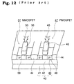
- the semiconductor integrated circuit including the four-terminal device is formed on a SOI substrate 40 in which a buried dielectric film 42 and a very thin single-crystal silicon layer 43 are formed on a supporting substrate 41, as shown in Fig. 12.
- a PMOSFET 47 mainly composed of a gate electrode 46, a gate dielectric film and source/drain regions 48
- an NMOSFET 57 mainly composed of a gate electrode 56, a gate dielectric film and source/drain regions 58.
- These FETs are isolated by a device isolation film 44.
- body contacts 45, 55 are formed near the PMOSFET 47 and the NMOSFET 57.
- the four-terminal device in a semiconductor integrated circuit having such a construction has an advantage that an electric potential of a channel portion of each transistor may be controlled by applying a voltage to the body contacts 45, 55, whereby a threshold voltage which is one of the factors determining the transistor characteristics, for example, may be dynamically changed.
- the four-terminal device having the body contacts 45, 55 has a drawback that the cell area is increased as compared with a conventional MOSFET.
- Japanese Unexamined Patent Publication No. HEI 7(1995)-74363 proposes a semiconductor device in which one well contact is formed for a plurality of MOSFETs instead of forming the well contact for each MOSFET, so as to achieve reduction of the cell area.
- a very thin silicon film having a thickness of 50 to 100 nm is used as the surface semiconductor layer, and moreover, the electric potential of the well is fixed by using the well contact, so that the leak current in the standby state is still large, leading to large electric current consumption.
- the present invention has been made in view of these circumstances and the purpose thereof is to provide a SOI semiconductor device and a method for manufacturing the same in which driving capability in an active state is improved, electric current consumption in a standby state is reduced, and also the cell area of the semiconductor device is kept to a minimum, thereby achieving further scale reduction.
- the present invention provides a SOI semiconductor device comprising: a SOI substrate in which a buried dielectric film and a surface semiconductor layer are laminated; at least one well formed in the surface semiconductor layer; and at least one transistor which is formed in the well and has a channel region and source/drain regions in the surface semiconductor layer, wherein the well is completely isolated in the surface semiconductor layer and has a well-contact for applying a bias voltage to the well, the transistor is isolated by a device isolation film formed in a surface of the surface semiconductor layer, the channel region is partially depleted, and the surface semiconductor layer under the source/drain regions is fully depleted.
- the present invention provides a method for manufacturing a SOI semiconductor device having the above-mentioned construction, wherein complete isolation of the well is achieved by forming a dielectric film that reaches the buried dielectric film in a predetermined region of the surface semiconductor layer.
- a SOI semiconductor device of the present invention is composed of a SOI substrate in which a buried dielectric film and a surface semiconductor layer are laminated; at least one well formed in the surface semiconductor layer; a well complete-isolation film that completely isolates the well (the isolation may be achieved by mesa isolation); a well contact for applying a bias voltage to the well; at least one transistor formed in the well; and a device isolation film for isolating the transistor.
- the SOI substrate may be a substrate typically formed by laminating a buried dielectric film and a surface semiconductor layer successively on a supporting substrate, so as to achieve low power consumption and high speed operation, and may be a substrate used as a bonding SOI (BESOI) or SIMOX (Separation by Implantation of Oxygen) type substrate, or the like.
- the supporting substrate may be selected from a variety of substrates such as a semiconductor substrate of silicon, germanium or the like, a compound semiconductor substrate of GaAs, InGaAs or the like, and an insulating substrate of sapphire, quartz, glass or plastics.
- the supporting substrate may include an element such as a transistor or a capacitor, or a circuit formed on the supporting substrate.
- the buried dielectric film may be, for example, an SiO 2 film or an SiN film.
- the thickness of the buried dielectric film may be suitably adjusted by considering the characteristics of the semiconductor device to be obtained, the magnitude of the applied voltage in using the obtained semiconductor device or the like.
- the thickness of the dielectric film may be, for example, about 50 to about 400 nm.
- the surface semiconductor layer is a semiconductor thin film that acts as an active layer for forming the transistor, and may be formed with a thin film made of a semiconductor such as silicon or germanium, or a compound semiconductor such as GaAs or InGaAs. Among these, a silicon thin film is preferable. It is necessary that the surface semiconductor layer has a film thickness T semi which is smaller than or equal to a sum of a depth X j of source/drain regions of a later-mentioned transistor and a width W depl of a depleted layer under the source/drain regions from a junction interface and larger than or equal to about 100 nm, i.e. about 100 nm ⁇ T semi ⁇ X j + W depl .
- the thickness of the surface semiconductor layer may be selected within the range of about 100 nm to 400 nm.
- both X j and W depl may be suitably adjusted in accordance with the characteristics of the semiconductor device to be obtained, they may be set up to about 200 nm.
- the width W depl of the depleted layer are influenced by the impurity concentration of a later-mentioned well, the magnitude of a bias voltage V W applied to the well of the obtained SOI semiconductor device, and further the dielectric constant ⁇ of the semiconductor constituting the surface semiconductor layer, the electric charge q, the magnitude of the voltage V d to be applied to the source/drain regions, a built-in voltage V bi and the like.
- the surface semiconductor layer in the SOI substrate includes at least one well.
- the well may be a p-type or n-type well.
- the concentration of the well may be suitably adjusted by considering the characteristics of the semiconductor to be obtained.
- the concentration of the well may be, for example, in the order of 10 16 to 10 18 ions/cm 3 .
- the well is completely isolated from a region of the surface semiconductor layer other than the well.
- This complete isolation of the well may be achieved by the LOCOS method in which a LOCOS oxide film is formed to extend from the surface of the surface semiconductor layer to the buried oxide film, i.e. a LOCOS film having a thickness larger than the thickness of the surface semiconductor layer.
- the complete isolation of the well may be achieved by the trench device isolation method in which a trench device isolation film is formed to extend from the surface of the surface semiconductor layer to the buried dielectric film by forming a trench in a desired region of the surface semiconductor layer and forming/burying a dielectric film in the trench, followed by an optional planarization treatment.
- the complete isolation of the well may be achieved by the mesa isolation method in which a desired region of the surface semiconductor layer is removed till the removed portion reaches the buried dielectric film.
- the LOCOS method, the trench device isolation method, and the mesa isolation method may be carried out by utilizing a known process, such as a photolithography process, an etching process, a CMP process, or the like.
- the well includes a well-contact for applying a predetermined bias voltage to the well.
- the number of well-contacts to be formed in one well may be adjusted in accordance with the size of the well, the number of transistors to be formed in the well, or the like. However, it is preferable that one well includes one well-contact in view of reduction of the area occupied by the device.
- the well-contact is typically a part of the well and may be formed by connecting an electrode to a contact region which is to become a suitable contact resistance.
- the contact region to be formed may have an impurity concentration in the order of 10 20 ions/cm 3 or more.
- the electrode may be formed of any material as long as it is an electrically conductive material that may be generally used as an electrode or a wiring layer.
- a transistor is formed at the well in the surface semiconductor layer of the SOI substrate of the present invention.
- the transistor includes a gate electrode formed via a gate oxide film and source/drain regions formed in the surface semiconductor layer on both sides of the gate electrode.
- the gate oxide film may be formed with a material and a thickness such that it generally functions as a gate electrode.
- the gate electrode may be formed to a thickness of about 150 nm to about 300 nm with a polysilicon; a silicide of a high melting point metal such as W, Ta, Ti, or Mo; a polycide made of such a silicide and polysilicon; another metal or the like.
- the gate electrode may include a sidewall spacer made of a dielectric film in view of lateral diffusion of an impurity for forming the later-mentioned source/drain regions.
- the source/drain regions may be formed to contain an impurity of a conductivity type opposite to that of the well at a concentration of about 1 ⁇ 10 20 to 1 ⁇ 10 21 ions/cm 3 .
- the source/drain regions may include a low concentration region such as an LDD structure, a region of the same degree of concentration, or a high concentration region at the end of the source/drain region on the channel side and with a depth which is a little smaller than a junction depth of the source/drain regions.
- the depth of the source/drain regions may be, for example, about 70 nm to about 200 nm, although the depth may be suitably adjusted in accordance with the characteristics of the semiconductor device to be obtained or the like.
- the transistor formed at the well is isolated from another transistor by a device isolation film.
- the device isolation film may be formed by a known device isolation method such as the LOCOS method, the trench isolation method or the like.
- the device isolation film is formed only in the surface of the well, and is not formed to extend along the entire depth of the surface semiconductor layer.
- the device isolation film is usually formed before the transistor is formed.
- the above-mentioned process of complete isolation of the well may be performed after the device isolation film is formed, or alternatively, the device isolation film may be formed in the surface of the well after the process of complete isolation of the well is performed.
- the channel region constituting the transistor is partially depleted, and the surface semiconductor layer under the source/drain regions is fully depleted.
- the partially depleted layer of the channel region means that the channel region immediately under the gate electrode is uniformly depleted between the source/drain regions, while a portion of the surface semiconductor layer under the depleted region is not depleted.
- the fully depleted layer under the source/drain region means that the portion of the surface semiconductor layer under the source/drain regions is fully or completely depleted, namely, that the portion of the surface semiconductor layer from the junction interface of the source/drain regions to the interface between the surface semiconductor layer and the buried dielectric film is fully depleted.
- the voltage applied to the well-contact is transmitted to the non-depleted region to achieve the electric potential control of the channel region. Also, since the surface semiconductor layer under the source/drain regions is fully depleted, the capacitance generated by the depleted layer extending under the source/drain regions is connected to the capacitance of the buried dielectric film in series, so that the load capacitance of the transistor may be reduced, thereby leading to low consumption of electric power and high speed operation of the device as a whole.
- the threshold voltage of the transistor can be controlled by applying a bias voltage to the well-contact and changing the bias voltage.
- a bias voltage By fixing the bias voltage to a predetermined constant voltage, it is possible to improve the driving capability of the transistor in an active state (ON-state) or to reduce the leak current or electric current consumption in a standby-state (OFF-state).
- both the effect of improvement in the driving capability and the effect of reduction in the electric current consumption may be obtained by changing the voltage between the active state and the standby state.
- the bias voltage may be selected within the range of about -2V to about 1V.
- the bias voltage may be, for example, about the power voltage in the active state, and approximately 0 V in the standby state. If the transistor is a PMOS, the bias voltage may be, for example, about -0.5 V in the active state, and about the power voltage in the standby state.
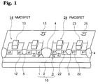
- Fig. 1 is a view showing a SOI semiconductor device of the present invention.
- the semiconductor device is formed on a SOI substrate 10 including a buried dielectric film 2 and a surface silicon layer 3 formed on a supporting substrate 1.
- the surface silicon layer 3 and the buried dielectric film 2 are formed to have a thicknesses of about 180 nm and a thickness of about 50 to about 400 nm, respectively.
- the surface silicon layer 3 includes a P-well 11 and an N-well 21 each formed to have an impurity concentration in the order of 10 16 to 10 18 ions/cm 3 .
- a well complete-isolation oxide film 4 having a thickness equal to or larger than the thickness of the surface silicon layer 3 is formed between the P-well 11 and the N-well 21 so as to completely isolate the P-well 11 and the N-well 21.
- an NMOSFET 14 is formed including source/drain regions 12 and a gate electrode 13 in an active region defined by the device isolation film 5 for isolating the MOSFETs, and further a P-well-contact 15 is formed.
- a PMOSFET 24 is formed including source/drain regions 22 and a gate electrode 23 in an active region defined by the device isolation film 5 for isolating the MOSFETs, and further an N-well-contact 25 is formed.
- the source/drain regions 12, 22 are each formed to have a junction depth of about 150 nm, whereby a depleted layer (not shown) formed under the source/drain regions 12, 22 has a width of about 30 nm.
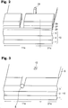
- a SOI substrate 10 is formed by forming a buried dielectric oxide film 2 of about 100 nm thickness and a surface silicon layer 3 of about 180 nm thickness on a supporting substrate 1 made of p-type silicon.
- the SOI substrate 10 is thermally oxidized at a temperature of 800°C or more to form a thermal oxide film 26 of about 7 nm thickness on the surface of the SOI substrate 10. Then, a silicon nitride film 27 of about 80 nm thickness and a photoresist 28 are deposited on the thermal oxide film 26, followed by a photolithography and etching process to pattern the photoresist 28 into a desired shape. With this photoresist 28 used as a mask, the silicon nitride film 27 is dry-etched to leave a portion of the silicon nitride film 27 at a desired location by utilizing a gas containing a mixture of CHF 3 and SF 6 .
- the photoresist 28 is removed, and thermal oxidation is performed at a temperature of 1000°C or more to form a device isolation film 5 that does not reach the depth of the surface silicon layer 3, as shown in Fig. 3. This means that the surface silicon layer 3 is not oxidized to its entire depth. Further, a well-contact 15 is formed, followed by removal of the silicon nitride film 27 by using phosphoric acid.
- the obtained SOI substrate 10 is thermally oxidized again at a temperature of 800°C or more to form a thermal oxide film 36 of 10 nm thickness on the surface of the SOI substrate 10, as shown in Fig. 4.
- a silicon nitride film 37 of about 20 nm thickness and a photoresist 38 are deposited on the thermal oxide film 36, followed by a photolithography and etching process to pattern the photoresist 38 into a desired shape.
- the silicon nitride film 37 is dry-etched to leave a portion of the silicon nitride film 37 at a desired location by utilizing a gas containing a mixture of CHF 3 and SF 6 .
- the photoresist 38 is removed, followed by thermal oxidation at a temperature of 1000°C or more to form a well complete-isolation film 4 that reaches the depth of the surface silicon layer 3, as shown in Fig. 5. This means that the surface silicon layer 3 is oxidized to its entire depth. Thereafter, the silicon nitride film 37 is removed by using phosphoric acid.
- boron ions and phosphorus ions are implanted into a P-well formation region 11a and an N-well formation region 21a, respectively, by a known method with an acceleration energy of about 60 keV and a dosage of about 7 ⁇ 10 12 cm -2 , so as to form a P-well 11 and an N-well 21 having a final impurity concentration of about 6 ⁇ 10 17 cm -3 .
- a gate dielectric film of about 10 nm thickness by thermal oxidation at around 800°C and a polysilicon film of about 200 nm thickness are formed, followed by dry etching using an HBr-based or HCl-based etching gas to form gate electrodes 13, 23 having a desired shape.
- phosphorus ions for the NMOS for example, are implanted with an acceleration energy of about 60 keV and a dosage of about 5 ⁇ 10 15 cm -2 to form source/drain regions 12, 22 having a junction depth of about 150 nm, thereby completing a SOI semiconductor device including the NMOSFET 14, the PMOSFET 24 and the like, as shown in Fig. 1.
- This process realizes a SOI semiconductor device in which the surface semiconductor layer at the channel region is partially depleted and the surface semiconductor layer at the source/drain regions is fully depleted.
- the threshold voltage of the transistor may be controlled by applying a bias voltage to the well-contact and increasing the bias voltage, namely, that the degree of freedom in the drain current may be increased by changing the bias voltage.
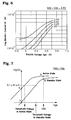
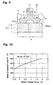
- the threshold voltage in the active state may be made smaller than the threshold voltage in the standby state by applying different bias voltages to the well between the active state and the standby state in the n-type MOS transistor of the SOI semiconductor device of the present invention, namely, by applying a high bias voltage V W (for example, 0.6 V) in the active state and applying a low voltage V W (for example, 0 V) in the standby state, as shown in Fig. 7.
- V W for example, 0.6 V
- V W for example, 0 V
- the drain current obtained by application of the same voltage as the power voltage V dd to the gate voltage V gs may be increased (point A in Fig. 7). This shows that the driving capability of the SOI semiconductor device may be improved.
- the threshold voltage in the standby state may be made larger than the threshold voltage in the active state.
- the drain current obtained by applying 0 V to the gate voltage V gs may be decreased (point X (about 100 pA/ ⁇ m) to point Y (about 0.1 pA/ ⁇ m) in Fig. 7), thereby reducing the electric current consumption in the standby state.
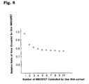
- the effect of preventing increase in the cell area was studied in the SOI semiconductor device of the present invention. Namely, in the same manner as the above Example, one or more NMOSFETs and one well-contact were formed in a P-well to measure the change in the relative ratio of the area occupied per one NMOSFET when the number of NMOSFETs per one well-contact is increased. This measurement was carried out using an NMOSFET with a gate length of 0.35 ⁇ m and a gate width of 5.0 ⁇ m. The result is shown in Fig. 8.
- the relative ratio of the area occupied by one NMOSFET was represented by a ratio relative to one body-contact, namely, (area occupied by one NMOSFET when a well-contact is used)/(area occupied by one NMOSFET when a body-contact is used), since one body-contact is always required to one NMOSFET.
- the cell area may be reduced by about 20% or more when four or more NMOSFETs, for example, are controlled by one well-contact, as compared with the case in which a semiconductor device using a body-contact is formed.
- the SOI semiconductor device of the present invention makes it possible to keep the increase in the cell area to the minimum as compared with a conventionally-used semiconductor device including a body-contact.
- the capacitance of the depleted layer 6, coupled with the capacitance of the buried dielectric film 2 can be greatly reduced by adjusting the thickness T si of the surface silicon layer 3 to be smaller than a sum of the junction depth X j of the source/drain regions 12 and the width W depl of the depleted layer 6 formed thereunder in the NMOSFET, for example, by setting the thickness T si of the surface silicon layer 3 to be about 180 nm, setting the depth X j of the source/drain regions 12 to be about 150 nm, and setting the width W depl of the depleted layer 6 to be about 30 nm. This leads to reduction in the load capacitance of the transistor and further to the achievement of high speed operation of the device as a whole.
- the SOI semiconductor device of the present invention includes a well complete-isolation film for providing complete isolation between the wells, as shown in Figs. 11(a) to 11(c). Therefore, generation of a parasitic thyristor caused by contact of the N-well and the P-well can be prevented, thereby suppressing a latch-up in the semiconductor device.
- the well complete-isolation film can also be formed by the trench isolation method instead of the above-mentioned LOCOS method.
- the surface silicon layer in the SOI substrate is thermally oxidized to form an oxide film in the surface of the surface silicon layer, and then a silicon nitride film is deposited. Subsequently, by a photolithography and etching process, an opening is formed at a region of the silicon nitride film where a well complete-isolation film is to be formed. Then, an oxide film such as TEOS is deposited in the opening. Thereafter, the surface of the oxide film is planarized by the CMP method or the like, followed by removal of the silicon nitride film with phosphoric acid to form the well complete-isolation film by trench isolation.
- the well complete-isolation film may be formed by the mesa isolation method instead of the above-mentioned LOCOS method or trench isolation method.
- a resist mask is formed which is open at a desired region in the surface silicon layer of the SOI substrate.
- the surface silicon layer at the desired region for isolation is removed by the dry-etching method using an HBr-based or HCl-based gas, so as to completely isolate the wells by mesa isolation.
- the threshold voltage of the transistor can be dynamically controlled by utilizing the well-contact. This can reduce the electric current consumption in the standby state while maintaining the high driving capability in the active state.
- the cell area can be reduced to the minimum without increase in the area occupied by the device such as in the case of a conventional four-terminal device, thereby achieving a highly efficient and highly integrated semiconductor device.
- the surface semiconductor layer has a thickness smaller than the sum of the junction depth of the source/drain regions and the width of the depleted layer formed thereunder. Therefore, the capacitance of the depleted layer is connected to the capacitance of the buried oxide film in series, whereby the load capacitance of the transistor is considerably reduced, achieving a high speed operation of the device.
Landscapes
- Thin Film Transistor (AREA)
- Element Separation (AREA)
Applications Claiming Priority (2)
| Application Number | Priority Date | Filing Date | Title |
|---|---|---|---|
| JP14148798A JP3383219B2 (ja) | 1998-05-22 | 1998-05-22 | Soi半導体装置及びその製造方法 |
| JP14148798 | 1998-05-22 |
Publications (3)
| Publication Number | Publication Date |
|---|---|
| EP0962988A2 true EP0962988A2 (de) | 1999-12-08 |
| EP0962988A3 EP0962988A3 (de) | 2000-06-14 |
| EP0962988B1 EP0962988B1 (de) | 2007-07-11 |
Family
ID=15293062
Family Applications (1)
| Application Number | Title | Priority Date | Filing Date |
|---|---|---|---|
| EP99303815A Expired - Lifetime EP0962988B1 (de) | 1998-05-22 | 1999-05-17 | SOI-Halbleiteranordnung und Verfahren zur Herstellung |
Country Status (7)
| Country | Link |
|---|---|
| US (1) | US6462379B2 (de) |
| EP (1) | EP0962988B1 (de) |
| JP (1) | JP3383219B2 (de) |
| KR (1) | KR100333168B1 (de) |
| CN (1) | CN1147003C (de) |
| DE (1) | DE69936487T2 (de) |
| TW (1) | TW432593B (de) |
Cited By (5)
| Publication number | Priority date | Publication date | Assignee | Title |
|---|---|---|---|---|
| EP1225622A3 (de) * | 2001-01-18 | 2003-11-12 | Kabushiki Kaisha Toshiba | Halbleiteranordnung und Herstellungsverfahren dafür |
| US6794717B2 (en) * | 2001-02-13 | 2004-09-21 | Renesas Technology Corp. | Semiconductor device and method of manufacturing the same |
| US6953979B1 (en) | 1998-12-24 | 2005-10-11 | Mitsubishi Denki Kabushiki Kaisha | Semiconductor device, method of manufacturing same and method of designing same |
| EP1473779A3 (de) * | 2003-04-29 | 2006-03-08 | Samsung SDI Co., Ltd. | Dünnschicht Transistor und ihn verwendende Anzeigevorrichtung |
| US8530290B2 (en) | 2007-03-09 | 2013-09-10 | Samsung Display Co., Ltd. | Thin film transistor, method of fabricating the same, and organic light emitting diode display device including the same |
Families Citing this family (17)
| Publication number | Priority date | Publication date | Assignee | Title |
|---|---|---|---|---|
| JP4540684B2 (ja) * | 1998-12-24 | 2010-09-08 | ルネサスエレクトロニクス株式会社 | 半導体装置 |
| WO2001067169A1 (en) * | 2000-03-10 | 2001-09-13 | Seiko Epson Corporation | Electrooptical device and electronic device |
| JP2001274264A (ja) | 2000-03-24 | 2001-10-05 | Mitsubishi Electric Corp | 半導体装置及びその製造方法 |
| JP2001274265A (ja) | 2000-03-28 | 2001-10-05 | Mitsubishi Electric Corp | 半導体装置 |
| JP5000055B2 (ja) * | 2001-09-19 | 2012-08-15 | ルネサスエレクトロニクス株式会社 | 半導体装置 |
| US6747318B1 (en) * | 2001-12-13 | 2004-06-08 | Lsi Logic Corporation | Buried channel devices and a process for their fabrication simultaneously with surface channel devices to produce transistors and capacitors with multiple electrical gate oxides |
| JP2003318405A (ja) * | 2002-04-25 | 2003-11-07 | Mitsubishi Electric Corp | 半導体装置およびその製造方法 |
| DE10301243B4 (de) | 2003-01-15 | 2009-04-16 | Infineon Technologies Ag | Verfahren zum Herstellen einer integrierten Schaltungsanordnung, insbesondere mit Kondensatoranordnung |
| KR100975972B1 (ko) * | 2003-07-11 | 2010-08-13 | 매그나칩 반도체 유한회사 | Cmos 트랜지스터의 구조 및 그 제조 방법 |
| SG113006A1 (en) * | 2004-01-04 | 2005-07-28 | Teradyne Inc | Silicon-on-insulator channel architecture of automatic test equipment |
| US7288802B2 (en) * | 2005-07-27 | 2007-10-30 | International Business Machines Corporation | Virtual body-contacted trigate |
| KR101198938B1 (ko) * | 2005-12-21 | 2012-11-07 | 매그나칩 반도체 유한회사 | 고전압 소자의 소자 분리 방법 |
| US7402885B2 (en) * | 2006-05-15 | 2008-07-22 | Toshiba America Electronic Components, Inc. | LOCOS on SOI and HOT semiconductor device and method for manufacturing |
| JP5328214B2 (ja) * | 2008-04-17 | 2013-10-30 | シャープ株式会社 | 半導体装置、tft基板、表示装置、携帯機器 |
| JP5269924B2 (ja) * | 2011-01-27 | 2013-08-21 | ルネサスエレクトロニクス株式会社 | 半導体装置の製造方法 |
| TWM435722U (en) | 2012-03-22 | 2012-08-11 | Excelliance Mos Corp | Power MOSFET |
| CN111240392B (zh) * | 2020-01-19 | 2021-07-27 | 中国科学院上海微系统与信息技术研究所 | 阈值电压的调节方法、装置、cmos器件、电子设备及存储介质 |
Family Cites Families (15)
| Publication number | Priority date | Publication date | Assignee | Title |
|---|---|---|---|---|
| US5463238A (en) | 1992-02-25 | 1995-10-31 | Seiko Instruments Inc. | CMOS structure with parasitic channel prevention |
| JPH05160403A (ja) * | 1992-06-01 | 1993-06-25 | Seiko Epson Corp | 薄膜トランジスタ |
| FR2694449B1 (fr) | 1992-07-09 | 1994-10-28 | France Telecom | Composant électronique multifonctions, notamment élément à résistance dynamique négative, et procédé de fabrication correspondant. |
| US5317181A (en) | 1992-09-10 | 1994-05-31 | United Technologies Corporation | Alternative body contact for fully-depleted silicon-on-insulator transistors |
| JPH06151859A (ja) | 1992-09-15 | 1994-05-31 | Canon Inc | 半導体装置 |
| JP3778581B2 (ja) * | 1993-07-05 | 2006-05-24 | 三菱電機株式会社 | 半導体装置およびその製造方法 |
| US5973363A (en) | 1993-07-12 | 1999-10-26 | Peregrine Semiconductor Corp. | CMOS circuitry with shortened P-channel length on ultrathin silicon on insulator |
| JP3247801B2 (ja) | 1993-07-27 | 2002-01-21 | 三菱電機株式会社 | Soi構造を有する半導体装置およびその製造方法 |
| JPH07302908A (ja) | 1994-05-02 | 1995-11-14 | Fujitsu Ltd | 半導体装置及びその製造方法 |
| JPH08125187A (ja) | 1994-10-24 | 1996-05-17 | Nippon Telegr & Teleph Corp <Ntt> | Soi構造mos型半導体装置およびその製造方法 |
| US5895766A (en) * | 1995-09-20 | 1999-04-20 | Micron Technology, Inc. | Method of forming a field effect transistor |
| US5770881A (en) * | 1996-09-12 | 1998-06-23 | International Business Machines Coproration | SOI FET design to reduce transient bipolar current |
| JP3447927B2 (ja) * | 1997-09-19 | 2003-09-16 | 株式会社東芝 | 半導体装置およびその製造方法 |
| US5959335A (en) * | 1998-09-23 | 1999-09-28 | International Business Machines Corporation | Device design for enhanced avalanche SOI CMOS |
| US5965917A (en) * | 1999-01-04 | 1999-10-12 | Advanced Micro Devices, Inc. | Structure and method of formation of body contacts in SOI MOSFETS to elimate floating body effects |
-
1998
- 1998-05-22 JP JP14148798A patent/JP3383219B2/ja not_active Expired - Fee Related
-
1999
- 1999-05-14 US US09/311,309 patent/US6462379B2/en not_active Expired - Fee Related
- 1999-05-17 DE DE69936487T patent/DE69936487T2/de not_active Expired - Lifetime
- 1999-05-17 EP EP99303815A patent/EP0962988B1/de not_active Expired - Lifetime
- 1999-05-17 TW TW088107990A patent/TW432593B/zh not_active IP Right Cessation
- 1999-05-20 KR KR1019990018232A patent/KR100333168B1/ko not_active Expired - Fee Related
- 1999-05-21 CN CNB991070054A patent/CN1147003C/zh not_active Expired - Fee Related
Cited By (14)
| Publication number | Priority date | Publication date | Assignee | Title |
|---|---|---|---|---|
| US7741679B2 (en) | 1998-12-24 | 2010-06-22 | Renesas Technology Corp. | Semiconductor device, method of manufacturing same and method of designing same |
| US6953979B1 (en) | 1998-12-24 | 2005-10-11 | Mitsubishi Denki Kabushiki Kaisha | Semiconductor device, method of manufacturing same and method of designing same |
| US7303950B2 (en) | 1998-12-24 | 2007-12-04 | Mitsubishi Denki Kabushiki Kaisha | Semiconductor device, method of manufacturing same and method of designing same |
| US6930361B2 (en) | 2001-01-18 | 2005-08-16 | Kabushiki Kaisha Toshiba | Semiconductor device realizing characteristics like a SOI MOSFET |
| US7400016B2 (en) | 2001-01-18 | 2008-07-15 | Kabushiki Kaisha Toshiba | Semiconductor device realizing characteristics like a SOI MOSFET |
| EP1225622A3 (de) * | 2001-01-18 | 2003-11-12 | Kabushiki Kaisha Toshiba | Halbleiteranordnung und Herstellungsverfahren dafür |
| US6794717B2 (en) * | 2001-02-13 | 2004-09-21 | Renesas Technology Corp. | Semiconductor device and method of manufacturing the same |
| US7256463B2 (en) | 2001-02-13 | 2007-08-14 | Renesas Technology Corp. | Semiconductor device having SOI structure including a load resistor of an sram memory cell |
| US8624298B2 (en) | 2003-04-29 | 2014-01-07 | Samsung Display Co., Ltd. | Display device including thin film transistor |
| US7274037B2 (en) | 2003-04-29 | 2007-09-25 | Samsung Sdi Co., Ltd. | Thin film transistor and display device using the same |
| US8013337B2 (en) | 2003-04-29 | 2011-09-06 | Samsung Mobile Display Co., Ltd. | Thin film transistor and display device using the same |
| EP1473779A3 (de) * | 2003-04-29 | 2006-03-08 | Samsung SDI Co., Ltd. | Dünnschicht Transistor und ihn verwendende Anzeigevorrichtung |
| US8652885B2 (en) | 2003-04-29 | 2014-02-18 | Samsung Display Co., Ltd. | Method of fabricating thin film transistor |
| US8530290B2 (en) | 2007-03-09 | 2013-09-10 | Samsung Display Co., Ltd. | Thin film transistor, method of fabricating the same, and organic light emitting diode display device including the same |
Also Published As
| Publication number | Publication date |
|---|---|
| TW432593B (en) | 2001-05-01 |
| KR100333168B1 (ko) | 2002-04-18 |
| JP3383219B2 (ja) | 2003-03-04 |
| EP0962988A3 (de) | 2000-06-14 |
| US20010052613A1 (en) | 2001-12-20 |
| EP0962988B1 (de) | 2007-07-11 |
| CN1236999A (zh) | 1999-12-01 |
| US6462379B2 (en) | 2002-10-08 |
| DE69936487T2 (de) | 2008-03-20 |
| DE69936487D1 (de) | 2007-08-23 |
| JPH11340465A (ja) | 1999-12-10 |
| CN1147003C (zh) | 2004-04-21 |
| KR19990088443A (ko) | 1999-12-27 |
Similar Documents
| Publication | Publication Date | Title |
|---|---|---|
| US6462379B2 (en) | SOI semiconductor device and method for manufacturing the same | |
| US6452232B1 (en) | Semiconductor device having SOI structure and manufacturing method thereof | |
| EP0749165B1 (de) | Dünnfilmtransistor über einem isolierten Halbleitersubstrat und Verfahren zur Herstellung | |
| JP3437132B2 (ja) | 半導体装置 | |
| EP0803911B1 (de) | Kanalstruktur eines Feldeffekttransistors und eines CMOS-Elements | |
| US5973364A (en) | MIS semiconductor device having body-contact region | |
| US7687365B2 (en) | CMOS structure for body ties in ultra-thin SOI (UTSOI) substrates | |
| US7259049B2 (en) | Self-aligned isolation double-gate FET | |
| JP3504212B2 (ja) | Soi構造の半導体装置 | |
| US20050282342A1 (en) | Field effect transistor and fabrication method thereof | |
| US9997607B2 (en) | Mirrored contact CMOS with self-aligned source, drain, and back-gate | |
| KR20040022387A (ko) | 동적 문턱 전압 제어를 위한 폴리실리콘 후단-게이트절연체-상-실리콘 모스펫 | |
| US6506638B1 (en) | Vertical double gate transistor structure | |
| US7105897B2 (en) | Semiconductor structure and method for integrating SOI devices and bulk devices | |
| US6166412A (en) | SOI device with double gate and method for fabricating the same | |
| EP1229576B1 (de) | Herstellungsverfahren für SOI-MOSFET | |
| JP3103159B2 (ja) | 半導体装置 | |
| US6605843B1 (en) | Fully depleted SOI device with tungsten damascene contacts and method of forming same | |
| US20020175372A1 (en) | Semiconductor device and method for manufacturing semiconductor device | |
| US7078773B2 (en) | Nitride-encapsulated FET (NNCFET) | |
| US6459106B2 (en) | Dynamic threshold voltage devices with low gate to substrate resistance | |
| JP3479066B2 (ja) | Soi構造の半導体装置及びその製造方法 | |
| JP2004146847A (ja) | 半導体装置及びその製造方法 |
Legal Events
| Date | Code | Title | Description |
|---|---|---|---|
| PUAI | Public reference made under article 153(3) epc to a published international application that has entered the european phase |
Free format text: ORIGINAL CODE: 0009012 |
|
| AK | Designated contracting states |
Kind code of ref document: A2 Designated state(s): DE FR GB IT NL |
|
| AX | Request for extension of the european patent |
Free format text: AL;LT;LV;MK;RO;SI |
|
| PUAL | Search report despatched |
Free format text: ORIGINAL CODE: 0009013 |
|
| AK | Designated contracting states |
Kind code of ref document: A3 Designated state(s): AT BE CH CY DE DK ES FI FR GB GR IE IT LI LU MC NL PT SE |
|
| AX | Request for extension of the european patent |
Free format text: AL;LT;LV;MK;RO;SI |
|
| RIC1 | Information provided on ipc code assigned before grant |
Free format text: 7H 01L 29/786 A, 7H 01L 27/12 B |
|
| 17P | Request for examination filed |
Effective date: 20000724 |
|
| AKX | Designation fees paid |
Free format text: DE FR GB IT NL |
|
| 17Q | First examination report despatched |
Effective date: 20041125 |
|
| GRAP | Despatch of communication of intention to grant a patent |
Free format text: ORIGINAL CODE: EPIDOSNIGR1 |
|
| GRAS | Grant fee paid |
Free format text: ORIGINAL CODE: EPIDOSNIGR3 |
|
| GRAA | (expected) grant |
Free format text: ORIGINAL CODE: 0009210 |
|
| AK | Designated contracting states |
Kind code of ref document: B1 Designated state(s): DE FR GB IT NL |
|
| REG | Reference to a national code |
Ref country code: GB Ref legal event code: FG4D |
|
| REF | Corresponds to: |
Ref document number: 69936487 Country of ref document: DE Date of ref document: 20070823 Kind code of ref document: P |
|
| ET | Fr: translation filed | ||
| PLBE | No opposition filed within time limit |
Free format text: ORIGINAL CODE: 0009261 |
|
| STAA | Information on the status of an ep patent application or granted ep patent |
Free format text: STATUS: NO OPPOSITION FILED WITHIN TIME LIMIT |
|
| 26N | No opposition filed |
Effective date: 20080414 |
|
| PGFP | Annual fee paid to national office [announced via postgrant information from national office to epo] |
Ref country code: GB Payment date: 20100329 Year of fee payment: 12 |
|
| PGFP | Annual fee paid to national office [announced via postgrant information from national office to epo] |
Ref country code: FR Payment date: 20100525 Year of fee payment: 12 |
|
| PGFP | Annual fee paid to national office [announced via postgrant information from national office to epo] |
Ref country code: NL Payment date: 20100518 Year of fee payment: 12 Ref country code: IT Payment date: 20100522 Year of fee payment: 12 Ref country code: DE Payment date: 20100512 Year of fee payment: 12 |
|
| REG | Reference to a national code |
Ref country code: DE Ref legal event code: R119 Ref document number: 69936487 Country of ref document: DE |
|
| REG | Reference to a national code |
Ref country code: DE Ref legal event code: R119 Ref document number: 69936487 Country of ref document: DE |
|
| REG | Reference to a national code |
Ref country code: NL Ref legal event code: V1 Effective date: 20111201 |
|
| GBPC | Gb: european patent ceased through non-payment of renewal fee |
Effective date: 20110517 |
|
| PG25 | Lapsed in a contracting state [announced via postgrant information from national office to epo] |
Ref country code: NL Free format text: LAPSE BECAUSE OF NON-PAYMENT OF DUE FEES Effective date: 20111201 |
|
| REG | Reference to a national code |
Ref country code: FR Ref legal event code: ST Effective date: 20120131 |
|
| PG25 | Lapsed in a contracting state [announced via postgrant information from national office to epo] |
Ref country code: IT Free format text: LAPSE BECAUSE OF NON-PAYMENT OF DUE FEES Effective date: 20110517 |
|
| PG25 | Lapsed in a contracting state [announced via postgrant information from national office to epo] |
Ref country code: FR Free format text: LAPSE BECAUSE OF NON-PAYMENT OF DUE FEES Effective date: 20110531 |
|
| PG25 | Lapsed in a contracting state [announced via postgrant information from national office to epo] |
Ref country code: GB Free format text: LAPSE BECAUSE OF NON-PAYMENT OF DUE FEES Effective date: 20110517 |
|
| PG25 | Lapsed in a contracting state [announced via postgrant information from national office to epo] |
Ref country code: DE Free format text: LAPSE BECAUSE OF NON-PAYMENT OF DUE FEES Effective date: 20111130 |