EP0959571A1 - Dispositif pour la réception homodyne de signaux optiques modulés par déplacement de phase - Google Patents
Dispositif pour la réception homodyne de signaux optiques modulés par déplacement de phase Download PDFInfo
- Publication number
- EP0959571A1 EP0959571A1 EP99109840A EP99109840A EP0959571A1 EP 0959571 A1 EP0959571 A1 EP 0959571A1 EP 99109840 A EP99109840 A EP 99109840A EP 99109840 A EP99109840 A EP 99109840A EP 0959571 A1 EP0959571 A1 EP 0959571A1
- Authority
- EP
- European Patent Office
- Prior art keywords
- output
- input
- feedback unit
- signal
- frequency acquisition
- Prior art date
- Legal status (The legal status is an assumption and is not a legal conclusion. Google has not performed a legal analysis and makes no representation as to the accuracy of the status listed.)
- Granted
Links
Images


Classifications
-
- H—ELECTRICITY
- H04—ELECTRIC COMMUNICATION TECHNIQUE
- H04B—TRANSMISSION
- H04B10/00—Transmission systems employing electromagnetic waves other than radio-waves, e.g. infrared, visible or ultraviolet light, or employing corpuscular radiation, e.g. quantum communication
- H04B10/60—Receivers
-
- H—ELECTRICITY
- H04—ELECTRIC COMMUNICATION TECHNIQUE
- H04B—TRANSMISSION
- H04B10/00—Transmission systems employing electromagnetic waves other than radio-waves, e.g. infrared, visible or ultraviolet light, or employing corpuscular radiation, e.g. quantum communication
- H04B10/60—Receivers
- H04B10/61—Coherent receivers
- H04B10/63—Homodyne, i.e. coherent receivers where the local oscillator is locked in frequency and phase to the carrier signal
-
- H—ELECTRICITY
- H04—ELECTRIC COMMUNICATION TECHNIQUE
- H04B—TRANSMISSION
- H04B10/00—Transmission systems employing electromagnetic waves other than radio-waves, e.g. infrared, visible or ultraviolet light, or employing corpuscular radiation, e.g. quantum communication
- H04B10/60—Receivers
- H04B10/61—Coherent receivers
- H04B10/64—Heterodyne, i.e. coherent receivers where, after the opto-electronic conversion, an electrical signal at an intermediate frequency [fIF] is obtained
-
- H—ELECTRICITY
- H04—ELECTRIC COMMUNICATION TECHNIQUE
- H04L—TRANSMISSION OF DIGITAL INFORMATION, e.g. TELEGRAPHIC COMMUNICATION
- H04L27/00—Modulated-carrier systems
- H04L27/18—Phase-modulated carrier systems, i.e. using phase-shift keying
- H04L27/22—Demodulator circuits; Receiver circuits
- H04L27/227—Demodulator circuits; Receiver circuits using coherent demodulation
- H04L27/2271—Demodulator circuits; Receiver circuits using coherent demodulation wherein the carrier recovery circuit uses only the demodulated signals
- H04L27/2272—Demodulator circuits; Receiver circuits using coherent demodulation wherein the carrier recovery circuit uses only the demodulated signals using phase locked loops
Definitions
- the invention relates to a device for the homodyne reception of optical phase-shifted signals according to the preamble of patent claim 1 .
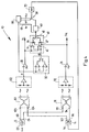
- the device 1 according to the invention according to FIG. 1 comprises a superimposition receiver, consisting of an optical coupler 11 , also called a hybrid, and an electro-optical converter 12 , also called a matching circuit, and a data decider 2 , a window comparator 3 , also a window discriminator called, and a feedback unit 4, the output of which is connected to the control input of a local oscillator laser 7 via a changeover switch 5 , which is connected downstream of a filter 6 .
- the decision maker 2 supplying the data signals Sd and the comparator 3 are connected on the input side to the output of the superimposed receiver or the E / O converter 12 .
- the unit 4 is acted upon on the one hand by the data signals Sd supplied by the decision maker 2 and on the other hand by the output signal Sb of the comparator 3 .
- the optical coupler 11 of the miniaturized heterodyne receiver has an input 111 for a received light beam of frequency fe and an input 112 for a laser beam of frequency fq supplied by laser source 7 .
- one output 113 supplies an optical sum signal and the other output 114 an optical difference signal.
- These two optical signals each act on a light-sensitive diode 121 or 122 , which they convert into corresponding electrical signals, which are added in an amplifier 123 located in the circuit 12 , the output of which supplies the analog data signal S.
- the decision maker 2 is a zero-crossing comparator which acts as a simple regenerator and outputs the digital, that is to say rectangular, data signals Sd.
- the window comparator 3 comprises two comparators 31, 32, the signal inputs of which are applied together with the output signal S of the E / O converter 12 , the output signal of the comparator 32 having the higher threshold value H and the inverted output signal of the comparator 31 having the lower one Threshold value L can be linked by an AND gate 33 .
- the feedback unit 4 comprises two AND gates 41, 42, each of which has an input connected to the output of the window comparator 3 .
- the other input of the AND gate 41 is supplied with the digital data signal Sd and the other input of the AND gate 42 with the inverted data signal Sd.
- the outputs of the AND gates 41 and 42 are each connected to an input of a differential amplifier 43 , the output of which is connected via the filter 6 and the changeover switch 5 to the control input of the local oscillator laser 7 .
- the loop filter 6 can be a low-pass filter.
- the device also includes a frequency acquisition circuit 8 inserted between the output of the E / O converter 12 and the other input of the switch 5 , which is also designed to control the switch 5 .
- the following truth table applies to the window comparator 3 according to FIG. 1 : S Sd H L Sb Sv Sw - 1 0 0 0 0 0 0 0 - 0 0 1 1 0 1 0 + 1 0 1 1 1 0 + 1 1 1 1 0 0 0 0 0 0
- S is the analog signal supplied by the E / O converter 12 , Sd the data signal obtained by the decision maker 2 , H and L the threshold value signals of the comparator 3, Sb a synchronization bit supplied by the comparator 3 and Sv and Sw the output signals of the gates 41 or 42.
- the demodulated data signal is subject to noise, phase errors and other disturbances.
- the reference axes relate to data transmission without phase errors, the points d 0 and d 1 in the real axis representing signals with a phase shift of ⁇ 90 ° for which no evaluation of the carrier phase takes place.
- the point S in the imaginary axis corresponds to a signal with a phase shift of 0 °, in which an evaluation of the carrier phase is possible.
- points d0 ', d1' and S ' are also shown, which relate to data transmission with a phase error,, the points d0' and d1 'representing signals with a phase shift of 180 °, for which none Evaluation of the carrier phase takes place.
- the point S near the point S ' corresponds to a signal with an expected phase shift of approximately 0 °, in which an evaluation of the carrier phase is possible.
- the device 9 according to the invention according to FIG. 4 comprises an in-phase heterodyne receiver, a data decider 20, a window comparator 30 and a controlled feedback unit 40, the output of which via a changeover switch 50 with an upstream filter 60 to the control input of a local oscillator -Lasers 70 is connected.
- This superimposition receiver comprises an optical coupler 101 with a downstream E / O converter 102.
- the decision maker 20 supplying the in-phase data signals Si and the window comparator 30 are connected on the input side to the output of this E / O converter 102 .
- the controlled feedback unit 40 is acted upon on the one hand by the digital data signals Si supplied by the decision maker 20 and on the other hand by the output signal of the comparator 30 .
- the device 10 according to FIG. 4 additionally has two optical beam splitters 13 and 14 , each with an input 131 for the light to be received or an input 141 for the light of the local oscillator laser 70, and a quadrature overlay receiver with a downstream data Decision maker 21 on.
- This quadrature heterodyne receiver also comprises an optical coupler 91 and an E / O converter 92, which can be constructed in the same or similar manner as elements 101 and 102 in FIG. 4 or elements 11 and 12 in FIG. 1 .
- the data decision makers 20 and 21 in FIG. 4 can also be constructed in the same way as the decision maker 2 in FIG. 1 .
- the same applies to the elements 30, 50, 60, 70 and 80 in Fig. 4 which can be connected to the elements 3, 5, 6, 7 and 8 in Fig. 1 per se the same and among themselves in the same way.
- the optical couplers 91 and 101 of these miniaturized superimposed receivers known per se each have two inputs 93 and 94 or 103 and 104 .
- the optical beam splitters 13 and 14 each have two outputs 133, 134 and 143, 144 , respectively, the outputs 133 and 143 with the inputs 103 and 104 of the coupler 101 of the in-phase channel and the outputs 134 and 144 with the inputs 93 and 94 of the coupler 91 of the quadrature channel are connected.
- the decision maker 21 is also a simple regenerator, which acts as a zero crossing comparator. It supplies digital data signals, namely the data signals Sq of the quadrature channel, which according to the invention are additionally fed to the control input of the controlled feedback unit 40 .
- the feedback unit 40 comprises two AND gates 44, 45 , each of which has an input connected in common to the output of the window comparator 30 .
- the other input of the AND gate 44 is supplied with the digital data signal Si and the other input of the AND gate 45 with the inverted data signal Si.
- the outputs of the AND gates 44 and 45 are each connected to an input of a modulo-2 adder 46 and 47 , which each have a second inverting input, which are connected to the output of the decision 21 .
- the outputs of the adders 46 and 47 are each connected to an input of a differential amplifier 48 , the output of which is connected via the filter 60 and the changeover switch 50 to the control input of the local oscillator laser 70 .
- the filter 60 is the loop filter of the OPLL and can be implemented, for example, as a low-pass filter.
- the radiation supplied by the laser source 70 is fed to the input 141 of the quadrature beam splitter 14 .
- a frequency acquisition circuit 80 inserted between the output of the E / O converter 102 and the other input of the switch 50 , which additionally controls the switch 50 .
- circuits 101, 102, 20 and 30 according to FIG. 4 work in the same way as the corresponding elements 11, 12, 2 and 3 according to FIG. 1 .
- the reference axes relate to data transmission without phase errors
- the points d0 and d1 in the real axis representing signals with a phase shift of ⁇ 90 ° for which no evaluation of the carrier phase takes place.
- the points S1 and S2 in the imaginary axis correspond to signals with a phase shift of 0 ° or 180 °, for which an evaluation of the carrier phase is possible.
- points d0 ', d1' and S1 ', S2' are also shown, which relate to data transmission with a phase error ⁇ , the points d0 'and d1' representing signals with a phase shift of ⁇ 90 ° for which there is no evaluation of the carrier phase.
- Fig. 5 In Fig. 5 below are the corresponding voltage values of the signals d0; d0 '; S2 '; S1, S2; S1 '; d1 '; d1 and in FIG. 6 below with dotted parallel lines, the lower limit voltage L ( FIG. 4 ) and the higher limit voltage H ( FIG. 4 ) of the window discriminator 30 for the in-phase channel and on the right for the quadrature channel.
- the receive voltage is positive at ⁇ > 0 and negative at ⁇ ⁇ 0.
- the corresponding voltage values of the signals S1, d1, d1, S2, d0, d1, S1, d0 are shown on the right in FIG. 6 .
- the frequency acquisition circuit 8 or 80 comprises a microprocessor 81, to which a detector 82 and a control circuit 83 are connected, and a filter bank 84.
- the microprocessor 81 is started with a start signal S0.
- the detector 82 connected to the E / O converter 12 or 102 decides whether a real signal S is present or not, and accordingly supplies a signal 1 or 0 to the microprocessor 81.
- the filter bank 84 which is connected to the via a line 49 guided output signal Sr of the feedback unit 4 or 40 is applied and a number n frequency error ranges, z. B.
- control circuit 83 which is connected via a bus 86 to the microprocessor 81 , which provides a control signal Su for the changeover switch 5 or 50 .
- the control circuit 83 in turn supplies a signal Sf which can be supplied to the local oscillator laser 7 or 70 via the changeover switch 5 or 50 .
- the frequency acquisition circuit 8 or 80 continues to function:
- the input signal S0 first starts a rough frequency search of the LO laser 7 or 70, which is then switched to control by the frequency acquisition circuit 8 or 80 via the changeover switch 5 or 50 .
- a signal S is detected in a second method step at the input of the detector 82 , that is, if the LO laser is now in the vicinity of the target frequency, the tuning speed is significantly reduced by the microprocessor 81 in order to start a fine search .
- the frequency error that is to say the signal Sr
- the signal Sr is regulated to zero.
- the signal Sr can also be routed via line 49 of the frequency acquisition circuit 8 or 80 for evaluation.
- the frequency acquisition circuit 8 or 80 switches to normal operation and from this moment the LO laser 7 or 70 is now regulated via the loop filter 6 or 60 .
- the frequency acquisition is achieved, for example, when the signal Sr no longer oscillates.
- the superimposed receivers mentioned are miniaturized components known per se (optical hybrid + balanced receiver).
- the frequency acquisition circuit 8 or 80 has the effect that the frequency fq of the unmodulated laser beam supplied by the laser source is regulated in order to achieve a match of this frequency fq with the frequency fe of the received modulated light beam.
- a phase control of the local laser source is carried out by the window discriminator circuit until the phase is locked. If the frequency synchronization fails, the changeover switch 5 or 50 is switched back to the frequency acquisition circuit 8 or 80 . When the frequency synchronization is reached, the switch switches again to the window discriminator circuit.
- the mode of operation of the device according to the invention is therefore largely independent from the applied frequency acquisition algorithm.
- the use of the window discriminator circuit or the window comparator for The determination enables the homodyne reception of optical phase-shift keyed signals the phase of the optical carrier signal and thus the phase control of the local Laser source.
- the phase control uses orthogonal carrier states that either injected, or already, as in the QPSK (Quadrature Phase Shift Keying), are available per se.
- QPSK Quadrature Phase Shift Keying
- the Threshold decision makers of the standard receiver by two or more additional ones Thresholds expanded.
- the device can also be used in the QASK (Quadrature Amplitude Shift Keying) or with the BPSK process (Binary Phase Shift Keying) with possible Synchronization signals are used.
- connection 49 between the output of the feedback unit 4 or 40 and the frequency acquisition circuit 8 or 80 can also be omitted. It is preferably used when the tuning speed is large in relation to the bandwidth of the optical control loop.
- the modulated radiation received by the inputs 111 and 131 can be circularly polarized. With the help of an upstream ⁇ / 4 plate, it can be converted to a linearly polarized wave. Additional means for regulating the polarization can be used at the output of the LO laser 7 or 70 .
- the device according to the invention is outstandingly characterized by a great long-term stability. In addition, their implementation is very inexpensive.
Applications Claiming Priority (2)
| Application Number | Priority Date | Filing Date | Title |
|---|---|---|---|
| CH213098 | 1998-10-22 | ||
| CH213098 | 1998-10-22 |
Publications (2)
| Publication Number | Publication Date |
|---|---|
| EP0959571A1 true EP0959571A1 (fr) | 1999-11-24 |
| EP0959571B1 EP0959571B1 (fr) | 2001-08-29 |
Family
ID=4226587
Family Applications (1)
| Application Number | Title | Priority Date | Filing Date |
|---|---|---|---|
| EP99109840A Expired - Lifetime EP0959571B1 (fr) | 1998-10-22 | 1999-05-19 | Dispositif pour la réception homodyne de signaux optiques modulés par déplacement de phase |
Country Status (5)
| Country | Link |
|---|---|
| US (1) | US6704375B1 (fr) |
| EP (1) | EP0959571B1 (fr) |
| JP (1) | JP2000134159A (fr) |
| CA (1) | CA2276919A1 (fr) |
| DE (1) | DE59900216D1 (fr) |
Families Citing this family (9)
| Publication number | Priority date | Publication date | Assignee | Title |
|---|---|---|---|---|
| US6819879B1 (en) * | 1999-12-29 | 2004-11-16 | Nortel Networks Limited | Method and apparatus for encoding optical power and non-payload data in an optical signal |
| US7599627B2 (en) | 2001-05-31 | 2009-10-06 | Teradvance Communications, Llc | Method and system for a polarization mode dispersion tolerant optical homodyne detection system with optimized transmission modulation |
| US20040208646A1 (en) * | 2002-01-18 | 2004-10-21 | Seemant Choudhary | System and method for multi-level phase modulated communication |
| CN101442364B (zh) * | 2007-11-19 | 2011-10-19 | 富士通株式会社 | 光相干接收机、光相干接收机用频差估计装置及方法 |
| US8401399B2 (en) | 2009-05-28 | 2013-03-19 | Freedom Photonics, Llc. | Chip-based advanced modulation format transmitter |
| US9344196B1 (en) | 2009-05-28 | 2016-05-17 | Freedom Photonics, Llc. | Integrated interferometric optical transmitter |
| US8526823B2 (en) | 2010-09-28 | 2013-09-03 | Acacia Communications, Inc. | Reconfigurable DSP performance in optical transceivers |
| US10320152B2 (en) | 2017-03-28 | 2019-06-11 | Freedom Photonics Llc | Tunable laser |
| US11923908B2 (en) * | 2021-03-19 | 2024-03-05 | The Trustees Of The University Of Pennsylvania | Integrated coherent receiver with off PLL bandwidth demodulation |
Citations (5)
| Publication number | Priority date | Publication date | Assignee | Title |
|---|---|---|---|---|
| US4037171A (en) * | 1976-02-17 | 1977-07-19 | Bell Telephone Laboratories, Incorporated | High speed tone decoder utilizing a phase-locked loop |
| US4423390A (en) * | 1981-01-09 | 1983-12-27 | Harris Corporation | Side lock avoidance network for PSK demodulator |
| US5007106A (en) * | 1989-11-08 | 1991-04-09 | At&T Bell Laboratories | Optical Homodyne Receiver |
| DE4110138C1 (en) * | 1991-03-27 | 1992-03-05 | Deutsche Forschungsanstalt Fuer Luft- Und Raumfahrt Ev, 5300 Bonn, De | Carrier recovery for optical PSK homodyne receiver - by rotating local oscillator phase 90 deg. for one synchronisation bit period to produce phase error signal |
| EP0535494A2 (fr) * | 1991-10-01 | 1993-04-07 | Siemens Aktiengesellschaft | Récepteur homodyne optique pour signaux PSK |
Family Cites Families (14)
| Publication number | Priority date | Publication date | Assignee | Title |
|---|---|---|---|---|
| JPH0239131A (ja) * | 1988-07-29 | 1990-02-08 | Hitachi Ltd | 周波数間隔安定化方法、光ヘテロダイン又は光ホモダイン通信方法 |
| JP3001943B2 (ja) * | 1990-08-30 | 2000-01-24 | 株式会社東芝 | 偏波スイッチング光源、光受信装置及びコヒーレント光伝送システム |
| JPH04144320A (ja) * | 1990-10-05 | 1992-05-18 | Hitachi Ltd | ホモダイン光受信装置 |
| JP2798526B2 (ja) * | 1991-06-20 | 1998-09-17 | 富士通株式会社 | 周波数弁別器 |
| DE69200654T2 (de) * | 1991-08-30 | 1995-05-24 | Philips Nv | Abstimmbarer Laseroszillator. |
| GB2260046B (en) * | 1991-09-26 | 1995-02-15 | Northern Telecom Ltd | Optical communications systems |
| GB2264834A (en) * | 1992-02-25 | 1993-09-08 | Northern Telecom Ltd | Optical transmission system |
| JPH077390A (ja) * | 1993-06-18 | 1995-01-10 | Uniden Corp | 高速走査無線受信機およびサーチ/スキャン誤停止防止方法 |
| DE4331882A1 (de) * | 1993-09-20 | 1995-03-23 | Siemens Ag | Verfahren zum Betrieb optischer Überlagerungsempfänger mit einer einen Fangbereich aufweisenden Regeleinrichtung zum Regeln einer Zwischenfrequenz des Empfängers auf einen Sollwert und Empfänger zur Durchführung eines solchen Verfahrens |
| JP3231545B2 (ja) * | 1994-06-28 | 2001-11-26 | 富士通株式会社 | 光周波数安定化装置 |
| JP3866283B2 (ja) * | 1994-09-14 | 2007-01-10 | コーニンクレッカ フィリップス エレクトロニクス エヌ ヴィ | 無線伝送システム及びこのシステムに用いる無線装置 |
| US5657307A (en) * | 1995-03-10 | 1997-08-12 | Sharp Kabushiki Kaisha | Optical data reading apparatus and method |
| DE19514386A1 (de) * | 1995-04-19 | 1996-10-24 | Hertz Inst Heinrich | Optischer Frequenzgenerator |
| US5687261A (en) * | 1996-01-24 | 1997-11-11 | California Institute Of Technology | Fiber-optic delay-line stabilization of heterodyne optical signal generator and method using same |
-
1999
- 1999-05-19 DE DE59900216T patent/DE59900216D1/de not_active Expired - Lifetime
- 1999-05-19 EP EP99109840A patent/EP0959571B1/fr not_active Expired - Lifetime
- 1999-07-06 CA CA002276919A patent/CA2276919A1/fr not_active Abandoned
- 1999-07-14 JP JP11200296A patent/JP2000134159A/ja active Pending
- 1999-07-28 US US09/363,301 patent/US6704375B1/en not_active Expired - Fee Related
Patent Citations (5)
| Publication number | Priority date | Publication date | Assignee | Title |
|---|---|---|---|---|
| US4037171A (en) * | 1976-02-17 | 1977-07-19 | Bell Telephone Laboratories, Incorporated | High speed tone decoder utilizing a phase-locked loop |
| US4423390A (en) * | 1981-01-09 | 1983-12-27 | Harris Corporation | Side lock avoidance network for PSK demodulator |
| US5007106A (en) * | 1989-11-08 | 1991-04-09 | At&T Bell Laboratories | Optical Homodyne Receiver |
| DE4110138C1 (en) * | 1991-03-27 | 1992-03-05 | Deutsche Forschungsanstalt Fuer Luft- Und Raumfahrt Ev, 5300 Bonn, De | Carrier recovery for optical PSK homodyne receiver - by rotating local oscillator phase 90 deg. for one synchronisation bit period to produce phase error signal |
| EP0535494A2 (fr) * | 1991-10-01 | 1993-04-07 | Siemens Aktiengesellschaft | Récepteur homodyne optique pour signaux PSK |
Non-Patent Citations (1)
| Title |
|---|
| BARRY J R ET AL: "CARRIER SYNCHRONIZATION FOR HOMODYNE AND HETERODYNE DETECTION OF OPTICAL QUADRIPHASE-SHIFT KEYING", JOURNAL OF LIGHTWAVE TECHNOLOGY, vol. 10, no. 12, 1 December 1992 (1992-12-01), pages 1939 - 1951, XP000367897 * |
Also Published As
| Publication number | Publication date |
|---|---|
| US6704375B1 (en) | 2004-03-09 |
| EP0959571B1 (fr) | 2001-08-29 |
| JP2000134159A (ja) | 2000-05-12 |
| DE59900216D1 (de) | 2001-10-04 |
| CA2276919A1 (fr) | 2000-04-22 |
Similar Documents
| Publication | Publication Date | Title |
|---|---|---|
| DE3111729C2 (fr) | ||
| DE602005006231T2 (de) | Verfahren und Vorrichtung zur kohärenten Demodulation von BPSK (binäre Phasensprungmodulation)-Signalen | |
| DE2918857C2 (fr) | ||
| DE2646255A1 (de) | Digitales detektorsystem fuer differentielle phasenshift-umtastsignale | |
| DE3243464A1 (de) | Verfahren zur kohaerenten erfassung und demodulation einer sich in irgendeinem polarisationszustand befindenden, phasenmodulierten traegerwelle und vorrichtung zur durchfuehrung des verfahrens | |
| DE2359465A1 (de) | Diversity-empfangsanlage | |
| DE2749434A1 (de) | Nullsteuereinrichtung fuer einen mehrfach-antennenbereich | |
| DE4216027A1 (de) | Demodulierschaltkreis | |
| EP0959571B1 (fr) | Dispositif pour la réception homodyne de signaux optiques modulés par déplacement de phase | |
| DE2656924C3 (de) | Phasendiskriminator in einem Empfänger eines Datenübertragungssystems | |
| DE3739484C2 (fr) | ||
| DE3902826C2 (fr) | ||
| DE4191618B4 (de) | Programmierbarer digitaler Frequenz-Phasen-Diskriminator | |
| DE69829757T2 (de) | Drei-Tor-Schaltung Empfänger | |
| DE2913172B2 (de) | Empfänger für hochfrequente elektromagneitsche Schwingungen mit einer Frequenznachregelung | |
| DE2654276B2 (de) | Phasensynchronisierende Schaltungsanordnung | |
| DE2746979C2 (de) | Anordnung zur Synchrondemodulation eines zweiseitenbandamplitudenmodulierten Signals mit oder ohne Trägerfrequenzkomponente | |
| CH676405A5 (fr) | ||
| DE69927957T2 (de) | Demodulator mit Rotationsmitteln für Frequenzverschiebungskorrektur | |
| DE3216088A1 (de) | Vorrichtung zur erkennung von signalen, die wenigstens ein erstes und ein zweites auf einer traegerwelle aufmoduliertes signal umfassen | |
| DE69835101T2 (de) | Digitaler Demodulator | |
| DE3131185C2 (de) | Empfänger für pseudozufällig phasenmodulierte Signale | |
| EP0401558A2 (fr) | Méthode pour réaliser un récepteur optique hétérodyne insensible à la phase et/ou à la polarisation pour un signal d'émission modulé en DPSK ou ASK | |
| DE4103687C2 (de) | Phasenregelschleife zur Demodulation | |
| EP0319788B1 (fr) | Récepteur optique hétérodyne pour signaux numériques |
Legal Events
| Date | Code | Title | Description |
|---|---|---|---|
| PUAI | Public reference made under article 153(3) epc to a published international application that has entered the european phase |
Free format text: ORIGINAL CODE: 0009012 |
|
| AK | Designated contracting states |
Kind code of ref document: A1 Designated state(s): BE CH DE FR GB IT LI SE |
|
| AX | Request for extension of the european patent |
Free format text: AL;LT;LV;MK;RO;SI |
|
| 17P | Request for examination filed |
Effective date: 19991013 |
|
| 17Q | First examination report despatched |
Effective date: 20000117 |
|
| RAP1 | Party data changed (applicant data changed or rights of an application transferred) |
Owner name: CONTRAVES SPACE AG |
|
| AKX | Designation fees paid |
Free format text: BE CH DE FR GB IT LI SE |
|
| GRAG | Despatch of communication of intention to grant |
Free format text: ORIGINAL CODE: EPIDOS AGRA |
|
| GRAG | Despatch of communication of intention to grant |
Free format text: ORIGINAL CODE: EPIDOS AGRA |
|
| GRAH | Despatch of communication of intention to grant a patent |
Free format text: ORIGINAL CODE: EPIDOS IGRA |
|
| GRAH | Despatch of communication of intention to grant a patent |
Free format text: ORIGINAL CODE: EPIDOS IGRA |
|
| GRAA | (expected) grant |
Free format text: ORIGINAL CODE: 0009210 |
|
| AK | Designated contracting states |
Kind code of ref document: B1 Designated state(s): BE CH DE FR GB IT LI SE |
|
| REG | Reference to a national code |
Ref country code: CH Ref legal event code: EP |
|
| REF | Corresponds to: |
Ref document number: 59900216 Country of ref document: DE Date of ref document: 20011004 |
|
| REG | Reference to a national code |
Ref country code: CH Ref legal event code: NV Representative=s name: OK PAT AG PATENTE MARKEN LIZENZEN |
|
| GBT | Gb: translation of ep patent filed (gb section 77(6)(a)/1977) |
Effective date: 20011117 |
|
| ET | Fr: translation filed | ||
| REG | Reference to a national code |
Ref country code: GB Ref legal event code: IF02 |
|
| PG25 | Lapsed in a contracting state [announced via postgrant information from national office to epo] |
Ref country code: SE Free format text: LAPSE BECAUSE OF NON-PAYMENT OF DUE FEES Effective date: 20020520 |
|
| PGFP | Annual fee paid to national office [announced via postgrant information from national office to epo] |
Ref country code: BE Payment date: 20020527 Year of fee payment: 4 |
|
| PLBE | No opposition filed within time limit |
Free format text: ORIGINAL CODE: 0009261 |
|
| STAA | Information on the status of an ep patent application or granted ep patent |
Free format text: STATUS: NO OPPOSITION FILED WITHIN TIME LIMIT |
|
| 26N | No opposition filed | ||
| EUG | Se: european patent has lapsed | ||
| PG25 | Lapsed in a contracting state [announced via postgrant information from national office to epo] |
Ref country code: GB Free format text: LAPSE BECAUSE OF NON-PAYMENT OF DUE FEES Effective date: 20030519 |
|
| PG25 | Lapsed in a contracting state [announced via postgrant information from national office to epo] |
Ref country code: BE Free format text: LAPSE BECAUSE OF NON-PAYMENT OF DUE FEES Effective date: 20030531 |
|
| BERE | Be: lapsed |
Owner name: *CONTRAVES SPACE A.G. Effective date: 20030531 |
|
| GBPC | Gb: european patent ceased through non-payment of renewal fee |
Effective date: 20030519 |
|
| PG25 | Lapsed in a contracting state [announced via postgrant information from national office to epo] |
Ref country code: IT Free format text: LAPSE BECAUSE OF NON-PAYMENT OF DUE FEES Effective date: 20050519 |
|
| REG | Reference to a national code |
Ref country code: CH Ref legal event code: PFA Owner name: OERLIKON SPACE AG Free format text: CONTRAVES SPACE AG#SCHAFFHAUSERSTRASSE 580#8052 ZUERICH (CH) -TRANSFER TO- OERLIKON SPACE AG#SCHAFFHAUSERSTRASSE 580#8052 ZUERICH (CH) |
|
| REG | Reference to a national code |
Ref country code: FR Ref legal event code: CD |
|
| REG | Reference to a national code |
Ref country code: FR Ref legal event code: PLFP Year of fee payment: 18 |
|
| REG | Reference to a national code |
Ref country code: DE Ref legal event code: R082 Ref document number: 59900216 Country of ref document: DE Representative=s name: RACH, WERNER, DIPL.-CHEM. DR.RER.NAT., DE Ref country code: DE Ref legal event code: R081 Ref document number: 59900216 Country of ref document: DE Owner name: THALES ALENIA SPACE SCHWEIZ AG, CH Free format text: FORMER OWNER: OERLIKON SPACE AG, ZUERICH, CH Ref country code: DE Ref legal event code: R081 Ref document number: 59900216 Country of ref document: DE Owner name: OEI OPTO AG, CH Free format text: FORMER OWNER: OERLIKON SPACE AG, ZUERICH, CH |
|
| REG | Reference to a national code |
Ref country code: CH Ref legal event code: PUE Owner name: OEI OPTO AG, CH Free format text: FORMER OWNER: OERLIKON SPACE AG, CH |
|
| REG | Reference to a national code |
Ref country code: CH Ref legal event code: NV Representative=s name: TROESCH SCHEIDEGGER WERNER AG, CH |
|
| REG | Reference to a national code |
Ref country code: FR Ref legal event code: TP Owner name: RUAG SCHWEIZ AG, CH Effective date: 20170213 |
|
| REG | Reference to a national code |
Ref country code: FR Ref legal event code: PLFP Year of fee payment: 19 |
|
| PGFP | Annual fee paid to national office [announced via postgrant information from national office to epo] |
Ref country code: CH Payment date: 20170505 Year of fee payment: 19 Ref country code: DE Payment date: 20170516 Year of fee payment: 19 Ref country code: FR Payment date: 20170413 Year of fee payment: 19 |
|
| REG | Reference to a national code |
Ref country code: CH Ref legal event code: NV Representative=s name: ISLER AND PEDRAZZINI AG, CH |
|
| REG | Reference to a national code |
Ref country code: CH Ref legal event code: PFA Owner name: THALES ALENIA SPACE SCHWEIZ AG, CH Free format text: FORMER OWNER: OEI OPTO AG, CH |
|
| REG | Reference to a national code |
Ref country code: DE Ref legal event code: R082 Ref document number: 59900216 Country of ref document: DE Representative=s name: RACH, WERNER, DIPL.-CHEM. DR.RER.NAT., DE Ref country code: DE Ref legal event code: R081 Ref document number: 59900216 Country of ref document: DE Owner name: THALES ALENIA SPACE SCHWEIZ AG, CH Free format text: FORMER OWNER: OEI OPTO AG, ZUERICH, CH |
|
| REG | Reference to a national code |
Ref country code: DE Ref legal event code: R119 Ref document number: 59900216 Country of ref document: DE |
|
| REG | Reference to a national code |
Ref country code: CH Ref legal event code: PL |
|
| PG25 | Lapsed in a contracting state [announced via postgrant information from national office to epo] |
Ref country code: CH Free format text: LAPSE BECAUSE OF NON-PAYMENT OF DUE FEES Effective date: 20180531 Ref country code: LI Free format text: LAPSE BECAUSE OF NON-PAYMENT OF DUE FEES Effective date: 20180531 |
|
| PG25 | Lapsed in a contracting state [announced via postgrant information from national office to epo] |
Ref country code: FR Free format text: LAPSE BECAUSE OF NON-PAYMENT OF DUE FEES Effective date: 20180531 Ref country code: DE Free format text: LAPSE BECAUSE OF NON-PAYMENT OF DUE FEES Effective date: 20181201 |