EP0938656B1 - Messvorrichtung mit einem planaren optischen wellenleiter - Google Patents
Messvorrichtung mit einem planaren optischen wellenleiter Download PDFInfo
- Publication number
- EP0938656B1 EP0938656B1 EP97954883A EP97954883A EP0938656B1 EP 0938656 B1 EP0938656 B1 EP 0938656B1 EP 97954883 A EP97954883 A EP 97954883A EP 97954883 A EP97954883 A EP 97954883A EP 0938656 B1 EP0938656 B1 EP 0938656B1
- Authority
- EP
- European Patent Office
- Prior art keywords
- radiation
- waveguide
- layer
- coupling
- excitation radiation
- Prior art date
- Legal status (The legal status is an assumption and is not a legal conclusion. Google has not performed a legal analysis and makes no representation as to the accuracy of the status listed.)
- Expired - Lifetime
Links
- 230000003287 optical effect Effects 0.000 title claims abstract description 14
- 238000005259 measurement Methods 0.000 title description 14
- 230000005855 radiation Effects 0.000 claims abstract description 117
- 230000005284 excitation Effects 0.000 claims abstract description 68
- 230000008878 coupling Effects 0.000 claims abstract description 54
- 238000010168 coupling process Methods 0.000 claims abstract description 54
- 238000005859 coupling reaction Methods 0.000 claims abstract description 54
- 239000000463 material Substances 0.000 claims abstract description 35
- 238000004458 analytical method Methods 0.000 claims abstract description 16
- 238000007789 sealing Methods 0.000 claims abstract description 8
- 239000012491 analyte Substances 0.000 claims description 23
- 238000004020 luminiscence type Methods 0.000 claims description 17
- 238000000034 method Methods 0.000 claims description 14
- 230000003595 spectral effect Effects 0.000 claims description 9
- -1 polysiloxane Polymers 0.000 claims description 6
- 229920001296 polysiloxane Polymers 0.000 claims description 2
- 230000035515 penetration Effects 0.000 abstract description 11
- 239000010410 layer Substances 0.000 description 56
- 239000000523 sample Substances 0.000 description 45
- 239000007788 liquid Substances 0.000 description 23
- 238000013016 damping Methods 0.000 description 18
- 230000004048 modification Effects 0.000 description 9
- 238000012986 modification Methods 0.000 description 9
- 238000004519 manufacturing process Methods 0.000 description 8
- 239000000853 adhesive Substances 0.000 description 5
- 239000000758 substrate Substances 0.000 description 5
- 230000001419 dependent effect Effects 0.000 description 4
- 238000001514 detection method Methods 0.000 description 4
- 239000000975 dye Substances 0.000 description 4
- 229920001971 elastomer Polymers 0.000 description 4
- 239000000806 elastomer Substances 0.000 description 4
- 239000000243 solution Substances 0.000 description 4
- 238000011161 development Methods 0.000 description 3
- 230000018109 developmental process Effects 0.000 description 3
- 235000013870 dimethyl polysiloxane Nutrition 0.000 description 3
- 239000011521 glass Substances 0.000 description 3
- 238000000465 moulding Methods 0.000 description 3
- 229920000435 poly(dimethylsiloxane) Polymers 0.000 description 3
- 238000001179 sorption measurement Methods 0.000 description 3
- 239000000126 substance Substances 0.000 description 3
- 230000002745 absorbent Effects 0.000 description 2
- 239000002250 absorbent Substances 0.000 description 2
- 238000010521 absorption reaction Methods 0.000 description 2
- 239000002318 adhesion promoter Substances 0.000 description 2
- 230000001070 adhesive effect Effects 0.000 description 2
- 230000008901 benefit Effects 0.000 description 2
- 230000027455 binding Effects 0.000 description 2
- 230000006735 deficit Effects 0.000 description 2
- 239000004205 dimethyl polysiloxane Substances 0.000 description 2
- 230000005670 electromagnetic radiation Effects 0.000 description 2
- 230000003993 interaction Effects 0.000 description 2
- 238000005304 joining Methods 0.000 description 2
- 239000003550 marker Substances 0.000 description 2
- 229920000515 polycarbonate Polymers 0.000 description 2
- 239000004417 polycarbonate Substances 0.000 description 2
- 239000002861 polymer material Substances 0.000 description 2
- 238000003825 pressing Methods 0.000 description 2
- 230000035945 sensitivity Effects 0.000 description 2
- 238000007493 shaping process Methods 0.000 description 2
- 230000001629 suppression Effects 0.000 description 2
- 230000003746 surface roughness Effects 0.000 description 2
- 230000007704 transition Effects 0.000 description 2
- 229910010413 TiO 2 Inorganic materials 0.000 description 1
- 229920004482 WACKER® Polymers 0.000 description 1
- 239000011358 absorbing material Substances 0.000 description 1
- 230000006978 adaptation Effects 0.000 description 1
- 239000012790 adhesive layer Substances 0.000 description 1
- 239000000538 analytical sample Substances 0.000 description 1
- 238000000149 argon plasma sintering Methods 0.000 description 1
- 230000004888 barrier function Effects 0.000 description 1
- 230000002146 bilateral effect Effects 0.000 description 1
- 238000012742 biochemical analysis Methods 0.000 description 1
- 239000006229 carbon black Substances 0.000 description 1
- 238000005266 casting Methods 0.000 description 1
- 230000008859 change Effects 0.000 description 1
- 238000006243 chemical reaction Methods 0.000 description 1
- 239000011248 coating agent Substances 0.000 description 1
- 238000000576 coating method Methods 0.000 description 1
- 238000013461 design Methods 0.000 description 1
- 238000009826 distribution Methods 0.000 description 1
- 230000000694 effects Effects 0.000 description 1
- 238000005516 engineering process Methods 0.000 description 1
- 229920005570 flexible polymer Polymers 0.000 description 1
- 238000002795 fluorescence method Methods 0.000 description 1
- 238000000227 grinding Methods 0.000 description 1
- 238000007654 immersion Methods 0.000 description 1
- 238000010348 incorporation Methods 0.000 description 1
- 239000007924 injection Substances 0.000 description 1
- 238000002347 injection Methods 0.000 description 1
- 229910010272 inorganic material Inorganic materials 0.000 description 1
- 239000011147 inorganic material Substances 0.000 description 1
- 238000010849 ion bombardment Methods 0.000 description 1
- 150000002500 ions Chemical class 0.000 description 1
- 230000001788 irregular Effects 0.000 description 1
- 230000031700 light absorption Effects 0.000 description 1
- 238000000691 measurement method Methods 0.000 description 1
- 229910052751 metal Inorganic materials 0.000 description 1
- 239000002184 metal Substances 0.000 description 1
- 229910044991 metal oxide Inorganic materials 0.000 description 1
- 150000004706 metal oxides Chemical class 0.000 description 1
- 150000002739 metals Chemical class 0.000 description 1
- 238000003801 milling Methods 0.000 description 1
- 239000000203 mixture Substances 0.000 description 1
- 230000007935 neutral effect Effects 0.000 description 1
- 229920000620 organic polymer Polymers 0.000 description 1
- 239000000049 pigment Substances 0.000 description 1
- 229920000058 polyacrylate Polymers 0.000 description 1
- 229920000728 polyester Polymers 0.000 description 1
- 229920000193 polymethacrylate Polymers 0.000 description 1
- 238000002360 preparation method Methods 0.000 description 1
- 230000008569 process Effects 0.000 description 1
- 238000004080 punching Methods 0.000 description 1
- 239000010453 quartz Substances 0.000 description 1
- 229920005989 resin Polymers 0.000 description 1
- 239000011347 resin Substances 0.000 description 1
- 230000009834 selective interaction Effects 0.000 description 1
- 239000011265 semifinished product Substances 0.000 description 1
- 238000000926 separation method Methods 0.000 description 1
- VYPSYNLAJGMNEJ-UHFFFAOYSA-N silicon dioxide Inorganic materials O=[Si]=O VYPSYNLAJGMNEJ-UHFFFAOYSA-N 0.000 description 1
- 229920002379 silicone rubber Polymers 0.000 description 1
- 239000004945 silicone rubber Substances 0.000 description 1
- 239000002356 single layer Substances 0.000 description 1
- 230000009870 specific binding Effects 0.000 description 1
- 238000011895 specific detection Methods 0.000 description 1
- 238000003860 storage Methods 0.000 description 1
- 239000002344 surface layer Substances 0.000 description 1
- 238000012549 training Methods 0.000 description 1
- 238000007740 vapor deposition Methods 0.000 description 1
Images


Classifications
-
- G—PHYSICS
- G01—MEASURING; TESTING
- G01N—INVESTIGATING OR ANALYSING MATERIALS BY DETERMINING THEIR CHEMICAL OR PHYSICAL PROPERTIES
- G01N21/00—Investigating or analysing materials by the use of optical means, i.e. using sub-millimetre waves, infrared, visible or ultraviolet light
- G01N21/62—Systems in which the material investigated is excited whereby it emits light or causes a change in wavelength of the incident light
- G01N21/63—Systems in which the material investigated is excited whereby it emits light or causes a change in wavelength of the incident light optically excited
- G01N21/64—Fluorescence; Phosphorescence
- G01N21/645—Specially adapted constructive features of fluorimeters
- G01N21/648—Specially adapted constructive features of fluorimeters using evanescent coupling or surface plasmon coupling for the excitation of fluorescence
-
- G—PHYSICS
- G01—MEASURING; TESTING
- G01N—INVESTIGATING OR ANALYSING MATERIALS BY DETERMINING THEIR CHEMICAL OR PHYSICAL PROPERTIES
- G01N21/00—Investigating or analysing materials by the use of optical means, i.e. using sub-millimetre waves, infrared, visible or ultraviolet light
- G01N21/01—Arrangements or apparatus for facilitating the optical investigation
- G01N21/03—Cuvette constructions
- G01N21/05—Flow-through cuvettes
-
- G—PHYSICS
- G01—MEASURING; TESTING
- G01N—INVESTIGATING OR ANALYSING MATERIALS BY DETERMINING THEIR CHEMICAL OR PHYSICAL PROPERTIES
- G01N21/00—Investigating or analysing materials by the use of optical means, i.e. using sub-millimetre waves, infrared, visible or ultraviolet light
- G01N21/75—Systems in which material is subjected to a chemical reaction, the progress or the result of the reaction being investigated
- G01N21/77—Systems in which material is subjected to a chemical reaction, the progress or the result of the reaction being investigated by observing the effect on a chemical indicator
- G01N21/7703—Systems in which material is subjected to a chemical reaction, the progress or the result of the reaction being investigated by observing the effect on a chemical indicator using reagent-clad optical fibres or optical waveguides
-
- G—PHYSICS
- G01—MEASURING; TESTING
- G01N—INVESTIGATING OR ANALYSING MATERIALS BY DETERMINING THEIR CHEMICAL OR PHYSICAL PROPERTIES
- G01N21/00—Investigating or analysing materials by the use of optical means, i.e. using sub-millimetre waves, infrared, visible or ultraviolet light
- G01N21/01—Arrangements or apparatus for facilitating the optical investigation
- G01N21/03—Cuvette constructions
- G01N2021/0346—Capillary cells; Microcells
Definitions
- the invention relates to a device consisting of an optical waveguide, the at least via a diffractive element for coupling excitation radiation into the waveguiding layer has, and on the waveguiding layer, a second tightly closing layer of a material located at least on the support surface in the range of the guided excitation radiation at least in the penetration depth of the evanescent field for both the excitation radiation and the evanescent excited radiation is transparent, and that at least in a part of the guided Excitation radiation has a recess for an analysis sample whose depth at least corresponds to the penetration depth of the evanescent field, and where the diffractive Element in the coupling region of the excitation radiation from the material of the second layer completely covered.
- the invention further relates to a method for the detection of evanescent to luminesce excitable molecules in an analyte sample using the Contraption.
- planar waveguides have been used in the field of biochemical analysis in particular for the generation and detection of evanescently excited radiation has been developed.
- a luminescence for example fluorescence
- the isotropic escaping into the room evanescent Excited radiation is generated by means of suitable measuring devices such as photodiodes, photomultipliers or CCD cameras.
- suitable measuring devices such as photodiodes, photomultipliers or CCD cameras.
- This method is for example in WO 95/33197 disclosed.
- affinity sensing for the specific detection of an analyte in a sample, which may consist of a complex mixture of substances, and for the binding of the analyte molecules at the surface of the waveguide, in the area of the penetration depth of the evanescent field, biochemical recognition elements either directly or via a primer layer immobilized on the waveguide surface.
- the sample is dissolved in solution, either in stop and flow or in flow, with those immobilized on the waveguide surface Detection elements brought into contact.
- a separation of the coupling element from the contact area with the sample by means of materials which have no special requirements in terms of transparency and refractive index can be a significant impairment of the light pipe, possibly even too their complete suppression, in the relevant contact area with the sample for the measurement to lead. This problem is described in more detail in Wo 97/01087.
- a countercurrent cell is described in WO 97/01087, in which by means of a guided in countercurrent to the analyte sample transparent and not specifically with the recognition elements acting reference liquid in Range of coupling elements optical waveguide achieved a sample-free barrier volume, in order to ensure constant conditions in the coupling-in region of the excitation radiation.
- This specifically for the measurement evanescently excited radiation improved embodiment it is technically relatively expensive, especially for stop / flow applications hardly usable and therefore in the sense of easy handling for a routine Use in, for example, diagnostic devices little suitable.
- a first object of the invention is a device composed of (a) a planar optical waveguide consisting of a transparent support (40) and a waveguiding layer (41), wherein the waveguide at least via a diffractive element (42) for coupling excitation radiation into the waveguiding layer and for generating an evanescent field, characterized in that (b) on the waveguiding Layer a tightly closing layer (43) rests from a material, the at least at the support surface at least 0.5 microns for both excitation radiation as Also for evanescently excited radiation is transparent, and that in at least a portion the guided excitation radiation either at least one upwardly open recess (45), or at least one connected via an inflow channel (2) and outflow channel (3), has an upwardly closed recess (6) for receiving an analytical sample, the depth of which is at least 0.5 ⁇ m, and wherein the diffractive element (42) of the tightly closing layer (43) is completely covered.
- Optical waveguide with one or two diffractive elements for coupling the excitation radiation and decoupling of the luminescence radiation and their dimensioning for Determinations of analyte molecules by the fluorescence method are known and the Example in WO 95/33197 and WO 95/33198 described.
- Under diffractive elements be one or Decoupling elements for light radiation understood.
- Grids are used, which can be made in different ways. For example, such Grid can be arranged in the transparent support or the waveguiding layer and be embossed during molding or subsequently. It is also possible to use such grids by ablative method (laser irradiation) to produce. Other manufacturing methods are holographic recordings or incorporation of ions by ion bombardment.
- the recess forming layer (43) is at least on the support surface for electromagnetic radiation in the range of the excitation wavelength and the luminescence wavelength transparent. It can be an inorganic material such as glass or quartz or transparent organic polymers (organic glasses) such as Polyester, polycarbonates, polyacrylates, polymethacrylates or photopolymers act.
- the layer (43) is formed by an elastomer. Particularly suitable Elastomers of polysiloxanes, such as polydimethylsiloxanes, which are soft and pliable and often self-adhesive materials.
- the materials for the layer (43) are known and are in part commercially available.
- the layer (43) with at least one recess can by means of conventional shaping methods produced, for example casting and pressing method, or by grinding, Punching and milling process from preformed semi-finished products.
- the layer (43) can also consist of photopolymerizable substances by means of photolithographic Method can be applied directly to the waveguiding layer.
- the layer (43) is preferably made as a separate body and placed on the waveguide, on its surface, optionally on an additional thin (i.e. 100 nm) adhesion promoter layer, immobilized recognition elements can be located in brought close sealing contact.
- the layer (43) may consist of a single, at least at the excitation wavelength and the Luminescence wavelength of the analyte transparent and non-luminescent material exist or as a two-layer layer, the first, which with the waveguide surface is brought into contact at A excitation wavelength and L umineszenswellenmay of the analyte must be transparent and non-luminescent while the subsequent Cover layer is then preferably formed radiation-absorbing.
- this first layer is 0.5 ⁇ m to 10 mm, more preferably 0.01 mm to 10 mm thick.
- the depth of the recesses may be at least the penetration depth of the evanescent field, So about 0.5 microns, correspond.
- the depth is preferably 0.5 ⁇ m to 10 mm, more preferably 0.01 to 10 mm, more preferably 0.05 to 5 mm, and most preferably 0.05 to 2 mm.
- This can be done by that the boundary of the recess on the support perpendicular to the waveguiding layer is designed rounded. Rounded transition perpendicular to the surface of the waveguide, At the boundaries of the recesses, that means a right angle is avoided becomes.
- the rounding may be part of a circular, parabolic or hyperbolic Be course.
- the rounding forms by pressing on the waveguide by itself. The However, rounding can also be preformed by the shaping process.
- Refractive index jumps can also be avoided if the recess in the direction the propagation of the excitation light is optionally continuously tapered.
- a Another possibility is the choice of the material of the layer (43) with a Refractive index near or equal to the refractive index of the analyte sample.
- the evanescently excited radiation issuing isotropically into the space can be detected by means of suitable evanescent radiation Measuring devices are determined.
- the inventive device can also a second diffractive element in the waveguide for coupling evanescently excited and radiation coupled back into the waveguide. This is also advantageous diffractive element at least in the decoupling completely from the material of the layer (43), and advantageous is the transition of the layer (43) perpendicular to the waveguide surface also rounded in this case at least in the direction of this diffractive element.
- the inventive device is a multiplication of Recesses provided so that more than one, for example 2 to 100 and more, preferred 4 to 100 recesses are provided, which are longitudinal or transverse to the propagation of the excitation radiation can be arranged. It can, for example, after a diffractive Einkoppelelement to a possibly existing diffractive decoupling element Recesses one behind the other across the propagation of excitation radiation in a row be arranged; in this case, preferably 2 to 10, and more preferably 2 to 5 Recesses provided. Another possibility is that several individual diffractive elements are provided in a row or a long diffractive element, and the recesses parallel (that is, longitudinal) to the propagation direction of the excitation light are arranged.
- 100 and more recesses may be present be.
- the device may be designed so that the or each one of them is bilateral Recess (6) in the spectral range of excitation radiation (18) and evanescently excited Radiation (21) absorbing damping material is provided, or that the damping material (27) is applied as an immersion surface, or that Dämpfungsaushyroid ausculture (33) are provided, which can be filled with damping material.
- Devices with after Open recesses can be designed in the same way.
- the device according to the invention can be present in various embodiments, wherein between open-slot embodiments (embodiment A) and closed Recess (embodiment B, flow cells) is distinguished.
- the open recesses may have a shape of their own; you can for example, be square, rectangular, round or ellipsoid.
- the design of inventive Devices may, for example, be in the form of known microtiter plates.
- the geometric arrangement of the recesses is arbitrary per se, wherein row arrangements are preferred.
- the embodiment B illustrated and described Devices and preferences can be applied by analogy, the embodiment A. become.
- the flow cell also the or each Output coupling covered.
- the Recess completely between the or each coupling element and the or each Decoupling element is arranged so that both the or each coupling element as well the or each decoupling element is free of sample material. This has the advantage that both in the coupling as well as in the decoupling of excitation radiation or evanescent excited radiation constant, unaffected by the sample material coupling conditions to rule.
- a plurality of recesses are provided, which are longitudinal or transverse to the propagation direction are arranged by excitation radiation.
- Excitation radiation-aligned recesses it is expedient between the recesses in the penetration of excitation radiation and evanescently excited Radiation in the spectral range of these radiations, for example from the ultraviolet to the infrared Spectral range, provide absorbing material to overcoupling radiation components between the recesses to prevent. This can be achieved, for example, by an absorbent Layer, which is applied between the flow cell and the waveguide done.
- between a plurality of parallel to the propagation direction from the excitation radiation aligned recesses with a radiation-absorbing liquid fillable damping recesses in the flow cell introduced, which are open to the same surface side as the recesses.
- the Flow cell consists of a pliable material that the at least one recess tightly sealed when applied to the waveguide. As a result, it is without further aids as seals possible, by laying a flow cell on the waveguide leak-free To pass sample material through the flow cell.
- Fig. 1 shows in a perspective view one consisting of a pliable material Flow cell 1.
- the flow cell 1 shown in Fig. 1 is made of an elastic, flexible Polymer material made, at least in the visible and near infrared spectral range for electromagnetic radiation is transparent.
- the polymer material is preferably a polydimethylsiloxane such as Sylgard 182 or Sylgard 184 (Dow Corning) or from the RTVE series (room temperature crosslinkable elastomers, Wacker Chemitronic).
- RTVE series room temperature crosslinkable elastomers
- the Flow cell 1 has an inlet channel 2 as a first sample channel and an outlet channel 3 as a second sample channel to the inlet or outlet of sample liquid, wherein these functions are interchangeable.
- the inlet channel 2 and the outlet channel 3 extend between a top surface 4 and a support surface opposite one of the top surface 4 5 introduced recess 6 as a flow channel.
- the recess 6 is at its support surface 5 facing side and extends between the inlet channel 2 and the Outlet channel 3.
- the flow cell 1 is attached in a self-adhesive manner to a waveguide 7, for example made of TiO 2 or Ta 2 O 5 .
- a waveguide 7 for example made of TiO 2 or Ta 2 O 5 .
- it is provided to fasten the flow cell 1 to the waveguide with an adhesive such as a transparent adhesive.
- an adhesive such as a transparent adhesive.
- the recess 6 is sealed, so that a liquid flow containing a sample material to be examined, through the inlet channel 2, the recess 6 and the outlet channel 3 can flow. Since the material of the flow cell 1 is flexible, it adapts flexibly to the surface structure of the waveguide 7 and thus leads to a seal without the need for further sealing elements.
- the relatively thin waveguide 7 is on a mechanically stable substrate 8, for example made of glass or a polycarbonate and firmly connected to this.
- a mechanically stable substrate 8 for example made of glass or a polycarbonate and firmly connected to this.
- the waveguide 7 and the substrate 8 a cuboid body with flush lateral boundary surfaces.
- other geometries such as ellipsoids, are regular or irregular polygons also provided with trapezoidal cross-section.
- the waveguide 7 according to FIG. 1 is transverse to the orientation of the recess 6 between one of the inlet channel 2 adjacent end face 9 and the inlet channel 2 a coupling grid 10 introduced as a dispersive coupling element, which is located substantially between the two parallel to the recess 6 extending side surfaces 11, 12 a through the flow cell 1, the layer waveguide 7 and the substrate 8 formed analysis unit 13 extends.
- the in Fig. 1 illustrated embodiment is parallel to the coupling grid 10 between the Outlet channel 3 and a Auslas detergent end page 14 as dispersive decoupling a Decoupling grid 15 introduced into the slab waveguide 7.
- a plurality of coupling gratings and / or decoupling gratings are provided, which as Einkoppelimplantation or decoupling serve.
- isotropic Shares of evanescently excited radiation scattered into space are decoupling elements dispensable.
- FIG. 2 shows a top view of the top surface 4 of the flow cell 1. It can be seen from FIG the recess 6 each with an edge distance between the coupling grid 10 and the Auskoppelgitter 15 extends, so that both the coupling-in grid 10 and the Auskoppelgitter 15 free from one through the inlet channel 2, the recess 6 and the outlet channel 3rd flowing sample liquid is.
- Both the inlet channel 2 and the outlet channel 3 have a round or a not illustrated polygonal cross-section and open into an inlet opening 16 as a first sample passage opening or an outlet opening 17 as a second sample passage opening in the recess 6.
- the inlet opening 16 and the outlet opening 17 directly to each of the coupling grid 10th and the output coupling 15 facing ends of the recess 6, wherein the Inlet channel 2 and the outlet channel 3 at right angles to the recess 6 in the flow cell. 1 are introduced.
- the inlet channel 2 and the outlet channel 3 are skewed arranged to the recess 6 to the flow resistance in the region of the inlet opening 16 and the outlet opening 17 to reduce a rectangular arrangement.
- FIG. 3 shows in a perspective view one in the region of the coupling-in grid 10 with excitation radiation 18 acted upon from a light source, not shown in FIG. 5, the device for generating evanescently excited radiation with the flow cell 1, that on a substrate 8 applied layer waveguide 7 and with a through the inlet channel 2, the recess 6 and the outlet channel 3 flowing sample liquid 19.
- the sample liquid 19 contains For example, symbolically represented luminescent, to be analyzed molecules 20.
- the incident on the coupling grating 10 excitation radiation 18 is by diffraction in the Waveguide 7 coupled and spreads as a guided wave in the direction of Auskoppelgitters 15 off.
- the luminescent molecules 20 contained in the sample liquid 19 are replaced by the so-called evanescent portion of the excitation radiation 18, that is to say in the on the Waveguide 7 adjacent material entering, exponentially decaying radiation component, excited to luminescence.
- the excitation radiation 18 spatially separated from the generally frequency-shifted, evanescently excited radiation 21
- a detection unit 22 provided with the example, the intensity and their spectral distribution analyzable is.
- the refractive index denoted by "n” is plotted on the ordinate 23 as a function of the abraded on the abscissa 24, marked with "X" position in Longitudinal direction in the penetration region of the evanescently excited radiation 21 shown.
- the different ones Areas in the longitudinal direction with respect to the flow cell 1 are shown in dashed lines indicated on the abscissa 24.
- n 1.0.
- n 1.4
- a constant refractive index is present allows the coupling of the output radiation 18 at a certain fixed angle, which is independent of properties of the sample liquid 19.
- Fig. 4 shows in a modification of a flow cell 1, the recess 6 from its between the the input grid 10 and the decoupler 15 arranged inlet opening 16 adjacent End in the area between the decoupling grid 15 and the decoupling grid 15 adjacent end face 14 extends, so that the recess 6, the Auskoppelgitter 15th covered. Also in this embodiment results in a high coupled intensity of excitation radiation 18, which for the intensity of evanescent excited radiation 21 of priority Meaning is, because certain optical impairments in the range of the decoupling grid 15 against interference in the region of the coupling grid 10 of minor importance are.
- FIG. 5 shows a simultaneous analysis unit 25 placed next to that on the substrate 8
- Waveguide 7 with Einkoppelgitter 10 and Auskoppelgitter 15 has a flow cell 26, the with three inlet channels 2, outlet channels 3 and between an inlet channel 2 and an outlet channel 3 extending recesses 6 is provided.
- the waveguide 7 is structured in strip form such that a strip of the layer waveguide 7 a recess 6 is opposite.
- each recess 6 in the spectral range of Excitation radiation 18 and evanescently excited radiation 21 absorbing damping layer 27 applied to overcoupling in particular of evanescently excited radiation 21 to prevent from a recess 6 to the other two recesses 6, the would lead to a falsification of the measurement results.
- damping layer 27 applied to overcoupling in particular of evanescently excited radiation 21 to prevent from a recess 6 to the other two recesses 6, the would lead to a falsification of the measurement results.
- damping layer 27 applied to overcoupling in particular of evanescently excited radiation 21 to prevent from a recess 6 to the other two recesses 6, the would lead to a falsification of the measurement results.
- damping layer 27 applied to overcoupling in particular of evanescently excited radiation 21 to prevent from a recess 6 to the other two recesses 6, the would lead to a falsification of the measurement results.
- FIG. 6 shows a plan view of the waveguide 7 of the simultaneous analysis unit 25 according to FIG. 5.
- Which is between the coupling grid 10 and the decoupler 15 substantially over the full width of the waveguide 7 extending damping layer 27 is in each case parallel to the Side surfaces 11, 12 aligned guide portions 28 with a rectangular base interrupted.
- the dimensions of the guide portions 28 correspond to the Dimensions of the layer waveguide 7 side facing the in the flow cell 26th 7 introduced recesses 6.
- the damping layer 27 extends over the coupling grid 10 and the Decoupling grid 15, wherein the guide portions 28 also to the coupling grid 10th and the decoupler 15 are extended.
- FIG. 7 shows a perspective illustration of another embodiment of a simultaneous analysis unit 29, the structure of which the simultaneous analysis unit 25 except for the measures to prevent crosstalk corresponds. Consequently, it is only on the differences received.
- the simultaneous analysis unit 29 has a flow cell 30 interposed between the three inlet channels 2, outlet channels 3 and recesses 6 each have a damping inlet channel 31, a damping outlet channel 32 and in the illustration according to FIG. 7 concealed by the recesses 6, to the slab waveguide 7 open towards the damping recess having.
- FIG. 7 shows a perspective illustration of another embodiment of a simultaneous analysis unit 29, the structure of which the simultaneous analysis unit 25 except for the measures to prevent crosstalk corresponds. Consequently, it is only on the differences received.
- the simultaneous analysis unit 29 has a flow cell 30 interposed between the three inlet channels 2, outlet channels 3 and recesses 6 each have a damping inlet channel 31, a damping outlet channel 32 and in the illustration according to FIG. 7 concealed by the recesses 6, to the slab waveguide 7 open towards the damping rece
- the damping inlet channels 31, Dampenungsauslasskanäle 32 and the damping recess a blackened shown Damping means, for example with a spectral range of excitation radiation 18th and evanescent excited radiation 21 absorbing dye provided liquid, filled.
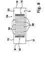
- FIG. 8 shows a further simultaneous analysis unit 34 with a flow cell 35 in plan view a parallel to a waveguide 7 laid section.
- the flow cell 35 has a number of recesses 36, which expediently equidistant between the coupling grid 10 and the decoupling grid 15 spaced and transversely to the propagation direction of are aligned via the coupling grating 10 coupled excitation radiation 18.
- Siultananalysetician 34 are also different, in the recesses 36th introduced sample liquids 19 simultaneously on the evanescently excited radiation 21 examined, here a defined superposition of the different radiation components the evanescently excited radiation 21 is brought about.
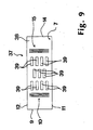
- FIG. 9 shows a further embodiment of a simultaneous analysis unit 37 in a section through a flow cell 38 in plan view of a parallel to the slab waveguide 7 set Cut.
- the flow cell 38 has a number of recesses 39 which are parallel are aligned between the side surfaces 11, 12, but each only one Fraction of the distance between the coupling grating 10 and the decoupling grid 15th extend.
- the length is each Recess 39 about one-fifth of the distance between the coupling grid 10 and the Auskoppelgitter 15.
- the recesses 39 are in three each transverse to the Propagation direction of the coupling grid 10 in the slab waveguide.
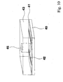
- Fig. 10 shows an example with the recess open at the top.
- a coupling-in grid (42) and a decoupling grid a self-adhesive layer (43) is applied, which consists of polydimethylsiloxane.
- a self-adhesive layer (43) is applied, which consists of polydimethylsiloxane.
- the Layer (43) is a round and upwardly open recess provided with the analyte sample can be filled.
- the flow cells 26, 30, 35 shown in FIGS. 5 and 6, 7, 8 and 9, 38 are also preferably made of the material shown in FIG. 1 and there discussed flow cell 1 produced.
- flow cells 1, 26, 30, 35, 38 in A molding method are the different geometries in a particularly simple manner and arrangements of the recesses 6, 36, 39 producible, so that also relatively complicated geometries or orientations in a single use are still economical.
- all flow cells 1, 26, 30, 35, 38 are made of a virtually fluorescence-free Material are made to evanescent in the flow cells 1, 26, 30, 35, 38 evanescent excited fluorescence radiation with evanescently excited in sample liquid 19 for analysis Radiation 21 to avoid appreciable extent. It is also appropriate that the Flow cells 1, 26, 30, 35, 38, for example, on the end faces 9, 14, the side surfaces 11, 12th and the top surface 4 are radiation-absorbing, to injections of ambient radiation in the layer waveguide 7 to prevent.
- the preparation of the inventive device can be achieved by joining the planar waveguide and the preformed layer (43), optionally with a Adhesion promoters.
- the waveguiding layer may be covered with one determining target molecule can be immobilized, and / or it can be light-absorbing Layers are applied to the waveguide or the preformed layer.
- One Another method of manufacture is to place the layer (43) directly on the waveguiding layer For example, with photosensitive resins and photolithographic methods.
- the devices according to the invention are suitable for the determination of target molecules a luminescence-generating interaction in the analyte sample, as for example especially common in affinity sensor technology.
- the method is in a conventional manner carried out so that one fills the recesses with an analyte sample, then Coupling excitation radiation and then measures the luminescence generated, for example Fluorescent radiation.
- Particularly advantageous for the affinity sensor is that one with a to be determined target molecule immobilized inventive devices optionally under a neutral liquid or the analyte liquid to produce Luminescence for a long time lagem and the measurements later, if necessary, with others collected samples in one go.
- excitation radiation is appropriately used laser light.
- the invention also relates to the use of the inventive device for Determination of target molecules in affinity sensing.
- Another object of the invention is a method for the determination of target molecules, characterized in that (a) in recesses of the device according to the Claims 1 to 10 an analyte sample fills, (b) excitation light on the diffractive element in coupling the waveguide, (c) luminescent molecules in the analyte sample through one evanescent portion of the excitation radiation excites luminescence, and (d) then the generated Luminescence determined.
Landscapes
- Chemical & Material Sciences (AREA)
- Health & Medical Sciences (AREA)
- Physics & Mathematics (AREA)
- Pathology (AREA)
- Life Sciences & Earth Sciences (AREA)
- Analytical Chemistry (AREA)
- Biochemistry (AREA)
- General Health & Medical Sciences (AREA)
- General Physics & Mathematics (AREA)
- Immunology (AREA)
- Chemical Kinetics & Catalysis (AREA)
- Engineering & Computer Science (AREA)
- Nuclear Medicine, Radiotherapy & Molecular Imaging (AREA)
- Plasma & Fusion (AREA)
- Investigating, Analyzing Materials By Fluorescence Or Luminescence (AREA)
- Optical Measuring Cells (AREA)
- Investigating Or Analysing Materials By Optical Means (AREA)
- Optical Integrated Circuits (AREA)
- Inspection Of Paper Currency And Valuable Securities (AREA)
- Preliminary Treatment Of Fibers (AREA)
- Optical Couplings Of Light Guides (AREA)
Priority Applications (1)
| Application Number | Priority Date | Filing Date | Title |
|---|---|---|---|
| EP97954883A EP0938656B1 (de) | 1996-11-18 | 1997-11-18 | Messvorrichtung mit einem planaren optischen wellenleiter |
Applications Claiming Priority (6)
| Application Number | Priority Date | Filing Date | Title |
|---|---|---|---|
| EP96810807 | 1996-11-18 | ||
| EP96810807A EP0843172A1 (de) | 1996-11-18 | 1996-11-18 | Flusszelle sowie Vorrichtung zur Erzeugung evaneszent angeregter Strahlung |
| EP96810808 | 1996-11-18 | ||
| EP96810808A EP0843173A1 (de) | 1996-11-18 | 1996-11-18 | Flusszelle sowie Vorrichtung zur Erzeugung evaneszent angeregter Strahlung |
| EP97954883A EP0938656B1 (de) | 1996-11-18 | 1997-11-18 | Messvorrichtung mit einem planaren optischen wellenleiter |
| PCT/EP1997/006443 WO1998022799A2 (de) | 1996-11-18 | 1997-11-18 | Messvorrichtung und deren verwendung |
Publications (2)
| Publication Number | Publication Date |
|---|---|
| EP0938656A2 EP0938656A2 (de) | 1999-09-01 |
| EP0938656B1 true EP0938656B1 (de) | 2005-10-26 |
Family
ID=26144278
Family Applications (1)
| Application Number | Title | Priority Date | Filing Date |
|---|---|---|---|
| EP97954883A Expired - Lifetime EP0938656B1 (de) | 1996-11-18 | 1997-11-18 | Messvorrichtung mit einem planaren optischen wellenleiter |
Country Status (7)
| Country | Link |
|---|---|
| US (2) | US6198869B1 (https=) |
| EP (1) | EP0938656B1 (https=) |
| JP (1) | JP3748571B2 (https=) |
| AT (1) | ATE308039T1 (https=) |
| AU (1) | AU6291498A (https=) |
| DE (1) | DE59712460D1 (https=) |
| WO (1) | WO1998022799A2 (https=) |
Families Citing this family (77)
| Publication number | Priority date | Publication date | Assignee | Title |
|---|---|---|---|---|
| DE59915078D1 (https=) * | 1998-02-05 | 2009-10-22 | Novartis Ag | |
| FR2783919A1 (fr) * | 1998-09-25 | 2000-03-31 | Suisse Electronique Microtech | Capteur optique integre pour detecter les composants d'un fluide |
| WO2000036442A1 (en) * | 1998-10-29 | 2000-06-22 | Mark Stephen Braiman | Tapered quasi-planar germanium waveguides for mid-ir sensing |
| DE19856041A1 (de) * | 1998-12-04 | 2000-07-13 | Inst Chemo Biosensorik | Verfahren und Vorrichtung zur Durchführung von quantitativen Fluoreszenz markierten Affinitätstests |
| US6225109B1 (en) * | 1999-05-27 | 2001-05-01 | Orchid Biosciences, Inc. | Genetic analysis device |
| US6771376B2 (en) * | 1999-07-05 | 2004-08-03 | Novartis Ag | Sensor platform, apparatus incorporating the platform, and process using the platform |
| KR100883079B1 (ko) | 1999-07-05 | 2009-02-10 | 노파르티스 아게 | 플랫폼, 플랫폼을 가지는 장치, 및 플랫폼을 사용하는 방법 |
| JP5006494B2 (ja) | 1999-08-13 | 2012-08-22 | バイエル・テクノロジー・サービシーズ・ゲゼルシャフト・ミット・ベシュレンクテル・ハフツング | 複数の分析物を測定するためのデバイス及び方法 |
| ATE299589T1 (de) † | 1999-08-20 | 2005-07-15 | Diagnostische Forsch Stiftung | Verfahren zur bestimmung von substanzen mittels der evaneszenzfeldmethode |
| DE19948087B4 (de) * | 1999-10-06 | 2008-04-17 | Evotec Ag | Verfahren zur Herstellung eines Reaktionssubstrats |
| US7167615B1 (en) | 1999-11-05 | 2007-01-23 | Board Of Regents, The University Of Texas System | Resonant waveguide-grating filters and sensors and methods for making and using same |
| US6592733B1 (en) | 1999-11-12 | 2003-07-15 | Motorola, Inc. | Capillary electrophoresis devices incorporating optical waveguides |
| AU2009401A (en) | 1999-12-17 | 2001-06-25 | Zeptosens Ag | Flow cell array and the utilization thereof for multianalyte determination |
| US6580507B2 (en) * | 2000-03-02 | 2003-06-17 | Sd Acquisition Inc. | Single source, single detector chip, multiple-longitudinal channel electromagnetic radiation absorbance and fluorescence monitoring system |
| JP2003533692A (ja) * | 2000-05-06 | 2003-11-11 | ツェプトゼンス アクチエンゲゼルシャフト | 多重分析対象物測定及びその使用のための格子導波路構造 |
| WO2001092870A2 (de) | 2000-06-02 | 2001-12-06 | Zeptosens Ag | Kit und verfahren zur multianalytbestimmung |
| US7158224B2 (en) | 2000-06-25 | 2007-01-02 | Affymetrix, Inc. | Optically active substrates |
| DE10058095C2 (de) * | 2000-11-03 | 2003-12-18 | Fraunhofer Ges Forschung | Vorrichtung zur Bestimmung von Analyten durch Chemilumineszenz |
| EP1405056A1 (de) * | 2001-06-15 | 2004-04-07 | Zeptosens AG | Körper für durchflussküvetten und deren verwendung |
| GB0207944D0 (en) * | 2002-04-05 | 2002-05-15 | Univ Cambridge Tech | Method of detection |
| US20030232427A1 (en) * | 2002-06-18 | 2003-12-18 | Montagu Jean I. | Optically active substrates for examination of biological materials |
| DE10307802A1 (de) * | 2003-02-24 | 2004-09-09 | Advalytix Ag | Analyseverfahren und -Vorrichtung zur Analyse von spezifischen Bindungsreaktionen |
| US7545494B2 (en) * | 2003-07-23 | 2009-06-09 | Bayer Technology Services Gmbh | Analytical system and method for analyzing nonlinear optical signals |
| DE102004039564B4 (de) * | 2004-08-13 | 2006-06-29 | Institut für Lasertechnologien in der Medizin und Meßtechnik an der Universität Ulm | Vorrichtung zum optischen Screening von Oberflächen biologischer Proben in zweidimensionaler Anordnung |
| US7095941B2 (en) * | 2004-10-27 | 2006-08-22 | Schott Corporation | Fused optical fiber optical device system |
| JP2006162538A (ja) * | 2004-12-10 | 2006-06-22 | Seiko Instruments Inc | 微量質量測定装置 |
| GB0501944D0 (en) | 2005-01-31 | 2005-03-09 | Univ Cambridge Tech | Compounds for use in chemical detection and/or quantitation |
| JP4290128B2 (ja) * | 2005-02-25 | 2009-07-01 | キヤノン株式会社 | センサ |
| US20070196863A1 (en) * | 2006-02-17 | 2007-08-23 | Hanson Technologies, Inc. | Prion protein detection |
| US8288157B2 (en) * | 2007-09-12 | 2012-10-16 | Plc Diagnostics, Inc. | Waveguide-based optical scanning systems |
| US8675199B2 (en) * | 2006-03-10 | 2014-03-18 | Plc Diagnostics, Inc. | Waveguide-based detection system with scanning light source |
| US7951583B2 (en) * | 2006-03-10 | 2011-05-31 | Plc Diagnostics, Inc. | Optical scanning system |
| US9528939B2 (en) | 2006-03-10 | 2016-12-27 | Indx Lifecare, Inc. | Waveguide-based optical scanning systems |
| US9976192B2 (en) | 2006-03-10 | 2018-05-22 | Ldip, Llc | Waveguide-based detection system with scanning light source |
| US9423397B2 (en) | 2006-03-10 | 2016-08-23 | Indx Lifecare, Inc. | Waveguide-based detection system with scanning light source |
| US8207509B2 (en) | 2006-09-01 | 2012-06-26 | Pacific Biosciences Of California, Inc. | Substrates, systems and methods for analyzing materials |
| US7639355B2 (en) * | 2007-06-26 | 2009-12-29 | Hewlett-Packard Development Company, L.P. | Electric-field-enhancement structure and detection apparatus using same |
| DE102007033124B4 (de) * | 2007-07-16 | 2012-12-06 | Fraunhofer-Gesellschaft zur Förderung der angewandten Forschung e.V. | Vorrichtung zur optischen Detektion von Substanzen in einem flüssigen oder gasförmigen Medium |
| US7860354B2 (en) * | 2007-11-06 | 2010-12-28 | Kabushiki Kaisha Toshiba | Optical sensor |
| JP2009133836A (ja) * | 2007-11-06 | 2009-06-18 | Toshiba Corp | 光学式センサ |
| EP2110694B1 (en) | 2008-04-18 | 2013-08-14 | Sony DADC Austria AG | Method for manufacturing an optical waveguide, optical waveguide, and sensor arrangement |
| GB2461026B (en) * | 2008-06-16 | 2011-03-09 | Plc Diagnostics Inc | System and method for nucleic acids sequencing by phased synthesis |
| EP2331934B1 (en) | 2008-09-16 | 2020-01-01 | Pacific Biosciences of California, Inc. | Analytic device including a zero mode waveguide substrate |
| JP2010151510A (ja) * | 2008-12-24 | 2010-07-08 | Tdk Corp | 液性測定装置 |
| US9658222B2 (en) | 2009-03-02 | 2017-05-23 | Mbio Diagnostics, Inc. | Planar waveguide based cartridges and associated methods for detecting target analyte |
| US9212995B2 (en) | 2009-03-02 | 2015-12-15 | Mbio Diagnostics, Inc. | System and method for detecting multiple molecules in one assay |
| US8331751B2 (en) * | 2009-03-02 | 2012-12-11 | mBio Diagnositcs, Inc. | Planar optical waveguide with core of low-index-of-refraction interrogation medium |
| US8586347B2 (en) | 2010-09-15 | 2013-11-19 | Mbio Diagnostics, Inc. | System and method for detecting multiple molecules in one assay |
| US8300993B2 (en) * | 2009-03-02 | 2012-10-30 | Mbio Diagnostics, Inc. | Waveguide with integrated lens |
| JP5272965B2 (ja) * | 2009-08-19 | 2013-08-28 | 株式会社島津製作所 | 蛍光検出器 |
| EP3460458B1 (en) | 2010-02-19 | 2021-08-11 | Pacific Biosciences of California, Inc. | A method for nucleic acid sequencing |
| US8994946B2 (en) | 2010-02-19 | 2015-03-31 | Pacific Biosciences Of California, Inc. | Integrated analytical system and method |
| WO2012004735A1 (en) * | 2010-07-09 | 2012-01-12 | Koninklijke Philips Electronics N.V. | Cartridge with large-scale manufacturing design |
| US8750652B2 (en) * | 2010-10-12 | 2014-06-10 | The Board Of Trustees Of The Leland Stanford Junior University | Microfluidic waveguide detector |
| JP5940081B2 (ja) * | 2010-11-19 | 2016-06-29 | ザ リージェンツ オブ ザ ユニヴァーシティ オブ カリフォルニアThe Regents of the University of California | 平面状ハイブリッドオプトフルイディック集積物 |
| IN2014CN01633A (https=) * | 2011-09-06 | 2015-05-08 | Koninkl Philips Nv | |
| WO2013108087A1 (en) * | 2012-01-18 | 2013-07-25 | Jawaharlal Nehru Centre For Advanced Scientific Research | A system and a method to detect hydrogen leakage using nano-crystallised palladium gratings |
| WO2015074001A1 (en) | 2013-11-17 | 2015-05-21 | Quantum-Si Incorporated | Optical system and assay chip for probing, detecting and analyzing molecules |
| US10018566B2 (en) | 2014-02-28 | 2018-07-10 | Ldip, Llc | Partially encapsulated waveguide based sensing chips, systems and methods of use |
| EP2916125A1 (en) * | 2014-03-07 | 2015-09-09 | One Drop Diagnostics Sàrl | Fluorescence-detected assays on microfluidic chips |
| CA2957543A1 (en) | 2014-08-08 | 2016-02-11 | Quantum-Si Incorporated | Optical system and assay chip for probing, detecting and analyzing molecules |
| US10174363B2 (en) | 2015-05-20 | 2019-01-08 | Quantum-Si Incorporated | Methods for nucleic acid sequencing |
| EP4421188A3 (en) | 2014-08-08 | 2024-10-23 | Quantum-Si Incorporated | Integrated device with external light source for probing, detecting, and analyzing molecules |
| EP3471402B1 (en) | 2014-08-08 | 2023-05-31 | Quantum-Si Incorporated | Integrated device for temporal binning of received photons |
| WO2016138427A1 (en) | 2015-02-27 | 2016-09-01 | Indx Lifecare, Inc. | Waveguide-based detection system with scanning light source |
| EP3292220B1 (en) | 2015-05-07 | 2022-07-13 | Pacific Biosciences of California, Inc. | Multiprocessor pipeline architecture |
| CN107850537B (zh) * | 2015-06-30 | 2020-05-19 | Imec 非营利协会 | 辐射载体及其在光学传感器中的使用 |
| KR20180111999A (ko) | 2016-02-17 | 2018-10-11 | 테서렉트 헬스, 인코포레이티드 | 수명 촬상 및 검출 응용을 위한 센서 및 디바이스 |
| CA3047826A1 (en) | 2016-12-22 | 2018-06-28 | Quantum-Si Incorporated | Integrated photodetector with direct binning pixel |
| WO2018160595A2 (en) | 2017-02-28 | 2018-09-07 | The Regents Of The University Of California | Optofluidic analyte detection systems using multi-mode interference waveguides |
| BR112020000826A2 (pt) | 2017-07-24 | 2020-07-21 | Quantum-Si Incorporated | instrumento bio-optoeletrônico maciçamente paralelo portátil |
| CN119364214A (zh) | 2018-06-22 | 2025-01-24 | 宽腾矽公司 | 具有不同检测时间的电荷存储仓的集成光电检测器 |
| US12613187B2 (en) * | 2020-09-18 | 2026-04-28 | Salvus, Llc | Interferometric detection and quantification system and methods of use in chemical processing |
| US11740177B2 (en) | 2020-09-18 | 2023-08-29 | Salvus, Llc | Interferometric detection and quantification system and methods of use in aquatics |
| US11994504B2 (en) | 2020-09-18 | 2024-05-28 | Salvus, Llc | Interferometric detection and quantification system and methods of use in food processing and food supply chain |
| US12399172B2 (en) | 2020-09-18 | 2025-08-26 | Salvus, Llc | Interferometric detection and quantification system and methods of use in healthcare |
| DE102020133924A1 (de) | 2020-12-17 | 2022-06-23 | Carl Zeiss Jena Gmbh | Chiplabor-system mit funktionalisiertem wellenleiter |
Family Cites Families (12)
| Publication number | Priority date | Publication date | Assignee | Title |
|---|---|---|---|---|
| EP0184600B1 (en) * | 1984-12-10 | 1990-03-14 | Prutec Limited | Method for optically ascertaining parameters of species in a liquid analyte |
| SE462408B (sv) * | 1988-11-10 | 1990-06-18 | Pharmacia Ab | Optiskt biosensorsystem utnyttjande ytplasmonresonans foer detektering av en specific biomolekyl, saett att kalibrera sensoranordningen samt saett att korrigera foer baslinjedrift i systemet |
| US5830766A (en) * | 1990-05-23 | 1998-11-03 | Ares-Serono Research & Development Ltd. Partnership | Enhanced signal-to-noise ratio and sensitivity optical immunoassay |
| US5512492A (en) * | 1993-05-18 | 1996-04-30 | University Of Utah Research Foundation | Waveguide immunosensor with coating chemistry providing enhanced sensitivity |
| US5677196A (en) * | 1993-05-18 | 1997-10-14 | University Of Utah Research Foundation | Apparatus and methods for multi-analyte homogeneous fluoro-immunoassays |
| MXPA96005828A (es) | 1994-05-27 | 2005-07-15 | Novartis Ag Tambien Denominada | Proceso para detectar luminescencia excitada evanescentemente. |
| KR19990014709A (ko) * | 1995-05-12 | 1999-02-25 | 한스루돌프하우스 | 센서 플랫폼 및 감쇠 여기된 발광을 이용한 복수 분석물의병렬 검출 방법 |
| WO1997001087A1 (en) * | 1995-06-23 | 1997-01-09 | Novartis Ag | Flow cell |
| US6108463A (en) * | 1996-03-19 | 2000-08-22 | University Of Utah Research Foundation | Lens and associatable flow cell |
| JP3266041B2 (ja) * | 1996-05-22 | 2002-03-18 | 株式会社島津製作所 | 部材接合法及びこの方法により製造した光学測定装置 |
| DE19628002C1 (de) * | 1996-07-11 | 1997-12-18 | Inst Chemo Biosensorik | Vorrichtung und Verfahren zur Durchführung von Fluoreszenzimmunotests |
| US5832165A (en) * | 1996-08-28 | 1998-11-03 | University Of Utah Research Foundation | Composite waveguide for solid phase binding assays |
-
1997
- 1997-11-18 JP JP52320998A patent/JP3748571B2/ja not_active Expired - Fee Related
- 1997-11-18 AT AT97954883T patent/ATE308039T1/de not_active IP Right Cessation
- 1997-11-18 WO PCT/EP1997/006443 patent/WO1998022799A2/de not_active Ceased
- 1997-11-18 DE DE59712460T patent/DE59712460D1/de not_active Expired - Lifetime
- 1997-11-18 AU AU62914/98A patent/AU6291498A/en not_active Abandoned
- 1997-11-18 US US09/308,096 patent/US6198869B1/en not_active Expired - Lifetime
- 1997-11-18 EP EP97954883A patent/EP0938656B1/de not_active Expired - Lifetime
-
2000
- 2000-12-22 US US09/742,391 patent/US6384912B2/en not_active Expired - Lifetime
Also Published As
| Publication number | Publication date |
|---|---|
| US20010001021A1 (en) | 2001-05-10 |
| EP0938656A2 (de) | 1999-09-01 |
| ATE308039T1 (de) | 2005-11-15 |
| DE59712460D1 (de) | 2005-12-01 |
| WO1998022799A3 (de) | 1998-08-20 |
| WO1998022799A2 (de) | 1998-05-28 |
| US6198869B1 (en) | 2001-03-06 |
| AU6291498A (en) | 1998-06-10 |
| JP2001504230A (ja) | 2001-03-27 |
| JP3748571B2 (ja) | 2006-02-22 |
| US6384912B2 (en) | 2002-05-07 |
Similar Documents
| Publication | Publication Date | Title |
|---|---|---|
| EP0938656B1 (de) | Messvorrichtung mit einem planaren optischen wellenleiter | |
| DE10008006C2 (de) | SPR-Sensor und SPR-Sensoranordnung | |
| DE19725050C2 (de) | Anordnung zur Detektion biochemischer oder chemischer Substanzen mittels Fluoreszenzlichtanregung und Verfahren zu deren Herstellung | |
| DE69926230T2 (de) | Optische sensorvorrichtung mit evaneszenter felddetektion | |
| EP1057008B1 (de) | Verfahren und vorrichtung zur lumineszenzmessung | |
| DE19732619C2 (de) | Optische Detektoreinrichtung | |
| DE69231502T2 (de) | Wellenleitersensor | |
| DE69119750T2 (de) | Messzelle für chemische oder biochemische proben | |
| DE68918659T2 (de) | Wellenleitersensor. | |
| DE19628002C1 (de) | Vorrichtung und Verfahren zur Durchführung von Fluoreszenzimmunotests | |
| DE19923820C2 (de) | SPR-Sensor zur gleichzeitigen Erfassung einer Vielzahl von in fluider Form vorliegenden Proben | |
| EP1443320A2 (de) | Sensorchip zur Charakterisierung einer chemischen und/oder biochemischen Substanz | |
| DE19747572C1 (de) | Vorrichtung und Verfahren zur Durchführung von Fluoreszenzimmuntests | |
| EP1264180A2 (de) | Sensorelement zur optischen detektion von chemischen oder biochemischen analyten | |
| DE3832803A1 (de) | Lichtdetektor | |
| EP2598859B1 (de) | Messkassette und messvorrichtung für die detektion von zielmolekülen in einer flüssigen probe durch messung von fluoreszenzemission nach anregung im evaneszenten feld | |
| EP0551456A1 (de) | Optisches verfahren zum selektiven nachweis von spezifischen substanzen in chemischen, biochemischen und biologischen messproben | |
| DE4425462C2 (de) | Spektralphotometer-Zelle | |
| EP0843173A1 (de) | Flusszelle sowie Vorrichtung zur Erzeugung evaneszent angeregter Strahlung | |
| DE102009025072A1 (de) | Verfahren zum Erzeugen eines Bereiches mit erhöhtem Brechungsindex und ein Substrat mit örtlich variablem Brechungsindex | |
| DE10324973B4 (de) | Anordnung und Verfahren zur optischen Detektion von in Proben enthaltenen chemischen, biochemischen Molekülen und/oder Partikeln | |
| EP0843172A1 (de) | Flusszelle sowie Vorrichtung zur Erzeugung evaneszent angeregter Strahlung | |
| WO2004025282A1 (de) | Anordnung zur bestimmung von schichtdickenänderungen | |
| DE102019219949A1 (de) | Substrat | |
| EP2112501A1 (de) | Verfahren und Vorrichtung zur Lumineszenzmessung |
Legal Events
| Date | Code | Title | Description |
|---|---|---|---|
| PUAI | Public reference made under article 153(3) epc to a published international application that has entered the european phase |
Free format text: ORIGINAL CODE: 0009012 |
|
| 17P | Request for examination filed |
Effective date: 19990422 |
|
| AK | Designated contracting states |
Kind code of ref document: A2 Designated state(s): AT BE CH DE DK ES FI FR GB GR IE IT LI LU MC NL PT SE |
|
| RIN1 | Information on inventor provided before grant (corrected) |
Inventor name: BRUNO, ALFREDO EMILIO Inventor name: HELG, ANDREAS Inventor name: OROSZLAN, PETER Inventor name: DUVENECK, GERT LUDWIG Inventor name: PAWLAK, MICHAEL Inventor name: KRAUS, GEROLF |
|
| 17Q | First examination report despatched |
Effective date: 20010525 |
|
| RAP1 | Party data changed (applicant data changed or rights of an application transferred) |
Owner name: NOVARTIS AG |
|
| GRAP | Despatch of communication of intention to grant a patent |
Free format text: ORIGINAL CODE: EPIDOSNIGR1 |
|
| RIC1 | Information provided on ipc code assigned before grant |
Ipc: 7G 01N 21/05 B Ipc: 7G 01N 21/77 A |
|
| RTI1 | Title (correction) |
Free format text: MEASUREMENT DEVICE COMPRISING A PLANAR OPTICAL WAVEGUIDE |
|
| GRAS | Grant fee paid |
Free format text: ORIGINAL CODE: EPIDOSNIGR3 |
|
| GRAA | (expected) grant |
Free format text: ORIGINAL CODE: 0009210 |
|
| AK | Designated contracting states |
Kind code of ref document: B1 Designated state(s): AT BE CH DE DK ES FI FR GB GR IE IT LI LU MC NL PT SE |
|
| PG25 | Lapsed in a contracting state [announced via postgrant information from national office to epo] |
Ref country code: NL Free format text: LAPSE BECAUSE OF FAILURE TO SUBMIT A TRANSLATION OF THE DESCRIPTION OR TO PAY THE FEE WITHIN THE PRESCRIBED TIME-LIMIT Effective date: 20051026 Ref country code: IE Free format text: LAPSE BECAUSE OF FAILURE TO SUBMIT A TRANSLATION OF THE DESCRIPTION OR TO PAY THE FEE WITHIN THE PRESCRIBED TIME-LIMIT Effective date: 20051026 Ref country code: FI Free format text: LAPSE BECAUSE OF FAILURE TO SUBMIT A TRANSLATION OF THE DESCRIPTION OR TO PAY THE FEE WITHIN THE PRESCRIBED TIME-LIMIT Effective date: 20051026 |
|
| REG | Reference to a national code |
Ref country code: GB Ref legal event code: FG4D Free format text: NOT ENGLISH |
|
| REG | Reference to a national code |
Ref country code: CH Ref legal event code: EP |
|
| PG25 | Lapsed in a contracting state [announced via postgrant information from national office to epo] |
Ref country code: AT Free format text: LAPSE BECAUSE OF NON-PAYMENT OF DUE FEES Effective date: 20051118 |
|
| PG25 | Lapsed in a contracting state [announced via postgrant information from national office to epo] |
Ref country code: MC Free format text: LAPSE BECAUSE OF NON-PAYMENT OF DUE FEES Effective date: 20051130 Ref country code: BE Free format text: LAPSE BECAUSE OF NON-PAYMENT OF DUE FEES Effective date: 20051130 |
|
| REG | Reference to a national code |
Ref country code: CH Ref legal event code: NV Representative=s name: SOLVIAS AG Ref country code: IE Ref legal event code: FG4D Free format text: LANGUAGE OF EP DOCUMENT: GERMAN |
|
| REF | Corresponds to: |
Ref document number: 59712460 Country of ref document: DE Date of ref document: 20051201 Kind code of ref document: P |
|
| GBT | Gb: translation of ep patent filed (gb section 77(6)(a)/1977) | ||
| PG25 | Lapsed in a contracting state [announced via postgrant information from national office to epo] |
Ref country code: LU Free format text: LAPSE BECAUSE OF NON-PAYMENT OF DUE FEES Effective date: 20051226 |
|
| PG25 | Lapsed in a contracting state [announced via postgrant information from national office to epo] |
Ref country code: SE Free format text: LAPSE BECAUSE OF FAILURE TO SUBMIT A TRANSLATION OF THE DESCRIPTION OR TO PAY THE FEE WITHIN THE PRESCRIBED TIME-LIMIT Effective date: 20060126 Ref country code: GR Free format text: LAPSE BECAUSE OF FAILURE TO SUBMIT A TRANSLATION OF THE DESCRIPTION OR TO PAY THE FEE WITHIN THE PRESCRIBED TIME-LIMIT Effective date: 20060126 Ref country code: DK Free format text: LAPSE BECAUSE OF FAILURE TO SUBMIT A TRANSLATION OF THE DESCRIPTION OR TO PAY THE FEE WITHIN THE PRESCRIBED TIME-LIMIT Effective date: 20060126 |
|
| PG25 | Lapsed in a contracting state [announced via postgrant information from national office to epo] |
Ref country code: ES Free format text: LAPSE BECAUSE OF FAILURE TO SUBMIT A TRANSLATION OF THE DESCRIPTION OR TO PAY THE FEE WITHIN THE PRESCRIBED TIME-LIMIT Effective date: 20060206 |
|
| PG25 | Lapsed in a contracting state [announced via postgrant information from national office to epo] |
Ref country code: PT Free format text: LAPSE BECAUSE OF FAILURE TO SUBMIT A TRANSLATION OF THE DESCRIPTION OR TO PAY THE FEE WITHIN THE PRESCRIBED TIME-LIMIT Effective date: 20060327 |
|
| NLV1 | Nl: lapsed or annulled due to failure to fulfill the requirements of art. 29p and 29m of the patents act | ||
| REG | Reference to a national code |
Ref country code: IE Ref legal event code: FD4D |
|
| ET | Fr: translation filed | ||
| PLBE | No opposition filed within time limit |
Free format text: ORIGINAL CODE: 0009261 |
|
| STAA | Information on the status of an ep patent application or granted ep patent |
Free format text: STATUS: NO OPPOSITION FILED WITHIN TIME LIMIT |
|
| 26N | No opposition filed |
Effective date: 20060727 |
|
| BERE | Be: lapsed |
Owner name: NOVARTIS A.G. Effective date: 20051130 |
|
| REG | Reference to a national code |
Ref country code: CH Ref legal event code: NV Representative=s name: E. BLUM & CO. AG PATENT- UND MARKENANWAELTE VSP |
|
| REG | Reference to a national code |
Ref country code: FR Ref legal event code: PLFP Year of fee payment: 19 |
|
| PGFP | Annual fee paid to national office [announced via postgrant information from national office to epo] |
Ref country code: DE Payment date: 20151110 Year of fee payment: 19 Ref country code: GB Payment date: 20151118 Year of fee payment: 19 Ref country code: CH Payment date: 20151111 Year of fee payment: 19 Ref country code: IT Payment date: 20151124 Year of fee payment: 19 |
|
| PGFP | Annual fee paid to national office [announced via postgrant information from national office to epo] |
Ref country code: FR Payment date: 20151023 Year of fee payment: 19 |
|
| REG | Reference to a national code |
Ref country code: DE Ref legal event code: R119 Ref document number: 59712460 Country of ref document: DE |
|
| REG | Reference to a national code |
Ref country code: CH Ref legal event code: PL |
|
| GBPC | Gb: european patent ceased through non-payment of renewal fee |
Effective date: 20161118 |
|
| PG25 | Lapsed in a contracting state [announced via postgrant information from national office to epo] |
Ref country code: LI Free format text: LAPSE BECAUSE OF NON-PAYMENT OF DUE FEES Effective date: 20161130 Ref country code: CH Free format text: LAPSE BECAUSE OF NON-PAYMENT OF DUE FEES Effective date: 20161130 |
|
| REG | Reference to a national code |
Ref country code: FR Ref legal event code: ST Effective date: 20170731 |
|
| PG25 | Lapsed in a contracting state [announced via postgrant information from national office to epo] |
Ref country code: IT Free format text: LAPSE BECAUSE OF NON-PAYMENT OF DUE FEES Effective date: 20161118 Ref country code: FR Free format text: LAPSE BECAUSE OF NON-PAYMENT OF DUE FEES Effective date: 20161130 |
|
| PG25 | Lapsed in a contracting state [announced via postgrant information from national office to epo] |
Ref country code: DE Free format text: LAPSE BECAUSE OF NON-PAYMENT OF DUE FEES Effective date: 20170601 Ref country code: GB Free format text: LAPSE BECAUSE OF NON-PAYMENT OF DUE FEES Effective date: 20161118 |