JP4290128B2 - センサ - Google Patents
センサ Download PDFInfo
- Publication number
- JP4290128B2 JP4290128B2 JP2005051998A JP2005051998A JP4290128B2 JP 4290128 B2 JP4290128 B2 JP 4290128B2 JP 2005051998 A JP2005051998 A JP 2005051998A JP 2005051998 A JP2005051998 A JP 2005051998A JP 4290128 B2 JP4290128 B2 JP 4290128B2
- Authority
- JP
- Japan
- Prior art keywords
- light
- photonic crystal
- fluid
- sensor
- detection
- Prior art date
- Legal status (The legal status is an assumption and is not a legal conclusion. Google has not performed a legal analysis and makes no representation as to the accuracy of the status listed.)
- Expired - Fee Related
Links
Images


Classifications
-
- G—PHYSICS
- G01—MEASURING; TESTING
- G01N—INVESTIGATING OR ANALYSING MATERIALS BY DETERMINING THEIR CHEMICAL OR PHYSICAL PROPERTIES
- G01N21/00—Investigating or analysing materials by the use of optical means, i.e. using sub-millimetre waves, infrared, visible or ultraviolet light
- G01N21/75—Systems in which material is subjected to a chemical reaction, the progress or the result of the reaction being investigated
- G01N21/77—Systems in which material is subjected to a chemical reaction, the progress or the result of the reaction being investigated by observing the effect on a chemical indicator
- G01N21/7703—Systems in which material is subjected to a chemical reaction, the progress or the result of the reaction being investigated by observing the effect on a chemical indicator using reagent-clad optical fibres or optical waveguides
- G01N21/774—Systems in which material is subjected to a chemical reaction, the progress or the result of the reaction being investigated by observing the effect on a chemical indicator using reagent-clad optical fibres or optical waveguides the reagent being on a grating or periodic structure
-
- G—PHYSICS
- G01—MEASURING; TESTING
- G01N—INVESTIGATING OR ANALYSING MATERIALS BY DETERMINING THEIR CHEMICAL OR PHYSICAL PROPERTIES
- G01N21/00—Investigating or analysing materials by the use of optical means, i.e. using sub-millimetre waves, infrared, visible or ultraviolet light
- G01N21/17—Systems in which incident light is modified in accordance with the properties of the material investigated
- G01N21/41—Refractivity; Phase-affecting properties, e.g. optical path length
- G01N21/4133—Refractometers, e.g. differential
-
- G—PHYSICS
- G01—MEASURING; TESTING
- G01N—INVESTIGATING OR ANALYSING MATERIALS BY DETERMINING THEIR CHEMICAL OR PHYSICAL PROPERTIES
- G01N33/00—Investigating or analysing materials by specific methods not covered by groups G01N1/00 - G01N31/00
- G01N33/48—Biological material, e.g. blood, urine; Haemocytometers
- G01N33/50—Chemical analysis of biological material, e.g. blood, urine; Testing involving biospecific ligand binding methods; Immunological testing
- G01N33/53—Immunoassay; Biospecific binding assay; Materials therefor
- G01N33/543—Immunoassay; Biospecific binding assay; Materials therefor with an insoluble carrier for immobilising immunochemicals
- G01N33/54366—Apparatus specially adapted for solid-phase testing
- G01N33/54373—Apparatus specially adapted for solid-phase testing involving physiochemical end-point determination, e.g. wave-guides, FETS, gratings
-
- G—PHYSICS
- G01—MEASURING; TESTING
- G01N—INVESTIGATING OR ANALYSING MATERIALS BY DETERMINING THEIR CHEMICAL OR PHYSICAL PROPERTIES
- G01N21/00—Investigating or analysing materials by the use of optical means, i.e. using sub-millimetre waves, infrared, visible or ultraviolet light
- G01N21/75—Systems in which material is subjected to a chemical reaction, the progress or the result of the reaction being investigated
- G01N21/77—Systems in which material is subjected to a chemical reaction, the progress or the result of the reaction being investigated by observing the effect on a chemical indicator
- G01N2021/7769—Measurement method of reaction-produced change in sensor
- G01N2021/7779—Measurement method of reaction-produced change in sensor interferometric
Description
フォトニック結晶は一般に1〜数100μm程度の微小サイズでありながら、環境条件の変化に非常に敏感に反応し、その光学的特性を変化させる。そのため、フォトニック結晶をセンサに応用することにより、微小サイズで高感度なセンサを実現することが可能である。
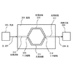
図4に記載のセンサは、第1のフォトニック結晶403と、該第1のフォトニック結晶とは独立した第2のフォトニック結晶404、該第1及び第2のフォトニック結晶に光を入力するための光源405、該第1のフォトニック結晶に接続する第1の流路410と、該第2のフォトニック結晶に接続する第2の流路411、及び該第1および第2のフォトニック結晶を通してそれぞれ出力される光の差分情報を検出する検出部406を備えている。
フォトニック結晶をセンサとして利用する場合、検出を行う物理量(屈折率や物質の濃度)の変化によるフォトニック結晶の光学的特性(透過スペクトルなど)の変化を検出する方法が用いられる。フォトニック結晶表面あるいは近傍の状態が変化(物質吸着や屈折率変化)すると、その光学的性質が変化する。
本発明においては、前記第1及び第2のフォトニック結晶403、404にそれぞれ光を導波するための第1及び第2の光導波路を適用できるが、前述のように独立した光導波路であっても、Y分岐路を備えた光導波路であってもよい。
なお、外乱の影響を2つのフォトニック結晶を用いてキャンセルするために、前記第1及び第2のフォトニック結晶が同一構造であることがより好ましい。
また、センサとして使用する際に、前記第1のフォトニック結晶の表面に、特定物質と選択的に結合する結合物質が担持されていてもよい。
具体的には、流体そのものあるいは流体中に含まれる物質の物理量を検出するためのセンサであって、前記流体を流すための複数の流路が並列に配置され、該流路の一部領域に複数のフォトニック結晶が近接して配置され、該複数のフォトニック結晶に所定の波長範囲の光を照射するための光源と、該光源から前記フォトニック結晶に前記照射光を導波する第1の光導波路と、前記複数のフォトニック結晶から出射される複数の光の複素振幅情報を検出するための光検出部と、前記出射光を該光検出部に導波するための第2の光導波路とを有し、前記フォトニック結晶から出射される光の複素振幅情報の差分から前記流体の所望の物理量を検出するセンサである。
内燃機関の排気系(O2 、CO、NO、NO2 、SO2 、CO等)に用いるガスセンサ、一般家庭で用いる一酸化炭素などの可燃性ガス(メタン、プロパン、ブタン等)警報機に搭載するガスセンサ、呼気中に含まれる有機ガス成分(エタノール、アセトアルデヒド、アンモニア、酢酸等)を検知するセンサ、工場やオフィス内において作業環境を悪化させる物質(ばいじん(粉じん)、遊離ケイ酸、硫黄酸化物(SOx)、窒素酸化物(NOx)、カドミウム、塩素、塩化水素、弗素、鉛、フェノール、アンチモン、ベンゼン、トリクロロエチレン、テトラクロロエチレン、ダイオキシン類、コプラナーPCB、水銀、ホルムアルデヒド、トルエン、キシレン、スチレンモノマー、パラジクロロベンゼン、アクリロニトリル、アセトアルデヒド、塩化ビニルモノマー、クロロホルム、酸化エチレン、1,2−ジクロロエタン、ジクロロメタン、水銀、ダイオキシン類、タルク、テトラクロロエチレン、トリクロロエチレン、ニッケル化合物、砒素、1,3−ブタジエン、浮遊粉じん、ベリリウム、ベンゾ(a)ピレン、ベンゼン、ホルムアルデヒド、マンガン、クロム、アンモニア、メチルメルカプタン、硫化水素、硫化メチル、二硫化メチル、トリメチルアミン、アセトアルデヒド、プロピオンアルデヒド、ノルマルブチルアルデヒド、イソブチルアルデヒド、ノルマルバレルアルデヒド、イソバレルアルデヒド、イソブタノール、酢酸エチル、メチルイソブチルケトン、トルエン、スチレン、キシレン、プロピオン酸、ノルマル酪酸、ノルマル吉草酸、イソ吉草酸等)を検知するセンサ、揮発性環境汚染物質及び地球温暖化原因物質(クロロホルム、四塩化炭素、トリクロロエチレン、1−1−1トリクロロエタン、テトラクロロエチレン、フロン等)を挙げることができる。
(1)環境汚染物質センサ
(2)化学工業、食品工業、薬品工業等の産業での工程・品質管理用、コンビナトリアル合成・コンビナトリアルスクリーニング用センサ
(3)疾病、健康状態診断用センサ
に大別することができる。
前記物理量が流体の屈折率であることが好ましい。
前記物理量が流体中に含まれる物質の濃度であることが好ましい。
前記物理量の変化により、前記出射される光の複素振幅情報が変化することが好ましい。
前記複素振幅情報の変化が振幅変化であることが好ましい。
前記複素振幅情報の差分の検出をマッハツェンダ干渉計を用いた強度検出により行うことが好ましい。
前記複素振幅情報の差分の検出が同期検出によって行われることが好ましい。
実施例1
本実施例は、マッハツェンダ干渉計を用いて本発明のフォトニック結晶と流路を用いたセンサを実施したものである。図4を用いて、本実施例の構成を説明する。
フォトニック結晶403を検出用、フォトニック結晶404を参照用に使用する場合を考える。検出用フォトニック結晶403を含んだ光導波路414と、参照用フォトニック結晶404を含んだ光導波路415の光路長が等しい場合、位相差は0になり干渉光強度は最大になる。ここで流路410と411を用いて、検出用フォトニック結晶に被検出流体、参照用フォトニック結晶に参照用流体を流すと、それぞれの流体の物理量の違いにより、検出用フォトニック結晶と参照用フォトニック結晶の透過光の位相に差分が生じる。その結果、干渉光409の強度が変化する。干渉光強度最大値を基準値として、そこからの強度変化を光検出部406により測定することで、被検出流体と参照用流体の物理量の違いを見積もることができる。
本実施例は、本発明のセンサとロックインアンプを用いて同期検出を行う一形態を示すものである。図7を用いて、本実施例の構成を説明する。
本実施例は本発明のセンサを、流体の屈折率センサとして実施した一形態を示すものである。本実施例では、実施例1あるいは実施例2に示したセンサ構成を用いて、流路に流した流体の屈折率を検出する。
本実施例は本発明のセンサを、特に抗原抗体反応などの特異結合を用いたバイオケミカルセンサとして実施した一形態を示すものである。本実施例では、実施例1あるいは実施例2に示したセンサ構成を用いて、流体中の特定物質の濃度を検出する。図8を用いて、本実施例の構成を説明する。
また、抗原と抗体の配置を逆にした構成、つまり、フォトニック結晶表面に抗原を担持しておいて、そこに抗体を結合させるという構成も可能である。
102 SiO2 層
103 Si基板
104 空孔
201、202、203 光導波路
204 基板
205 光源
206 光検出部
207 光
208 光(干渉光)
209、210 Y分岐路
211 光導波路
401、402 光導波路
403、404 フォトニック結晶
405 光源
406 光検出部
407 基板
408、409 光
410、411 流路
412、413 Y分岐路
414、415 光導波路
501 流路チップ
502 溝(流路)
503 Si層
504 フォトニック結晶
505 光導波路
506 SiO2 層
507 Si基板
601、602 光導波路
603、604 フォトニック結晶
605 光源
606 光検出部
607 基板
608、609 光
610 611 流路
612 位相変調素子
613、614 Y分岐路
615、616 光導波路
701、702 光導波路
703、704 フォトニック結晶
705 光源
706 光検出部
707 基板
708、709 光
710、711 流路
712 Y分岐路部分を含む光スイッチ
713 ロックインアンプ
714 Y分岐路
715、716 光導波路
801 抗原
802 抗原以外の物質
803 抗体
804 フォトニック結晶表面
Claims (9)
- 参照用および検出用の2つの流体を用いて検出用の流体あるいは流体中に含まれる物質の物理量を検出するセンサであって、第1の流体を流す第1の流路と、第2の流体を流す第2の流路と、前記第1の流路に設けられた第1のフォトニック結晶と、前記第2の流路に設けられた第2のフォトニック結晶と、前記第1及び第2のフォトニック結晶に1つの光源から光を照射する光照射手段と、前記第1および第2のフォトニック結晶を通して出力される出力光の複素振幅情報の差分情報から検出用の流体あるいは流体中に含まれる物質の物理量を検出する検出手段を有することを特徴とするセンサ。
- 前記第1及び第2のフォトニック結晶にそれぞれ光を導波するための第1及び第2の光導波路を有することを特徴とする請求項1記載のセンサ。
- 前記第1及び第2のフォトニック結晶にそれぞれ光を導波するためのY分岐型の導波路部を備え、前記光源からの光を分岐して、前記第1及び第2のフォトニック結晶に光を入力することを特徴とする請求項1記載のセンサ。
- 前記第1及び第2のフォトニック結晶を通して出力される光を結合する導波路を有する請求項1から3のいずれか1項に記載のセンサ。
- 前記第1及び第2のフォトニック結晶が同一構造であることを特徴とする請求項1記載のセンサ。
- 前記第1のフォトニック結晶の表面に、特定物質と選択的に結合する結合物質が担持されていることを特徴とする請求項1に記載のセンサ。
- 前記光の差分情報の検出をマッハツェンダ干渉計を用いて行うことを特徴とする請求項1に記載のセンサ。
- 前記第1の光導波路の一部に位相変調素子が設けられていることを特徴とする請求項2に記載のセンサ。
- 前記光の差分情報の検出が同期検出によって行われることを特徴とする請求項1に記載のセンサ。
Priority Applications (2)
| Application Number | Priority Date | Filing Date | Title |
|---|---|---|---|
| JP2005051998A JP4290128B2 (ja) | 2005-02-25 | 2005-02-25 | センサ |
| US11/276,255 US7731902B2 (en) | 2005-02-25 | 2006-02-21 | Photonic crystal and waveguide sensor device |
Applications Claiming Priority (1)
| Application Number | Priority Date | Filing Date | Title |
|---|---|---|---|
| JP2005051998A JP4290128B2 (ja) | 2005-02-25 | 2005-02-25 | センサ |
Publications (3)
| Publication Number | Publication Date |
|---|---|
| JP2006234693A JP2006234693A (ja) | 2006-09-07 |
| JP2006234693A5 JP2006234693A5 (ja) | 2007-02-15 |
| JP4290128B2 true JP4290128B2 (ja) | 2009-07-01 |
Family
ID=37035382
Family Applications (1)
| Application Number | Title | Priority Date | Filing Date |
|---|---|---|---|
| JP2005051998A Expired - Fee Related JP4290128B2 (ja) | 2005-02-25 | 2005-02-25 | センサ |
Country Status (2)
| Country | Link |
|---|---|
| US (1) | US7731902B2 (ja) |
| JP (1) | JP4290128B2 (ja) |
Families Citing this family (27)
| Publication number | Priority date | Publication date | Assignee | Title |
|---|---|---|---|---|
| JP3897688B2 (ja) * | 2002-12-11 | 2007-03-28 | キヤノン株式会社 | 光電融合配線基板 |
| JP4533044B2 (ja) * | 2003-08-27 | 2010-08-25 | キヤノン株式会社 | センサ |
| JP5444711B2 (ja) | 2006-03-17 | 2014-03-19 | 株式会社デンソー | 分析素子およびこれを用いた分析装置 |
| US7809040B2 (en) * | 2007-02-14 | 2010-10-05 | Canon Kabushiki Kaisha | Red surface emitting laser element, image forming device, and image display apparatus |
| KR100860701B1 (ko) | 2007-03-14 | 2008-09-26 | 한양대학교 산학협력단 | 장거리 표면 플라즈몬 이중 금속 광도파로 센서 |
| CA2601836C (en) * | 2007-05-21 | 2017-02-28 | Adam Densmore | Silicon photonic wire waveguide biosensor |
| JP5092161B2 (ja) * | 2007-09-26 | 2012-12-05 | 国立大学法人 新潟大学 | アルコール濃度センサ |
| CN101285820B (zh) * | 2008-04-30 | 2011-07-27 | 中国科学院化学研究所 | 反蛋白石结构膜的用途 |
| JP5356838B2 (ja) * | 2009-01-20 | 2013-12-04 | 株式会社日立製作所 | 自動収尿装置 |
| US9207357B2 (en) | 2009-06-22 | 2015-12-08 | The Trustees Of Princeton University | Non-crystalline materials having complete photonic, electronic, or phononic band gaps |
| US8437965B2 (en) * | 2010-03-01 | 2013-05-07 | Empire Technology Development Llc | Sensing chemicals in aqueous environments |
| JP5659048B2 (ja) * | 2011-03-02 | 2015-01-28 | 株式会社日立製作所 | 光検査方法及びその装置 |
| US11852781B2 (en) | 2011-10-14 | 2023-12-26 | The Trustees Of Princeton University | Narrow-band frequency filters and splitters, photonic sensors, and cavities having pre-selected cavity modes |
| WO2013134463A1 (en) * | 2012-03-08 | 2013-09-12 | Cornell University | Tunable optofluidic apparatus, method and applications |
| CN103076306A (zh) * | 2012-06-11 | 2013-05-01 | 北京邮电大学 | 一种基于级联硅波导与边腔耦合的光子晶体传感器阵列 |
| CN102967584A (zh) * | 2012-10-26 | 2013-03-13 | 中国计量学院 | 基于光子晶体光纤内嵌式干涉仪的挥发性有机物传感方法及装置 |
| JP2014120633A (ja) | 2012-12-17 | 2014-06-30 | Canon Inc | スーパールミネッセントダイオード、スーパールミネッセントダイオードを備えている光干渉断層撮像装置、及びスーパールミネッセントダイオードの制御方法 |
| CN103149176B (zh) * | 2013-02-27 | 2014-10-15 | 大连理工大学 | 一种啁啾二维光子晶体波导集成微流槽多通道折射率传感器 |
| MX2017001808A (es) | 2014-08-08 | 2018-02-08 | Quantum Si Inc | Dispositivo integrado con fuente de luz externa para el sondeo, deteccion y analisis de moleculas. |
| GB2539017B (en) * | 2015-06-03 | 2019-12-18 | Toshiba Res Europe Limited | An optical measuring device |
| WO2017006679A1 (ja) * | 2015-07-07 | 2017-01-12 | 古野電気株式会社 | 測定用チップ、測定装置、および測定方法 |
| EP3676599A1 (en) * | 2017-09-01 | 2020-07-08 | Antelope Dx Bv | Photonic interferometer based sensing |
| US20220244168A1 (en) * | 2019-07-10 | 2022-08-04 | Ams Ag | Photothermal gas detector including an integrated on-chip optical waveguide |
| JP7226192B2 (ja) * | 2019-08-29 | 2023-02-21 | 新東工業株式会社 | 管理方法及び移動端末 |
| JP7243530B2 (ja) | 2019-08-29 | 2023-03-22 | 新東工業株式会社 | 管理方法及び管理装置 |
| US10989535B1 (en) * | 2020-01-31 | 2021-04-27 | Northrop Grumman Systems Corporation | Calibration circuit to mitigate fiber-optic gyroscope (FOG) bias error |
| US20220091086A1 (en) * | 2020-09-18 | 2022-03-24 | Salvus, Llc | Interferometric Detection and Quantification System and Methods of Use in Food Processing and Food Supply Chain |
Family Cites Families (31)
| Publication number | Priority date | Publication date | Assignee | Title |
|---|---|---|---|---|
| US3697185A (en) * | 1970-08-06 | 1972-10-10 | Technicon Instr | Method and apparatus for the time sharing of multiple channel analysis means |
| US4344078A (en) * | 1980-11-06 | 1982-08-10 | Xerox Corporation | Integrated waveguide drop sensor array and method for ink jet printing system |
| US4669878A (en) * | 1984-06-29 | 1987-06-02 | American Monitor Corporation | Automatic monochromator-testing system |
| AU5815886A (en) * | 1985-05-29 | 1986-12-24 | Kurt Tiefenthaler | Optical sensor for selectively determining the presence of substances and the variation of the refraction index in the measured substances |
| US5210590A (en) * | 1992-02-18 | 1993-05-11 | L. T. Industries, Inc. | Rapid scanning spectrographic analyzer |
| US5297224A (en) * | 1992-08-14 | 1994-03-22 | Litton Systems, Inc. | Optically switched sensor array |
| US5345522A (en) * | 1992-09-02 | 1994-09-06 | Hughes Aircraft Company | Reduced noise fiber optic towed array and method of using same |
| JPH07307530A (ja) * | 1994-03-17 | 1995-11-21 | Canon Inc | 偏波変調可能な半導体レーザ |
| US5715173A (en) * | 1994-06-27 | 1998-02-03 | Dainippon Screen Mfg. Co., Ltd. | Concentration controlling method and a substate treating apparatus utilizing same |
| US5485277A (en) * | 1994-07-26 | 1996-01-16 | Physical Optics Corporation | Surface plasmon resonance sensor and methods for the utilization thereof |
| US6081633A (en) * | 1995-11-03 | 2000-06-27 | The United States Of America As Represented By The Secretary Of The Navy | Fiber optic sensor array system with forward coupled topology |
| US5866898A (en) * | 1996-07-12 | 1999-02-02 | The Board Of Trustees Of The Leland Stanford Junior University | Time domain multiplexed amplified sensor array with improved signal to noise ratios |
| US5770472A (en) * | 1996-09-09 | 1998-06-23 | The United States Of America As Represented By The Secretary Of The Army | Method for making monolithically integrated signal processing circuit having active and passive components |
| US6198869B1 (en) * | 1996-11-18 | 2001-03-06 | Novartis Ag | Measuring device and its use |
| US6721053B1 (en) * | 1999-05-19 | 2004-04-13 | Corning Intellisense Corporation | System for high resolution chemical and biological sensing |
| DE10008006C2 (de) * | 2000-02-22 | 2003-10-16 | Graffinity Pharm Design Gmbh | SPR-Sensor und SPR-Sensoranordnung |
| WO2001084197A1 (en) * | 2000-04-28 | 2001-11-08 | Edgelight Biosciences, Inc. | Micro-array evanescent wave fluorescence detection device |
| US6899849B2 (en) * | 2000-07-28 | 2005-05-31 | The Regents Of The University Of California | Integrated sensor |
| JP2003075447A (ja) * | 2001-09-03 | 2003-03-12 | Fuji Photo Film Co Ltd | 表面プラズモン共鳴バイオセンサー用測定チップ |
| US6856733B2 (en) * | 2001-12-07 | 2005-02-15 | Intel Corporation | 1xN fanout waveguide photodetector |
| JP3848210B2 (ja) * | 2002-05-29 | 2006-11-22 | キヤノン株式会社 | 電子回路基板 |
| US7010964B2 (en) * | 2002-10-31 | 2006-03-14 | Nanostream, Inc. | Pressurized microfluidic devices with optical detection regions |
| US7212692B2 (en) * | 2002-11-08 | 2007-05-01 | Ming Yan | Multiple array surface plasmon resonance biosensor |
| JP3897688B2 (ja) * | 2002-12-11 | 2007-03-28 | キヤノン株式会社 | 光電融合配線基板 |
| US6970247B2 (en) * | 2002-12-13 | 2005-11-29 | The United States Of America As Represented By The Secretary Of The Army | Methods and devices for optically recording and imaging representations of interactions of an object with its environment |
| JP4533044B2 (ja) * | 2003-08-27 | 2010-08-25 | キヤノン株式会社 | センサ |
| US7189362B2 (en) * | 2004-03-05 | 2007-03-13 | University Of Alabama In Huntsville | Optical waveguide microcantilever with differential output and associated methods of cantilever sensing |
| US7489846B2 (en) * | 2004-03-11 | 2009-02-10 | Agilent Technologies, Inc. | Photonic crystal sensors |
| US20050201660A1 (en) * | 2004-03-11 | 2005-09-15 | Grot Annette C. | Apparatus for single nanoparticle detection |
| US20060067605A1 (en) * | 2004-09-30 | 2006-03-30 | Laura Wills Mirkarimi | Photonic crystal optical temperature measuring system |
| US7285420B2 (en) * | 2004-11-18 | 2007-10-23 | Corning Incorporated | System and method for self-referencing a sensor in a micron-sized deep flow chamber |
-
2005
- 2005-02-25 JP JP2005051998A patent/JP4290128B2/ja not_active Expired - Fee Related
-
2006
- 2006-02-21 US US11/276,255 patent/US7731902B2/en not_active Expired - Fee Related
Also Published As
| Publication number | Publication date |
|---|---|
| US20060216200A1 (en) | 2006-09-28 |
| JP2006234693A (ja) | 2006-09-07 |
| US7731902B2 (en) | 2010-06-08 |
Similar Documents
| Publication | Publication Date | Title |
|---|---|---|
| JP4290128B2 (ja) | センサ | |
| Uniyal et al. | Recent advances in optical biosensors for sensing applications: a review | |
| Zhang et al. | Applications and developments of on-chip biochemical sensors based on optofluidic photonic crystal cavities | |
| Damborský et al. | Optical biosensors | |
| US11097246B2 (en) | Two-dimensional photonic crystal MicroArray measurement method and apparatus for highly-sensitive label-free multiple analyte sensing, biosensing, and diagnostic assay | |
| Ciminelli et al. | Label-free optical resonant sensors for biochemical applications | |
| Estevez et al. | Integrated optical devices for lab‐on‐a‐chip biosensing applications | |
| Yakovleva et al. | Microfluidic enzyme immunosensors with immobilised protein A and G using chemiluminescence detection | |
| Washburn et al. | Quantitative, label-free detection of five protein biomarkers using multiplexed arrays of silicon photonic microring resonators | |
| Mohammed et al. | Lab-on-a-chip based immunosensor principles and technologies for the detection of cardiac biomarkers: a review | |
| Choi et al. | A 96-well microplate incorporating a replica molded microfluidic network integrated with photonic crystal biosensors for high throughput kinetic biomolecular interaction analysis | |
| Zhu et al. | Opto-fluidic micro-ring resonator for sensitive label-free viral detection | |
| Plowman et al. | Multiple-analyte fluoroimmunoassay using an integrated optical waveguide sensor | |
| US8580200B2 (en) | Method for label-free multiple analyte sensing, biosensing and diagnostic assay | |
| JP4533044B2 (ja) | センサ | |
| JP5230149B2 (ja) | 表面プラズモン共鳴センサおよびバイオチップ | |
| Passaro et al. | Photonic resonant microcavities for chemical and biochemical sensing | |
| Cardenosa-Rubio et al. | Recent advances in environmental and clinical analysis using microring resonator–based sensors | |
| Choi et al. | Comparison of label-free biosensing in microplate, microfluidic, and spot-based affinity capture assays | |
| KR101242138B1 (ko) | 광 바이오 센서, 광 바이오 센서 어레이 및 이를 이용한 바이오 물질의 검출 방법 | |
| US9579621B2 (en) | Method for label-free multiple analyte sensing, biosensing and diagnostic assay | |
| KR100927603B1 (ko) | 표적 바이오 물질 검출 키트 및 표적 바이오 물질 검출방법 | |
| Torrijos-Morán et al. | Integrated optical bimodal waveguide biosensors: Principles and applications | |
| Darwish et al. | Multi-analytic grating coupler biosensor for differential binding analysis | |
| Das et al. | Computational Modeling for Intelligent Surface Plasmon Resonance Sensor Design and Experimental Schemes for Real‐Time Plasmonic Biosensing: A Review |
Legal Events
| Date | Code | Title | Description |
|---|---|---|---|
| A521 | Written amendment |
Free format text: JAPANESE INTERMEDIATE CODE: A523 Effective date: 20061214 |
|
| A621 | Written request for application examination |
Free format text: JAPANESE INTERMEDIATE CODE: A621 Effective date: 20061214 |
|
| A977 | Report on retrieval |
Free format text: JAPANESE INTERMEDIATE CODE: A971007 Effective date: 20090311 |
|
| TRDD | Decision of grant or rejection written | ||
| A01 | Written decision to grant a patent or to grant a registration (utility model) |
Free format text: JAPANESE INTERMEDIATE CODE: A01 Effective date: 20090318 |
|
| A01 | Written decision to grant a patent or to grant a registration (utility model) |
Free format text: JAPANESE INTERMEDIATE CODE: A01 |
|
| A61 | First payment of annual fees (during grant procedure) |
Free format text: JAPANESE INTERMEDIATE CODE: A61 Effective date: 20090331 |
|
| R150 | Certificate of patent or registration of utility model |
Free format text: JAPANESE INTERMEDIATE CODE: R150 |
|
| FPAY | Renewal fee payment (event date is renewal date of database) |
Free format text: PAYMENT UNTIL: 20120410 Year of fee payment: 3 |
|
| FPAY | Renewal fee payment (event date is renewal date of database) |
Free format text: PAYMENT UNTIL: 20130410 Year of fee payment: 4 |
|
| FPAY | Renewal fee payment (event date is renewal date of database) |
Free format text: PAYMENT UNTIL: 20130410 Year of fee payment: 4 |
|
| FPAY | Renewal fee payment (event date is renewal date of database) |
Free format text: PAYMENT UNTIL: 20140410 Year of fee payment: 5 |
|
| LAPS | Cancellation because of no payment of annual fees |