JP4290128B2 - Sensor - Google Patents
Sensor Download PDFInfo
- Publication number
- JP4290128B2 JP4290128B2 JP2005051998A JP2005051998A JP4290128B2 JP 4290128 B2 JP4290128 B2 JP 4290128B2 JP 2005051998 A JP2005051998 A JP 2005051998A JP 2005051998 A JP2005051998 A JP 2005051998A JP 4290128 B2 JP4290128 B2 JP 4290128B2
- Authority
- JP
- Japan
- Prior art keywords
- light
- photonic crystal
- fluid
- sensor
- detection
- Prior art date
- Legal status (The legal status is an assumption and is not a legal conclusion. Google has not performed a legal analysis and makes no representation as to the accuracy of the status listed.)
- Expired - Fee Related
Links
Images


Classifications
-
- G—PHYSICS
- G01—MEASURING; TESTING
- G01N—INVESTIGATING OR ANALYSING MATERIALS BY DETERMINING THEIR CHEMICAL OR PHYSICAL PROPERTIES
- G01N21/00—Investigating or analysing materials by the use of optical means, i.e. using sub-millimetre waves, infrared, visible or ultraviolet light
- G01N21/75—Systems in which material is subjected to a chemical reaction, the progress or the result of the reaction being investigated
- G01N21/77—Systems in which material is subjected to a chemical reaction, the progress or the result of the reaction being investigated by observing the effect on a chemical indicator
- G01N21/7703—Systems in which material is subjected to a chemical reaction, the progress or the result of the reaction being investigated by observing the effect on a chemical indicator using reagent-clad optical fibres or optical waveguides
- G01N21/774—Systems in which material is subjected to a chemical reaction, the progress or the result of the reaction being investigated by observing the effect on a chemical indicator using reagent-clad optical fibres or optical waveguides the reagent being on a grating or periodic structure
-
- G—PHYSICS
- G01—MEASURING; TESTING
- G01N—INVESTIGATING OR ANALYSING MATERIALS BY DETERMINING THEIR CHEMICAL OR PHYSICAL PROPERTIES
- G01N21/00—Investigating or analysing materials by the use of optical means, i.e. using sub-millimetre waves, infrared, visible or ultraviolet light
- G01N21/17—Systems in which incident light is modified in accordance with the properties of the material investigated
- G01N21/41—Refractivity; Phase-affecting properties, e.g. optical path length
- G01N21/4133—Refractometers, e.g. differential
-
- G—PHYSICS
- G01—MEASURING; TESTING
- G01N—INVESTIGATING OR ANALYSING MATERIALS BY DETERMINING THEIR CHEMICAL OR PHYSICAL PROPERTIES
- G01N33/00—Investigating or analysing materials by specific methods not covered by groups G01N1/00 - G01N31/00
- G01N33/48—Biological material, e.g. blood, urine; Haemocytometers
- G01N33/50—Chemical analysis of biological material, e.g. blood, urine; Testing involving biospecific ligand binding methods; Immunological testing
- G01N33/53—Immunoassay; Biospecific binding assay; Materials therefor
- G01N33/543—Immunoassay; Biospecific binding assay; Materials therefor with an insoluble carrier for immobilising immunochemicals
- G01N33/54366—Apparatus specially adapted for solid-phase testing
- G01N33/54373—Apparatus specially adapted for solid-phase testing involving physiochemical end-point determination, e.g. wave-guides, FETS, gratings
-
- G—PHYSICS
- G01—MEASURING; TESTING
- G01N—INVESTIGATING OR ANALYSING MATERIALS BY DETERMINING THEIR CHEMICAL OR PHYSICAL PROPERTIES
- G01N21/00—Investigating or analysing materials by the use of optical means, i.e. using sub-millimetre waves, infrared, visible or ultraviolet light
- G01N21/75—Systems in which material is subjected to a chemical reaction, the progress or the result of the reaction being investigated
- G01N21/77—Systems in which material is subjected to a chemical reaction, the progress or the result of the reaction being investigated by observing the effect on a chemical indicator
- G01N2021/7769—Measurement method of reaction-produced change in sensor
- G01N2021/7779—Measurement method of reaction-produced change in sensor interferometric
Description
本発明は、流路中を流れる流体の屈折率測定や、流体中の標的物質の検出などに用いるセンサに関する。 The present invention relates to a sensor used for measuring a refractive index of a fluid flowing in a flow path, detecting a target substance in the fluid, and the like.
近年、簡便な在宅医療検査や、タンパク質の構造と機能を解明するプロテオミクスを実現させるための手段として、新しい生体解析・検出技術を持った、高性能なバイオチップやセンサ望まれている。例えば、DNAチップ(DNAマイクロアレイ)、表面プラズモン共鳴、多重内部反射法、フォトニック結晶を利用したセンサが提案され、研究・開発が行われている。 In recent years, high-performance biochips and sensors having new biological analysis / detection techniques have been desired as means for realizing simple home medical examinations and proteomics for elucidating protein structures and functions. For example, a sensor using a DNA chip (DNA microarray), surface plasmon resonance, multiple internal reflection method, and photonic crystal has been proposed and researched and developed.
前述のDNAチップやDNAマイクロアレイと呼ばれるものは、DNA分子の分子認識を利用した遺伝子解析法である。DNAマイクロアレイでは、ガラスなどの小さな担体上に遺伝子由来のcDNAあるいはオリゴヌクレオチドを高密度に配置したマイクロアレイ基板を作る。検体から抽出したmRNAサンプル(あるいはcDNA)に蛍光色素を標識し、このサンプルを含んだ溶液の中に先のマイクロアレイを浸すと、DNAプローブとサンプルのハイブリダイゼーションの仕方の違いによってそれぞれのスポットが異なる色に蛍光発色し、この蛍光シグナル強度を分析することによって遺伝子発現を解析する。DNAチップでは、ガラスや半導体の基板表面上に複数種のオリゴヌクレオチドを、それぞれ別々の微小領域に人工合成する。解析の手法はマイクロアレイと同じで、ハイブリダイゼーションと蛍光標識を利用している。DNAチップは米国のAffymetrix社からGene Chipという商標で市販されている。 What is called the above-mentioned DNA chip or DNA microarray is a gene analysis method using molecular recognition of DNA molecules. In a DNA microarray, a microarray substrate is prepared in which gene-derived cDNAs or oligonucleotides are arranged at high density on a small carrier such as glass. When a fluorescent dye is labeled on an mRNA sample (or cDNA) extracted from a specimen and the previous microarray is immersed in a solution containing this sample, each spot differs depending on the method of hybridization between the DNA probe and the sample. The gene expression is analyzed by fluorescently developing the color and analyzing the fluorescence signal intensity. In a DNA chip, a plurality of types of oligonucleotides are artificially synthesized into separate microregions on a glass or semiconductor substrate surface. The analysis method is the same as that of the microarray, and uses hybridization and fluorescent labeling. DNA chips are commercially available from Affymetrix, USA under the trademark Gene Chip.
どちらの手法も幅広く活用されているが、課題もある。その中の一つが蛍光標識が必要である点である。標識の結合の仕方によってDNAハイブリダイゼーションの特異性が損なわれたり、標識化にばらつきが生じたりするために定量性が悪くなる。したがって医療現場では、まだ本当の実用化には至っていないのが現状である。そのため、蛍光標識を必要としない検出法の開発も盛んに行われている。その例が前述の表面プラズモン共鳴、多重内部反射法、フォトニック結晶を利用したものである。これらは全て、光を用いた検出を行うものである。 Both methods are widely used, but there are challenges. One of them is that a fluorescent label is necessary. Depending on how the label is bound, the specificity of DNA hybridization is impaired, and variations in labeling occur, resulting in poor quantitativeness. Therefore, in the medical field, the actual situation is not yet in actual use. Therefore, the development of detection methods that do not require fluorescent labels has been actively conducted. For example, the above-described surface plasmon resonance, multiple internal reflection method, and photonic crystal are used. All of these perform detection using light.
特許文献1は、表面プラズモン共鳴効果を用いた方法であり、抗体が担持された金属表面と、抗原を含有する溶液の接触時の抗原と抗体の結合による、光励起された金属表面の表面プラズモンの共鳴モードの変化を検出光により測定する方法が提案されている。 Patent Document 1 is a method using the surface plasmon resonance effect, which is a method of surface plasmon on a photoexcited metal surface by binding of an antibody to a metal surface on which an antibody is supported and an antigen-antibody when contacting a solution containing the antigen. A method of measuring a change in resonance mode with detection light has been proposed.
また、フォトニック結晶を利用したセンサの例として、非特許文献1が知られている。これは、フォトニック結晶を用いて作製された微小共振器レーザ中に数種類の液体を導入し、屈折率の違いによるレーザ発振波長シフトを観測したものである。 Non-Patent Document 1 is known as an example of a sensor using a photonic crystal. This is one in which several types of liquids were introduced into a microcavity laser fabricated using a photonic crystal, and a laser oscillation wavelength shift due to a difference in refractive index was observed.
本発明におけるフォトニック結晶とは、「ナノテクノロジー大事典(工業調査会)」に記載されている様に、「屈折率が一定の周期で空間的に変化する構造体」のことである。
フォトニック結晶は一般に1〜数100μm程度の微小サイズでありながら、環境条件の変化に非常に敏感に反応し、その光学的特性を変化させる。そのため、フォトニック結晶をセンサに応用することにより、微小サイズで高感度なセンサを実現することが可能である。
The photonic crystal in the present invention is a “structure whose refractive index changes spatially at a constant period” as described in “Encyclopedia of Nanotechnology (Industry Research Committee)”.
Although the photonic crystal is generally a minute size of about 1 to several hundred μm, it reacts very sensitively to changes in environmental conditions and changes its optical characteristics. Therefore, by applying a photonic crystal to a sensor, it is possible to realize a highly sensitive sensor with a small size.
フォトニック結晶の中でも、Si(シリコン)−2次元フォトニック結晶は、半導体微細加工技術を応用して比較的容易に作製することができるため、センサ分野に限らず、様々な分野で盛んに研究が行われている。ここで言うところの2次元フォトニック結晶とは、2次元方向に周期的な屈折率分布を持つ構造体のことである。図1にSOI(Silicon On Insulator)基板上に作製されたSi‐2次元フォトニック結晶の一例を示す。図1(a)は平面図、図1(b)は図1(a)中A−A’直線での断面図である。Si基板103上にSiO2 層102が形成され、さらにその上にSi層101が形成されている。Si層には空孔104が三角格子状に周期的に配列されている。
Among photonic crystals, Si (silicon) -2D photonic crystals can be fabricated relatively easily by applying semiconductor microfabrication technology, so they are actively studied not only in the sensor field but also in various fields. Has been done. The two-dimensional photonic crystal mentioned here is a structure having a periodic refractive index distribution in the two-dimensional direction. FIG. 1 shows an example of a Si-2D photonic crystal fabricated on an SOI (Silicon On Insulator) substrate. 1A is a plan view, and FIG. 1B is a cross-sectional view taken along a line AA ′ in FIG. 1A. A SiO 2 layer 102 is formed on a
また、μ−TAS(Micro Total Analysis System)あるいはLab on Chipと呼ばれる、一度に多様な測定を行うことができる小型化学分析システムも近年注目を集め、盛んに研究が行われている。μ−TASあるいはLab on Chipとは、ガラスなどの小さな基板にポンプ、バルブ、センサなどを集積化した化学分析システムである。その特長として、小型であるため少量のサンプルで測定可能であること、試薬の量を抑えられること、反応時間を短縮できることなどが挙げられる。医療現場や環境測定の分野においてその特長を最大限に発揮できると考えられる。 In addition, a small chemical analysis system called μ-TAS (Micro Total Analysis System) or Lab on Chip that can perform various measurements at once has attracted attention in recent years and has been actively studied. μ-TAS or Lab on Chip is a chemical analysis system in which pumps, valves, sensors, and the like are integrated on a small substrate such as glass. Its features include that it can be measured with a small amount of sample due to its small size, the amount of reagent can be suppressed, and the reaction time can be shortened. It is thought that the feature can be exhibited to the maximum in the medical field and the field of environmental measurement.
前述のSi−2次元フォトニック結晶は平面形状であることから、μ−TASとの融合が比較的容易である。また、平面プロセスで作製されること、微小サイズであることなどから複数のフォトニック結晶や複数の光導波路を用いて容易にシステム化できるという特長も持つ。そのため、Si−2次元フォトニック結晶は、μ−TASを含めた小型で総合的な分析を行えるセンサ構造のプラットフォームとして有望であると考えられる。
しかしながら、フォトニック結晶を利用した従来のセンサは、様々な環境変化に敏感に反応してしまうため、検出しようとしている以外の環境条件の変化(所謂外乱)がある場合にSN比が下がるという課題があった。外乱とは、外から加わる不要な信号のことで、温度変化による屈折率変化、外力や熱膨張による変形、振動、バッファ溶液密度のゆらぎなどが原因で生じる。 However, since the conventional sensor using a photonic crystal reacts sensitively to various environmental changes, the S / N ratio decreases when there is a change in environmental conditions other than the detection (so-called disturbance). was there. A disturbance is an unnecessary signal applied from the outside, and is caused by a change in refractive index due to a temperature change, deformation due to an external force or thermal expansion, vibration, fluctuation of the buffer solution density, and the like.
本発明は、外乱の影響を受けにくいセンサを提供することを目的とする。 An object of this invention is to provide the sensor which is hard to receive the influence of a disturbance.
本発明に係るセンサは、参照用および検出用の2つの流体を用いて検出用の流体あるいは流体中に含まれる物質の物理量を検出するセンサであって、第1の流体を流す第1の流路と、第2の流体を流す第2の流路と、前記第1の流路に設けられた第1のフォトニック結晶と、前記第2の流路に設けられた第2のフォトニック結晶と、前記第1及び第2のフォトニック結晶に1つの光源から光を照射する光照射手段と、前記第1および第2のフォトニック結晶を通して出力される出力光の複素振幅情報の差分情報から検出用の流体あるいは流体中に含まれる物質の物理量を検出する検出手段を有することを特徴とする。 The sensor according to the present invention is a sensor for detecting a physical quantity of a detection fluid or a substance contained in the fluid using two fluids for reference and detection, and the first flow for flowing the first fluid. A channel, a second channel for flowing a second fluid, a first photonic crystal provided in the first channel, and a second photonic crystal provided in the second channel A light irradiating means for irradiating light from one light source to the first and second photonic crystals, and difference information of complex amplitude information of output light output through the first and second photonic crystals. It has a detection means which detects the physical quantity of the substance contained in the fluid or fluid for detection.
本発明のセンサの構成により、外乱の影響を受けにくいセンサを実現することができる。 With the configuration of the sensor of the present invention, it is possible to realize a sensor that is not easily affected by disturbance.
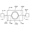
本発明について具体的に図4を用いて説明する。
図4に記載のセンサは、第1のフォトニック結晶403と、該第1のフォトニック結晶とは独立した第2のフォトニック結晶404、該第1及び第2のフォトニック結晶に光を入力するための光源405、該第1のフォトニック結晶に接続する第1の流路410と、該第2のフォトニック結晶に接続する第2の流路411、及び該第1および第2のフォトニック結晶を通してそれぞれ出力される光の差分情報を検出する検出部406を備えている。
The present invention will be specifically described with reference to FIG.
The sensor shown in FIG. 4 inputs light to the first
ここで、複数のフォトニック結晶を用いた外乱低減の原理を説明する。
フォトニック結晶をセンサとして利用する場合、検出を行う物理量(屈折率や物質の濃度)の変化によるフォトニック結晶の光学的特性(透過スペクトルなど)の変化を検出する方法が用いられる。フォトニック結晶表面あるいは近傍の状態が変化(物質吸着や屈折率変化)すると、その光学的性質が変化する。
Here, the principle of disturbance reduction using a plurality of photonic crystals will be described.
When using a photonic crystal as a sensor, a method of detecting a change in optical characteristics (such as a transmission spectrum) of the photonic crystal due to a change in a physical quantity (refractive index or substance concentration) to be detected is used. When the state of the photonic crystal surface or its vicinity changes (substance adsorption or refractive index change), its optical properties change.
図9に、屈折率変化による透過スペクトル波長シフトの模式図を示す。フォトニック結晶近傍の屈折率が増大した場合、一般に透過スペクトルは長波長側にシフトする。このシフト量をΔλ1とする。この屈折率変化量と波長シフト量との間に定量的な関係が成り立てば、透過スペクトルの測定を通して屈折率測定を行うことが可能となる。 FIG. 9 shows a schematic diagram of the transmission spectrum wavelength shift due to the refractive index change. When the refractive index near the photonic crystal increases, the transmission spectrum generally shifts to the longer wavelength side. This shift amount is assumed to be Δλ 1 . If a quantitative relationship is established between the amount of change in refractive index and the amount of wavelength shift, the refractive index can be measured through measurement of the transmission spectrum.
しかし、フォトニック結晶センサは高感度であるがゆえに、検出を意図しない環境変化(所謂外乱)までも検出してしまい、結果としてSN比が下がってしまうという課題がある。 However, since the photonic crystal sensor is highly sensitive, it also detects an environmental change (so-called disturbance) that is not intended for detection, resulting in a problem that the S / N ratio decreases.
例として、温度変化による外乱について説明する。フォトニック結晶の温度が上がると熱膨張により形状が変化し、同時に屈折率も変化する。この2つの効果が重なって、温度上昇とともに透過スペクトルは長波長側にシフトする。このシフト量をΔλ2とすると、透過スペクトルのトータルのシフト量Δλ=Δλ1+Δλ2となり、そこから屈折率変化によるシフト量Δλ1だけを検出することは難しく、結果としてセンサ感度向上の妨げとなる。 As an example, a disturbance due to a temperature change will be described. When the temperature of the photonic crystal rises, the shape changes due to thermal expansion, and the refractive index also changes. These two effects overlap, and the transmission spectrum shifts to the longer wavelength side as the temperature rises. If this shift amount is Δλ 2 , the total shift amount of the transmission spectrum is Δλ = Δλ 1 + Δλ 2 , and it is difficult to detect only the shift amount Δλ 1 due to the change in the refractive index, resulting in hindering the improvement of the sensor sensitivity. Become.
図4に例示しているように、本発明に係るセンサは、外乱そのものを低減するわけではなく、複数のフォトニック結晶を用いてその差分をとることにより外乱の影響をキャンセルする方法を用いる。 As illustrated in FIG. 4, the sensor according to the present invention does not reduce the disturbance itself, but uses a method of canceling the influence of the disturbance by taking the difference using a plurality of photonic crystals.
例えば、同一の構造を持つ2つのフォトニック結晶のうち、1つを検出用、もう1つを参照用とする。検出用フォトニック結晶に検出用流体(例えば、バッファ溶液+たんぱく質)、参照用フォトニック結晶に参照用流体(バッファ溶液)を導入したとする。2つのフォトニック結晶にかかる外乱の影響が共通であれば、2つのフォトニック結晶間の違いはタンパク質の有無だけである。ここで2つのフォトニック結晶の透過スペクトルの差分をとれば、それはタンパク質の有無によってのみ生じたものとなり、外乱の影響をキャンセルした検出が可能となる。 For example, one of two photonic crystals having the same structure is used for detection and the other is used for reference. It is assumed that a detection fluid (for example, a buffer solution + protein) is introduced into the detection photonic crystal, and a reference fluid (buffer solution) is introduced into the reference photonic crystal. If the influence of disturbance on the two photonic crystals is common, the only difference between the two photonic crystals is the presence or absence of protein. Here, if the difference between the transmission spectra of the two photonic crystals is taken, the difference is caused only by the presence or absence of protein, and detection that cancels the influence of disturbance is possible.
なお上記では簡単のため透過スペクトルシフトの場合について説明したが、それ以外の光学的性質(例えば、強度や位相変化)を測定する場合でも考え方は同じである。重要なのは、複数のフォトニック結晶間に生じる差分を測定することにより外乱の影響を低減したセンシングが可能になるという点である。 In the above description, the case of transmission spectrum shift has been described for the sake of simplicity. However, the concept is the same when measuring other optical properties (for example, intensity and phase change). What is important is that sensing that reduces the influence of disturbance is possible by measuring the difference generated between a plurality of photonic crystals.
なお、図4においては、光源は1つとして、その後一旦共通の導波路に光を入力し、Y分岐したのち、それぞれのフォトニック結晶に光を入力しているが、2つの光源を用いて、それぞれのフォトニック結晶に光入力してもよい。 In FIG. 4, the number of light sources is one. Thereafter, light is once input to a common waveguide and then branched into Y, and then light is input to each photonic crystal. However, two light sources are used. The light may be input to each photonic crystal.
また、それぞれのフォトニック結晶を通して出力される光を図4では、再度Y分岐路の導き、光結合させた後光検出部に入力しているが、それぞれのフォトニック結晶を通して出力される光を取り出したあと、光検出部内で結合させてもよい。 In FIG. 4, the light output through each photonic crystal is guided to the Y branch path again and optically coupled, and then input to the light detection unit. However, the light output through each photonic crystal is input. After taking out, you may combine within a photon detection part.
また、前記第1及び第2の流路を独立したもので構成することができる。あるいは、第1の流路403と第2の流路411は、流体が流れるその上流がにおいても完全に独立している必要は無く、それぞれのフォトニック結晶に光導路が接続される箇所で独立していてもよい。即ち、分岐構造をもつ流路を前記第1及び第2の流路に用いることが出来る。
In addition, the first and second flow paths can be configured independently. Alternatively, the
なお、光を用いた検出を行うセンサに、光の干渉効果を利用した構成がしばしば用いられる。干渉型センサの構成方法には、リング型、マイケルソン型、ファブリ・ペロー型、マッハツェンダ型などがあり、目的に応じて使われている。本発明においても様々な型のものを適用できる。 In addition, the structure using the interference effect of light is often used for the sensor which performs the detection using light. There are ring-type, Michelson-type, Fabry-Perot-type, Mach-Zehnder-type, etc., as the configuration method of the interference type sensor, which are used according to the purpose. Various types can also be applied in the present invention.
図2に、Y分岐導波路を用いて構成されたマッハツェンダ干渉計の模式図を示す。光源205から出射された光207は光導波路201を伝搬して第1のY分岐路209で2つの光波に分割され、それぞれ光導波路203と光導波路211を伝搬した後に第2のY分岐路210で1つに合成される。合成された光は光導波路202を伝搬し、光導波路202から出射された光208の複素振幅情報を光検出部206で検出する。例えば、光検出部として光パワーメータを用いれば、合成された光の強度(干渉光強度)を測定することができる。
FIG. 2 shows a schematic diagram of a Mach-Zehnder interferometer configured using a Y-branch waveguide. The light 207 emitted from the light source 205 propagates through the
図3は角振動数の等しい2つの光波が合成された場合の、2つの光波の間の位相差Δψと干渉光強度Iとの関係の一例である。2つの光波の複素振幅をそれぞれA1cos(ψ1−ωt)、A2cos(ψ2−ωt)とすると、位相差Δψがπの偶数倍の場合、I=(A1+A2)2となり、強度が最大となる。一方、πの奇数倍の場合はI=(A1−A2)2となり、強度が最小になる。 FIG. 3 shows an example of the relationship between the phase difference Δψ between the two light waves and the interference light intensity I when two light waves having the same angular frequency are combined. Assuming that the complex amplitudes of the two light waves are A 1 cos (ψ 1 −ωt) and A 2 cos (ψ 2 −ωt), respectively, when the phase difference Δψ is an even multiple of π, I = (A 1 + A 2 ) 2 And the strength is maximized. On the other hand, in the case of an odd multiple of π, I = (A 1 −A 2 ) 2 , and the intensity is minimized.
光導波路203と光導波路211の光路長が等しい場合、位相差は0になり干渉光強度は最大になる。ここで光導波路203と光導波路211どちらかの光導波路の環境に変化が生じ、それによって光路長に変化が生じると光導波路203と光導波路211を伝搬してきた光の位相に差分が生じる。その結果、干渉光強度208が変化する。干渉光強度最大値を基準値として、そこからの強度変化を測定することにより、光導波路203と光導波路211のどちらかに生じた環境の変化量を見積もることができる。
When the optical path lengths of the
なお、本発明において、フォトニック結晶と流路が接続しているとは、光学的に接続可能に両者が配置されていることを意味する。
本発明においては、前記第1及び第2のフォトニック結晶403、404にそれぞれ光を導波するための第1及び第2の光導波路を適用できるが、前述のように独立した光導波路であっても、Y分岐路を備えた光導波路であってもよい。
In the present invention, that the photonic crystal and the flow path are connected means that both are arranged so as to be optically connectable.
In the present invention, the first and second optical waveguides for guiding light can be applied to the first and second
前記第1及び第2のフォトニック結晶403、404を通して出力される光を結合する導波路(414、415)を適用できる。
なお、外乱の影響を2つのフォトニック結晶を用いてキャンセルするために、前記第1及び第2のフォトニック結晶が同一構造であることがより好ましい。
Waveguides (414, 415) for coupling light output through the first and second
In order to cancel the influence of disturbance using two photonic crystals, it is more preferable that the first and second photonic crystals have the same structure.
また、流路の構造やサイズなども2つの流路が同一であることが好ましい。
また、センサとして使用する際に、前記第1のフォトニック結晶の表面に、特定物質と選択的に結合する結合物質が担持されていてもよい。
Moreover, it is preferable that two flow paths are the same also about the structure, size, etc. of a flow path.
In addition, when used as a sensor, a binding substance that selectively binds to a specific substance may be supported on the surface of the first photonic crystal.
本発明のセンサは、複数のフォトニック結晶、光導波路、複数の流路、光源、光検出部によって構成される。
具体的には、流体そのものあるいは流体中に含まれる物質の物理量を検出するためのセンサであって、前記流体を流すための複数の流路が並列に配置され、該流路の一部領域に複数のフォトニック結晶が近接して配置され、該複数のフォトニック結晶に所定の波長範囲の光を照射するための光源と、該光源から前記フォトニック結晶に前記照射光を導波する第1の光導波路と、前記複数のフォトニック結晶から出射される複数の光の複素振幅情報を検出するための光検出部と、前記出射光を該光検出部に導波するための第2の光導波路とを有し、前記フォトニック結晶から出射される光の複素振幅情報の差分から前記流体の所望の物理量を検出するセンサである。
The sensor of the present invention includes a plurality of photonic crystals, an optical waveguide, a plurality of flow paths, a light source, and a light detection unit.
Specifically, it is a sensor for detecting the physical quantity of the fluid itself or the substance contained in the fluid, and a plurality of flow paths for flowing the fluid are arranged in parallel, and a partial region of the flow path A plurality of photonic crystals are arranged close to each other, a light source for irradiating the plurality of photonic crystals with light in a predetermined wavelength range, and a first light that guides the irradiation light from the light source to the photonic crystal. An optical waveguide, a light detection unit for detecting complex amplitude information of a plurality of lights emitted from the plurality of photonic crystals, and a second light guide for guiding the emitted light to the light detection unit A sensor that detects a desired physical quantity of the fluid from a difference in complex amplitude information of light emitted from the photonic crystal.
複数の流路は、流路ごとに異なる流体を流すことができるような構成を持ち、流路とフォトニック結晶を組み合わせることにより、各々のフォトニック結晶に選択的に流体を流すことができる。 The plurality of flow paths have a configuration that allows different fluids to flow for each flow path. By combining the flow paths and the photonic crystals, the fluid can be selectively flowed to each photonic crystal.
本発明における流路とは、基板表面もしくは内部に形成された溝あるいは孔によって構成される。流路のサイズは、本発明中のフォトニック結晶を配置可能な大きさであれば特に制限は無いが、μ−TASなどで用いられている層流を利用した流体制御技術を考慮するならば、およそ1〜数100μmの幅が適当である。流路の材質としては、流体に耐性のある材質であれば何でも可能だが、具体的にはPMMA(polymethylmethacrylate)やPDMS(polydimethylsiloxane)やガラスなどが挙げられる。 The flow path in the present invention is constituted by a groove or a hole formed on the surface or inside of the substrate. The size of the flow path is not particularly limited as long as the photonic crystal in the present invention can be arranged, but if a fluid control technique using a laminar flow used in μ-TAS is considered. A width of about 1 to several 100 μm is appropriate. Any material can be used as the material of the flow path as long as it is resistant to fluid, and specific examples include PMMA (polymethylmethacrylate), PDMS (polydimethylsiloxane), and glass.
フォトニック結晶は、流体を流す流路内あるいはその近傍に配置される。ここで言う近傍とは、光電磁場が影響を受ける範囲であり、その範囲は光波長に依存し、概ね波長オーダーである。例えば光波長を1.5μmとすると、その範囲は0.5〜10μm程度である。 The photonic crystal is disposed in or near the flow path through which the fluid flows. The vicinity mentioned here is a range in which the photoelectric magnetic field is affected, and the range depends on the light wavelength and is generally in the wavelength order. For example, when the light wavelength is 1.5 μm, the range is about 0.5 to 10 μm.
フォトニック結晶の構造は、流路中に配置可能なものであれば特に制限は無い。例えば、先に示した三角格子状に空孔が並べられた構造の他に、正方格子状に空孔が配列されたものや、円柱が周期的に配列された構造などが挙げられる。 The structure of the photonic crystal is not particularly limited as long as it can be arranged in the flow path. For example, in addition to the structure in which holes are arranged in a triangular lattice shape as described above, a structure in which holes are arranged in a square lattice shape, a structure in which cylinders are periodically arranged, and the like can be given.
光検出部では、フォトニック結晶から出射される光の複素振幅情報を検出する。出射光の例として透過光、発光、反射光が挙げられる。フォトニック結晶近傍の物理量が変化することにより、出射光が変調を受ける。例えば、光強度の増減や位相の変化、スペクトル形状の変化などが挙げられる。 The light detection unit detects complex amplitude information of light emitted from the photonic crystal. Examples of the emitted light include transmitted light, emitted light, and reflected light. As the physical quantity in the vicinity of the photonic crystal changes, the emitted light is modulated. For example, increase / decrease of light intensity, change of phase, change of spectrum shape, and the like can be mentioned.
複数のフォトニック結晶のうち、少なくとも1つのフォトニック結晶を参照用として用いる。検出用フォトニック結晶と参照用フォトニック結晶は同じ構造を持ったものでも良いし、異なる構造を持ったものでも良い。また、検出用と参照用の用途は固定されたものではなく、測定用途ごとに入れ替わっても良い。 Of the plurality of photonic crystals, at least one photonic crystal is used for reference. The detection photonic crystal and the reference photonic crystal may have the same structure, or may have different structures. Further, the use for detection and the reference are not fixed, and may be switched for each measurement use.
検出用フォトニック結晶近傍と参照用フォトニック結晶近傍の物理量の違いによる、出射光の複素振幅情報の差分を検出する手段を有する。例として、各々の透過光強度を検出器で測定し、電気的に信号処理を行うものや、透過光を合成した干渉光強度を測定するものなどが挙げられる。 Means for detecting a difference in complex amplitude information of emitted light due to a difference in physical quantity between the vicinity of the detection photonic crystal and the vicinity of the reference photonic crystal. Examples include those in which each transmitted light intensity is measured by a detector to electrically perform signal processing, and those in which interference light intensity obtained by combining transmitted light is measured.
本発明における流体には、気体性流体と液体性流体が含まれる。本発明のセンサでは、流体そのものの物理量や、流体中に混合あるいは溶解された形で存在する標的物質の種類や濃度を検出することができる。 The fluid in the present invention includes a gaseous fluid and a liquid fluid. The sensor of the present invention can detect the physical quantity of the fluid itself and the type and concentration of the target substance present in a mixed or dissolved form in the fluid.
本発明のセンサにより気体性流体を検出する例として以下のものが挙げられる。
内燃機関の排気系(O2 、CO、NO、NO2 、SO2 、CO等)に用いるガスセンサ、一般家庭で用いる一酸化炭素などの可燃性ガス(メタン、プロパン、ブタン等)警報機に搭載するガスセンサ、呼気中に含まれる有機ガス成分(エタノール、アセトアルデヒド、アンモニア、酢酸等)を検知するセンサ、工場やオフィス内において作業環境を悪化させる物質(ばいじん(粉じん)、遊離ケイ酸、硫黄酸化物(SOx)、窒素酸化物(NOx)、カドミウム、塩素、塩化水素、弗素、鉛、フェノール、アンチモン、ベンゼン、トリクロロエチレン、テトラクロロエチレン、ダイオキシン類、コプラナーPCB、水銀、ホルムアルデヒド、トルエン、キシレン、スチレンモノマー、パラジクロロベンゼン、アクリロニトリル、アセトアルデヒド、塩化ビニルモノマー、クロロホルム、酸化エチレン、1,2−ジクロロエタン、ジクロロメタン、水銀、ダイオキシン類、タルク、テトラクロロエチレン、トリクロロエチレン、ニッケル化合物、砒素、1,3−ブタジエン、浮遊粉じん、ベリリウム、ベンゾ(a)ピレン、ベンゼン、ホルムアルデヒド、マンガン、クロム、アンモニア、メチルメルカプタン、硫化水素、硫化メチル、二硫化メチル、トリメチルアミン、アセトアルデヒド、プロピオンアルデヒド、ノルマルブチルアルデヒド、イソブチルアルデヒド、ノルマルバレルアルデヒド、イソバレルアルデヒド、イソブタノール、酢酸エチル、メチルイソブチルケトン、トルエン、スチレン、キシレン、プロピオン酸、ノルマル酪酸、ノルマル吉草酸、イソ吉草酸等)を検知するセンサ、揮発性環境汚染物質及び地球温暖化原因物質(クロロホルム、四塩化炭素、トリクロロエチレン、1−1−1トリクロロエタン、テトラクロロエチレン、フロン等)を挙げることができる。
Examples of detecting a gaseous fluid by the sensor of the present invention include the following.
Installed in gas sensors used for exhaust systems of internal combustion engines (O 2 , CO, NO, NO 2 , SO 2 , CO, etc.) and flammable gas (methane, propane, butane, etc.) alarms such as carbon monoxide used in general households Gas sensors, sensors that detect organic gas components (ethanol, acetaldehyde, ammonia, acetic acid, etc.) contained in exhaled breath, substances that deteriorate the working environment in factories and offices (dust, dust, free silicic acid, sulfur oxides) (SOx), nitrogen oxide (NOx), cadmium, chlorine, hydrogen chloride, fluorine, lead, phenol, antimony, benzene, trichloroethylene, tetrachloroethylene, dioxins, coplanar PCB, mercury, formaldehyde, toluene, xylene, styrene monomer, paradi Chlorobenzene, acrylonitrile, acetaldehyde , Vinyl chloride monomer, chloroform, ethylene oxide, 1,2-dichloroethane, dichloromethane, mercury, dioxins, talc, tetrachloroethylene, trichloroethylene, nickel compounds, arsenic, 1,3-butadiene, suspended dust, beryllium, benzo (a) Pyrene, benzene, formaldehyde, manganese, chromium, ammonia, methyl mercaptan, hydrogen sulfide, methyl sulfide, methyl disulfide, trimethylamine, acetaldehyde, propionaldehyde, normal butyraldehyde, isobutyraldehyde, normal valeraldehyde, isovaleraldehyde, isobutanol, Detects ethyl acetate, methyl isobutyl ketone, toluene, styrene, xylene, propionic acid, normal butyric acid, normal valeric acid, isovaleric acid, etc.) That sensor, the volatile environmental pollutants and greenhouse causative agent (chloroform, carbon tetrachloride, trichlorethylene, 1-1-1 trichloroethane, tetrachlorethylene, Freon, etc.) can be mentioned.
本発明のセンサにより液体性流体を検出する例として以下のものが挙げられる。
(1)環境汚染物質センサ
(2)化学工業、食品工業、薬品工業等の産業での工程・品質管理用、コンビナトリアル合成・コンビナトリアルスクリーニング用センサ
(3)疾病、健康状態診断用センサ
に大別することができる。
Examples of detecting a liquid fluid by the sensor of the present invention include the following.
(1) Sensors for environmental pollutants (2) Sensors for process / quality control in industries such as chemical industry, food industry, and pharmaceutical industry, sensors for combinatorial synthesis / combinatorial screening (3) Sensors for diagnosis of diseases and health conditions be able to.
(1)本発明のセンサが、環境汚染物質センサとして用いられる形態としては、河川・湖沼・海水の水質分析センサ(カドミウム、シアン化合物、有機燐化合物、鉛、六価クロム、砒素、総水銀、アルキル水銀、PCB、トリクロロエチレン、テトラクロロエチレン、ジクロロメタン、四塩化炭素、1,2−ジクロロエタン、1,1−ジクロロエチレン、シス1,2−ジクロロエチレン、1,1,1−トリクロロエタン、1,1,2−トリクロロエタン、1,3−ジクロロプロペン、チウラム、シマジン、チオベンカルブ、ベンゼン、セレン等)、農林業排水等における農薬分析センサ(イソプロチオラン、イプロジオン、エトリジアゾール、オキシン銅(有機銅)、キャプタン、クロロタロニル、クロロネブ、アセフェート、イソキサチオン、ダイアジノン、ピリダフェンチオン、フェニトロチオン(MEP)、アシュラム、ナプロパミド、ブタミホス、ベンスリド(SAP)、メコプロッサ等)、環境ホルモン分析センサ(4−オクチルフェノール、ノニルフェノール、フタル酸ジ−2−エチルヘキシル、フタル酸ブチルベンジル、フタル酸ジ−n−ブチル、フタル酸ジシクロヘキシル、フタル酸ジエチル、アジビン酸ジ−2−エチルヘキシル、ビスフェノールA、スチレンモノマー、ダイオキシン類、ポリ塩化ビフェニール類(PCB)、ポリ臭化ビフェニール類(PBB)、ヘキサクロロベンゼン(HCB)、ペンタクロロフェノール(PCP)、2,4,5−トリクロロフェノキシ酢酸、2,4−ジクロロフェノキシ酢酸、アミトロール、アトラジン、アラクロール、ヘキサクロロシクロヘキサン、クロルデン、オキシクロルデン)等が挙げられる。 (1) The sensor of the present invention can be used as an environmental pollutant sensor in water, water and water quality analysis sensors (cadmium, cyanide, organophosphorus compounds, lead, hexavalent chromium, arsenic, total mercury, Alkylmercury, PCB, trichloroethylene, tetrachloroethylene, dichloromethane, carbon tetrachloride, 1,2-dichloroethane, 1,1-dichloroethylene, cis 1,2-dichloroethylene, 1,1,1-trichloroethane, 1,1,2-trichloroethane, 1,3-dichloropropene, thiuram, simazine, thiobencarb, benzene, selenium, etc., agrochemical analysis sensors (isoprothiolane, iprodione, etridiazole, oxine copper (organic copper), captan, chlorothalonil, chloronebu, acephate, isoxathio) , Diazinon, pyridafenthion, fenitrothion (MEP), ashram, napropamide, butamifos, bensulide (SAP), mecoprosa, etc., environmental hormone analysis sensors (4-octylphenol, nonylphenol, di-2-ethylhexyl phthalate, butylbenzyl phthalate, phthalate) Di-n-butyl acid, dicyclohexyl phthalate, diethyl phthalate, di-2-ethylhexyl adipate, bisphenol A, styrene monomer, dioxins, polychlorinated biphenyls (PCB), polybrominated biphenyls (PBB), hexa Chlorobenzene (HCB), pentachlorophenol (PCP), 2,4,5-trichlorophenoxyacetic acid, 2,4-dichlorophenoxyacetic acid, amitrole, atrazine, alachlor, f Sa chloro cyclohexane, chlordane, and oxy chlordane), and the like.
また、本発明のセンサを用いて土壌や固形廃棄物中の環境汚染物質を標的物質として検出する場合には前記環境汚染物質を土壌或いは固形廃棄物から液性媒体により抽出することにより、場合によってはフィルター等で固形成分を除去した試料を、液体性流体として本発明のセンサにより検出することができる。 In addition, when detecting environmental pollutants in soil or solid waste as a target substance using the sensor of the present invention, by extracting the environmental pollutants from soil or solid waste with a liquid medium, depending on the case. The sample from which the solid component has been removed by a filter or the like can be detected as a liquid fluid by the sensor of the present invention.
(2)本発明のセンサが、化学工業、食品工業、薬品工業等の産業で利用されるセンサの形態としては、食品センサとしては原料のアレルゲン検査、出荷時の安全性試験(食中毒微生物・毒素等)等に用いるセンサとしてであり、化学工業や薬品工業においては、大量のライブラリ候補物質或いは組み合わせ合成反応から所望の物質を選択するコンビナトリアル合成・コンビナトリアルスクリーニング用センサとして用いることができる。 (2) The sensor of the present invention is used in the chemical industry, the food industry, the pharmaceutical industry, etc., as a food sensor. As a food sensor, allergen inspection of raw materials, safety test at the time of shipment (food poisoning microorganisms / toxins In the chemical industry and the pharmaceutical industry, it can be used as a sensor for combinatorial synthesis / combinatorial screening that selects a desired substance from a large number of library candidate substances or combinatorial synthesis reactions.
特に薬品工業における創薬分野では、近年タンパク質或いはペプチド間の相互作用、遺伝子と転写因子のようなタンパク質との相互作用が解明されつつあり、それらがタンパク製剤や遺伝子製剤として応用され始めており、特定のDNAやタンパク質或いはペプチドを結合物質として本発明の固体部分に固定化しておき、膨大なライブラリ中から前記結合物質に特異的に結合する標的物質としてのDNAやタンパク質、ペプチドあるいは化学合成化合物を検知し、有用な薬理作用を有する標的物質をスクリーニングすることが可能である。 In particular, in the drug discovery field in the pharmaceutical industry, interactions between proteins or peptides and interactions between genes and proteins such as transcription factors are being elucidated in recent years, and these have begun to be applied as protein preparations and gene preparations. DNA, protein, or peptide is immobilized on the solid part of the present invention as a binding substance, and DNA, protein, peptide, or chemically synthesized compound as a target substance that specifically binds to the binding substance is detected from a huge library. Thus, it is possible to screen for a target substance having a useful pharmacological action.
(3)本発明のセンサが、疾病、健康状態診断用センサとして用いられる一形態としては、被験者の血液、尿、唾液、リンパ液、等の体液中、或いは被験者の患部細胞より液体抽出した溶液に含まれる疾病マーカーと呼ばれるタンパク質、糖タンパク質、リポタンパク質、ペプチド或いはその複合体を標的物質とし、これらに特異的な抗体を結合物質として本発明のセンサにおける固体部分の空孔像側の表面に固定化した後に、前記標的物質を流路を通して導入し、特異的結合を進行せしめることにより検出を行う形態がある。この場合、血液中の血球成分やその他の体液中の着色成分が検出の妨げとなる場合には予めフィルター等で除去しておくことが望ましい。 (3) As a form in which the sensor of the present invention is used as a sensor for diagnosing illness and health condition, in a body fluid such as blood, urine, saliva, lymph, etc. of a subject, or a liquid extracted from a diseased cell of a subject Proteins, glycoproteins, lipoproteins, peptides or complexes thereof, which are included as disease markers, are used as target substances, and antibodies specific to these are immobilized on the surface of the solid portion in the sensor of the present invention as a binding substance. There is a form in which detection is performed by introducing the target substance through a flow path after the formation of the target substance and allowing specific binding to proceed. In this case, when blood cell components in blood or other colored components in body fluids hinder detection, it is desirable to remove them with a filter or the like in advance.
以下に本発明のセンサの好ましい実施態様を示す。
前記物理量が流体の屈折率であることが好ましい。
前記物理量が流体中に含まれる物質の濃度であることが好ましい。
Preferred embodiments of the sensor of the present invention are shown below.
The physical quantity is preferably the refractive index of the fluid.
The physical quantity is preferably a concentration of a substance contained in the fluid.
前記フォトニック結晶の表面に、特定物質と選択的に結合する結合物質が担持されていることが好ましい。
前記物理量の変化により、前記出射される光の複素振幅情報が変化することが好ましい。
It is preferable that a binding substance that selectively binds to a specific substance is supported on the surface of the photonic crystal.
It is preferable that the complex amplitude information of the emitted light changes due to the change in the physical quantity.
前記複素振幅情報の変化が位相変化であることが好ましい。
前記複素振幅情報の変化が振幅変化であることが好ましい。
前記複素振幅情報の差分の検出をマッハツェンダ干渉計を用いた強度検出により行うことが好ましい。
It is preferable that the change of the complex amplitude information is a phase change.
It is preferable that the change of the complex amplitude information is an amplitude change.
It is preferable that the difference of the complex amplitude information is detected by intensity detection using a Mach-Zehnder interferometer.
前記光導波路の一部に、照射光または出射光の位相を所定量変化させる位相変調素子が配置されていることが好ましい。
前記複素振幅情報の差分の検出が同期検出によって行われることが好ましい。
It is preferable that a phase modulation element for changing the phase of the irradiation light or the outgoing light by a predetermined amount is disposed in a part of the optical waveguide.
It is preferable that the difference of the complex amplitude information is detected by synchronous detection.
前記流路が溝や孔を有する素子を、前記フォトニック結晶を含む面上に配置することによって構成されることが好ましい。 It is preferable that the flow path is configured by disposing an element having a groove or a hole on a surface including the photonic crystal.
以下、実施例を示し本発明をさらに具体的に説明する。
実施例1
本実施例は、マッハツェンダ干渉計を用いて本発明のフォトニック結晶と流路を用いたセンサを実施したものである。図4を用いて、本実施例の構成を説明する。
Hereinafter, the present invention will be described more specifically with reference to examples.
Example 1
In this embodiment, a sensor using a photonic crystal and a flow path according to the present invention is implemented using a Mach-Zehnder interferometer. The configuration of this embodiment will be described with reference to FIG.
Y分岐導波路を用いて構成されたマッハツェンダ干渉計上に2つのフォトニック結晶が配置されている。光源405から光導波路401に照射された光408は、第1のY分岐路412で2つの光波に分割され、分割された光はそれぞれ第1のフォトニック結晶403と光導波路414、第2のフォトニック結晶404と光導波路415を透過する。その後、第2のY分岐路413で1つに合成され、光導波路402から出射された光409の強度を光検出部406で検出する。すなわち、各フォトニック結晶はそれぞれ別個の光導波路に接続され、並列に配置されている。
Two photonic crystals are arranged on a Mach-Zehnder interferometer configured using a Y-branch waveguide. The light 408 emitted from the light source 405 to the
図5(a)に図4中のB−B’断面図の模式図を、図5(b)にその一部を拡大した模式図を示す。流路チップ501に溝502が形成されており、Si層503上に配置されることにより流路を形成する。流路の形状にはいくつかのものが考えられる。図5(b)のようにフォトニック結晶表面をなぞるように流体が流れるタイプの流路や、図5(c)のようにフォトニック結晶上部および下部に溝が形成され、フォトニック結晶中の空孔を流体が通り抜けるような構成も挙げられる。
FIG. 5A shows a schematic diagram of a cross-sectional view along B-B ′ in FIG. 4, and FIG. 5B shows a schematic diagram partially enlarged. A
本実施例においては、異なるフォトニック結晶からの透過光の位相差を検出する。以下その原理について説明する。
フォトニック結晶403を検出用、フォトニック結晶404を参照用に使用する場合を考える。検出用フォトニック結晶403を含んだ光導波路414と、参照用フォトニック結晶404を含んだ光導波路415の光路長が等しい場合、位相差は0になり干渉光強度は最大になる。ここで流路410と411を用いて、検出用フォトニック結晶に被検出流体、参照用フォトニック結晶に参照用流体を流すと、それぞれの流体の物理量の違いにより、検出用フォトニック結晶と参照用フォトニック結晶の透過光の位相に差分が生じる。その結果、干渉光409の強度が変化する。干渉光強度最大値を基準値として、そこからの強度変化を光検出部406により測定することで、被検出流体と参照用流体の物理量の違いを見積もることができる。
In this embodiment, the phase difference of transmitted light from different photonic crystals is detected. The principle will be described below.
Consider a case where the
各々のフォトニック結晶からの透過光を別々に測定して差分をとるのではなく、マッハツェンダ干渉計を構成することの効果として、光源や光検出部や電気回路が少数で済むことによって低コスト化、小型化が可能になることなどが挙げられる。 Rather than measuring the transmitted light from each photonic crystal separately and taking the difference, the effect of constructing a Mach-Zehnder interferometer is to reduce costs by reducing the number of light sources, photodetectors, and electrical circuits. It is possible to reduce the size.
また、図6のように、分岐した導波路のうちどちらか一方に、光の位相を所定量変化させる機能を持つ位相変調素子612を配置した構成も可能である。例えば、光の位相をπだけずらす素子を配置することにより、前述の基準値を干渉光強度最小値にすることができる。それ以外にも、位相のずれを制御することで任意の強度を基準値にすることが可能である。位相変調は、フォトニック結晶への入射光に対して行ってもよいし出射光に対して行ってもよい。
Further, as shown in FIG. 6, a configuration in which a
外乱の影響を防止するために、恒温装置を備える場合、例えば大型化や高コスト化してしまうが、本実施例で示した構成を用いることにより簡便な構成で、外乱をキャンセルすることができる。 In order to prevent the influence of disturbance, when a thermostat is provided, for example, the size and cost are increased. However, the disturbance can be canceled with a simple configuration by using the configuration shown in this embodiment.
実施例2
本実施例は、本発明のセンサとロックインアンプを用いて同期検出を行う一形態を示すものである。図7を用いて、本実施例の構成を説明する。
Example 2
The present embodiment shows an embodiment in which synchronization detection is performed using the sensor of the present invention and a lock-in amplifier. The configuration of this embodiment will be described with reference to FIG.
本実施例の構成では、実施例1と同様にマッハツェンダ干渉計を使用するが、差分の検出方法に干渉光の強度測定ではなく同期検出を用いるところに違いがある。同期検出はノイズ除去のためにしばしば用いられる手法である。第1のY分岐部分に光スイッチ712を配置し、その光スイッチで入射光708に変調を与える。フォトニック結晶703と704を透過した光を第2のY分岐路714で合成し、光709を光検出部706で検出し、検出された信号のうち入射光の変調に同期する信号だけをロックインアンプ713を用いて検出する。光スイッチには光チョッパーやMEMSスイッチなどが使用できる。
In the configuration of the present embodiment, a Mach-Zehnder interferometer is used as in the first embodiment, but there is a difference in using synchronous detection instead of interference light intensity measurement for the difference detection method. Synchronous detection is a technique often used for noise removal. An
本実施例の効果として、実施例1と同様の原理により外乱の影響を低減することが可能であること、同期検出を利用しているのでSN比を上げることができること、各々のフォトニック結晶からの透過光を個々に検出する場合と違って光検出部や電気回路が少数で済むことなどが挙げられる。 As an effect of the present embodiment, it is possible to reduce the influence of disturbance based on the same principle as in the first embodiment, to be able to increase the SN ratio by using synchronous detection, and from each photonic crystal Unlike the case where the transmitted light is individually detected, a small number of light detection units and electrical circuits are required.
実施例3
本実施例は本発明のセンサを、流体の屈折率センサとして実施した一形態を示すものである。本実施例では、実施例1あるいは実施例2に示したセンサ構成を用いて、流路に流した流体の屈折率を検出する。
Example 3
The present embodiment shows an embodiment in which the sensor of the present invention is implemented as a fluid refractive index sensor. In this embodiment, the refractive index of the fluid flowing through the flow path is detected using the sensor configuration shown in Embodiment 1 or Embodiment 2.
例えば、図4に示したセンサ構成中の流路に流体を流す。ここで、流路410に屈折率検出を行う流体を、流路411に既知の屈折率を持つ流体を流すと、2種類の流体の屈折率の違いによりフォトニック結晶403とフォトニック結晶404の透過光に位相差が生じ、それにより干渉光強度に変化が生じる。屈折率検出の際には干渉光強度変化量から位相変化量を見積り、そこから流体の屈折率を見積もるという手順になる。
For example, a fluid is caused to flow through the flow path in the sensor configuration shown in FIG. Here, when the fluid for detecting the refractive index is passed through the flow path 410 and the fluid having a known refractive index is passed through the flow path 411, the
従来技術では、フォトニック結晶を用いた流体の屈折率検出には、流体の屈折率によって起こる透過あるいは発光スペクトルなどのシフト検出が用いられてきた。本実施例は、流体の屈折率変化によって生じる透過光の位相変化を、複数のフォトニック結晶とマッハツェンダ干渉計を用いて検出することを特徴とする。 In the prior art, shift detection such as transmission or emission spectrum caused by the refractive index of the fluid has been used for detecting the refractive index of the fluid using the photonic crystal. This embodiment is characterized in that a phase change of transmitted light caused by a change in the refractive index of a fluid is detected using a plurality of photonic crystals and a Mach-Zehnder interferometer.
流体中の物質の濃度によって流体の屈折率が変化する場合、屈折率を測定することでその物質の濃度を検出できる。そのような流体の例としてショ糖溶液やグリセロール溶液などが挙げられる。 When the refractive index of the fluid changes depending on the concentration of the substance in the fluid, the concentration of the substance can be detected by measuring the refractive index. Examples of such fluid include sucrose solution and glycerol solution.
実施例4
本実施例は本発明のセンサを、特に抗原抗体反応などの特異結合を用いたバイオケミカルセンサとして実施した一形態を示すものである。本実施例では、実施例1あるいは実施例2に示したセンサ構成を用いて、流体中の特定物質の濃度を検出する。図8を用いて、本実施例の構成を説明する。
Example 4
This example shows one embodiment in which the sensor of the present invention is implemented as a biochemical sensor using specific binding such as antigen-antibody reaction. In this embodiment, the concentration of a specific substance in a fluid is detected using the sensor configuration shown in Embodiment 1 or Embodiment 2. The configuration of the present embodiment will be described with reference to FIG.
図8は、フォトニック結晶の表面804に、特定の物質(抗原)と特異的に結合を行う物質(抗体)803を担持した様子を表す模式図である。ここに、図4などで示したセンサ構成を用いて、抗原801やその他の物質802などを含んだ流体を流すと、抗体は抗原と特異的に吸着する。この抗原の結合によって、フォトニック結晶の光学的特性が変化する。この変化は、フォトニック結晶表面の電子状態が変化することによってフォトニック結晶表面の誘電率および屈折率が変化すること、または単純にフォトニック結晶近傍の屈折率が変化することによるものであるとして説明できる。原因に関わらず、フォトニック結晶の光学的特性に変化が生じることが本実施例における本質であり、この変化量を検出することによりフォトニック結晶表面への物質吸着量を見積もることができる。
FIG. 8 is a schematic diagram showing a state in which a substance (antibody) 803 that specifically binds to a specific substance (antigen) is carried on the
また、図1に示した構成のフォトニック結晶だけでなく、円柱を周期的に配列したフォトニック結晶などで同様のセンサ構成を実施することももちろん可能である。
また、抗原と抗体の配置を逆にした構成、つまり、フォトニック結晶表面に抗原を担持しておいて、そこに抗体を結合させるという構成も可能である。
Further, it is of course possible to implement the same sensor configuration not only with the photonic crystal having the configuration shown in FIG. 1 but also with a photonic crystal in which cylinders are periodically arranged.
Further, a configuration in which the arrangement of the antigen and the antibody is reversed, that is, a configuration in which the antigen is supported on the surface of the photonic crystal and the antibody is bound thereto is also possible.
また、抗原抗体反応を利用せず、単に物理吸着などを利用した構成も可能である。この場合、特定物質だけを選択的に吸着させて検出を行うことは困難になるが、製造工程がより簡易になるという利点がある。流体中に1種類の物質しか混合されていない場合や、抗体などを担持しなくても特定の物質だけがフォトニック結晶表面に非常によく吸着する場合などに、この構成を利用することができる。 Further, a configuration using only physical adsorption or the like without using the antigen-antibody reaction is also possible. In this case, it is difficult to selectively adsorb only a specific substance, but there is an advantage that the manufacturing process becomes simpler. This configuration can be used when only one kind of substance is mixed in the fluid, or when only a specific substance adsorbs very well on the photonic crystal surface without carrying an antibody or the like. .
なお、以上の実施例では2本の流路と2つのフォトニック結晶を用いたセンサ構成について示したが、それ以上の数の流路とフォトニック結晶を用いた構成も同様の原理で実施することが可能である。例えば、複数のフォトニック結晶にそれぞれ異なる抗体を担持しておくことにより、流体中の複数種類の物質の濃度を同時に検出することが可能になる。 In the above embodiment, a sensor configuration using two flow paths and two photonic crystals has been described. However, a configuration using a larger number of flow paths and photonic crystals is also implemented on the same principle. It is possible. For example, by carrying different antibodies on a plurality of photonic crystals, it is possible to simultaneously detect the concentrations of a plurality of types of substances in the fluid.
また、以上の実施例ではフォトニック結晶の材料は酸化シリコン(SiO2 )層上のシリコン(Si)層としたが、ポーラスシリコン上の窒化シリコン層や、メソポーラスシリカ上のテフロン(登録商標)など、測定環境や用途に応じて適宜材料を選択して用いることができる。本発明は材料に限定されるものではない。 In the above embodiments, the material of the photonic crystal is a silicon (Si) layer on a silicon oxide (SiO 2 ) layer, but a silicon nitride layer on porous silicon, Teflon (registered trademark) on mesoporous silica, or the like. The material can be appropriately selected and used according to the measurement environment and application. The present invention is not limited to materials.
本発明のセンサは、屈折率サンサ、メディカルセンサ、マイクロチャンネルリアクターなどに利用可能である。 The sensor of the present invention can be used for a refractive index sensor, a medical sensor, a microchannel reactor, and the like.
101 Si層
102 SiO2 層
103 Si基板
104 空孔
201、202、203 光導波路
204 基板
205 光源
206 光検出部
207 光
208 光(干渉光)
209、210 Y分岐路
211 光導波路
401、402 光導波路
403、404 フォトニック結晶
405 光源
406 光検出部
407 基板
408、409 光
410、411 流路
412、413 Y分岐路
414、415 光導波路
501 流路チップ
502 溝(流路)
503 Si層
504 フォトニック結晶
505 光導波路
506 SiO2 層
507 Si基板
601、602 光導波路
603、604 フォトニック結晶
605 光源
606 光検出部
607 基板
608、609 光
610 611 流路
612 位相変調素子
613、614 Y分岐路
615、616 光導波路
701、702 光導波路
703、704 フォトニック結晶
705 光源
706 光検出部
707 基板
708、709 光
710、711 流路
712 Y分岐路部分を含む光スイッチ
713 ロックインアンプ
714 Y分岐路
715、716 光導波路
801 抗原
802 抗原以外の物質
803 抗体
804 フォトニック結晶表面
101
209, 210
503
Claims (9)
Priority Applications (2)
| Application Number | Priority Date | Filing Date | Title |
|---|---|---|---|
| JP2005051998A JP4290128B2 (en) | 2005-02-25 | 2005-02-25 | Sensor |
| US11/276,255 US7731902B2 (en) | 2005-02-25 | 2006-02-21 | Photonic crystal and waveguide sensor device |
Applications Claiming Priority (1)
| Application Number | Priority Date | Filing Date | Title |
|---|---|---|---|
| JP2005051998A JP4290128B2 (en) | 2005-02-25 | 2005-02-25 | Sensor |
Publications (3)
| Publication Number | Publication Date |
|---|---|
| JP2006234693A JP2006234693A (en) | 2006-09-07 |
| JP2006234693A5 JP2006234693A5 (en) | 2007-02-15 |
| JP4290128B2 true JP4290128B2 (en) | 2009-07-01 |
Family
ID=37035382
Family Applications (1)
| Application Number | Title | Priority Date | Filing Date |
|---|---|---|---|
| JP2005051998A Expired - Fee Related JP4290128B2 (en) | 2005-02-25 | 2005-02-25 | Sensor |
Country Status (2)
| Country | Link |
|---|---|
| US (1) | US7731902B2 (en) |
| JP (1) | JP4290128B2 (en) |
Families Citing this family (27)
| Publication number | Priority date | Publication date | Assignee | Title |
|---|---|---|---|---|
| JP3897688B2 (en) * | 2002-12-11 | 2007-03-28 | キヤノン株式会社 | Optoelectronic wiring board |
| JP4533044B2 (en) * | 2003-08-27 | 2010-08-25 | キヤノン株式会社 | Sensor |
| DE112007000644B4 (en) | 2006-03-17 | 2018-09-27 | Denso Corporation | Analyzer and provided with this analyzer |
| US7809040B2 (en) * | 2007-02-14 | 2010-10-05 | Canon Kabushiki Kaisha | Red surface emitting laser element, image forming device, and image display apparatus |
| KR100860701B1 (en) | 2007-03-14 | 2008-09-26 | 한양대학교 산학협력단 | Long range surface plasmon optical waveguide sensors having double metal layers |
| US7778499B2 (en) * | 2007-05-21 | 2010-08-17 | National Research Council Of Canada | Silicon photonic wire waveguide biosensor |
| JP5092161B2 (en) * | 2007-09-26 | 2012-12-05 | 国立大学法人 新潟大学 | Alcohol concentration sensor |
| CN101285820B (en) * | 2008-04-30 | 2011-07-27 | 中国科学院化学研究所 | Inverse opal structural membrane purpose |
| JP5356838B2 (en) * | 2009-01-20 | 2013-12-04 | 株式会社日立製作所 | Automatic urine collecting device |
| JP2012530945A (en) | 2009-06-22 | 2012-12-06 | トラスティーズ オブ プリンストン ユニバーシティ | Amorphous material with perfect photonic, electronic or phononic band gap |
| US8437965B2 (en) * | 2010-03-01 | 2013-05-07 | Empire Technology Development Llc | Sensing chemicals in aqueous environments |
| JP5659048B2 (en) * | 2011-03-02 | 2015-01-28 | 株式会社日立製作所 | Optical inspection method and apparatus |
| US11852781B2 (en) | 2011-10-14 | 2023-12-26 | The Trustees Of Princeton University | Narrow-band frequency filters and splitters, photonic sensors, and cavities having pre-selected cavity modes |
| WO2013134463A1 (en) * | 2012-03-08 | 2013-09-12 | Cornell University | Tunable optofluidic apparatus, method and applications |
| CN103076306A (en) * | 2012-06-11 | 2013-05-01 | 北京邮电大学 | Photonic crystal sensor array based on cascaded silicon waveguide and edge chamber coupling |
| CN102967584A (en) * | 2012-10-26 | 2013-03-13 | 中国计量学院 | Volatile organic matter sensing method and device based on photonic crystal fiber embedded interferometer |
| JP2014120633A (en) | 2012-12-17 | 2014-06-30 | Canon Inc | Superluminescent diode, optical interference tomographic imaging device comprising the same, and method of controlling superluminescent diode |
| CN103149176B (en) * | 2013-02-27 | 2014-10-15 | 大连理工大学 | Multichannel refractive index sensor with integration of chirp two-dimensional photonic crystal waveguide and micro-flow channel |
| WO2016023011A1 (en) | 2014-08-08 | 2016-02-11 | Quantum-Si Incorporated | Integrated device with external light source for probing, detecting, and analyzing molecules |
| GB2539017B (en) * | 2015-06-03 | 2019-12-18 | Toshiba Res Europe Limited | An optical measuring device |
| US10732104B2 (en) * | 2015-07-07 | 2020-08-04 | Furuno Electric Co., Ltd. | Measuring chip, measuring device and measuring method |
| AU2018322883B2 (en) * | 2017-09-01 | 2024-03-21 | Meep Bv | Photonic interferometer based sensing |
| CN114096829A (en) * | 2019-07-10 | 2022-02-25 | ams有限公司 | Photothermal gas detector including integrated on-chip optical waveguide |
| JP7243530B2 (en) | 2019-08-29 | 2023-03-22 | 新東工業株式会社 | Management method and management device |
| JP7226192B2 (en) * | 2019-08-29 | 2023-02-21 | 新東工業株式会社 | Management method and mobile terminal |
| US10989535B1 (en) * | 2020-01-31 | 2021-04-27 | Northrop Grumman Systems Corporation | Calibration circuit to mitigate fiber-optic gyroscope (FOG) bias error |
| US20220091086A1 (en) * | 2020-09-18 | 2022-03-24 | Salvus, Llc | Interferometric Detection and Quantification System and Methods of Use in Food Processing and Food Supply Chain |
Family Cites Families (31)
| Publication number | Priority date | Publication date | Assignee | Title |
|---|---|---|---|---|
| US3697185A (en) * | 1970-08-06 | 1972-10-10 | Technicon Instr | Method and apparatus for the time sharing of multiple channel analysis means |
| US4344078A (en) * | 1980-11-06 | 1982-08-10 | Xerox Corporation | Integrated waveguide drop sensor array and method for ink jet printing system |
| US4669878A (en) * | 1984-06-29 | 1987-06-02 | American Monitor Corporation | Automatic monochromator-testing system |
| EP0226604B1 (en) * | 1985-05-29 | 1991-08-21 | Artificial Sensing Instruments ASI AG | Optical sensor for selectively determining the presence of substances and the variation of the refraction index in the measured substances |
| US5210590A (en) * | 1992-02-18 | 1993-05-11 | L. T. Industries, Inc. | Rapid scanning spectrographic analyzer |
| US5297224A (en) * | 1992-08-14 | 1994-03-22 | Litton Systems, Inc. | Optically switched sensor array |
| US5345522A (en) * | 1992-09-02 | 1994-09-06 | Hughes Aircraft Company | Reduced noise fiber optic towed array and method of using same |
| JPH07307530A (en) * | 1994-03-17 | 1995-11-21 | Canon Inc | Polarizable and modulatable semiconductor laser |
| US5715173A (en) * | 1994-06-27 | 1998-02-03 | Dainippon Screen Mfg. Co., Ltd. | Concentration controlling method and a substate treating apparatus utilizing same |
| US5485277A (en) * | 1994-07-26 | 1996-01-16 | Physical Optics Corporation | Surface plasmon resonance sensor and methods for the utilization thereof |
| US6081633A (en) * | 1995-11-03 | 2000-06-27 | The United States Of America As Represented By The Secretary Of The Navy | Fiber optic sensor array system with forward coupled topology |
| US5866898A (en) * | 1996-07-12 | 1999-02-02 | The Board Of Trustees Of The Leland Stanford Junior University | Time domain multiplexed amplified sensor array with improved signal to noise ratios |
| US5770472A (en) * | 1996-09-09 | 1998-06-23 | The United States Of America As Represented By The Secretary Of The Army | Method for making monolithically integrated signal processing circuit having active and passive components |
| AU6291498A (en) * | 1996-11-18 | 1998-06-10 | Novartis Ag | Measurement device and its use |
| US6721053B1 (en) * | 1999-05-19 | 2004-04-13 | Corning Intellisense Corporation | System for high resolution chemical and biological sensing |
| DE10008006C2 (en) * | 2000-02-22 | 2003-10-16 | Graffinity Pharm Design Gmbh | SPR sensor and SPR sensor arrangement |
| WO2001084197A1 (en) * | 2000-04-28 | 2001-11-08 | Edgelight Biosciences, Inc. | Micro-array evanescent wave fluorescence detection device |
| US6899849B2 (en) * | 2000-07-28 | 2005-05-31 | The Regents Of The University Of California | Integrated sensor |
| JP2003075447A (en) * | 2001-09-03 | 2003-03-12 | Fuji Photo Film Co Ltd | Measuring chip for surface plasmon resonance biosensor |
| US6856733B2 (en) * | 2001-12-07 | 2005-02-15 | Intel Corporation | 1xN fanout waveguide photodetector |
| JP3848210B2 (en) * | 2002-05-29 | 2006-11-22 | キヤノン株式会社 | Electronic circuit board |
| US7010964B2 (en) * | 2002-10-31 | 2006-03-14 | Nanostream, Inc. | Pressurized microfluidic devices with optical detection regions |
| US7212692B2 (en) * | 2002-11-08 | 2007-05-01 | Ming Yan | Multiple array surface plasmon resonance biosensor |
| JP3897688B2 (en) * | 2002-12-11 | 2007-03-28 | キヤノン株式会社 | Optoelectronic wiring board |
| US6970247B2 (en) * | 2002-12-13 | 2005-11-29 | The United States Of America As Represented By The Secretary Of The Army | Methods and devices for optically recording and imaging representations of interactions of an object with its environment |
| JP4533044B2 (en) * | 2003-08-27 | 2010-08-25 | キヤノン株式会社 | Sensor |
| US7189362B2 (en) * | 2004-03-05 | 2007-03-13 | University Of Alabama In Huntsville | Optical waveguide microcantilever with differential output and associated methods of cantilever sensing |
| US7489846B2 (en) * | 2004-03-11 | 2009-02-10 | Agilent Technologies, Inc. | Photonic crystal sensors |
| US20050201660A1 (en) * | 2004-03-11 | 2005-09-15 | Grot Annette C. | Apparatus for single nanoparticle detection |
| US20060067605A1 (en) * | 2004-09-30 | 2006-03-30 | Laura Wills Mirkarimi | Photonic crystal optical temperature measuring system |
| US7285420B2 (en) * | 2004-11-18 | 2007-10-23 | Corning Incorporated | System and method for self-referencing a sensor in a micron-sized deep flow chamber |
-
2005
- 2005-02-25 JP JP2005051998A patent/JP4290128B2/en not_active Expired - Fee Related
-
2006
- 2006-02-21 US US11/276,255 patent/US7731902B2/en not_active Expired - Fee Related
Also Published As
| Publication number | Publication date |
|---|---|
| JP2006234693A (en) | 2006-09-07 |
| US7731902B2 (en) | 2010-06-08 |
| US20060216200A1 (en) | 2006-09-28 |
Similar Documents
| Publication | Publication Date | Title |
|---|---|---|
| JP4290128B2 (en) | Sensor | |
| Uniyal et al. | Recent advances in optical biosensors for sensing applications: a review | |
| Zhang et al. | Applications and developments of on-chip biochemical sensors based on optofluidic photonic crystal cavities | |
| Damborský et al. | Optical biosensors | |
| US11097246B2 (en) | Two-dimensional photonic crystal MicroArray measurement method and apparatus for highly-sensitive label-free multiple analyte sensing, biosensing, and diagnostic assay | |
| Estevez et al. | Integrated optical devices for lab‐on‐a‐chip biosensing applications | |
| Yakovleva et al. | Microfluidic enzyme immunosensors with immobilised protein A and G using chemiluminescence detection | |
| Washburn et al. | Quantitative, label-free detection of five protein biomarkers using multiplexed arrays of silicon photonic microring resonators | |
| Mohammed et al. | Lab-on-a-chip based immunosensor principles and technologies for the detection of cardiac biomarkers: a review | |
| Choi et al. | A 96-well microplate incorporating a replica molded microfluidic network integrated with photonic crystal biosensors for high throughput kinetic biomolecular interaction analysis | |
| Zhu et al. | Opto-fluidic micro-ring resonator for sensitive label-free viral detection | |
| US8580200B2 (en) | Method for label-free multiple analyte sensing, biosensing and diagnostic assay | |
| JP4533044B2 (en) | Sensor | |
| Shirai et al. | Extended nanofluidic immunochemical reaction with femtoliter sample volumes | |
| JP5230149B2 (en) | Surface plasmon resonance sensor and biochip | |
| Passaro et al. | Photonic resonant microcavities for chemical and biochemical sensing | |
| Cardenosa-Rubio et al. | Recent advances in environmental and clinical analysis using microring resonator–based sensors | |
| Choi et al. | Comparison of label-free biosensing in microplate, microfluidic, and spot-based affinity capture assays | |
| KR101242138B1 (en) | Photonic Biosensor, Photonic Biosensor Array, and Method for Detecting Biomaterials Using Them | |
| US9579621B2 (en) | Method for label-free multiple analyte sensing, biosensing and diagnostic assay | |
| KR100927603B1 (en) | Target biomaterial detection kit and target biomaterial detection method | |
| Torrijos-Morán et al. | Integrated optical bimodal waveguide biosensors: Principles and applications | |
| WO2017031393A1 (en) | Patterned plasmonic nanoparticle arrays for multiplexed, microfluidic biosensing assays | |
| Das et al. | Computational Modeling for Intelligent Surface Plasmon Resonance Sensor Design and Experimental Schemes for Real‐Time Plasmonic Biosensing: A Review | |
| Bonnot et al. | Biophotonic ring resonator for ultrasensitive detection of DMMP as a simulant for organophosphorus agents |
Legal Events
| Date | Code | Title | Description |
|---|---|---|---|
| A521 | Written amendment |
Free format text: JAPANESE INTERMEDIATE CODE: A523 Effective date: 20061214 |
|
| A621 | Written request for application examination |
Free format text: JAPANESE INTERMEDIATE CODE: A621 Effective date: 20061214 |
|
| A977 | Report on retrieval |
Free format text: JAPANESE INTERMEDIATE CODE: A971007 Effective date: 20090311 |
|
| TRDD | Decision of grant or rejection written | ||
| A01 | Written decision to grant a patent or to grant a registration (utility model) |
Free format text: JAPANESE INTERMEDIATE CODE: A01 Effective date: 20090318 |
|
| A01 | Written decision to grant a patent or to grant a registration (utility model) |
Free format text: JAPANESE INTERMEDIATE CODE: A01 |
|
| A61 | First payment of annual fees (during grant procedure) |
Free format text: JAPANESE INTERMEDIATE CODE: A61 Effective date: 20090331 |
|
| R150 | Certificate of patent or registration of utility model |
Free format text: JAPANESE INTERMEDIATE CODE: R150 |
|
| FPAY | Renewal fee payment (event date is renewal date of database) |
Free format text: PAYMENT UNTIL: 20120410 Year of fee payment: 3 |
|
| FPAY | Renewal fee payment (event date is renewal date of database) |
Free format text: PAYMENT UNTIL: 20130410 Year of fee payment: 4 |
|
| FPAY | Renewal fee payment (event date is renewal date of database) |
Free format text: PAYMENT UNTIL: 20130410 Year of fee payment: 4 |
|
| FPAY | Renewal fee payment (event date is renewal date of database) |
Free format text: PAYMENT UNTIL: 20140410 Year of fee payment: 5 |
|
| LAPS | Cancellation because of no payment of annual fees |