JP4533044B2 - Sensor - Google Patents
Sensor Download PDFInfo
- Publication number
- JP4533044B2 JP4533044B2 JP2004247468A JP2004247468A JP4533044B2 JP 4533044 B2 JP4533044 B2 JP 4533044B2 JP 2004247468 A JP2004247468 A JP 2004247468A JP 2004247468 A JP2004247468 A JP 2004247468A JP 4533044 B2 JP4533044 B2 JP 4533044B2
- Authority
- JP
- Japan
- Prior art keywords
- periodic structure
- periodic
- electromagnetic wave
- light
- photonic crystal
- Prior art date
- Legal status (The legal status is an assumption and is not a legal conclusion. Google has not performed a legal analysis and makes no representation as to the accuracy of the status listed.)
- Expired - Fee Related
Links
Images


Classifications
-
- G—PHYSICS
- G02—OPTICS
- G02B—OPTICAL ELEMENTS, SYSTEMS OR APPARATUS
- G02B6/00—Light guides; Structural details of arrangements comprising light guides and other optical elements, e.g. couplings
- G02B6/02—Optical fibres with cladding with or without a coating
- G02B6/02295—Microstructured optical fibre
- G02B6/02314—Plurality of longitudinal structures extending along optical fibre axis, e.g. holes
- G02B6/02385—Comprising liquid, e.g. fluid filled holes
-
- B—PERFORMING OPERATIONS; TRANSPORTING
- B82—NANOTECHNOLOGY
- B82Y—SPECIFIC USES OR APPLICATIONS OF NANOSTRUCTURES; MEASUREMENT OR ANALYSIS OF NANOSTRUCTURES; MANUFACTURE OR TREATMENT OF NANOSTRUCTURES
- B82Y20/00—Nanooptics, e.g. quantum optics or photonic crystals
-
- G—PHYSICS
- G01—MEASURING; TESTING
- G01N—INVESTIGATING OR ANALYSING MATERIALS BY DETERMINING THEIR CHEMICAL OR PHYSICAL PROPERTIES
- G01N21/00—Investigating or analysing materials by the use of optical means, i.e. using sub-millimetre waves, infrared, visible or ultraviolet light
- G01N21/17—Systems in which incident light is modified in accordance with the properties of the material investigated
- G01N21/21—Polarisation-affecting properties
-
- G—PHYSICS
- G01—MEASURING; TESTING
- G01N—INVESTIGATING OR ANALYSING MATERIALS BY DETERMINING THEIR CHEMICAL OR PHYSICAL PROPERTIES
- G01N21/00—Investigating or analysing materials by the use of optical means, i.e. using sub-millimetre waves, infrared, visible or ultraviolet light
- G01N21/17—Systems in which incident light is modified in accordance with the properties of the material investigated
- G01N21/25—Colour; Spectral properties, i.e. comparison of effect of material on the light at two or more different wavelengths or wavelength bands
- G01N21/251—Colorimeters; Construction thereof
- G01N21/253—Colorimeters; Construction thereof for batch operation, i.e. multisample apparatus
-
- G—PHYSICS
- G01—MEASURING; TESTING
- G01N—INVESTIGATING OR ANALYSING MATERIALS BY DETERMINING THEIR CHEMICAL OR PHYSICAL PROPERTIES
- G01N21/00—Investigating or analysing materials by the use of optical means, i.e. using sub-millimetre waves, infrared, visible or ultraviolet light
- G01N21/17—Systems in which incident light is modified in accordance with the properties of the material investigated
- G01N21/25—Colour; Spectral properties, i.e. comparison of effect of material on the light at two or more different wavelengths or wavelength bands
- G01N21/31—Investigating relative effect of material at wavelengths characteristic of specific elements or molecules, e.g. atomic absorption spectrometry
- G01N21/39—Investigating relative effect of material at wavelengths characteristic of specific elements or molecules, e.g. atomic absorption spectrometry using tunable lasers
-
- G—PHYSICS
- G01—MEASURING; TESTING
- G01N—INVESTIGATING OR ANALYSING MATERIALS BY DETERMINING THEIR CHEMICAL OR PHYSICAL PROPERTIES
- G01N21/00—Investigating or analysing materials by the use of optical means, i.e. using sub-millimetre waves, infrared, visible or ultraviolet light
- G01N21/75—Systems in which material is subjected to a chemical reaction, the progress or the result of the reaction being investigated
- G01N21/77—Systems in which material is subjected to a chemical reaction, the progress or the result of the reaction being investigated by observing the effect on a chemical indicator
- G01N21/7703—Systems in which material is subjected to a chemical reaction, the progress or the result of the reaction being investigated by observing the effect on a chemical indicator using reagent-clad optical fibres or optical waveguides
- G01N21/774—Systems in which material is subjected to a chemical reaction, the progress or the result of the reaction being investigated by observing the effect on a chemical indicator using reagent-clad optical fibres or optical waveguides the reagent being on a grating or periodic structure
-
- G—PHYSICS
- G01—MEASURING; TESTING
- G01N—INVESTIGATING OR ANALYSING MATERIALS BY DETERMINING THEIR CHEMICAL OR PHYSICAL PROPERTIES
- G01N33/00—Investigating or analysing materials by specific methods not covered by groups G01N1/00 - G01N31/00
- G01N33/48—Biological material, e.g. blood, urine; Haemocytometers
- G01N33/50—Chemical analysis of biological material, e.g. blood, urine; Testing involving biospecific ligand binding methods; Immunological testing
- G01N33/53—Immunoassay; Biospecific binding assay; Materials therefor
- G01N33/543—Immunoassay; Biospecific binding assay; Materials therefor with an insoluble carrier for immobilising immunochemicals
- G01N33/54366—Apparatus specially adapted for solid-phase testing
- G01N33/54373—Apparatus specially adapted for solid-phase testing involving physiochemical end-point determination, e.g. wave-guides, FETS, gratings
-
- G—PHYSICS
- G02—OPTICS
- G02B—OPTICAL ELEMENTS, SYSTEMS OR APPARATUS
- G02B6/00—Light guides; Structural details of arrangements comprising light guides and other optical elements, e.g. couplings
- G02B6/10—Light guides; Structural details of arrangements comprising light guides and other optical elements, e.g. couplings of the optical waveguide type
- G02B6/12—Light guides; Structural details of arrangements comprising light guides and other optical elements, e.g. couplings of the optical waveguide type of the integrated circuit kind
- G02B6/122—Basic optical elements, e.g. light-guiding paths
- G02B6/1225—Basic optical elements, e.g. light-guiding paths comprising photonic band-gap structures or photonic lattices
-
- G—PHYSICS
- G02—OPTICS
- G02B—OPTICAL ELEMENTS, SYSTEMS OR APPARATUS
- G02B6/00—Light guides; Structural details of arrangements comprising light guides and other optical elements, e.g. couplings
- G02B6/02—Optical fibres with cladding with or without a coating
- G02B6/02295—Microstructured optical fibre
- G02B6/02314—Plurality of longitudinal structures extending along optical fibre axis, e.g. holes
- G02B6/02342—Plurality of longitudinal structures extending along optical fibre axis, e.g. holes characterised by cladding features, i.e. light confining region
- G02B6/02347—Longitudinal structures arranged to form a regular periodic lattice, e.g. triangular, square, honeycomb unit cell repeated throughout cladding
-
- G—PHYSICS
- G02—OPTICS
- G02B—OPTICAL ELEMENTS, SYSTEMS OR APPARATUS
- G02B6/00—Light guides; Structural details of arrangements comprising light guides and other optical elements, e.g. couplings
- G02B6/02—Optical fibres with cladding with or without a coating
- G02B6/02295—Microstructured optical fibre
- G02B6/02314—Plurality of longitudinal structures extending along optical fibre axis, e.g. holes
- G02B6/0239—Comprising means for varying the guiding properties, e.g. tuning means
Landscapes
- Physics & Mathematics (AREA)
- Health & Medical Sciences (AREA)
- Chemical & Material Sciences (AREA)
- Life Sciences & Earth Sciences (AREA)
- Immunology (AREA)
- General Physics & Mathematics (AREA)
- Engineering & Computer Science (AREA)
- Analytical Chemistry (AREA)
- Biochemistry (AREA)
- General Health & Medical Sciences (AREA)
- Pathology (AREA)
- Optics & Photonics (AREA)
- Spectroscopy & Molecular Physics (AREA)
- Molecular Biology (AREA)
- Hematology (AREA)
- Nanotechnology (AREA)
- Biomedical Technology (AREA)
- Urology & Nephrology (AREA)
- Microbiology (AREA)
- Cell Biology (AREA)
- Microelectronics & Electronic Packaging (AREA)
- Chemical Kinetics & Catalysis (AREA)
- Biotechnology (AREA)
- Food Science & Technology (AREA)
- Medicinal Chemistry (AREA)
- Biophysics (AREA)
- Crystallography & Structural Chemistry (AREA)
- Plasma & Fusion (AREA)
- Investigating Or Analysing Materials By Optical Means (AREA)
Description
大気中の汚染物質の検出や、血液中の特定物質の検出などといったセンサ技術に関する。 The present invention relates to sensor technology such as detection of pollutants in the atmosphere and detection of specific substances in blood.
近年、血液などの生体物質を対象とする検査技術の重要性が高まって、様々な手法を用いたセンシング方法が開発されつつある。また、大気や水に含まれる微量な汚染物質の検出手法も数多く提案されている。これらに共通の課題は、液体や気体などの流体中に含まれている特定の対象物質を検出することである。 In recent years, the importance of inspection techniques targeting biological substances such as blood has increased, and sensing methods using various methods are being developed. In addition, many methods for detecting trace amounts of pollutants contained in the atmosphere and water have been proposed. A problem common to them is to detect a specific target substance contained in a fluid such as liquid or gas.
これに関して、フォトニック結晶に抗体を担持させ、抗原と抗体の結合による、フォトニック結晶からの反射光のスペクトル変化を測定する方法が、非特許文献1に報告されている。
フォトニック結晶を用いて流体中の標的物質を検出しようとするとき、センサの構造や大きさ、位置によっては流れを遮って淀みを生じてしまう。また、複数のセンサを配置すると、信号を取り出すときにセンサから出射する光が他のセンサによって遮られてしまうという問題もある。 When a target substance in a fluid is detected using a photonic crystal, the flow is interrupted depending on the structure, size, and position of the sensor, resulting in stagnation. In addition, when a plurality of sensors are arranged, there is a problem that light emitted from the sensors is blocked by other sensors when a signal is extracted.
本発明の第1は、流体中に存在する標的物質を検出する装置であって、
標的物質を含む流体が通過する空部分と電磁波を透過する材質からなる固体部分とが規則配列し、電磁波に対する屈折率の周期分布をなす周期構造体と、
該周期構造体に電磁波を照射する手段と、
該周期構造体から出射される電磁波を測定し、その結果から屈折率の周期分布の変化を検出する手段とを有することを特徴とする。
A first aspect of the present invention is an apparatus for detecting a target substance present in a fluid,
A periodic structure in which an empty portion through which a fluid containing a target substance passes and a solid portion made of a material that transmits electromagnetic waves are regularly arranged to form a periodic distribution of refractive index with respect to electromagnetic waves,
Means for irradiating the periodic structure with electromagnetic waves;
And means for measuring an electromagnetic wave emitted from the periodic structure and detecting a change in a periodic distribution of the refractive index from the result.
本発明の第2は、流体中の標的物質を検出する装置であって、
標的物質を含む流体を流すための流路と、
前記流路の少なくとも一部に配置され、標的物質を含む流体が通過する空部分と電磁波を透過する材質からなる固体部分とが規則配列し、電磁波に対する屈折率の周期分布をなす周期構造体と、
該周期構造体に電磁波を照射する手段と、
該周期構造体から出射される電磁波を測定し、その結果から屈折率の周期分布の変化を検出する手段とを有することを特徴とする。
A second aspect of the present invention is an apparatus for detecting a target substance in a fluid,
A flow path for flowing a fluid containing the target substance;
A periodic structure that is arranged in at least a part of the flow path and in which an empty portion through which a fluid containing a target substance passes and a solid portion made of a material that transmits electromagnetic waves are regularly arranged to form a periodic distribution of refractive index with respect to electromagnetic waves; ,
Means for irradiating the periodic structure with electromagnetic waves;
And means for measuring an electromagnetic wave emitted from the periodic structure and detecting a change in a periodic distribution of the refractive index from the result.
さらに、本発明の第3は、流体中の標的物質を検出する装置であって、
標的物質を含む流体を流すための流路と、
前記流路の少なくとも一部に配置され、標的物質を含む流体が通過する空部分と電磁波を透過する材質からなる固体部分とが規則配列し、電磁波に対する屈折率の周期分布をなす複数の周期構造体と、
該周期構造体に電磁波を照射する手段と、
該周期構造体から出射される電磁波を測定し、その結果から屈折率の周期分布の変化を検出する手段とを有することを特徴とする。
Furthermore, a third aspect of the present invention is an apparatus for detecting a target substance in a fluid,
A flow path for flowing a fluid containing the target substance;
A plurality of periodic structures that are arranged in at least a part of the flow path and in which a void portion through which a fluid containing a target substance passes and a solid portion made of a material that transmits electromagnetic waves are regularly arranged to form a periodic distribution of refractive index with respect to electromagnetic waves Body,
Means for irradiating the periodic structure with electromagnetic waves;
And means for measuring an electromagnetic wave emitted from the periodic structure and detecting a change in a periodic distribution of the refractive index from the result.
さらに、本発明の第4は、流体中に存在する標的物質を検出する装置であって、
標的物質を含む流体が通過する複数の孔と電磁波を透過する材質からなる固体部分とを含み、径方向に屈折率の分布をなす光ファイバと、
該光ファイバに電磁波を導入する手段と、
該光ファイバから径方向に出射される電磁波を測定し、該径方向の屈折率の変化を検出する手段とを有することを特徴とする。
Furthermore, a fourth aspect of the present invention is an apparatus for detecting a target substance present in a fluid,
An optical fiber including a plurality of holes through which a fluid containing a target substance passes and a solid portion made of a material that transmits electromagnetic waves, and having a refractive index distribution in a radial direction;
Means for introducing electromagnetic waves into the optical fiber;
And means for measuring an electromagnetic wave emitted in a radial direction from the optical fiber and detecting a change in a refractive index in the radial direction.
1.フォトニック結晶
本発明による標的物質検知センサはフォトニック結晶を用いている。一般にフォトニック結晶は、光(一般には電磁波)に対して周期的な屈折率分布をなす屈折率周期構造体であり、屈折率の異なる物質を周期的に配置するか、あるいは単独の物質で周期構造を形成して、その間隙に空気または真空があるような構造体としてもつくることができる。周期構造は1次元、2次元、3次元いずれもありえる。その周期は扱う電磁波の波長程度であり、例えば電磁波として波長800ナノメートルの光を扱った場合、この光に対して周期構造の周期は200ナノメートルや400ナノメートルなどが考えられる。
1. Photonic crystal The target substance detection sensor according to the present invention uses a photonic crystal. In general, a photonic crystal is a refractive index periodic structure having a periodic refractive index distribution with respect to light (generally electromagnetic waves), and materials having different refractive indexes are arranged periodically or a single material is used as a periodic material. A structure can be formed and created as a structure with air or vacuum in the gap. The periodic structure can be one-dimensional, two-dimensional, or three-dimensional. The period is about the wavelength of the electromagnetic wave to be handled. For example, when light having a wavelength of 800 nanometers is handled as the electromagnetic wave, the period of the periodic structure may be 200 nanometers or 400 nanometers.
フォトニック結晶は、その構造に応じて光のエネルギーと波数の関係が定まるフォトニックバンド構造を形成する。さらにその著しい特徴は、周期構造を設計することにより、ある波長帯の光はこのフォトニック結晶構造に存在できないフォトニックバンドギャップを形成することである。この帯域の光はフォトニック結晶中を伝播することができず、光を外部から照射するとフォトニック結晶内に進入することができず反射される。また、フォトニック結晶中に屈折率周期の異なる部分を設けると、光はその限られた経路を進行するか、結晶中に閉じ込められて外部に出ることができないなどの興味深い現象を示すこともよく知られている。 The photonic crystal forms a photonic band structure in which the relationship between light energy and wave number is determined according to the structure. Furthermore, the remarkable feature is that by designing the periodic structure, light in a certain wavelength band forms a photonic band gap that cannot exist in this photonic crystal structure. Light in this band cannot propagate through the photonic crystal, and when light is irradiated from the outside, it cannot enter the photonic crystal and is reflected. In addition, when a portion with a different refractive index period is provided in a photonic crystal, it often shows an interesting phenomenon such that light travels in the limited path or is confined in the crystal and cannot go outside. Are known.
屈折率の値や周期構造が変化すれば、フォトニックバンドギャップも変化する。フォトニックバンドギャップは光の進行方向や偏波面にも依存する。 If the refractive index value or the periodic structure changes, the photonic band gap also changes. The photonic band gap also depends on the light traveling direction and the plane of polarization.
図1に、周期構造の格子定数をaとし、二次元面内方向に周期的に並ぶ半径0.4aの孔からなる周期構造をシリコンに形成した場合のバンド構造の計算結果を示す。横軸は周期構造の二次元面内における電磁波の波数ベクトルを、縦軸は電磁波の規格化された周波数である。 FIG. 1 shows a calculation result of a band structure in the case where a periodic structure composed of holes having a radius of 0.4a periodically arranged in a two-dimensional in-plane direction is formed in silicon, where a is a lattice constant of the periodic structure. The horizontal axis represents the wave number vector of the electromagnetic wave in the two-dimensional plane of the periodic structure, and the vertical axis represents the normalized frequency of the electromagnetic wave.
二次元の周期構造の場合、その面に平行な偏波の電磁波をTEモード、垂直な偏波の電磁波をTMモードといい、図中点線がTMモード、実線がTEモードをあらわす。TEモードに注目した場合、どのような波数ベクトルに対しても電磁波が存在できない領域3000、つまりバンドギャップが存在することがわかる。また周波数軸において、バンドギャップの両端付近をバンド端という。
In the case of a two-dimensional periodic structure, a polarized electromagnetic wave parallel to the surface is referred to as a TE mode, a perpendicular polarized electromagnetic wave is referred to as a TM mode, a dotted line in the figure represents a TM mode, and a solid line represents a TE mode. When attention is paid to the TE mode, it can be seen that there is a
図2は、格子定数aを350nmとし、波数ベクトルがKのところでの、電磁波の透過率を電磁波の波長に対して計算した結果である。波長がおよそ900nmから1400nm付近で、透過率がほぼ0となるバンドギャップが見られる。 FIG. 2 shows the result of calculating the electromagnetic wave transmittance with respect to the wavelength of the electromagnetic wave when the lattice constant a is 350 nm and the wave vector is K. There is a band gap where the transmittance is almost zero at a wavelength of about 900 nm to 1400 nm.
以上の性質は、赤外線、紫外線など可視光以外の光や電磁波についていえることであるが、センサ装置としては小型であることが好ましいので、用いる電磁波も可視域を中心としてその前後の波長域が好ましく用いられる。 The above properties can be said for light and electromagnetic waves other than visible light, such as infrared rays and ultraviolet rays. However, since the sensor device is preferably small, the electromagnetic waves used are preferably in the wavelength region around the visible region. Used.
2.検出原理
本発明で用いるフォトニック結晶は、光透過性の材質でできた固体部分の構造材と物質がない空部分(以下空構造ともいう)とから構成されている。固体部分としてシリコンなどの誘電体、空構造としてはシリコンに空けられた細孔などが挙げられる。周期構造は空構造と固体部分が1次元、2次元または3次元に周期的に並んだ構造として形成される。フォトニック結晶中には標的物質と結合する結合物質をあらかじめ配しておく。
2. Detection Principle The photonic crystal used in the present invention is composed of a solid structure member made of a light-transmitting material and an empty portion (hereinafter also referred to as an empty structure) free from a substance. Examples of the solid portion include a dielectric such as silicon, and examples of the empty structure include pores formed in silicon. The periodic structure is formed as a structure in which an empty structure and a solid portion are periodically arranged in one, two, or three dimensions. A binding substance that binds to the target substance is arranged in advance in the photonic crystal.
この空部分に前記標的成分を含む流体を導入すると、標的物質を含有した流体が空部分を流れる際に、流体中の標的物質と周期構造の固体部分の表面に担持された結合物質の間で選択的な結合反応が起こる。 When the fluid containing the target component is introduced into the empty portion, when the fluid containing the target material flows through the empty portion, the target material in the fluid and the binding material supported on the surface of the solid portion of the periodic structure are between. A selective binding reaction occurs.
標的物質と結合物質の結合反応の前後で、固体部分の表面の屈折率が変化するので、これによってフォトニックバンド構造が変化する。例えば、図2におけるバンド端3001が結合反応の前後で変化またはシフトすることになる。この変化を検出することにより、標的物質を検出することができる。フォトニックバンド構造の変化は、透過光あるいは反射光の強度変化、または進行方向の変化により検出される。具体的な検出方法は後述する。
Since the refractive index of the surface of the solid part changes before and after the binding reaction between the target substance and the binding substance, this changes the photonic band structure. For example, the
このように、周期構造の固体部分の表面に、検出対象である標的物質と選択的に結合反応を起こす結合物質をあらかじめ担持しておくことにより、標的物質の検出を行うことができる。 Thus, the target substance can be detected by supporting in advance the binding substance that selectively causes a binding reaction with the target substance to be detected on the surface of the solid portion of the periodic structure.
フォトニック結晶をセンサ装置として構成するには、流路と、その一部に置かれたフォトニック結晶と、フォトニック結晶に電磁波を照射する手段と、フォトニック結晶から出射される電磁波を測定してフォトニックバンド構造の変化を検出するための手段とが必要である。 In order to configure a photonic crystal as a sensor device, a flow path, a photonic crystal placed in a part thereof, a means for irradiating the photonic crystal with electromagnetic waves, and an electromagnetic wave emitted from the photonic crystal are measured. And means for detecting a change in the photonic band structure.
フォトニック結晶の材質は、シリコンやガリウムヒ素などの半導体や、ガラスや樹脂など様々なものが挙げられる。 Examples of the material of the photonic crystal include various semiconductors such as silicon and gallium arsenide, glass, and resin.
検出に用いる電磁波の波長帯域は、実際のセンサを構成した場合にその構成において扱うのに最も適した波長であり、単一のものでも、ある幅をもった一部の波長帯域でもよい。 The wavelength band of the electromagnetic wave used for detection is the most suitable wavelength to handle in the configuration of an actual sensor, and may be a single wavelength band or a partial wavelength band with a certain width.
なお、周期構造は流体を流すための流路の少なくとも一部に配置されているが、流路全体が周期構造で満たされていてもよい。また、周期構造全体が流路に包含されている必要はなく、流路でない部分にあってもよい。 In addition, although the periodic structure is arrange | positioned in at least one part of the flow path for flowing the fluid, the whole flow path may be satisfy | filled with the periodic structure. Further, the entire periodic structure does not need to be included in the flow path, and may be in a portion other than the flow path.
また電磁波照射手段は、センシングに用いる電磁波を発生させるための電磁波発生源を備えている。電磁波発生源としては例えばレーザが挙げられる。この場合レーザからの電磁波である光をレンズなどによりコリメートすることによりセンシングのために照射する電磁波とすることができる。このように、電磁波照射手段はセンシングに適した電磁波を発生、出射するための構成要素をすべて備えたものをいう。 The electromagnetic wave irradiation means includes an electromagnetic wave generation source for generating an electromagnetic wave used for sensing. An example of the electromagnetic wave generation source is a laser. In this case, an electromagnetic wave emitted for sensing can be obtained by collimating light, which is an electromagnetic wave from a laser, with a lens or the like. As described above, the electromagnetic wave irradiation means includes all components for generating and emitting an electromagnetic wave suitable for sensing.
センサは、信号電磁波を検出するための電磁波検出器を備えている。電磁波照射手段からの電磁波は周期構造に照射され、周期構造中を伝播して透過した信号電磁波、または反射した信号電磁波を、電磁波検出器を用いて検出する。電磁波検出器としては、フォトダイオードやCCD(電荷結合素子)検出器などが挙げられる。検出した結果をセンシングの前後で比較し、その変化を見ることにより、標的物質の有無が判定される。 The sensor includes an electromagnetic wave detector for detecting signal electromagnetic waves. The electromagnetic wave from the electromagnetic wave irradiation means is irradiated onto the periodic structure, and the signal electromagnetic wave transmitted through the periodic structure or transmitted or the reflected signal electromagnetic wave is detected using an electromagnetic wave detector. Examples of the electromagnetic wave detector include a photodiode and a CCD (charge coupled device) detector. The presence / absence of the target substance is determined by comparing the detected results before and after sensing and observing the change.
このように本発明のセンサを構成することで、検出対象の標的物質を検出する。 By configuring the sensor of the present invention in this way, the target substance to be detected is detected.
周期構造の空構造内を標的物質を含む流体が流れる場合と空構造内が標的物質を含まない流体で満たされている場合では、周期構造のバンド構造が異なるので、標的物質が空構造内に導入されたことによるバンド構造の変化を検出することにより、標的物質を検出することもできる。 When the fluid containing the target substance flows in the empty structure of the periodic structure and the case where the empty structure is filled with the fluid not containing the target substance, the band structure of the periodic structure is different, so the target substance is in the empty structure. The target substance can also be detected by detecting a change in the band structure due to the introduction.
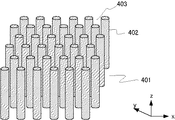
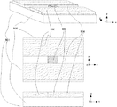
本発明で用いるフォトニック結晶の一例を図3に示す。 An example of the photonic crystal used in the present invention is shown in FIG.
図3に示したフォトニック結晶4100は構造材4101からなる2次元フォトニック結晶である。図3の例では構造材4101はZ軸方向の円柱形をなし、XY面内で規則的に配列している(以下、二次元フォトニック結晶における規則的配列が展開している面を「二次元面」と言う)。これらの柱状の構造体4101は図示していないが適当な基板上に固定され、周期が変動しないようになっている。
A
構造体の材料としては、用いる光に対して透明であればよく、シリコンやガリウムヒ素などの半導体、樹脂、SiO2等である。 The material of the structure may be transparent to the light used, and may be a semiconductor such as silicon or gallium arsenide, a resin, or SiO 2 .
空構造4102は構造材のない部分であり、この部分を標的物質を含む流体(以下「被検査流体」とも言う。「被検査液」ということもあるが、本発明のセンサが対象とするのは液体だけには限らない)が流れることになる。構造材4101中と空構造4102は2次元の周期構造をなし、その周期は2つの独立な方向で異なっていてもよい。本発明では、検出に用いる光の入射方向においてフォトニックバンドギャップが存在するフォトニック結晶を使用する。
The
周期は用いる光の波長程度もしくはそれ以下で100nm〜10μm程度の大きさである。構造材は円柱形状に限るものではなく矩形や楕円等任意の断面形状であってもよい。 The period is about 100 nm to 10 μm at or below the wavelength of the light used. The structural material is not limited to a cylindrical shape, and may have an arbitrary cross-sectional shape such as a rectangle or an ellipse.
図4はセンサ物質である結合物質がフォトニック結晶中に配置される形態を示し、図3のフォトニック結晶のXY平面内の断面図である。構造材4101の空構造4102に面した表面には検出したい物質と結合する結合物質4201が付着している。結合物質の付着密度を変えて検出感度を調節することができる。
FIG. 4 is a cross-sectional view in the XY plane of the photonic crystal of FIG. 3, showing a form in which the binding substance as the sensor substance is arranged in the photonic crystal. A binding
図5は被検査液4301を流したときの構造材4101の表面の変化を示した図である。図5(a)は被検査液に標的物質4302が含まれていなかったとき、(b)は被検査液に標的物質4302が含まれていたときの結果を示している。標的物質が含まれていなかったときは、結合物質4201は検査前と変わらないが、標的物質が含まれているとそれが結合物質4201に捕獲され、捕獲状態になる。
FIG. 5 is a view showing a change in the surface of the
標的物質一つと結合物質一つが至近距離で対峙してからの結合反応は、瞬時に起こると考えられるが、固体表面にまばらにまたは密集して担持された複数の結合物質と流体中に分散された複数の標的物質との結合反応は、全体として徐々に進行しすべての結合反応が終了するまでにはある程度の時間を要する。 The binding reaction after one target substance and one binding substance face each other at a close distance is considered to occur instantaneously, but is dispersed in a fluid with a plurality of binding substances sparsely or densely supported on the solid surface. In addition, the binding reaction with a plurality of target substances gradually proceeds as a whole, and a certain amount of time is required until all the binding reactions are completed.
本発明のセンサにおいては結合反応による周期構造の特性またはバンド構造の変化を電磁波により測定し、標的物質の存在、種類や濃度などを検出するが、測定は、結合物質を担持された周期構造に、被検査流体を流し始めてから特定の時間経過した状態で行う。特定の時間とは、周期構造に被検査流体を流し始める時を基準に、電磁波により周期構造の特性またはバンド構造の変化を測定することができるのに十分なだけ結合反応が進行する時間である。この特定の時間は、結合物質、標的物質、流体、周期構造などの種類や材料により異なる。 In the sensor of the present invention, the characteristic of the periodic structure or the change in the band structure due to the binding reaction is measured by electromagnetic waves to detect the presence, type, concentration, etc. of the target substance, but the measurement is performed on the periodic structure carrying the binding substance. In a state where a specific time has passed since the fluid to be inspected started to flow. The specific time is the time that the binding reaction proceeds sufficiently to be able to measure the characteristics of the periodic structure or the change in the band structure by the electromagnetic wave with reference to the time when the fluid to be inspected starts flowing through the periodic structure. . This specific time varies depending on the type and material of the binding substance, the target substance, the fluid, the periodic structure, and the like.
被検査液が流れている間は、空構造4102の部分には被検査液4301が満たされている。被検査液に標的物質が含まれていないと結合物質4201には何も付着しないので、構造体4101周囲の屈折率は捕獲前と変わらないが、被検査液4301に標的物質4302が含まれているときは、図5(b)のように結合物質4201の領域は捕獲状態になるので、捕獲前とは異なる屈折率になる。
While the liquid to be inspected is flowing, the portion of the
フォトニック結晶4100のフォトニックバンド構造は、この屈折率変化を反映し変調を受ける。この変調によりフォトニックバンドギャップ端がシフトし、その波長の光は透過強度や反射強度、結晶中の伝播光路などが変化する。この変化を測定することにより、被検査液に標的物質が含まれているかどうかがわかり、その量が測定される。
The photonic band structure of the
この測定は、被検査液がフォトニック結晶構造中を満たしているときに行ってもよいが、被検査液を除去した後に行うこともできる。被検査液があるときとないときとではフォトニックバンド構造が異なるが、検査後の周期構造体と標的物質が付着していない周期構造体とをともに被検査液のない条件下で測定し、比較することにより標的物質の有無が決定できる。 This measurement may be performed when the test liquid fills the photonic crystal structure, but can also be performed after the test liquid is removed. The photonic band structure is different between when the test solution is present and when there is no test solution, but both the periodic structure after the test and the periodic structure to which the target substance is not attached are measured under conditions where there is no test solution. The presence or absence of the target substance can be determined by comparison.
検査後、被検査液を他の溶液で置換した条件下で測定する場合も同様である。 The same applies when measurement is performed under the condition that the liquid to be inspected is replaced with another solution after the inspection.
また、フォトニック結晶中のすべての領域にわたり結合物質を配置し被検査液を流してもよいが、一部領域のみに結合物質を配置し、あるいは一部領域のみに被検査液を流し、当該部分に光を照射してフォトニックバンド構造の変化を測定することもできる。 Further, the binding substance may be disposed over the entire region in the photonic crystal and the test solution may be flowed. However, the binding material may be disposed only in a part of the region, or the test solution may be flowed only in the part of the region. It is also possible to measure changes in the photonic band structure by irradiating the part with light.
3.フォトニック結晶の次元
本発明は、フォトニック結晶の次元によらず適用できる。
3. Dimension of Photonic Crystal The present invention can be applied regardless of the dimension of the photonic crystal.
1次元周期構造の場合、図6のように高屈折率材料の薄膜である固体部分102が空構造である隙間103を隔てて周期的に繰り返された構造101などがある。
In the case of a one-dimensional periodic structure, there is a
また3次元の場合は、図7のように本発明の固体部分である微小球302が六方細密構造を形成するように3次元的に並んだ構造301などがあり、固体部分302の隙間303が空部分として機能する。
In the case of a three-dimensional structure, as shown in FIG. 7, there is a
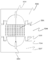
3次元のフォトニック結晶の場合、フォトニックバンド構造を設計する上で、自由度が高いというメリットがある。その反面、3次元構造であるためにどのような方向に液体を流しても凹凸があり、淀みや流れの不均一性が生じやすい。このため、被検査液被の流速に差が発生し標的物質が結合物質に均一に付着しない可能性があり、時として検出感度や結果の信頼性に影響を与える。 In the case of a three-dimensional photonic crystal, there is an advantage that the degree of freedom is high in designing a photonic band structure. On the other hand, since it has a three-dimensional structure, it has irregularities regardless of the direction in which the liquid flows, and stagnation and non-uniformity of flow are likely to occur. For this reason, a difference occurs in the flow rate of the liquid to be inspected, and the target substance may not adhere uniformly to the binding substance, sometimes affecting the detection sensitivity and the reliability of the result.
2次元フォトニック結晶を用いると、よどみや流速の場所による差異が抑えられるというメリットがある。 The use of a two-dimensional photonic crystal has the advantage that differences due to stagnation and flow velocity can be suppressed.
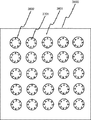
個体部分が正方格子状に配列していた図3とは別の2次元の周期構造401を図8に示す。この周期構造は、固体部分402として高さ1μm、半径 約110nmのシリコンの円柱が格子定数約390nmで、図3では正方格子状に配列していたのを、三角格子状に二次元に配列させたものであり、その隙間の部分403が空部分である。周期構造全体の大きさは、縦およそ100μm、横およそ100μmである。
FIG. 8 shows a two-dimensional periodic structure 401 different from FIG. 3 in which the individual portions are arranged in a square lattice pattern. In this periodic structure, silicon cylinders having a height of 1 μm and a radius of about 110 nm as the
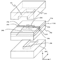
図9はさらに別の二次元の周期構造である。図9中紙面右の図は、紙面左の図のA-Bでの切断図である。固体部分202は一つながりの連続体で、これに空部分である孔203が周期的に並んだ構造201である。
FIG. 9 shows another two-dimensional periodic structure. The drawing on the right side of FIG. 9 is a cross-sectional view taken along line AB of the drawing on the left side of the drawing. The
このように構造材中に孔が形成されているフォトニック結晶を用いる場合は、標的物質と反応する結合物質3701は図10に示すように構造材3601の孔3602の側壁面に付ける。被検査液は図9の孔の中を流れることになり、この、孔の長軸方向を本明細書は「軸方向」と称する。被検査液が流れる方向には特に凹凸はないので、被検査液は孔の中をよどむことがなくスムーズに通過できる。その結果標的物質は結合物質3701に均等に付着することができる。
In the case of using a photonic crystal in which holes are formed in the structural material in this way, the binding
本発明では、標的物質と結合物質の接触が効率よく行われるように、標的物質を含む流体をフォトニック結晶の構造に応じて特定の方向に流すことが可能である。また、検出光の照射方向に適合したフォトニック結晶の配置を選ぶことにより、周期構造体から出射される電磁波の測定と屈折率の周期分布の変化の検出を並行して行うことができる。さらに流路中に複数個のセンサを置くこともできる。以上の本発明の優位点を考慮すると、本発明で用いるフォトニック結晶は2次元のフォトニック結晶が好ましい。 In the present invention, the fluid containing the target substance can be caused to flow in a specific direction according to the structure of the photonic crystal so that the target substance and the binding substance can be efficiently contacted. Further, by selecting the arrangement of the photonic crystal suitable for the irradiation direction of the detection light, the measurement of the electromagnetic wave emitted from the periodic structure and the detection of the change in the periodic distribution of the refractive index can be performed in parallel. Furthermore, a plurality of sensors can be placed in the flow path. Considering the above advantages of the present invention, the photonic crystal used in the present invention is preferably a two-dimensional photonic crystal.
4.検出方法
検出対象物質の付着によるフォトニックバンド構造の変化の検出方法としては、次の(1)ないし(3)の方法がある。
4. Detection Method The following (1) to (3) are methods for detecting a change in the photonic band structure due to the attachment of the detection target substance.
(1)フォトニックバンドギャップの変化を透過率または反射率から検出するか、もしくはバンドギャップ端前後を含む波長可変の光源を用い、透過光スペクトルを測定し、フォトニックバンドギャップ端の変化を検出する。 (1) Change in photonic bandgap is detected from transmittance or reflectance, or a variable wavelength light source including before and after the bandgap edge is used to measure the transmitted light spectrum, and change at the photonic bandgap edge is detected. To do.
(2)フォトニック結晶中に屈折率の周期が乱された欠陥構造をつくり、これによりバンドギャップ内の欠陥準位を生じさせる。この透過光強度の変化を観測する。 (2) A defect structure in which the refractive index period is disturbed is formed in the photonic crystal, thereby generating a defect level in the band gap. This change in transmitted light intensity is observed.
(3)フォトニックバンド構造の変化による、フォトニック結晶構造中を透過する光の経路の変化を検出する。 (3) A change in the path of light transmitted through the photonic crystal structure due to a change in the photonic band structure is detected.
以下、詳しく説明する。 This will be described in detail below.
(検出方法1)
図11において3401はフォトニック結晶、3402はこのフォトニック結晶に光を照射するレーザなどの光照射手段である。フォトニック結晶は、図3に示す柱状の構造材が規則配列したものを用いる。なお、フォトニック結晶の2次元面を図中の白い丸のマトリクスで模式的に表している。図15、18、20及び21においても同様である。柱の間隙に被検査液を流し、標的物質を付着させる。透過光3403が信号光検出器3404に入り検出される。透過光を検出する代わりに反射光を検出してもよい。
(Detection method 1)
In FIG. 11, 3401 is a photonic crystal and 3402 is a light irradiation means such as a laser for irradiating the photonic crystal with light. As the photonic crystal, a regular arrangement of columnar structural materials shown in FIG. 3 is used. The two-dimensional surface of the photonic crystal is schematically represented by a white circle matrix in the figure. The same applies to FIGS. 15, 18, 20 and 21. The test liquid is allowed to flow through the gaps between the pillars to adhere the target substance. The transmitted light 3403 enters the
光源3402はフォトニックバンドギャップの端近くの波長の光を出射し、検出器3404は、同じ波長の光の強度変化を検出する。
The
フォトニックバンドギャップの長波長端の、ギャップの内側の光を照射し、透過光を観測すると、バンドギャップが短波長側にシフトしたとき、測定光波長がバンドギャップの外にくるので、透過光強度の増加として観測できる。試料に照射する光は、バンド端の波長近傍の光を選ぶが、その近傍とは、標的物質の付着によってバンド端がシフトする範囲であることは言うまでもない。 When irradiating light inside the gap at the long wavelength end of the photonic band gap and observing the transmitted light, when the band gap shifts to the short wavelength side, the measured light wavelength is outside the band gap, so the transmitted light It can be observed as an increase in intensity. As the light to be irradiated on the sample, light in the vicinity of the wavelength at the band edge is selected. Needless to say, the vicinity is a range in which the band edge shifts due to adhesion of the target substance.
あるいは、波長可変レーザを光源3402として用い、バンドギャップの長波長端または短波長端いずれかのバンド端を含む範囲で波長をスキャンして透過率スペクトルを測定し、その変化を見てもよい。
Alternatively, a wavelength tunable laser may be used as the
(検出方法2)
フォトニック結晶に結晶欠陥を導入することにより、バンドギャップ内に欠陥準位が生じ、その準位の波長の光が透過するようになる。この透過光の変化を測定することにより標的物質を検出する。
(Detection method 2)
By introducing a crystal defect into the photonic crystal, a defect level is generated in the band gap, and light having a wavelength of that level is transmitted. The target substance is detected by measuring the change in the transmitted light.
図12は欠陥が導入された柱状構造のフォトニック結晶を示す。欠陥部の柱状構造体3801は周囲の柱状構造体4101に比べて太くなっている。
FIG. 12 shows a photonic crystal having a columnar structure in which defects are introduced. The
欠陥の構造としては、図13に示すように周囲の柱状構造に比べて半径が小さい柱状構造3901を入れるような構造や、図14に示すように柱状構造の欠損4001等、周期構造を乱すものであれば何でもよい。ただし、本発明による検出を行うためにはこの結晶欠陥により生じる準位がフォトニックバンドギャップ中にある必要がある。
As the defect structure, a structure in which a
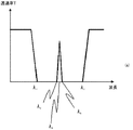
欠陥構造を含んでいるフォトニック結晶3501に、図15に示すように欠陥3502部位を狙って光3503を導入する。図において3504は透過光、3505は反射光を示している。
As shown in FIG. 15, light 3503 is introduced into the
透過光スペクトルを図16に模式的に示す。図16のスペクトルにおいて横軸は波長、縦軸は透過率を示している。λ1からλ2までの間がフォトニックバンドギャップで、その中に欠陥に起因する共鳴準位λ0が発生し、λ0近傍のλaからλbまでの波長の光が透過する。 The transmitted light spectrum is schematically shown in FIG. In the spectrum of FIG. 16, the horizontal axis indicates the wavelength, and the vertical axis indicates the transmittance. Between λ 1 and λ 2 is a photonic band gap, in which a resonance level λ 0 caused by a defect is generated, and light having a wavelength from λ a to λ b in the vicinity of λ 0 is transmitted.
このバンドギャップ内の透過波長帯の幅と高さは、光路に沿ったフォトニック結晶の厚さに依存する。厚さが短ければ透過率は1に近くなるが、共鳴は弱くなりλaからλbの幅が広くなる。 The width and height of the transmission wavelength band within this band gap depend on the thickness of the photonic crystal along the optical path. The thickness is shorter if the transmittance is close to 1, the resonance width of the weakened [lambda] a lambda b becomes wider.
図16に示したスペクトルは光を欠陥を通過する様にあてたときのスペクトルであって、欠陥以外の場所では透過帯は現れない。すなわち、入射する光ビームに広がりがあるとこの透過帯の透過率が下がり、その変化も観測困難である。したがって、照射する光は、十分コリメートされ、かつ狭く絞られたビームである必要がある。 The spectrum shown in FIG. 16 is a spectrum when light is applied so as to pass through the defect, and no transmission band appears in a place other than the defect. That is, if the incident light beam has a spread, the transmittance of this transmission band decreases, and the change is difficult to observe. Therefore, the irradiated light needs to be a sufficiently collimated and narrowly focused beam.
図17は結合物質とフォトニック結晶の形態を示す図で、図13のXY平面内のフォトニック結晶の断面図である。構造材4101の表面には欠陥部3801を含めて検出したい標的物質と結合する結合物質4201が付着している。
FIG. 17 is a view showing the form of the binding substance and the photonic crystal, and is a cross-sectional view of the photonic crystal in the XY plane of FIG. A binding
標的物質が捕獲されると、捕獲された物質の存在する場所の屈折率は捕獲前と異なっていることになる。このような変化は欠陥部3801でも発生する。これがフォトニック結晶のフォトニックバンド構造を変調することになり、さらに欠陥準位のエネルギーも変化する。すなわち、図16において示した各波長がシフトすることになる。本発明によるセンサではこの欠陥エネルギーのシフトによる光の透過率または反射率の変化を検出することにより標的物資を検出する。
When the target substance is captured, the refractive index of the place where the captured substance exists is different from that before the capture. Such a change also occurs in the
本発明による標的物質の検出方法を図18に示す。フォトニック結晶構造4401は例えばこれまでに説明してきたような欠陥3801を含むフォトニック結晶構造で、図17に示すように結合物質4201を含んでいる。このフォトニック結晶の欠陥部を狙って光源4402から光が導入される。フォトニック結晶構造4401の中に存在する空構造には検査対照となる被検査液が導入され、被検査液の中に標的物質があると結合物質に捕獲され透過スペクトル及び反射スペクトルが変化する。本発明ではとくに欠陥部分に起因した共鳴による透過光、反射光の変化を検出する。
FIG. 18 shows a method for detecting a target substance according to the present invention. The
結合物質による標的物質の捕獲の有無による透過スペクトルの変化を図19に示す。図19は欠陥に起因する共鳴付近の波長のスペクトルを示しており、図19(a)は捕獲がないとき、(b)は捕獲があるときのスペクトルであり捕獲の有無により共鳴ピークの位置がずれる。(a)において、λ0が共鳴の中心周波数であり、これにともなう透過の領域がおよそλaからλbまでの範囲に広がっている。標的物質に捕獲により、それぞれがダッシュ(')のついた長波長側にシフトしている(図19(b))。図19におけるこの差異を検出することにより被検査液中標的物質の有無を検出することが可能となる。この共鳴による透過ピークは鋭いため、わずかなピーク位置の変化が検出でき、結合物質の捕獲の有無を感度よく検出することができる。 FIG. 19 shows changes in the transmission spectrum depending on whether or not the target substance is captured by the binding substance. Fig. 19 shows the spectrum of the wavelength near the resonance caused by the defect, Fig. 19 (a) is the spectrum when there is no capture, (b) is the spectrum when there is capture, and the position of the resonance peak depends on the presence or absence of capture. Shift. In (a), λ 0 is the center frequency of resonance, and the transmission region associated therewith extends over a range from λ a to λ b . Each is shifted to the long wavelength side with a dash (') due to capture by the target substance (FIG. 19 (b)). By detecting this difference in FIG. 19, it is possible to detect the presence or absence of the target substance in the test liquid. Since the transmission peak due to this resonance is sharp, a slight change in peak position can be detected, and the presence or absence of capture of the binding substance can be detected with high sensitivity.
検出の方法はフォトニック結晶4401を透過してきた透過光4403または反射光4405を検出することにより行う。光源4402として共鳴波長λ0前後を含む光源を用い、透過光または反射光のスペクトルを検出し、共鳴波長の変化を検出するというのが一つの方法である。
The detection method is performed by detecting transmitted light 4403 or reflected light 4405 transmitted through the
また、λaからλbの間の一つの波長の光に注目し、その光の強度変化を検出する方法でもよい。例えば、λaとλ0の間のある波長の透過光を観察する場合、ピーク波長λ0が高波長側にシフトした場合、これを透過光強度の減少として観測できる。 Alternatively, a method of paying attention to light of one wavelength between λ a and λ b and detecting the intensity change of the light may be used. For example, when observing transmitted light having a certain wavelength between λ a and λ 0 , if the peak wavelength λ 0 is shifted to the higher wavelength side, this can be observed as a decrease in transmitted light intensity.
(検出方法3)
標的物質の検出すなわち結合物質への付着にともなうフォトニックバンド構造の変化を、フォトニック結晶構造中を透過する光の経路の変化あるいは光の進行方向の変化で検出することもできる。
(Detection method 3)
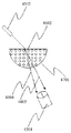
The change in the photonic band structure accompanying the detection of the target substance, that is, the attachment to the binding substance, can also be detected by a change in the path of light passing through the photonic crystal structure or a change in the traveling direction of the light.
図20にその方法を示す。フォトニック結晶構造4501は図3で説明したような結合物質を含んだフォトニック結晶であり、紙面がXY平面に対応する。入射面4602を通して光源4502から光が導入される。この光は感度を上げるためにはなるべく単色で、コリメートした光が望ましく、そのためには光源4502としてはレーザ光が望ましい。また途中には光をコリメートする光学系を入れることが望ましい。フォトニック結晶構造4501の中に存在する空構造には検査対照となる被検査液が導入され、被検査液の中に標的物質である抗原または抗体があると結合物質に捕獲されフォトニックバンド構造が変化する。この変化にともない、フォトニック結晶構造中を進行する光の光路が変化する。フォトニック結晶4501から出射面4606を通して出てきた光の進行方向は、標的物質の有無にかかわりなく同じであるが、その位置は、フォトニック結晶中の光の進行方向により変化する。図20には標的物質の付着していない場合と付着した場合の光路を4604と4605で示している。光路の先には検出器4504があり、光路の変化を検出する。この検出器としては例えばフォトダイオードを2つ並べて検出器として使う2分割センサ等が挙げられる。検出器からの出力をあらかじめ決められた算出法により計算すれば、標的物質の量を正確に求めることができる。
FIG. 20 shows the method. The
図20ではフォトニック結晶への光の入射面と出射面が平行面になっているが図21に示すようにフォトニック結晶中での光路の変化を検出しやすくするために、出射面を入射位置を中心に円形を形成してもよい(4701で示した面)。このような形状にしておくことで、フォトニック結晶を出るとき、その出射面4701で屈折が発生せず、フォトニック結晶中での光の進行方向がフォトニック結晶外でも保存され、このフォトニック結晶外での検出位置を遠ざけることにより感度を上げることができる。
In FIG. 20, the light incident surface and the light exit surface are parallel to the photonic crystal. However, as shown in FIG. 21, the light exit surface is incident to make it easier to detect changes in the optical path in the photonic crystal. A circle may be formed around the position (surface indicated by 4701). With this shape, when exiting the photonic crystal, no refraction occurs on the
フォトニック結晶に光を入射させたとき、わずかな入射角の違いでフォトニック結晶構造中の光の進行方向が大きく変化する現象がスーパープリズム効果として知られている(日本物理学会誌第55巻(2000年)、3月号、172-179ページ)。入射角が同じで入射光の波長がわずかに違ってもフォトニック結晶構造中の光の進行方向が大きく変化する。 It is known as a super prism effect that light travels in a photonic crystal structure with a slight difference in incident angle when light is incident on the photonic crystal (Volume 55 of the Physical Society of Japan). (2000), March issue, pages 172-179). Even if the incident angle is the same and the wavelength of the incident light is slightly different, the traveling direction of the light in the photonic crystal structure changes greatly.
このようなスーパープリズム効果はフォトニック結晶への光の入射方向と波長が特定の領域で発生する(日本物理学会誌第55巻(2000年)、3月号、172-179ページ)。 Such a super prism effect occurs in a specific region in which the incident direction and wavelength of light to the photonic crystal are (The Physical Society of Japan Vol. 55 (2000), March issue, pages 172-179).
図22を用いて簡単に説明する。 This will be briefly described with reference to FIG.
図22は波数空間の図である。4801はフォトニック結晶と外部との境界面の方向にあたる。図において入射光の波数ベクトルは4802で示している。4803はフォトニック結晶中で入射エネルギーと同じエネルギーを持つ等エネルギー面、4804は入射光の波数ベクトル4802の入射面に平行な成分である。
FIG. 22 is a diagram of the wave number space. 4801 corresponds to the direction of the interface between the photonic crystal and the outside. In the figure, the wave number vector of the incident light is indicated by 4802. 4803 is an isoenergy surface having the same energy as the incident energy in the photonic crystal, and 4804 is a component parallel to the incident surface of the
フォトニック結晶での光のエネルギーの進行方向は4803と4804の交点4805でのエネルギー分散面の傾き方向となる。図では4805におけるエネルギー分散面の傾き方向、すなわちフォトニック結晶中での光のエネルギーの進行方向を4806で示している。
The traveling direction of light energy in the photonic crystal is the tilt direction of the energy dispersion plane at the
この場合入射光の波数ベクトル4802が少し変化してもフォトニック結晶中の光の進行方向4806は大きくは変化しない。図22において入射角がわずかに変化した場合の波数ベクトルを4807で示す。この場合フォトニック結晶への入射光の波数ベクトル4807の境界面方向4801に平行な成分は4808であり、交点4805に対応する点は交点4809となる。この点でのエネルギー分散面の傾きが光の進行方向になるので、光のエネルギーはフォトニック結晶中では図示4810の方向に進行することになり4808と向きは大きくは変わらない。すなわち入射光の波長や方向が変化してもフォトニック結晶構造中の光のエネルギーの進行方向は大きくは変化しない。
In this case, even if the
ところが図23に示すように同じフォトニック結晶に対して入射光の波数ベクトル4901をとると(エネルギーは図22の場合と同じで入射方向が異なる)、図22中の交点4805に対応する点は図23では図示4902となり光のエネルギーの進行方向は図示4903の方向となる。この場合、入射光の波数ベクトル4901がわずかに変化して4904になると、交点は4905になり、光のエネルギーの進行方向は4906になる。このように入射光の波数ベクトルがわずかに変化しただけフォトニック結晶中の光の進行方向が大きく変化する。
However, as shown in FIG. 23, when the
このような光のエネルギーの進行方向の大きな変化はフォトニック結晶構造中のフォトニックバンド構造がわずかに変化した場合にも発生する。すなわちフォトニック結晶構造がわずかに変化するとエネルギー分散面が変化し、交点4902の位置が変化するとともに、エネルギーの進行方向が大きく変化する。この効果をスーパープリズム効果といい、この効果が発生するためには交点4805、4902における等エネルギー面が大きな曲率をもっていればよいことになる。
Such a large change in the traveling direction of light energy occurs even when the photonic band structure in the photonic crystal structure is slightly changed. That is, when the photonic crystal structure slightly changes, the energy dispersion plane changes, the position of the
このように入射光の波数ベクトルを選べばわずかなフォトニック結晶構造の変化で光の進行方向を大きく変えるとことができる。すなわちこの入射方向を用いれば、フォトニック結晶構造中に付着した標的物質を大きな感度で検出することができる。 Thus, if the wave number vector of incident light is selected, the traveling direction of light can be greatly changed by a slight change in the photonic crystal structure. That is, if this incident direction is used, the target substance attached in the photonic crystal structure can be detected with high sensitivity.
5.フォトニック結晶の配置
次に流路中のフォトニック結晶の配置について説明する。
5. Arrangement of Photonic Crystal Next, the arrangement of the photonic crystal in the flow path will be described.
A.流路と交差した光を照射する配置
A-1.周期構造が流路に平行である場合
図24は、本発明における周期構造体すなわちフォトニック結晶を、被検査液などの流体を流す流路の一部に設けてセンサとした、センサチップの模式図である。
A. Arrangement for irradiating light that intersects the flow path A-1. When the periodic structure is parallel to the flow path FIG. 24 shows a flow of fluid such as a liquid to be inspected through the periodic structure in the present invention, that is, a photonic crystal. It is a schematic diagram of a sensor chip provided as a sensor in a part of a flow path.
本センサチップは流路504と図3に示すような空構造が連続しその中に円柱構造がある二次元フォトニック結晶503を含み構成される。このセンサチップの流路の両端は流体を抽出して流路へ導入したり、流体を成分ごとに分離したりするような構造に結合されているが、そのような全体の構成のうち本例はじめ本明細書中の実施形態および実施例においては、特に標的物質の検出につかさどる部分を図示して説明する。
The sensor chip includes a
センサチップ501は、SOI(Silicon on Insulator)基板の厚さ1μmの絶縁層505上の厚さ500nmのSOI層を半導体プロセス技術により加工して作製する。フォトリソグラフィーにより流路の壁となる流路壁502を、EB(電子線)描画、現像、ドライエッチング技術により、流路の一部に設けられた周期構造であるフォトニック結晶503を同様にSOI層に作製する。このフォトニック結晶503は、図3に示す円柱を配列したフォトニック結晶401の空構造側の表面に結合物質として抗体を担持したものである。
The
また、二つの流路壁502に挟まれた領域は流路504として機能する。図24のy方向が流路の方向すなわち被検査液などの流体を流す方向である。図24において流路504上方つまりz方向には、物質が存在しないように図示されているが、実際は流路から流体が漏れないように、SOI層の上にガラスや、樹脂などにより流路上方に蓋をした構成とする。図24は、説明の便宜上この蓋を省略して描いてある。また、以下の例においても、この蓋は省略されて描かれているものとする。
A region sandwiched between the two
流路504の両端は、別の流路や、流体を抽出したり流体を成分ごとに分離したりするなどの工程を担う別の構造体へと結合されている。
Both ends of the
流路504中を水の中に抗原が分散された流体が流れ、この流体がフォトニック結晶503を通過する際に、流体中の抗原とフォトニック結晶の空構造403側に担持された抗体が抗原抗体反応つまり結合反応を起こして、流体中の抗原はフォトニック結晶503に固定化されている抗体に特異的に結合し、固定化される。このことによりフォトニック結晶のフォトニックバンド構造が変化し、TE偏光の波長に対する透過率特性が変化する。例えば図2中のバンド端3001が短波長側にシフトすることになる。抗原抗体反応前後での透過光強度を比較すれば標的物質、この例では抗原を、検出することができる。
The fluid in which the antigen is dispersed in water flows through the
図25は測定用の光を上述のセンサチップに照射し且つ特性の変化を検出する光学系を配置した、本発明の装置の全体構成例である。センサチップの2次元フォトニック結晶503は、周期構造が図3に示されるような固体の構造材から成り、その長軸方向が流路の底面に垂直なものである。2次元面に平行な平面をXY平面としているのでセンサチップ面はXY面に平行である。被検査液の流れ方向をX軸方向とする。電磁波発生源であるレーザ602と光学系603よりなる電磁波照射手段601からの波長1550nmのレーザ光605が放射され、偏波制御手段である偏光板604によってTEモードが選ばれる。そのフォトニックバンド端の波長のTE偏光は、フォトニック結晶503側面で集光するように集光レンズ609で絞って、センサチップ501の流路壁502の側面に照射され、フォトニック結晶503に入射する。したがって、光の入射方向はY軸方向である。すなわち本実施形態におけるフォトニック結晶の2次元面(XY平面)は光の入射方向(Y軸)に平行で且つ流れの方向(X軸)に平行である。
フォトニック結晶を透過した光はもう一方の流路壁502の側面から出射される、この光(信号光)606をレンズ610でコリメートして偏光制御手段である偏光板607を通ることで、TM偏光成分だけを取り出して、最終的にレンズ611により集光して電磁波検出器であるフォトダイオード608で検出する。
FIG. 25 shows an example of the overall configuration of the apparatus of the present invention in which an optical system for irradiating the above-described sensor chip with light and detecting a change in characteristics is arranged. The two-
The light transmitted through the photonic crystal is emitted from the side surface of the other
抗原抗体反応前後では、フォトニック結晶503のバンド端に相当する1550nmの光の透過率は変化するので、それぞれを測定して差をとれば標的物質である抗原を検出できることになる。また、抗原が抗体に結合して固定化された後、一度流路およびフォトニック結晶を水などで洗い流してから、透過光強度を測定してもよいし、洗い流さないで測定してもよい。流体中の抗原の濃度により、流体を流し始めてから一定の時間における透過光強度の変化は異なるので、例えば、時間で規格化して透過光強度の変化を測定することにより、流体中の抗原の濃度なども測定することができる。
Before and after the antigen-antibody reaction, the transmittance of light of 1550 nm corresponding to the band edge of the
この構成は、2次元のフォトニック結晶の周期構造が図3に示されるような固体の構造材からなるので、間隔が大きくかつ2次元周期構造のある面が流路つまり検査液被検査液の流れに対して平行な面内にあるので、被検査液はよどみなく流れる。したがって流路断面積を小さく設定でき、さらに検出のための光はフォトニック結晶の周期構造面に平行かつ流路に対して直行する方向に照射することができるので、光源から検出器までの距離を短くでき、装置全体がコンパクトになる。 In this configuration, since the periodic structure of the two-dimensional photonic crystal is made of a solid structural material as shown in FIG. Since it is in a plane parallel to the flow, the liquid to be inspected flows smoothly. Therefore, the cross-sectional area of the channel can be set small, and the light for detection can be irradiated in a direction parallel to the periodic structure surface of the photonic crystal and perpendicular to the channel, so the distance from the light source to the detector The overall apparatus becomes compact.
また、本実施態様は標的物質と結合物質の特異的な反応を用いることから、流体中に複数の物質が分散している場合にも、目的とする特定の種類の標的物質だけを検出することが可能である。 In addition, since this embodiment uses a specific reaction between a target substance and a binding substance, even when a plurality of substances are dispersed in a fluid, only a specific target type of target substance is detected. Is possible.
A-2.周期構造が流路に直角である場合。 A-2. When the periodic structure is perpendicular to the flow path.
本発明のセンサの別の実施形態を図26を用いて説明する。センサチップ701はモールド法により作製されたアクリル樹脂よりなり、下層部(絶縁層)702の上に流路側壁壁部703に挟まれた流路704の一部にフォトニック結晶503が配置されている。
Another embodiment of the sensor of the present invention will be described with reference to FIG. The
周期構造であるフォトニック結晶503は、図9に示したように固体部分202に空構造である細孔203が周期的に並んだ構造のフォトニック結晶で、細孔の長軸方向が流路に平行に配置され、被検査液が細孔内を流れるようになっている。周期構造の2次元面は図26のyz面内にある。被検査液の流れは細孔長軸すなわちX軸に平行である。すなわち本実施形態におけるフォトニック結晶の2次元面(YZ平面)は光の入射方向(Z軸)に平行且つ流れの方向(X軸)に直交している。
A
光源を含む測定光学系601ないし611は、センサチップ701の上下に配置され、光は基板702に垂直な方向からフォトニック結晶201に照射される。偏光板604はフォトニック結晶201に入射する光がTEモードになるように配置される。
Measurement
フォトニック結晶503は、TE偏光の光に対して、フォトニックバンド構造の中の第一バンドと第二バンドの間にフォトニックバンドギャップを有し、その第一バンド端の光の波長が、1550nm付近に相当するように設計されている。抗原抗体反応により、フォトニックバンド構造が変化するに際し、フォトニック結晶中をある方向に伝播する光の波長に対する透過率特性も変化する。例えば図2中のバンド端2001が短波長側にシフトすることになる。透過率特性のグラフを考えたときに、バンド端領域のある波長の光をフォトニック結晶に入射して、抗原抗体反応前後での透過光強度を比較すれば抗原を検出することができる。
The
被検査液を流路からフォトニック結晶に通すことにより、抗原抗体反応を起こす。レーザ601と光学系603よりなる電磁波照射手段601からの波長1550nmの光605を偏光制御手段である偏光板604を通し、フォトニック結晶503表面で集光されるようにレンズ609で絞って、照射する。フォトニック結晶503を透過した光606をレンズ610でコリメートして偏光板607を通して、レンズ611で集光しフォトダイオード608で検出する。A-1の実施形態と同様に、抗原抗体反応前後での透過光強度の変化を測定することにより、抗原を検出するものである。
An antigen-antibody reaction is caused by passing the liquid to be inspected from the flow path through the photonic crystal.
この構成は、2次元のフォトニック結晶が、図9に示すような細孔構造であり、被検査液がよどみなく流れるためには、細孔の長さつまりフォトニック結晶の厚さは被検査液の粘度に応じて薄く形成する必要がある。反面、周期構造の二次元面(XY面)が流路つまり被検査液の流れに対して垂直なので、検出のための光はフォトニック結晶の2次元周期構造面(yz面)に平行かつセンサチップ基板702に対して垂直な方向から照射することができる。その結果、A-1の例よりもさらに光源から検出器までの距離を短くでき、装置全体が一層コンパクトになる。
In this configuration, the two-dimensional photonic crystal has a pore structure as shown in FIG. 9, and the length of the pore, that is, the thickness of the photonic crystal, is to be inspected in order for the inspection liquid to flow without stagnation. It is necessary to form thinly according to the viscosity of the liquid. On the other hand, since the two-dimensional surface (XY surface) of the periodic structure is perpendicular to the flow path, that is, the flow of the liquid to be inspected, the light for detection is parallel to the two-dimensional periodic surface (yz surface) of the photonic crystal and the sensor Irradiation can be performed from a direction perpendicular to the
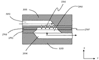
A-3.反射光を測定する場合
図27は、フォトニック結晶からの反射光の強度変化を測定する方法を用いた例である。フォトダイオード608他の光検出系が光源系と同じく基板の上方に配置されている。また、レーザ光をフォトニック結晶の所定位置に照射し、所定位置からの反射光を検出するためのアライメント手段801、802、センサチップの温度を制御するための、温度コントローラ804、及び温度コントローラ804に接続された温度制御手段803を配置している。他は、A-2と同じ構成である。
A-3. Case of Measuring Reflected Light FIG. 27 shows an example using a method of measuring the intensity change of reflected light from a photonic crystal. Similar to the light source system, the
入射光と反射光はYZ面内にあり、フォトニック結晶に対して所定角度で入射し反射する。レーザ光源603の波長と偏光板604の偏光方向は、フォトニック結晶503のバンド端に相当する光がTEモードで照射されるように設定される。フォトニック結晶503は図9に示す孔構造体で孔の長軸が流路に平行に、すなわちX方向に置かれている。これに対してTEモードの光605は、図のX方向に電場成分をもつ偏光した光である。
Incident light and reflected light are in the YZ plane, and are incident on the photonic crystal at a predetermined angle and reflected. The wavelength of the
フォトニック結晶503は、また図8に示した円柱構造体であってもよい。このとき、フォトニック結晶503は円柱が図27のZ方向に平行になるように配置され、入射光605がYZ面内に電場成分を持つ偏光状態となるよう、偏光板604が設定される。
The
A-1、A-2またはA-3の構成で、フォトニック結晶を図6に示す1次元構造に置き換えることもできる。被検査液がよどみなく流れるように、流路は図6の薄膜構造の薄膜102に平行に取り、光は薄膜102に垂直にまたは所定角度で入射する。
In the configuration of A-1, A-2, or A-3, the photonic crystal can be replaced with a one-dimensional structure shown in FIG. The flow path is taken in parallel to the
あるいは図7に示す3次元のフォトニック結晶に置き換えてもよい。3次元フォトニック結晶を球形の構造体を積み重ねて構成すると、その隙間を被検査液が流れるので、流路に対して任意の方向にフォトニック結晶を配置することができる。 Alternatively, it may be replaced with a three-dimensional photonic crystal shown in FIG. When the three-dimensional photonic crystal is formed by stacking spherical structures, the liquid to be inspected flows through the gap, so that the photonic crystal can be arranged in an arbitrary direction with respect to the flow path.
B.流路に平行に光を照射するとき
光を流路内に導き、流路に沿って進行させ、流路途中にあるフォトニック結晶に入射させることもできる。後の例で詳しく説明するが、図33に示すように、流路をフォトニック結晶の上流と下流の両側で90°折り曲げ、折り曲げ部分から外部光を流路内に導き、フォトニック結晶を透過させ、もう一方の折り曲げ部分から外部に取りだす。
B. When irradiating light parallel to the flow path, the light can be guided into the flow path, traveled along the flow path, and incident on the photonic crystal in the middle of the flow path. As will be described in detail later, as shown in Fig. 33, the flow path is bent 90 ° on both the upstream and downstream sides of the photonic crystal, and external light is guided into the flow path from the bent portion and transmitted through the photonic crystal. And take it out from the other bent part.
この構成は、流路の長手方向に光路があるので、光路を短くすることが困難であるが、次に説明するように、複数のフォトニック結晶を流れに沿って上流、中流、下流に配置し、これらを貫くように光を透過させることにより、単一の光源で複数のセンサの測定ができるというメリットがある。 In this configuration, since there is an optical path in the longitudinal direction of the flow path, it is difficult to shorten the optical path. However, as will be described below, a plurality of photonic crystals are arranged upstream, midstream, and downstream along the flow. However, by transmitting light so as to penetrate these, there is an advantage that a plurality of sensors can be measured with a single light source.
6.複数センサ構成
被検査液中に複数の標的物質が含まれているとき、各々に標的物質と固有に反応する結合物質を付着させた複数のフォトニック結晶を流路中に配置し、それぞれを測定することによって、複数の標的物質を同時に検出することができる。
6. Multiple sensor configuration When multiple target substances are included in the solution to be inspected, multiple photonic crystals each having a binding substance that reacts specifically with the target substance are placed in the flow path. By measuring, a plurality of target substances can be detected simultaneously.
複数のフォトニック結晶の配置の仕方によって異なる構成のセンサが考えられる。以下それらについて説明する。 Sensors having different configurations are conceivable depending on the arrangement of a plurality of photonic crystals. These will be described below.
C.流路に対し直列にフォトニック結晶を配置した構成
C-1.複数光源で測定する場合
図28、29に、A-1で説明した図25、26のフォトニック結晶を、流路中に複数個直列配置したセンサの例を示す。ここでいう直列とは、流路に沿って上流から下流に並んで配置された状態をいう。配置は流路方向に厳密に一直線上である必要はなく、構造および測定光学系の配置に応じて適宜選択されてよい。
C. Configuration in which photonic crystals are arranged in series with the flow path C-1. When measuring with multiple light sources FIGS. 28 and 29 show the photonic crystals of FIGS. 25 and 26 described in A-1 in the flow path. Shows an example of sensors arranged in series. Here, the term “series” refers to a state in which they are arranged along the flow path from upstream to downstream. The arrangement does not have to be strictly in line with the flow path direction, and may be appropriately selected according to the structure and arrangement of the measurement optical system.
図28は一つの流路に3つのフォトニック結晶を配置した構成のセンサチップ901を示す図である。
FIG. 28 is a diagram showing a
SOI基板の厚さ2μmの絶縁層902上にフォトリソグラフィーにより障壁部903に挟まれた領域に流路904、幅5μmの光導波路908と909、フォトニック結晶907が位置する領域を作製し、フォトニック結晶の構造はEBリソグラフィーを用いて作製する。
A region where the
フォトニック結晶905、906、907は、図9に示すものと同様にシリコンの円柱が三角格子状に二次元に配列したものである。フォトニック結晶905、906、907のサイズは、縦100μm、横100μm、高さ1μmであり、流路904は幅100μm、高さ1μmである。
The
フォトニック結晶905、906、907は、それぞれ別々の抗体が担持され、その状態で異なる波長領域のバンドギャップを有し、検出に用いるバンド端の波長もそれぞれ異なるように設計されている。
The
三つのフォトニック結晶は、異なる三種類の抗体をその空構造側の表面に担持されていて、フォトニック結晶ごとに検出する抗原の種類は異なる。つまりこのセンサチップ一つで、異なる三種類の抗原を検出することが可能である。また、光導波路に光を閉じ込めるために、光導波路908、909と障壁部903との間には、2μmの距離を設けてある。
The three photonic crystals carry three different types of antibodies on the surface of the empty structure side, and the type of antigen to be detected is different for each photonic crystal. That is, it is possible to detect three different types of antigens with this single sensor chip. In order to confine light in the optical waveguide, a distance of 2 μm is provided between the
このセンサチップを用いて、複数種類の標的物質を検出する構成を図29に示す。三つのフォトニック結晶に対して、光による検出系も三構成用意する。 A configuration for detecting a plurality of types of target substances using this sensor chip is shown in FIG. For three photonic crystals, three light detection systems are also prepared.
半導体レーザ1004と光学系1007のなす電磁波照射手段1001、偏波制御手段としての偏光板1010、レンズ1013、レンズ1022、偏波制御手段としての偏光板1025、アライメント手段1028およびフォトダイオード1031が、光による第一の検出系をなす。
An electromagnetic wave irradiation means 1001 formed by a
半導体レーザ1005と光学系1008のなす電磁波照射手段1002、偏波制御手段としての偏光板1011、レンズ1014、レンズ1023、偏波制御手段としての偏光板1026、アライメント手段1029およびフォトダイオード1032が、光による第ニの検出系をなす。
An electromagnetic wave irradiation means 1002 formed by a
半導体レーザ1006と光学系1009のなす電磁波照射手段1003、偏波制御手段としての偏光板1012、レンズ1015、レンズ1024、偏波制御手段としての偏光板1027、アライメント手段1030およびフォトダイオード1033が、光による第三の検出系をなす。
An electromagnetic wave irradiation means 1003 formed by a
第一、第二、第三の検出系はそれぞれフォトニック結晶905、906、907に対応している。偏光板1010、1011、1012は光をセンサチップ面に対してTM偏光に制御するものである。
The first, second, and third detection systems correspond to the
半導体レーザ1004、1005、1006はそれぞれ、三種類の抗体が別々に担持されたフォトニック結晶905、906、907のフォトニックバンド構造におけるフォトニックバンドギャップのバンド端領域中心付近の波長を発生させるものである。よって半導体レーザ1004、1005、1006は異なる波長の光を発生させるものである。
電磁波発生手段1001、1002、1003からの3つのレーザ光1016、1017、1018は偏光板、レンズを通って、センサチップの一方の三本の光導波路908に結合され導波路中を伝播してフォトニック結晶905、906、907に達する。3つのフォトニック結晶からの三本の光はもう一方の三本の導波路909を通って、信号光1019、1020、1021としてセンサチップ外に出射され最終的には、それぞれに対応したフォトダイオード1031、1032、1033により測定される。
The three
本構成は、フォトニック結晶ごとに光源と光学系が必要であるが、フォトニック結晶905-907を共通化できるというメリットがある。また、それぞれ光路が独立なので、バンドギャップはお互いに無関係に任意に選ぶことができ、任意の結合物質について検出できることも利点である。また、フォトニック結晶もすべて図9の構造でなくてよく、一部または全部をA-2、A-3で説明した構成で置き換えてもよいことは言うまでもない。 This configuration requires a light source and an optical system for each photonic crystal, but has an advantage that the photonic crystals 905-907 can be shared. Further, since the optical paths are independent from each other, the band gap can be arbitrarily selected irrespective of each other, and it is also advantageous that any binding substance can be detected. Further, it is needless to say that all the photonic crystals may not have the structure shown in FIG. 9, and a part or all of them may be replaced with the configuration described in A-2 and A-3.
抗原の分散された流体を流路からフォトニック結晶に流す前と後では、抗原抗体反応により、フォトニック結晶の特性が変化するので、バンド端における透過率が変化する。つまり、抗原抗体反応前後でのそれぞれのフォトニック結晶905、906、907のバンド端領域内の波長の光の透過強度を測定、比較することにより、流体中の三種類の抗原を同時に検出することができる。抗体の種類を変えることにより、検出する標的物質である抗原の種類も選択することができる。
Before and after flowing the fluid in which the antigen is dispersed from the flow path to the photonic crystal, the characteristics of the photonic crystal change due to the antigen-antibody reaction, so that the transmittance at the band edge changes. In other words, three types of antigens in a fluid can be detected simultaneously by measuring and comparing the transmission intensity of light within the band edge region of each
また、本実施形態において、三つのフォトニック結晶に担持された三種類の抗体に特異的に結合する三種類の抗原以外の物質が、流体中に存在しているとしてもそれらは、フォトニック結晶に担持された抗体と特異的に結合するものではないので、目的とした三種類の抗原を選択的に検出することができる。 Further, in the present embodiment, even if substances other than the three types of antigens that specifically bind to the three types of antibodies carried on the three photonic crystals are present in the fluid, they are not included in the photonic crystal. Since it does not specifically bind to the antibody carried on the carrier, it is possible to selectively detect the intended three types of antigens.
C-2.単一光源で測定する場合
図30は、一つの電磁波発生手段で、複数の標的物質を検出するための本発明におけるセンサの1例を示す図である。
C-2. When Measuring with a Single Light Source FIG. 30 is a diagram showing an example of a sensor in the present invention for detecting a plurality of target substances with one electromagnetic wave generating means.
センサチップ1101は、障壁部1102、光導波路1139、1140、光導波路と障壁部の隙間1141、流路1103、フォトニック結晶1104、1105、1106、よりなるものである。
The
フォトニック結晶1104、1105、1106はC-1と同じく図9の構造のものを用いるが、それぞれのフォトニック結晶1104、1105、1106は、その空構造側の表面に三種類の異なる抗体が別々に担持された状態におけるフォトニックバンドギャップのバンド端がほぼ同じ波長の光に相当するように、その構造が設計されているものである。抗体が担持された状態で同じバンド端を持つためには、それぞれのフォトニック結晶は異なる周期構造を持つ必要がある。
The
電磁波照射手段1107は、レーザ1108、レーザからの1本のレーザ光を3本に分離するためのビームスプリッター1109、ミラー1110、ビームスプリッター1111、ミラー1112、よりなるもので、レーザ1108の出射する光の波長はフォトニック結晶の検出につかうバンド端に一致させている。
The electromagnetic wave irradiation means 1107 includes a
本実施形態では、外部共振器つきの半導体レーザ装置を用いる。この半導体レーザからの1本のレーザ光1113は3本のレーザ光1115、1116、1117に分離されて電磁波照射手段から出射され、アライメント手段1118、1119、1120、偏光制御手段である偏光板1121、1122、1123、レンズ1142、1143、1144を通り、センサチップ1101の一方の3本の光導波路1139にそれぞれ導入される。
In this embodiment, a semiconductor laser device with an external resonator is used. One
3本の光導波路1139を伝播した光は3つのフォトニック結晶に到達し、フォトニック結晶を透過した光はもう一方の光導波路1140を伝播し、レンズ1145、1146、1147、偏光制御手段である偏光板1130、1131、1132、レンズ1148、1149、1150を通り、分光器1133、1134、1135に導入されスペクトル検出器1136、1137、1138により測定される。
The light propagated through the three
抗原が分散された流体を流路からフォトニック結晶に流すことにより、フォトニック結晶における抗原と抗体の抗原抗体反応により、抗原がフォトニック結晶の空構造側の表面に担持された抗体に結合し固定化するため、フォトニック結晶のフォトニックバンド構造におけるフォトニックバンドギャップのバンド端がシフトし、透過率が変化する。この変化を測定することにより、抗原を検出する。 By flowing the fluid in which the antigen is dispersed from the flow path to the photonic crystal, the antigen is bound to the antibody carried on the surface of the photonic crystal on the empty structure side by the antigen-antibody reaction of the antigen and the antibody in the photonic crystal. In order to fix, the band edge of the photonic band gap in the photonic band structure of the photonic crystal shifts, and the transmittance changes. By measuring this change, the antigen is detected.
本例のセンサ構成によっても3種類の標的物質である抗原を同時に検出できる。透過率の変化から、抗原の種類を特定したり、濃度などを算出したりすることも可能である。 Also with the sensor configuration of this example, antigens that are three types of target substances can be detected simultaneously. From the change in transmittance, it is possible to specify the type of antigen and calculate the concentration and the like.
フォトニック結晶はお互いのバンドギャップ端を一致させる必要があるが、それによって光源が共通化でき、検出系を含めて光学系は同じのもを用いることができる。 The photonic crystals need to match the band gap ends of each other, but the light source can be made common, and the same optical system including the detection system can be used.
図33はさらに別の直列と並列の併用配置の例である。図33中の下図は上図のCDにおける断面を示す。 FIG. 33 shows another example of a combination arrangement in series and parallel. The lower diagram in FIG. 33 shows a cross section taken along CD in the upper diagram.
図33のセンサチップ1432は、異なる種類の抗体が別々に担持された3つのフォトニック結晶が直列に配置された流路を3本並べて設けた構成のセンサである。9つのフォトニック結晶に担持された9種類の抗体と特異的に結合する9種類の抗原が、流路を流れる被検査液から検出できる。 The sensor chip 1432 in FIG. 33 is a sensor having a configuration in which three flow paths in which three photonic crystals carrying different types of antibodies separately are arranged in series are arranged. Nine types of antigens that specifically bind to the nine types of antibodies carried on the nine photonic crystals can be detected from the test solution flowing through the flow path.
3本の流路1403、1404、1405は、基板1432の上に絶縁層1401を介し、側壁部1402を隔てて形成されている。各流路は、フォトニック結晶が配置された位置の前で、45°を2回、計90°曲げられている。またフォトニック結晶が配置された位置の後ろでも、45°を2回、計90°曲げられている。
The three
波長可変レーザ1415から出射されたレーザ光1417は、レーザ光のビーム径を小さくするためのビームシェイパー1416を通り、ビームスプリッタ1418、1419とミラー1420で3つに分岐され、アライメント手段1421と偏光板1422を経て、流路の90°折れ曲がった部分から3本の流路1403、1404、1405に導かれる。それぞれの光1423、1424、1425は流路に平行に伝播し、直列に配置されたフォトニック結晶の組(1406、1407、1408)、(1409、1410、1411)および(1412、1413、1414)を透過し、もうひとつの90°折れ曲がった部分から外部に出てくる。出てきた光は、信号光1426、1427、1428として偏光板1429を経て3つの検出手段1430に入る。
A
本実施形態においては、センサチップ1434や光による検出系が同一基板1432上に実装されているが、センサチップ1434の流路の両端は本センサまたは本センサ外の流路に結合されているものとする。図にあるように、センサチップ1432には3つの流路が形成されており、それぞれの流路には異なる種類の抗体が固体部分の空構造側の表面に担持された3つのフォトニック結晶が配置されている。
In this embodiment, the
各流路に配置された3つのフォトニック結晶のフォトニックバンドギャップは、波長帯域が互いに重ならないように設計されている。異なる流路上のフォトニック結晶は、バンドギャップが重なっていてもよい。1435は流体の流れる方向である。 The photonic band gaps of the three photonic crystals arranged in each flow path are designed so that the wavelength bands do not overlap each other. The photonic crystals on different flow paths may have overlapping band gaps. 1435 is the direction of fluid flow.
波長可変レーザの波長可変帯域は、9つすべてのフォトニック結晶の、検出に用いるバンド端の範囲をすべて覆っているものとする。フォトニック結晶からの3本の信号光1426、1427、1428はそれぞれ偏光板1429を通って、スペクトル測定手段であるスペクトル検出器1430で測定される。
The wavelength tunable band of the wavelength tunable laser covers all the band edge ranges used for detection of all nine photonic crystals. Three
測定の手順は、以下のとおりである。波長可変レーザ1415の波長がスキャンされ、各々の流路のフォトニック結晶のバンド端波長の光の透過率が測定される。標的物質が付着したフォトニック結晶は、バンド端波長がシフトするので透過率変化として測定される。バンド端は、流路内では他のフォトニック結晶のバンドギャップの外にあるので、他のフォトニック結晶にさえぎられることなく透過し、それぞれのバンド端波長の変化が測定できる。
The measurement procedure is as follows. The wavelength of the
本例の構成は、波長可変レーザを用い、波長をスキャンして測定するので、異なる流路のフォトニック結晶のバンド端波長を一致させる必要はない。従って、流路ごとにフォトニック結晶の設計を変える必要はなく、流路内でバンドギャップが重ならないように設計されていればよく、流路の本数が増えても共通のフォトニック結晶を用いることができる。また、異なる流路の信号光は別々の検出器1430で検知されるので、流路間でたとえバンド端波長が一致することがあっても区別できる。 Since the configuration of this example uses a wavelength tunable laser and scans and measures the wavelength, it is not necessary to match the band edge wavelengths of the photonic crystals in different flow paths. Therefore, it is not necessary to change the design of the photonic crystal for each flow path, it is sufficient that the band gap is designed not to overlap in the flow path, and a common photonic crystal is used even if the number of flow paths increases. be able to. Further, since the signal lights in the different flow paths are detected by the separate detectors 1430, they can be distinguished even if the band edge wavelengths match between the flow paths.
波長可変レーザからのレーザ光の波長を走査しながら、スペクトル検出器1430で抗原抗体反応前後での信号光のスペクトルの変化を測定することにより、同時に9種類の抗原を検出することができる。このような流路および検出系をさらに増やすことにより、さらに多くの標的物質を同時に検出できる。 By scanning the wavelength of the laser light from the wavelength tunable laser and measuring the change in the spectrum of the signal light before and after the antigen-antibody reaction with the spectrum detector 1430, nine types of antigens can be detected simultaneously. By further increasing the number of such channels and detection systems, more target substances can be detected simultaneously.
D.流路に対し並列にフォトニック結晶を配置した構成
本発明のセンサは、複数のフォトニック結晶を流路に対して並列に配置して構成することもできる。ここでいう並列とは、フォトニック結晶が流路の方向に並んで配置されていることを意味する。流れの方向に厳密に直交している必要はなく、測定光が流路に交差して照射され、すべてのフォトニック結晶中を順に伝播するような配置であればよいことは、以下の説明から理解されるであろう。
D. Configuration in which photonic crystals are arranged in parallel to the flow path The sensor of the present invention can also be configured by arranging a plurality of photonic crystals in parallel to the flow paths. Here, “parallel” means that the photonic crystals are arranged in the direction of the flow path. It is not necessary to be strictly orthogonal to the flow direction, and it is only necessary that the measurement light is arranged so as to be irradiated so as to cross the flow path and propagate in order through all the photonic crystals. Will be understood.
フォトニック結晶を並列に3個配置したときの構成例を図31に示す。 FIG. 31 shows a configuration example when three photonic crystals are arranged in parallel.
センサチップ1201は、側壁部1202に挟まれた領域に幅100μm、高さ1μmの流路が形成され、流路の一部に3つの図8の円柱構造のフォトニック結晶が流路の幅方向に並べて配置されている。フォトニック結晶は、円柱が固定されている基板面が一致するように並べて配置されている。光路はy軸に平行で、すべてのフォトニック結晶1204ないし1206を貫くようになっている。矢印1216は流体が流れる方向を示す。
The
フォトニック結晶は今までの例で用いたもののうちどれでも使用できるが、いずれの場合も1つの光路上にくるように並列配置される。図31の構造のフォトニック結晶を用いるときは、各フォトニック結晶は、図24、25と同じように周期構造面が流れと平行にかつ円柱を支持する基板面が1つの面を構成するように配置される。図9の細孔構造のフォトニック結晶を用いるときは、各結晶の二次元面(YZ平面)は光の入射方向(Y軸)に平行且つ流れの方向(X軸)に直交するように配置される。 Any of the photonic crystals used in the examples so far can be used, but in any case, they are arranged in parallel so as to be on one optical path. When the photonic crystal having the structure of FIG. 31 is used, each photonic crystal is configured so that the periodic structure surface is parallel to the flow and the substrate surface supporting the cylinder forms one surface as in FIGS. Placed in. When the photonic crystal having the pore structure shown in FIG. 9 is used, the two-dimensional plane (YZ plane) of each crystal is arranged so as to be parallel to the light incident direction (Y axis) and perpendicular to the flow direction (X axis). Is done.
3つのフォトニック結晶1204、1205、1206は、異なる三種類の抗体がそれぞれに担持されているときに、フォトニックバンドギャップの帯域がお互いに重ならないように設計されている。たとえば、フォトニック結晶1204のバンドギャップが1350nmから1400nm、1205のバンドギャップが1450nmから1500nm、1206のバンドギャップが1550nmから1600nmであるように設計される。バンドギャップが重なりを持たないので、1つのフォトニック結晶のバンドギャップ端の波長の光は、他のフォトニック結晶中を透過する。そのため、他のフォトニック結晶の存在にかかわりなくそれぞれのバンドギャップ端のシフトを独立に測定することができる。
The three
光源は波長可変レーザ1108である。波長可変レーザ1108の波長可変帯域はすべてのフォトニック結晶のバンドギャップ端波長をカバーするものとする。
The light source is a
レーザ1208を含む光(電磁波)照射手段1207からのレーザ光1209をアライメント手段1210、偏光板1211、レンズ1212を通して、光導波路1220に導入する。光導波路1220を伝播した光はフォトニック結晶1204に入射し、1204を透過した光はフォトニック結晶1205に入射し、そのうち1205を透過した光は、フォトニック結晶1206へ入射し、すべてのフォトニック結晶を透過した光が光導波路1221を伝播して外部へ信号光1231として出射される。
Laser light 1209 from light (electromagnetic wave) irradiation means 1207 including
この信号光1231はレンズ1218、偏光板1214、レンズ1219、を通り、スペクトル測定手段であるスペクトル検出器1215で測定される。スペクトル検出器は、分光器を備えたCCD検出器や、光スペクトルアナライザーなどを用いる。
The signal light 1231 passes through the
測定は、波長可変レーザの波長をスキャンして行われる。もしくは、3つのフォトニック結晶のバンドギャップ端波長を切り替えて行われる。 The measurement is performed by scanning the wavelength of the tunable laser. Alternatively, it is performed by switching the band gap edge wavelengths of the three photonic crystals.
まず、フォトニック結晶1204のバンドギャップ端の波長が照射されると、標的物質が付着した場合はバンドギャップ端がシフトするので、その光の透過率が変化する。付着前に透過状態にあり、付着によってバンドギャップ内にくるとすると、透過しなくなる。この変化範囲は、他のフォトニック結晶1205、1206のバンドギャップ外の帯域であるから、この波長の透過率が変化したときは、すなわちフォトニック結晶1204のバンド構造変化であると特定できる。
First, when the wavelength of the band gap end of the
次いで、光源光がフォトニック結晶1205のバンド端波長に切り替えられる。検出前に透過状態であったとすると、この波長の光の透過率の低下が観測されたときは、フォトニック結晶1205のバンド構造変化があったことがわかる。
Next, the light source light is switched to the band edge wavelength of the
次いで、フォトニック結晶1206のバンドギャップ波長に切り替えて同様に測定する。このようにして3つのフォトニック結晶の特性の変化をすべて検出することができる。
Next, the same measurement is performed by switching to the band gap wavelength of the
本構成は、フォトニック結晶のバンドギャップが重ならないように設計し、かつ光源波長をスキャンする必要があるが、測定光学系は1つの光路ですみ、検出手段も1つですむ。
複数のフォトニック結晶が流路に並列配置されたセンサチップを複数個用いて、さらに多くの種類の標的物質を検出するための構成例を図32に示す。
This configuration needs to be designed so that the band gaps of the photonic crystals do not overlap and scan the light source wavelength, but the measurement optical system requires only one optical path and only one detection means.
FIG. 32 shows a configuration example for detecting more types of target substances by using a plurality of sensor chips in which a plurality of photonic crystals are arranged in parallel in the flow path.
センサチップ1201、1301は図31におけるセンサチップと同様の構成をしているものだが、2組の並列配置されたフォトニック結晶1204、1205、1206および1304、1305、1306が、別の流路上に置かれている。光源は共通で、光はハーフミラー1310で分岐され、それぞれの流路に置かれたフォトニック結晶に入射する。
The
フォトニック結晶1204、1205、1206、1304、1305、1306に担持されている抗体の種類はすべて異なるものである。また、抗体が担持された状態でのフォトニック結晶1204、1205、1206のフォトニックバンドギャップがお互いに重ならないように、同じく抗体が担持された状態でのフォトニック結晶1304、1305、1306のフォトニックバンドギャップがお互いに重ならないように、各フォトニック結晶は設計されている。並列配置の組が異なるフォトニック結晶同士はバンドギャップが重なっていてもよい。
The types of antibodies carried on the
広帯域発光ダイオード1307とそれをコリメートするための光学系1325とからなる電磁波照射手段1326からの光1308はハーフミラー1310により2本の光1309、1314にわけられる。広帯域発光ダイオードとしては、SLD(Super Luminescence Diode)を用いている。
The light 1308 from the electromagnetic wave irradiation means 1326 comprising the broadband
光1309は偏光板1311、レンズ1327を通り、センサチップ1301へと導入され、光1314はミラー1312によりアライメントされて偏光板1313、レンズ1328を通って、センサチップ1201へと導入される。センサチップからの信号光1315、1319は、C-2の実施形態の場合と同様に最終的にスペクトル測定手段であるスペクトル検出器1317、1320により測定される。
The light 1309 passes through the
このようにして、すべてのフォトニック結晶に担持されている抗体の種類が異なる場合、センサチップ1201、1301に対応したスペクトル検出器1320、1317で、抗原抗体反応の前後での各センサチップからの信号光のスペクトルの変化を測定することにより、6種類の抗原の検出を同時に行うことができる。
In this way, when the types of antibodies carried on all the photonic crystals are different, the
E.直列配置と並列配置の併用
上述した、直列配置及び並列配置の実施形態の説明から、1つの流路に、3個ずつ並列配置されたフォトニック結晶が1つの流路内に直列に置かれていてもよいことは、言うまでもない。
E. Combination of Series Arrangement and Parallel Arrangement From the above description of the embodiments of the series arrangement and the parallel arrangement, three photonic crystals arranged in parallel in one channel are arranged in series in one channel. It goes without saying that it may be done.
7.ファイバを応用したセンサ
通常の光ファイバのクラッドに相当する部分に空孔を設け、実効的な屈折率を小さくした光ファイバが米国特許6334019で提案され、ホーリー(holey)ファイバとして知られている。高屈折率材料からなるコア部と、コア部と比較して低屈折率材料から成るクラッド部との界面における電磁波の全反射を用いた従来の光ファイバなどに対し、コア部とクラッド部の材質が同じであってもよく、新しい光ファイバとして注目されている。固体部分としてはガラスやプラスチック材料が用いられる。ホーリーファイバにおいては孔はその長さ方向に連続して存在し、断面は固体部分のコアと、その周りの中空領域からなる。中空領域は空孔が規則的に配列している場合と、ランダムな場合とがある。空孔の規則配列が周期的で、フォトニック結晶と同じくバンドギャップを持つ場合は、フォトニック結晶ファイバと呼ばれる。
7. Fiber-based sensor An optical fiber with a hole in the portion corresponding to the cladding of a normal optical fiber and a reduced effective refractive index was proposed in US Pat. No. 6334019, known as holey fiber. Yes. Compared to conventional optical fiber that uses total reflection of electromagnetic waves at the interface between the core part made of a high refractive index material and the clad part made of a low refractive index material compared to the core part, the material of the core part and the clad part May be the same, and is attracting attention as a new optical fiber. Glass or plastic material is used as the solid portion. In a holey fiber, holes continuously exist in the length direction, and a cross section is composed of a solid core and a hollow region around the core. The hollow region has a case where pores are regularly arranged and a case where it is random. When the regular arrangement of the holes is periodic and has a band gap like the photonic crystal, it is called a photonic crystal fiber.
フォトニック結晶ファイバは、ファイバの長さ方向に垂直な断面において、動径方向にまたはその面内で孔が周期的に並んでいるもので、その周期構造がフォトニックバンドギャップを持ち、それによって電磁波を動径方向に閉じ込め、低損失でファイバ内を伝播させるものである。 A photonic crystal fiber is a structure in which holes are periodically arranged in a radial direction or in a plane in a cross section perpendicular to the length direction of the fiber, and the periodic structure has a photonic band gap. The electromagnetic wave is confined in the radial direction and propagates through the fiber with low loss.
本発明のセンサにこのホーリーファイバとフォトニック結晶ファイバを用いることができる。 This holey fiber and photonic crystal fiber can be used in the sensor of the present invention.
センサは、あらかじめ孔の表面に検出対象である標的物質と選択的に結合反応を起こす結合物質を担持させ、そのような孔の中を標的物質が含有された流体すなわち被検査液を流すように構成される。被検査液が孔の中を流れる際に、流体中の標的物質とホーリーファイバの孔の表面に担持された結合物質の間で選択的な結合反応が起こり、ホーリーファイバの特性、具体的には、ある波長の電磁波の透過率や反射率が変化する。 The sensor is previously loaded with a binding substance that selectively reacts with the target substance to be detected on the surface of the hole, and a fluid containing the target substance, that is, a liquid to be inspected, flows through the hole. Composed. When the liquid to be inspected flows through the hole, a selective binding reaction occurs between the target substance in the fluid and the binding substance supported on the hole surface of the holey fiber, and the characteristics of the holey fiber, specifically, The transmittance and reflectance of electromagnetic waves having a certain wavelength change.
したがって、結合反応前後での信号電磁波の変化を測定することにより、流体中の標的物質の検出、定量的には濃度などを測定することができる。また、センシングの一連の過程に必要な部位をすべて備えているため、高効率かつ簡便にセンシングを行うことができる。 Therefore, by measuring the change in the signal electromagnetic wave before and after the binding reaction, it is possible to detect the target substance in the fluid, and quantitatively measure the concentration. In addition, since all the parts necessary for a series of sensing processes are provided, sensing can be performed efficiently and easily.
特にホーリーファイバをフォトニック結晶ファイバとすれば、標的物質と結合物質の結合反応の前後での信号電磁波の変化をより感度よく測定することができる。 In particular, if the holey fiber is a photonic crystal fiber, the change in the signal electromagnetic wave before and after the binding reaction between the target substance and the binding substance can be measured with higher sensitivity.
ホーリーファイバ自体を流路全体に用いてもよいが、別の流路の少なくとも一部にホーリーファイバを配置して、その孔の中に流体を流してセンシングを行うこともできる。 Although the holey fiber itself may be used for the entire flow path, the holey fiber may be disposed in at least a part of another flow path, and sensing may be performed by flowing a fluid through the hole.
ホーリーファイバ自体が流路としての役割を果たすので、流路が簡素に構成でき、センサの作製が容易になる。 Since the holey fiber itself serves as a flow path, the flow path can be configured simply, and the sensor can be easily manufactured.
ホーリーファイバの孔内の物質の物性や種類、固体部分の物性や種類、センサを構成する材料の物性や種類、また温度などの環境因子により、電磁波に対するホーリーファイバの特性が変化するため、この変化を検出することにより標的物質を検出することもできる。例えば、ホーリーファイバの孔内を標的物質を含む流体が流れる場合と孔内が標的物質を含まない流体で満たされている場合では、ある波長の電磁波のホーリーファイバに対するの透過率や反射率が変化することなどが挙げられる。標的物質が空構造内に導入されたことによるこの特性変化を検出することにより、標的物質を検出することができる。 This change occurs because the properties of the holey fiber with respect to electromagnetic waves change depending on the physical properties and types of substances in the hole of the holey fiber, the physical properties and types of the solid part, the physical properties and types of materials constituting the sensor, and environmental factors such as temperature. The target substance can also be detected by detecting. For example, when the fluid containing the target substance flows through the hole of the holey fiber and when the hole is filled with the fluid not containing the target substance, the transmittance and reflectance of the electromagnetic wave of a certain wavelength to the holey fiber changes. To do. By detecting this characteristic change due to the introduction of the target substance into the empty structure, the target substance can be detected.
図34は本実施形態に用いるホーリーファイバ1501の断面を表示した図である。1501は、固体部分の1502と孔1503によりなり、孔1503は図中のファイバの長さ方向に垂直な面内に三角格子状に配列していて、ファイバの長さ方向に面方向においてフォトニック結晶を形成しているが、その中心部分は周期性を乱すように孔が除かれている。この部分はフォトニック結晶に対しては欠陥として働き、本フォトニック結晶ファイバにおいては、コア部と称する。
FIG. 34 is a view showing a cross section of a
また孔1503よりなるフォトニック結晶はフォトニックバンドギャップを有していて、このフォトニックバンドギャップの範囲内の波長を有する光をコア部に伝播させる。この光はファイバの長さ方向に面内方向にはフォトニックバンドギャップの存在により伝播できず、コア部をファイバの長さ方向に伝播することになる。
The photonic crystal formed by the
しかし、何らかの影響でコア部の周りのフォトニックバンド構造が変化して、コア部を伝播していた光の波長がフォトニックバンドギャップの範囲外にはずれた場合は、コア部の周りのフォトニック結晶を透過して、ファイバから放射されることになる。つまり、孔内に結合物質を担持したフォトニック結晶ファイバの孔に標的物質が分散された流体を流した場合、結合反応によりフォトニック結晶ファイバのバンド構造が変化するので、結合反応前後でのフォトニック結晶ファイバからの放射光強度の変化を測定すれば、標的物質を検出することができる。 However, if the photonic band structure around the core changes due to some influence and the wavelength of the light propagating through the core deviates outside the range of the photonic band gap, the photonic band around the core It will be emitted from the fiber through the crystal. In other words, when a fluid in which the target material is dispersed flows through the hole of the photonic crystal fiber carrying the binding material in the hole, the band structure of the photonic crystal fiber changes due to the binding reaction. The target substance can be detected by measuring the change in the intensity of emitted light from the nick crystal fiber.
フォトニック結晶でないホーリーファイバにおいては、コア部とクラッド部の界面における電磁波の全反射を利用してコア部に電磁波を閉じ込めて伝播させる。この場合は、ホーリーファイバの一部を曲げて、その部分の表面からアライメント手段を用いて照射位置と照射角度とを決めて電磁波を照射することにより、コア部を伝播する電磁波を生じさせることができる。照射位置とは、ホーリーファイバの電磁波が入射される領域をいい、照射角度とは、照射する電磁波の、ホーリーファイバの一つの方向を基準としてその基準からの角度または方向をいう。 In a holey fiber that is not a photonic crystal, the electromagnetic wave is confined and propagated in the core part by utilizing total reflection of the electromagnetic wave at the interface between the core part and the cladding part. In this case, an electromagnetic wave propagating through the core portion can be generated by bending a part of the holey fiber and irradiating the electromagnetic wave by determining the irradiation position and the irradiation angle from the surface of the part using the alignment means. it can. The irradiation position refers to a region in which the electromagnetic wave of the holey fiber is incident, and the irradiation angle refers to an angle or direction from the reference with respect to one direction of the holey fiber of the electromagnetic wave to be irradiated.
また、検出する側もホーリーファイバの一部を曲げておけば、その部分の表面から電磁波が外に洩れ出てくる。結合物質と標的物質の結合反応前後で、ホーリーファイバのコア部への電磁波の閉じ込め条件または閉じ込めの強さが変化すると、ホーリーファイバの曲げた部分において、もれてくる電磁波の強度が変化する。この変化を検出することにより、標的物質の検出を行うことができる。 Further, if a part of the holey fiber is bent on the detection side, electromagnetic waves leak out from the surface of the part. When the confinement condition or strength of the electromagnetic wave in the core of the holey fiber changes before and after the binding reaction between the binding substance and the target substance, the intensity of the leaking electromagnetic wave changes in the bent part of the holey fiber. By detecting this change, the target substance can be detected.
図35は図34のフォトニック結晶ファイバ1501を用いて標的物質を検出するためのセンサの構成例を示す図である。
FIG. 35 is a diagram showing a configuration example of a sensor for detecting a target substance using the
図35に示すフォトニック結晶ファイバはそのコア部をとおる断面を示していて、1504がコア部、1601が孔が存在する領域を表しており、図では2本の孔の断面が描かれているが実際にはもっと多くの孔がある。1602は流体の流れる方向を全体的に表した図である。 The photonic crystal fiber shown in FIG. 35 shows a cross section through the core portion, where 1504 represents the core portion and 1601 represents a region where holes are present, and the cross section of two holes is drawn in the figure. There are actually more holes. 1602 is a diagram generally showing the direction of fluid flow.
偏波保持シングルモード光ファイバ1603からの光1606の波長は、フォトニック結晶ファイバ1501の孔内に抗体が担持されただけの状態では、フォトニック結晶ファイバのフォトニックバンドギャップの領域にあり、フォトニック結晶ファイバの孔内で抗原抗体反応が起こり抗原が抗体に結合すると、フォトニック結晶ファイバのフォトニックバンド構造の変化に伴い、フォトニックバンドギャップの領域からはずれるように選んである。
The wavelength of the light 1606 from the polarization-maintaining single-mode
また、1603からの光1606はレンズで絞られて、フォトニック結晶ファイバのコア部に導入される。このとき、導入する光が入りやすいようにフォトニック結晶ファイバの光を導入する部分は曲がり部1613を有し、また導入口1605は図のような形に切削、研磨されている。検出側にもやや曲がった部分である曲がり部1614を設け、信号光が放射しやすいようにしてある。
Further, light 1606 from 1603 is focused by a lens and introduced into the core portion of the photonic crystal fiber. At this time, the portion of the photonic crystal fiber for introducing the light has a bent portion 1613 so that the light to be introduced easily enters, and the
抗原が分散された流体がフォトニック結晶の孔内に流される前は、光1606は非常に強くコア部1504に閉じ込められているので、100パーセント近くの光が1607のようにフォトニック結晶ファイバのコア部に沿って伝播する。抗原が分散された流体がフォトニック結晶の孔内に流されて、孔内で抗原抗体反応が起こり抗原が抗体に結合する量が増えれば、光1606のコア部1504への閉じ込めは弱くなり信号電磁波である光1608の強度が大きくなる。信号光1608をレンズ1609、偏光板1610、レンズ1611を通してフォトダイオード1612で検出する。
Before the fluid in which the antigen is dispersed is flowed into the pores of the photonic crystal, the light 1606 is very strongly confined in the
抗原抗体反応前後での信号光強度の変化を測定することによって、流体中の抗原を検出する。複数のフォトニック結晶ファイバを用いることにより、複数の種類の標的物質を検出することができる。 The antigen in the fluid is detected by measuring the change in the signal light intensity before and after the antigen-antibody reaction. By using a plurality of photonic crystal fibers, a plurality of types of target substances can be detected.
フォトニック結晶ファイバを通常のホーリーファイバに置き換えることもできる。電磁波の入射と検出も同じようにしてできる。 The photonic crystal fiber can be replaced with a normal holey fiber. The incident and detection of electromagnetic waves can be done in the same way.
フォトニック結晶ファイバを用いたセンサのもう一つの例を図36、37に示す。 Another example of a sensor using a photonic crystal fiber is shown in FIGS.
図36は本実施形態に用いるフォトニック結晶ファイバ1701の断面を表示した図である。1701は、固体部分の1702と孔1703によりなり、孔1703は図中のファイバの長さ方向に垂直な面内に三角格子状に配列していて、ファイバの長さ方向に面方向においてフォトニック結晶を形成していが、その中心部分は周期性を乱すように孔が除かれている。この部分はフォトニック結晶に対しては欠陥として働き、本フォトニック結晶ファイバ1701においては、コア部1704と称する。
FIG. 36 is a view showing a cross section of the
フォトニック結晶ファイバ1701の直径は100μmである。コア部1704のまわりのフォトニック結晶はそのバンド構造にフォトニックバンドギャップを有するが、コア部も含めて考えた場合、フォトニックバンドギャップ中に非常に狭い波長帯域の光の伝播が可能な領域すなわち欠陥準位が存在するように、コア部を設計することができる。本フォトニック結晶ファイバ1701のコア部はそのように設計して作製してある。またフォトニック結晶ファイバ1701の固体部分1702の孔側の表面には、結合物質としての抗体があらかじめ担持してある。
The diameter of the
図37はフォトニック結晶ファイバ1701を用いて標的物質としての抗原を検出するためのセンサの構成を示してある。下図は上図中のEFにおける断面図である。
FIG. 37 shows the configuration of a sensor for detecting an antigen as a target substance using a
モールド法により1801のようなセンサチップを形成する。センサチップ1801は縦1.5mm、横1mmほどの大きさで、中央部分の溝1815にフォトニック結晶ファイバ1701を溝に沿ってはめ込み、溝1815とフォトニック結晶ファイバ1710の隙間を樹脂で埋めてある。また、光を導入する部分1803は図のように部分的にえぐられた形状をしておりその幅は約200μmである。光を導入する部分1803は障壁部1804により溝1815と10μm隔てられている。
A sensor chip such as 1801 is formed by a molding method. The
偏波保持シングルモードファイバからの光1809の波長は、フォトニック結晶ファイバの欠陥準位に相当する波長帯域の一つとなるように選んである。光1809は、偏光板1807によりセンサチップ1801の面に対してTE偏光になるように制御されて、レンズを通してフォトニック結晶ファイバ1701に導入される。フォトニック結晶ファイバ1701から出射される信号光1813を、レンズ1810、偏光板1811、レンズ1812を通して、フォトダイオード1814で検出する。
The wavelength of the light 1809 from the polarization maintaining single mode fiber is selected so as to be one of the wavelength bands corresponding to the defect level of the photonic crystal fiber. The light 1809 is controlled by the
フォトニック結晶ファイバ1701の孔内に抗原を分散させた流体を流すことにより、抗原抗体反応が起こり、フォトニック結晶ファイバのフォトニックバンド構造が変化し、フォトニックバンドギャップの領域の中の欠陥準位が変化またはシフトする。このことにより、反応が起こる前の欠陥準位に相当する波長に合わせていた光1809のフォトニック結晶を通しての透過光すなわち信号光1813の強度が変化する。このように抗原抗体反応前後での信号光強度の変化を測定することにより、標的物質である特定の種類の抗原を検出することができる。
By flowing a fluid in which the antigen is dispersed in the hole of the
ホーリーファイバを用いることにより、孔を流路とすることができるので、先に説明したような流路の中にフォトニック結晶を作りこむ必要がなく、センサ装置の作製が簡単になるとともに、構成も簡素にまた小型にできる。 By using holey fibers, holes can be used as flow paths, so there is no need to create photonic crystals in the flow paths as described above, making sensor devices easier to manufacture and configuring. Can be made simpler and smaller.
断面がホーリーファイバの外径に等しい径を持つ円形状の溝を流路として、その溝の一部にホーリーファイバを溝に平行に組み込むだけでも、結合反応による変化を検出する部分と流体の流路部分を形成することができる。 Even if a circular groove having a cross section equal to the outer diameter of the holey fiber is used as a flow path, and the holey fiber is incorporated in a part of the groove in parallel with the groove, the flow of the portion for detecting the change due to the binding reaction and the fluid flow A path portion can be formed.
さらに、ホーリーファイバは光を伝播するコア部とクラッド部からなるが、このような構成でコア部に電磁波を伝播させることにより、電磁波の伝播経路はホーリーファイバ内に存在することになり、センサ全体としてのサイズを小さくすることができる。 Furthermore, the holey fiber is composed of a core part and a clad part for propagating light. By propagating the electromagnetic wave to the core part with such a configuration, the propagation path of the electromagnetic wave exists in the holey fiber, and the entire sensor As the size can be reduced.
8.流路
本明細書における流体を流すための流路について以下に説明する。流路は基体の表面もしくは内部に形成された溝あるいは孔によって構成される。
8. Flow path A flow path for flowing a fluid in the present specification will be described below. The flow path is constituted by a groove or a hole formed in the surface or inside of the substrate.
基体の材質に関しては、流す流体に対して耐性のある材質であれば特に制限はないが、流路の少なくも一部分は、センシングに用いる波動を透過する材質で構成されている必要がある。基体の材質の例としては、例えば石英ガラス、ソーダガラス等のガラス材料、シリコン、ガリウムヒ素等の半導体材料、アルミニウム、ステンレス等の金属材料、PMMA(ポリメチルメタクリレート)、COP(シクロオレフィンポリマー)、PC(ポリカーボネート)、アクリル樹脂等の樹脂材料が挙げられる。 The material of the substrate is not particularly limited as long as the material is resistant to the fluid to be flowed, but at least a part of the flow path needs to be made of a material that transmits the wave used for sensing. Examples of the base material include glass materials such as quartz glass and soda glass, semiconductor materials such as silicon and gallium arsenide, metal materials such as aluminum and stainless steel, PMMA (polymethyl methacrylate), COP (cycloolefin polymer), Examples thereof include resin materials such as PC (polycarbonate) and acrylic resin.
流路の幅、深さは、流路中に本明細書における周期構造を配置可能な大きさであれば特に制限はない。流路となる溝もしくは孔の形成方法は、基体の材質に合った加工方法から選択する。加工方法の例としては、例えば、切削加工等の機械加工、射出成型、レーザ加工等が挙げられる。 The width and depth of the channel are not particularly limited as long as the periodic structure in the present specification can be arranged in the channel. A method for forming a groove or hole to be a flow path is selected from processing methods suitable for the material of the substrate. Examples of the processing method include machining such as cutting, injection molding, laser processing, and the like.
またフォトリソグラフィーとドライエッチングやウエットエッチングを組み合わせた半導体加工技術を用いることも可能である。例えば、シリコンを半導体プロセスにより、幅100マイクロメートル、高さ100マイクロメートルにより加工したものなどが挙げられ、その中の一部、幅100マイクロメートル、高さ100マイクロメートル、流路の長さ方向に平行な方向の長さが50マイクロメートルの領域に流路と同じ材料のシリコンの固体部分と空構造からなる周期構造を配置した構成などが挙げられる。
It is also possible to use a semiconductor processing technique that combines photolithography with dry etching or wet etching. For example, silicon processed by a semiconductor process with a width of 100 micrometers and a height of 100 micrometers, etc., part of which,
このように波長の短い電磁波を扱い、波長に対応した周期を持つ周期構造を用いてセンサを構成することにより、センサ自体を非常に小型化することができる。 Thus, the sensor itself can be made very small by handling the electromagnetic wave having a short wavelength and using the periodic structure having a period corresponding to the wavelength.
9.センサのその他の構成
本発明における光あるいは電磁波照射手段は、センシングに用いる光の発生源としてレーザを含む。レーザからの光をレンズなどによりコリメートすることによりセンシングのための照射光とすることができる。本明細書中では、電磁波照射手段とはセンシングに適した電磁波を発生、出射するための構成要素をすべて備えたものをいう。
9. Other Configurations of Sensor The light or electromagnetic wave irradiation means in the present invention includes a laser as a light source used for sensing. Irradiation light for sensing can be obtained by collimating the light from the laser with a lens or the like. In the present specification, the electromagnetic wave irradiation means means that includes all components for generating and emitting an electromagnetic wave suitable for sensing.
本発明のセンサは信号電磁波を測定するための電磁波検出器を備えている。電磁波照射手段からの電磁波は周期構造に照射され、周期構造中を伝播して透過した信号電磁波、または反射した信号電磁波を、電磁波検出器を用いて測定する。電磁波検出器としては、フォトダイオードやCCD(電荷結合素子)検出器などが挙げられる。測定結果は不図示のコンピュータなどに送られて抗原抗体反応の前のデータと後のデータが比較され、あらかじめ定めた以上の差があれば標的物質が検知されたとして表示または記録される。 The sensor of the present invention includes an electromagnetic wave detector for measuring signal electromagnetic waves. The electromagnetic wave from the electromagnetic wave irradiation means is applied to the periodic structure, and the signal electromagnetic wave transmitted through the periodic structure or transmitted or the reflected signal electromagnetic wave is measured using an electromagnetic wave detector. Examples of the electromagnetic wave detector include a photodiode and a CCD (charge coupled device) detector. The measurement result is sent to a computer (not shown) and the data before and after the antigen-antibody reaction are compared, and if there is a difference greater than a predetermined value, the target substance is displayed or recorded as detected.
本発明のセンサは偏波制御手段を具備し、照射する電磁波の偏波を制御することができる。本明細書中において偏波とは、電磁波の電場の空間的な偏りのことをいい、例えば電磁波が可視光や赤外光、紫外光などの光である場合、偏光と称する。例えば電磁波が光の場合、偏波制御手段としては、偏光子、グランテーラープリズムや1/2λ板などが挙げられる。本発明のセンサに用いるファイバまたはフォトニック結晶は、その構造によって扱う電磁波の偏波依存性を有する場合がある。2次元のフォトニック結晶などはその構造的な異方性から、偏波依存性は顕著である。電磁波に対する偏波依存性を有する場合、上記の偏波制御手段を用いて照射する電磁波をセンシングに適した偏波にすることにより、標的物質の検出を高感度に明確に行うことができる。 The sensor of the present invention includes polarization control means and can control the polarization of the electromagnetic wave to be irradiated. In this specification, polarization refers to the spatial bias of the electric field of electromagnetic waves, and is referred to as polarized light when the electromagnetic waves are light such as visible light, infrared light, or ultraviolet light. For example, when the electromagnetic wave is light, examples of the polarization control means include a polarizer, a Grand Taylor prism, and a 1 / 2λ plate. The fiber or photonic crystal used in the sensor of the present invention may have polarization dependency of electromagnetic waves handled by the structure. Two-dimensional photonic crystals and the like have remarkable polarization dependence due to their structural anisotropy. In the case of having the polarization dependence with respect to the electromagnetic wave, the target substance can be clearly detected with high sensitivity by making the electromagnetic wave irradiated using the above polarization control means into a polarization suitable for sensing.
本発明のセンサにアライメント手段を具備することにより、照射する電磁波の方向、角度、位置などを制御することができ、信号電磁波を効率的に検出することができる。照射位置とは、フォトニック結晶またはホーリーファイバの電磁波が入射される部位をいい、照射角度とは、照射する電磁波の、周期構造またはホーリーファイバの一つの方向を基準としてその基準からの角度または方向をいう。 By providing the alignment means in the sensor of the present invention, the direction, angle, position, etc. of the electromagnetic wave to be irradiated can be controlled, and the signal electromagnetic wave can be detected efficiently. The irradiation position refers to the site where the electromagnetic wave of the photonic crystal or holey fiber is incident, and the irradiation angle refers to the angle or direction from the reference of the periodic structure or one direction of the holey fiber of the electromagnetic wave to be irradiated. Say.
例えば、両端から同距離の領域に結合物質が最も多く担持されている長さ1ミリメートルのガラス製のホーリーファイバに電磁波を照射し、反射する電磁波を信号電磁波として検出する場合、アライメント手段を用いることにより、ホーリーファイバの両端から同距離つまり端から0.5ミリメートルの領域を照射位置として、また信号電磁波の強度が最大になる照射角度つまり基準となるホーリーファイバの長さ方向からの角度を例えば30度になるように、照射位置と照射角度を制御して電磁波を照射することができる。このことにより、検出する信号電磁波の強度を大きくしたり、波長などの特性を明確にしたりすることができ、標的物質の検出を効果的にまた効率よく行うことができる。 For example, when irradiating electromagnetic waves to a 1 mm long glass holey fiber carrying the largest amount of binding material in the same distance from both ends and detecting the reflected electromagnetic waves as signal electromagnetic waves, use alignment means. Thus, the same distance from both ends of the holey fiber, that is, the region of 0.5 mm from the end is set as the irradiation position, and the irradiation angle at which the signal electromagnetic wave intensity becomes maximum, that is, the angle from the length direction of the reference holey fiber is set to 30 degrees Thus, the electromagnetic wave can be irradiated by controlling the irradiation position and the irradiation angle. As a result, the intensity of the signal electromagnetic wave to be detected can be increased and the characteristics such as the wavelength can be clarified, and the target substance can be detected effectively and efficiently.
また本発明のセンサに温度制御手段を具備することにより、センサの特性を安定化しセンシングを安定にまた高感度に行うことができる。本明細書中での温度制御手段は、フォトニック結晶、ホーリーファイバ、フォトニック結晶ファイバのいずれかまたは、流路の温度を制御することができるものである。例えばペルチェ素子上にフォトニック結晶を配置しペルチェ素子をコントローラによりフィードバック制御することにより周期構造の温度変動を制御することなどが挙げられるが、この場合ペルチェ素子とそのコントローラの両方を含んだものを温度制御手段と称する。 Further, by providing the sensor of the present invention with the temperature control means, the sensor characteristics can be stabilized and sensing can be performed stably and with high sensitivity. The temperature control means in this specification is capable of controlling the temperature of any one of a photonic crystal, a holey fiber, a photonic crystal fiber, or a flow path. For example, a photonic crystal is arranged on the Peltier element, and the temperature fluctuation of the periodic structure is controlled by feedback control of the Peltier element by the controller. In this case, the one including both the Peltier element and its controller is included. This is referred to as temperature control means.
10.検査対象
本発明において検査対象となる流体は、気体もしくは液体であるが、流動性があれば固体成分を含んでいてもよい。
10. Inspection object The fluid to be inspected in the present invention is a gas or a liquid, but may contain a solid component as long as it has fluidity.
本発明のセンサで検出すべき標的物質は、前記気体性流体或いは液体性流体中に混合、或いは溶解された形で存在する。気体中の標的物質を検出するセンサとしては、車の排気ガス中の一酸化炭素などを検出するガスセンサ、工場やオフィスにおいて作業環境に影響を与える粉塵、硫黄酸化物などを検出するセンサなどを挙げることができる。液体性流体中に含まれる標的物質を検出するセンサは、大別すると、
(1)環境汚染物質センサ
(2)化学工業、食品工業、薬品工業等の産業での工程・品質管理用、コンビナトリアル合成・コンビナトリアルスクリーニング用センサ
(3)疾病、健康状態診断用センサ
がある。
The target substance to be detected by the sensor of the present invention exists in a mixed or dissolved form in the gaseous fluid or liquid fluid. Examples of sensors that detect target substances in gas include gas sensors that detect carbon monoxide in car exhaust gas, sensors that detect dust and sulfur oxides that affect the work environment in factories and offices, etc. be able to. Sensors that detect target substances contained in liquid fluids can be broadly classified as follows:
(1) Environmental pollutant sensor
(2) Sensors for process / quality control, combinatorial synthesis / combinatorial screening sensors in industries such as the chemical, food, and pharmaceutical industries
(3) There are sensors for diagnosis of diseases and health conditions.
(1)としては、は河川・湖沼・海水の水質分析センサ、農林業排水等における農薬分析センサ、環境ホルモン分析センサ等がある。また、土壌や固形廃棄物中の環境汚染物質を標的物質として検出する場合には前記環境汚染物質を土壌或いは固形廃棄物から液性媒体により抽出することにより、場合によってはフィルター等で固形成分を除去した試料を、液体性流体として本発明のセンサにより検出することができる。 As (1), there are water quality analysis sensors for rivers, lakes and seawater, agricultural chemical analysis sensors for agricultural and forestry wastewater, environmental hormone analysis sensors, and the like. In addition, when detecting environmental pollutants in soil or solid waste as a target substance, the environmental pollutants are extracted from the soil or solid waste with a liquid medium, and in some cases, solid components are removed with a filter or the like. The removed sample can be detected as a liquid fluid by the sensor of the present invention.
(2)の例としては、食品センサや化学工業や薬品工業におけるコンビナトリアル合成・コンビナトリアルスクリーニング用センサがある。特に薬品工業における創薬分野では、近年タンパク質或いはペプチド間の相互作用、遺伝子と転写因子のようなタンパク質との相互作用が解明されつつあり、それらがタンパク製剤や遺伝子製剤として応用され始めており、特定のDNAやタンパク質或いはペプチドを結合物質として本発明の固体部分に固定化しておき、膨大なライブラリ中から前記結合物質に特異的に結合する標的物質としてのDNAやタンパク質、ペプチドあるいは化学合成化合物を検知し、有用な薬理作用を有する標的物質をスクリーニングすることが可能である。 Examples of (2) include food sensors and sensors for combinatorial synthesis and combinatorial screening in the chemical and pharmaceutical industries. In particular, in the drug discovery field in the pharmaceutical industry, interactions between proteins or peptides and interactions between genes and proteins such as transcription factors are being elucidated in recent years, and these have begun to be applied as protein preparations and gene preparations. DNA, protein, or peptide is immobilized on the solid part of the present invention as a binding substance, and DNA, protein, peptide, or chemically synthesized compound as a target substance that specifically binds to the binding substance is detected from a huge library. Thus, it is possible to screen for a target substance having a useful pharmacological action.
(3)には、被験者の血液等の体液、或いは患部細胞より液体抽出した溶液に含まれる疾病マーカーと呼ばれるタンパク質、糖タンパク質、リポタンパク質、ペプチド或いはその複合体を標的物質とし、これらに特異的な抗体を結合物質として、前記標的物質を流路を通して導入し、特異的結合を進行せしめることにより検出を行う形態がある。別の形態として、特定の疾病に関係する遺伝子の一部を一本鎖の状態で結合物質(DNAプローブと称される場合もある)として、被験者の細胞より抽出した試料を流路を通して導入し、遺伝子の相補的特異結合を進行せしめることにより検出を行う形態がある。 In (3), protein, glycoprotein, lipoprotein, peptide or complex called so called disease marker contained in body fluid such as blood of subject or liquid extracted from affected cells is used as a target substance and specific to these There is a form in which detection is carried out by introducing a specific antibody as a binding substance and introducing the target substance through a flow path to promote specific binding. As another form, a sample extracted from a subject's cells is introduced through a channel as a binding substance (sometimes referred to as a DNA probe) in a single-stranded state as a part of a gene related to a specific disease. There is a form in which detection is carried out by advancing complementary specific binding of genes.
11.標的物質と結合物質
本発明で用いるフォトニック結晶の構造材表面には検出する対象となる標的物質と結合する結合物質が配置されている。
11. Target Substance and Binding Substance A binding substance that binds to the target substance to be detected is disposed on the surface of the structural material of the photonic crystal used in the present invention.
本発明のセンサが検出の対象とする「標的物質」として特に有効である「標的物質」は、生理学的に有用であり、多くの場合、検体試料中では、その他の物質と混在しているか、あるいは、他の物質の混在がない、単一体であっても、広範囲に低濃度で存在しているものである。従って、検体試料中に含有されている、「標的物質」のみを選択的に検出する手段・方法が求められている。 The “target substance” that is particularly effective as the “target substance” to be detected by the sensor of the present invention is physiologically useful, and in many cases, is mixed with other substances in the specimen sample, Or even if it is a single body without the mixture of other substances, it exists in a low concentration over a wide range. Therefore, a means / method for selectively detecting only the “target substance” contained in the specimen sample is required.
本発明のセンサを用いた方法では、前記目的のために、「標的物質」のみを捕捉する上で好適に利用可能な、「標的物質に対して結合親和力を有する物質(以下、「結合物質」と記載する場合もある)」を用いる。 In the method using the sensor of the present invention, for the purpose described above, a “substance having a binding affinity for the target substance” (hereinafter referred to as “binding substance”) that can be suitably used for capturing only the “target substance”. In some cases).
本発明が検出の対象とする「標的物質」ならびに「標的物質に対して結合親和力を有する分子(結合物質)」の具体的な例として、核酸、タンパク質、ペプチド、糖鎖、脂質、および低分子化合物、あるいはこれらの複合体、さらには、これらの分子を部分的に含んでなる物質を挙げることができる。当該タンパク質が免疫反応体であれば、例えば、抗体、抗原、ハプテン、あるいはこれらの錯体が可能である。 Specific examples of the “target substance” to be detected by the present invention and the “molecule having binding affinity for the target substance (binding substance)” include nucleic acids, proteins, peptides, sugar chains, lipids, and small molecules. Examples thereof include compounds, complexes thereof, and substances that partially contain these molecules. If the protein is an immunoreactant, for example, an antibody, an antigen, a hapten, or a complex thereof can be used.
標的物質が抗体であれば、結合物質は該抗体と結合する抗原であり、標的物質が抗原であれば、結合物質は該抗原と結合する抗体である。 If the target substance is an antibody, the binding substance is an antigen that binds to the antibody. If the target substance is an antigen, the binding substance is an antibody that binds to the antigen.
本発明のセンサは更に、標的物質がDNAあるいはオリゴヌクレオチドであり、結合物質が標的DNAと相補的に結合するDNAあるいはオリゴヌクレオチドである場合も適応可能である。なお、結合物質は直接フォトニック結晶の構造材についていてもよいし、両者を結びつける支持物質を用いて支持物質に結合物質をつけ、同時にこの支持物質をフォトニック結晶の構造材にも付けることにより、実質的に結合物質が構造材に支持されているような構造でもよい。 The sensor of the present invention is also applicable to cases where the target substance is DNA or oligonucleotide and the binding substance is DNA or oligonucleotide that binds complementarily to the target DNA. The binding material may be directly on the structural material of the photonic crystal, or by attaching a binding material to the supporting material using a supporting material that binds both, and simultaneously attaching this supporting material to the structural material of the photonic crystal. The structure may be such that the binding substance is substantially supported by the structural material.
結合物質と標的物質の組み合わせについては前述のような抗原と抗体、DNA同士のハイブリダイゼーション以外に酵素と基質、ホルモンとレセプタ、アビジン或いはストレプトアビジンとビオチンのようなタンパクと低分子化合物との組み合わせ、レクチン(コンカナバリンA)とセロオリゴマーのようなタンパクと糖鎖の組み合わせ、転写因子のようなタンパク質と核酸DNAの組み合わせを挙げることができる。特に抗体と低分子化合物の組み合わせでは、当該低分子物質は「ハプテン」と称され、通常アシストタンパクが結合した形で用いられる。また、通常の抗原抗体反応でも、標的物質が抗体の場合、本発明のセンサの効果を向上させる目的で予め二次抗体と結合した形で用いることも可能である。同様の目的で、金属コロイドや半導体量子ドット粒子を予め標的化合物に結合させておくことも可能であるが、本発明のセンサにおける空隙容積を勘案する必要がある。 For the combination of the binding substance and the target substance, in addition to the antigen and antibody as described above, a combination of a protein and a low molecular weight compound such as an enzyme and a substrate, a hormone and a receptor, avidin or streptavidin and biotin, A combination of a protein such as lectin (concanavalin A) and cello-oligomer and a sugar chain, and a combination of a protein such as a transcription factor and nucleic acid DNA can be mentioned. Particularly in the case of a combination of an antibody and a low molecular weight compound, the low molecular weight substance is called a “hapten” and is usually used in a form in which an assist protein is bound. Further, even in a normal antigen-antibody reaction, when the target substance is an antibody, it can be used in a form bound to a secondary antibody in advance for the purpose of improving the effect of the sensor of the present invention. For the same purpose, metal colloid or semiconductor quantum dot particles can be bonded to the target compound in advance, but it is necessary to consider the void volume in the sensor of the present invention.
なお、本発明のセンサでいう標的物質と結合物質との「結合」は、結合対の要素、すなわち、化学的あるいは物理的作用により一方の分子が他方の分子に特異的に結合することである。 The “binding” between the target substance and the binding substance in the sensor of the present invention means that one molecule specifically binds to the other molecule by an element of a binding pair, that is, chemical or physical action. .
周知の抗原・抗体反応による、抗原と抗体間の結合はもとより、ビオチンとアビジン、炭水化物とレクチン、核酸・ヌクレオチドの相補配列間、作動体と受容体分子、酵素補助因子と酵素、酵素抑制剤と酵素、ペプチド配列とその配列あるいはタンパク質全体に特異な抗体、ポリマーの酸と塩基、色素とタンパク質バインダー、ペプチドと特異タンパク質バインダー(リボヌクレアーゼ、S-ペプチドおよびリボヌクレアーゼS-タンパク質)、糖とホウ酸、および結合アッセイにおける分子会合を可能とする親和力を備えた同様の分子対の間における結合が挙げられるが、これに限定するものではない。 In addition to the binding between antigen and antibody by well-known antigen / antibody reaction, biotin and avidin, carbohydrate and lectin, between nucleic acid and nucleotide complementary sequences, agonist and receptor molecule, enzyme cofactor and enzyme, enzyme inhibitor and Enzymes, antibodies specific to peptide sequences and their sequences or whole proteins, polymer acids and bases, dyes and protein binders, peptides and specific protein binders (ribonucleases, S-peptides and ribonuclease S-proteins), sugars and boric acid, and Examples include, but are not limited to, binding between similar pairs of molecules with an affinity that allows molecular association in binding assays.
さらに、結合対として、組換え技術あるいは分子工学により製造される分析物類似体あるいは結合要素など、元の結合要素の類似体である要素を挙げることができる。 Furthermore, binding pairs can include elements that are analogs of the original binding element, such as analyte analogs or binding elements produced by recombinant techniques or molecular engineering.
結合要素が免疫反応体であれば、例えば、抗体、抗原、ハプテンあるいはこれらの錯体が可能であり、「抗体」を用いる場合、単クローン抗体あるいはポリクローナル抗体、組換えタンパク質型抗体あるいは天然型抗体、キメラ抗体、混合物(単数あるいは複数)、単鎖抗体提示ファージ抗体(ファージ全体を含む)、単鎖抗体を提示するその断片(単数あるいは複数)、ならびに抗体およびタンパク質の結合要素の混合物でよい。 If the binding element is an immunoreactant, for example, an antibody, an antigen, a hapten, or a complex thereof can be used. When an “antibody” is used, a monoclonal antibody, a polyclonal antibody, a recombinant protein antibody, a natural antibody, It may be a chimeric antibody, a mixture (s), a single chain antibody-displaying phage antibody (including the entire phage), a fragment (s) that presents a single chain antibody, and a mixture of antibody and protein binding elements.
近年、進化分子工学の発達により、ランダムなオリゴヌクレオチド・ライブラリーから蛋白質等の標的分子に対して高いアフィニティーを有する核酸分子、すなわちアプタマー(核酸抗体と称される場合もある)をスクリーニングする技術("systematic evolution of ligands by exponential enrichment"; SELEX or in vitro selection)が開発された。 In recent years, with the development of evolutionary molecular engineering, a technology for screening nucleic acid molecules having high affinity for target molecules such as proteins from random oligonucleotide libraries, that is, aptamers (sometimes called nucleic acid antibodies) ( "systematic evolution of ligands by exponential enrichment"; SELEX or in vitro selection) was developed.
このアプタマーを用いるスクリーニング方法を用いて、抗体よりも迅速且つ容易な高アフィニティー・リガンドの調製が数多く報告されている(例えば、Nature、355: 564(1992)、国際特許出願WO92/14843号公報、特開平8-252100号公報、特開平9-216895号公報等)。 Numerous preparations of high-affinity ligands that are faster and easier than antibodies using this aptamer-based screening method have been reported (for example, Nature, 355: 564 (1992), International Patent Application WO92 / 14843, JP-A-8-252100, JP-A-9-216895, etc.).
あるいは、タンパク質である核酸の転写因子と、ある特定の塩基配列を含む核酸との結合に関しても、疾病発生の原因究明や、さらには、効果的な診断・治療への応用も期待されている。 Alternatively, regarding the binding between a transcription factor of a nucleic acid that is a protein and a nucleic acid containing a specific base sequence, investigation of the cause of the occurrence of a disease and further application to effective diagnosis and treatment are also expected.
本発明のセンサが対象とする「結合」には、勿論、このような核酸-タンパク質間の親和性結合も包含される。 The “binding” targeted by the sensor of the present invention naturally includes such affinity binding between nucleic acid and protein.
また、本発明のセンサが対象とする「結合」には、永久的あるいは一次的を問わず、あらゆる物理的付着あるいは化学的付着、あるいは密接な特異的・選択的な会合を含む。一般に、イオン結合の相互作用、水素結合、疎水力、ファンデルワールス力などにより、対象のリガンド分子と受容体との間を物理的に付着させることができる。「結合」の相互作用は、結合により化学変化が起こる場合のように短い可能性がある。これは、結合成分が酵素であり、その分析物「結合物質」が酵素用基質である場合に一般的である。さらには、化学的連結が、永久的あるいは可逆的結合である可能性もある。結合は、特に異なる条件下において、特異的となる可能性がある。 The “binding” targeted by the sensor of the present invention includes any physical or chemical attachment, whether permanent or primary, or close specific / selective association. In general, a target ligand molecule and a receptor can be physically attached by ionic bond interaction, hydrogen bond, hydrophobic force, van der Waals force, or the like. The “bond” interaction can be as short as when the bond causes a chemical change. This is common when the binding component is an enzyme and the analyte “binding substance” is an enzyme substrate. Furthermore, the chemical linkage may be a permanent or reversible bond. Binding can be specific, especially under different conditions.
本発明の方法における、前記固体部分表面に固定化された結合物質と標的物質との接触は、通常、水性媒体中で行われるが、標的物質がある種の薬剤候補物質のような難水溶性分子である場合には、アルコールやアセトン、DMSO(ジメチルスルホキシド)やDMF(ジメチルホルムアミド)といった極性溶媒や、TweenやTriton、SDSといった界面活性剤を添加し、さらには、トルエンやキシレン、ヘキサンのような非極性溶媒を加えて、エマルジョン系で接触を行い、結合反応を促進してもよい。 In the method of the present invention, the contact between the binding substance immobilized on the surface of the solid portion and the target substance is usually performed in an aqueous medium, but the target substance is poorly water-soluble like a certain drug candidate substance. In the case of molecules, polar solvents such as alcohol, acetone, DMSO (dimethyl sulfoxide) and DMF (dimethylformamide), surfactants such as Tween, Triton, and SDS are added, and furthermore, such as toluene, xylene, and hexane. A nonpolar solvent may be added and contacted in an emulsion system to promote the binding reaction.
但し、これらの溶媒、界面活性剤を用いる場合には、その添加濃度は、固定化されている結合物質の親和結合機能が損なわれないような濃度範囲に選択することが必要である。 However, when these solvents and surfactants are used, it is necessary to select the addition concentration thereof in a concentration range that does not impair the affinity binding function of the immobilized binding substance.
本発明の方法における、前記固体部分表面に固定化された結合物質と標的物質との接触、結合を促進するために、結合物質の親和結合機能が損なわれない程度において、加熱手段や攪拌手段を用いることも可能であり、その際、超音波等の手段を用いることも可能である。 In the method of the present invention, in order to promote the contact and binding between the binding substance immobilized on the surface of the solid portion and the target substance, heating means and stirring means are added to the extent that the affinity binding function of the binding substance is not impaired. It is also possible to use them, and at that time, means such as ultrasonic waves can be used.
前記固体部分表面への非特異吸着を防止するため、固定化される結合物質の活性を損失しないような「ブロッキング剤」で、固定化がなされていない固体部分表面部分をコーティングすると好ましい。この「ブロッキング処理」に適したブロッキング剤として、リン脂質ポリマー、コラーゲン、ゼラチン(特に、冷水魚皮ゼラチン)、スキムミルク、BSA等の血清タンパク質および、タンパク質とは反応しない疎水性部分およびも親水性部分を含む数多くの化合物が挙げられる。 In order to prevent non-specific adsorption to the surface of the solid portion, it is preferable to coat the surface portion of the solid portion that is not immobilized with a “blocking agent” that does not lose the activity of the binding substance to be immobilized. Suitable blocking agents for this “blocking treatment” include serum proteins such as phospholipid polymers, collagen, gelatin (especially cold water fish skin gelatin), skim milk, BSA, and hydrophobic and non-hydrophilic parts that do not react with proteins. There are numerous compounds including
12.結合物質の固定
本発明のセンサにおける固体部分の空構造側の表面に、標的物質に対して結合親和力を有する分子(以下、結合物質と記載する。)を固定化する方法としては、固体部分の表面と結合物質との疎水性、イオン性、ファンデルワールス力等の物理的親和力による物理吸着によることもできるが、再現性や安定性を考慮すると、固体部分を、官能基を有する表面修飾剤で処理し、この官能基と、結合物質が有する官能基とを、そのまま、あるいは変換・修飾・活性化試薬の存在下に結合させて、不可逆的な共有結合を介在させることがより望ましい。
12. Immobilization of binding substance As a method for immobilizing a molecule having a binding affinity for a target substance (hereinafter referred to as a binding substance) on the surface of the solid portion of the solid portion in the sensor of the present invention, a solid substance is used. It is possible to use physical adsorption by the physical affinity such as hydrophobicity, ionicity, van der Waals force, etc. between the surface of the part and the binding substance, but in consideration of reproducibility and stability, the solid part is the surface with functional groups. It is more desirable to treat with a modifying agent, and to bond this functional group and the functional group of the binding substance as they are or in the presence of a conversion / modification / activation reagent to interpose an irreversible covalent bond. .
そのほかにも、上記の官能基を用いて、前記固体部分表面に固定化したい「結合物質」と特異的に結合する物質(例えば、「結合物質」が抗体の場合には、プロテインAやプロテインGなど)を、その表面に結合させた後、「結合物質」と特異的に結合する物質に対して、目的の「結合物質」を特異的に結合させることにより、固体部分上に固定化することや、「結合物質」をさらに修飾した後、同様の方法で固定化することも可能である。後者の例としては、カルボキシ型構造体の表面に、試薬NHS-iminobiotin(Pierce製)を用いて、ビオチンを固定化し、一方、アビジンあるいはストレプトアビジンで修飾した結合物質をビオチンに特異的に結合させることで、固体部分上に固定化する方法が挙げられる。 In addition, a substance that specifically binds to the “binding substance” to be immobilized on the surface of the solid portion using the above functional group (for example, when the “binding substance” is an antibody, protein A or protein G Etc.) is immobilized on the solid part by specifically binding the target “binding substance” to the substance that specifically binds to the “binding substance”. Alternatively, the “binding substance” can be further modified and then immobilized in the same manner. As an example of the latter, biotin is immobilized on the surface of a carboxy structure using a reagent NHS-iminobiotin (manufactured by Pierce), while a binding substance modified with avidin or streptavidin is specifically bound to biotin. Thus, a method of immobilizing on the solid part can be mentioned.
あるいは、結合物質を固定化する構造体を、組織や細胞ホモジェネートあるいは血清などの流体といった天然タンパク質を含む生物学的試料に接触させて、その天然タンパク質を前記構造体表面に固定化する結合物質に特異的に吸着・結合させる方法もある。 Alternatively, a structure for immobilizing the binding substance is brought into contact with a biological sample containing a natural protein such as tissue, cell homogenate, or fluid such as serum, and the natural protein is immobilized on the surface of the structure. There is also a method of specifically adsorbing and binding.
また、別の方法としては、周知のファージ・ディスプレイ抗体選択法で用いられているように、結合物質であるタンパク質を固定化する磁性構造体を用いて、適したバクテリオファージの表面に提示される抗体部分を選択的に結合することもできる。 Alternatively, as used in well-known phage display antibody selection methods, a magnetic structure that immobilizes the binding substance protein is used to display on the surface of a suitable bacteriophage. Antibody moieties can also be selectively bound.
また、さらに別の方法としては、ハイブリドーマ上澄み液、ファージ・ディスプレイなどの流体など、受容体を含有した生物学的試料に接触させて、生物学的試料中に含まれる受容体を、特異的に前記構造体上に固定化された結合物質に吸着させる工程も考え得る。 As yet another method, a biological sample containing a receptor, such as a hybridoma supernatant or a fluid such as phage display, is brought into contact with a biological sample containing the receptor. A step of adsorbing to a binding substance immobilized on the structure is also conceivable.
本発明のセンサは、複数の標的物質を同時に検出できることを特徴のひとつとするが、流体中の標的物質を予め分離する手段を講じておくことも場合によっては有効である。この様な手段としては、前記流体が気体性流体である場合には、ガスクロマトグラフィーが一般的に用いられ、前記流体が液体性流体である場合には、液体クロマトグラフィー及び電気泳動が一般的に用いられるが、前記流体中の標的物質を分離しうる手段であればこれらに限定されるものではない。 One of the features of the sensor of the present invention is that it can detect a plurality of target substances at the same time, but it is also effective in some cases to provide means for separating the target substances in the fluid in advance. As such means, gas chromatography is generally used when the fluid is a gaseous fluid, and liquid chromatography and electrophoresis are generally used when the fluid is a liquid fluid. However, the present invention is not limited to these as long as it is a means capable of separating the target substance in the fluid.
本発明のセンサにおいては、標的物質を蛍光物質や金属微粒子、半導体微粒子、酵素等の標識剤で標識化する必要は無いが、屈折率差が小さい場合、結合物質に対して標的物質が顕著に低分子量である等の場合には、前記標的物質を前記標識剤で標識化することが好ましい場合もある。 In the sensor of the present invention, it is not necessary to label the target substance with a labeling agent such as a fluorescent substance, metal fine particles, semiconductor fine particles, or an enzyme. When the molecular weight is low, it may be preferable to label the target substance with the labeling agent.
[実施例1]
上で説明したフォトニック結晶を用いて、これに光を照射する手段としての光源と、出射光を検出する手段としての検出器を組み合わせたセンサ装置の例を以下に示す。
[Example 1]
An example of a sensor device using the above-described photonic crystal and combining a light source as means for irradiating light and a detector as means for detecting emitted light will be described below.
図38は本発明のセンサの第1の実施例で、2000はバイオセンサの本体パッケージ、2001がフォトニック結晶構造である。図38では固体中に穴2002が周期的に並んでいるフォトニック結晶構造を示している。この穴の中を被検査液を通過させる構造となっており、表面には結合物質がついている。2003はレーザ等の光源でありコリメートした光をフォトニック結晶構造2001に照射する。フォトニック結晶を透過してきた光は信号光検出部2005に導入される。光源2003及び信号光検出部2005の働きによりフォトニック結晶構造2001を透過してきた光を検出し、フォトニックバンドギャップのエネルギーの変化を検出することにより、標的物質の有無や量を検出する。検出方法については既に述べてたとおりである。図38では照射される光が空洞部2004を経てフォトニック結晶構造2001に照射されたり、またフォトニック結晶から出てきた光が空洞部2006を経て信号光検出部2005に導入されるように示してあるが、この空洞は必ずしも必要というわけではなく、使用する光に対して透明な材質で構成されていればかまわない。
FIG. 38 shows a first embodiment of the sensor of the present invention, wherein 2000 is a biosensor main body package, and 2001 is a photonic crystal structure. FIG. 38 shows a photonic crystal structure in which holes 2002 are periodically arranged in a solid. The inspection liquid is passed through the hole, and a binding substance is attached to the surface. 2003 is a light source such as a laser, which irradiates the
フォトニック結晶構造としては図3や9に示したような柱状構造を周期的に配置した2次元のフォトニック結晶であってももちろんかまわない。 Of course, the photonic crystal structure may be a two-dimensional photonic crystal in which columnar structures as shown in FIGS. 3 and 9 are periodically arranged.
検出を行うタイミングは、空構造に被検査液を流しながらでもよいし、被検査液を流し終わった後でもよいし、また被検査液を流し終えて別の液体を注入したり、あるいは被検査液を蒸発させた後でもよい。 The detection may be performed while flowing the liquid to be inspected through the empty structure, or after the liquid to be inspected has flowed, and after the liquid to be inspected has been flown, another liquid is injected, or the liquid to be inspected is inspected. It may be after the liquid is evaporated.
被検査液を流す方向は図示XYいずれの方向でもよいが、X方向に流すと、被検査液を流しながら測定するときに、標的物質がなくなったり、種類が変化するなどの被検査液の変動があっても直ちに検出されるという利点がある。 The direction of flowing the liquid to be inspected may be any of the directions XY in the figure, but if the liquid is flowed in the X direction, the liquid to be inspected changes such as the target substance disappears or the type changes when measuring while flowing the liquid to be inspected. Even if there is, there is an advantage that it is detected immediately.
このような構成及び作用により、本バイオセンサを用意すれば対象物質を感度よく検出ができる。 With this configuration and action, if the present biosensor is prepared, the target substance can be detected with high sensitivity.
特定の算出法により計算するユニットを設けて、標的物質の量を検出器からの出力から演算により正確に求めることができる。例えば標的物質の付着により透過光強度が変化する場合は、被検査液に含まれる標的物質の量あるいは濃度と、観察される透過光強度すなわち検出器からの出力との参照表を用意しておき、その表を用いて標的物質の量を算出する。この算出のためにはあらかじめ標的物質の量や濃度と透過光強度の参照表を作成しておくことが好ましい。 A unit for calculating by a specific calculation method is provided, and the amount of the target substance can be accurately obtained by calculation from the output from the detector. For example, if the transmitted light intensity changes due to adhesion of the target substance, prepare a reference table of the amount or concentration of the target substance contained in the liquid to be inspected and the observed transmitted light intensity, that is, the output from the detector. The amount of the target substance is calculated using the table. For this calculation, it is preferable to prepare a reference table of the amount and concentration of the target substance and the transmitted light intensity in advance.
このようなバイオセンサを実現するためには全てが一体化したパッケージになっている必要がなく、発光部や受光部がフォトニック結晶を有するパッケージの部分と別になっていてもよい。この場合、受光部や発光部は繰り返し使うことができ、コストを抑えることができるというメリットがある。 In order to realize such a biosensor, it is not necessary to have an integrated package, and the light emitting part and the light receiving part may be separated from the part of the package having a photonic crystal. In this case, there is an advantage that the light receiving unit and the light emitting unit can be used repeatedly, and the cost can be reduced.
[実施例2]
図39は本発明のセンサの第2の実施例で、バイオセンサユニット3200には、反応物質を含んでいるフォトニック結晶3201が含まれている。外部ユニット3202には光照射手段3203、信号光検出手段3204が含まれており、これにフォトニック結晶を含むバイオセンサ3200を装着する。
[Example 2]
FIG. 39 shows a second embodiment of the sensor of the present invention. The
本実施例のセンサには、外部ユニットの光源で発生した光をフォトニック結晶に導くため、及びセンサユニットから出た光を外部ユニットに具備された光路検出手段である受光部に導くためのアライメント機構がついている。アライメント機構の具体的な構造としては、凸構造と凹構造を形成し、両者を接続させるような簡単なものでもよい。そのような構造の例として図39においてはバイオセンサユニット3200についた凸構造3205と外部ユニットに設けた凹構造3206を示してある。アライメント機構としては両者を接触させたあと、フォトニック結晶に入射する光の位置およびフォトニック結晶から出射する光の検出位置を調節し、さらにそれらのフォトニック結晶に対する角度を調節する機能を有していることが好ましい。
In the sensor of this embodiment, alignment for guiding light generated by the light source of the external unit to the photonic crystal and for guiding light emitted from the sensor unit to a light receiving unit which is an optical path detection means provided in the external unit. The mechanism is on. As a specific structure of the alignment mechanism, a simple structure in which a convex structure and a concave structure are formed and both are connected may be used. As an example of such a structure, FIG. 39 shows a
本実施例のバイオセンサユニット3200と外部ユニット3202の組み合わせによる検出装置では、バイオセンサユニットを検体毎に変えて測定することができ、発光部及び受光部が共通に使用できるためコストが安くなる。実施例1で述べたような演算ユニットを設ける場合は、計算ユニットは外部ユニットに具備する。 [実施例3]
図40および図41に本発明におけるセンサの実施例を示す。図中にx,y,z座標を定義する。図40は本実施例の鳥瞰図であり、光導波路2107を含むxz平面に平行な面における断面図が図41である。SOI(Silicon on Insulator)基板2101は基板部分2102、厚さおよそ1マイクロメートルの絶縁層2103、厚さ約200ナノメートルのSOI層2104からなるものであり、電子線リソグラフィーおよびドライエッチングなどのプロセスを経てそのSOI層部分に幅約1マイクロメートルの溝2106に挟まれた幅約5マイクロメートルの二つの光導波路2107と、これら二つの光導波路2107の間の約100マイクロメートル×100マイクロメートルの領域に格子定数約400ナノメートル、孔半径約110ナノメートルの複数の孔2105が2次元面内三角格子状に周期的に配列するように作製されたものである。この周期的に配列された複数の孔からなる周期構造はフォトニック結晶として機能する。絶縁層はBOX層(Barried Oxide Layer)とも称される。また、絶縁層2103と基板部分2102のうち、SOI基板2101のフォトニック結晶が作製された領域とSOI基板2101面垂直方向において重なる領域を、基板裏面からドライエッチングを用いて除去することにより空領域2108を設け、SOI層2104に作製されたフォトニック結晶の複数の孔2105と空領域は2108は空間的につながり、SOI基板2101は面に垂直方向に貫通されていることになる。空領域2108は流路の一部として機能する。このことにより、図41中の矢印が示すように、標的物質を含有した流体をSOI層2104の孔2105および空領域2108を通して流すことが可能になる。また、孔の側壁にあらかじめ流体中の標的物質としての抗体と特異的に吸着する抗原を担持しておき、二つの光導波路2107の一方から検出に用いる光を伝播させてもう一方の光導波路を伝播してくる光を測定する。たとえば、抗体が抗原と吸着するときとしないときでの測定光のスペクトルから標的物質を検出することができる。
In the detection apparatus using the combination of the
40 and 41 show an embodiment of the sensor according to the present invention. Define x, y, z coordinates in the figure. FIG. 40 is a bird's-eye view of the present embodiment, and FIG. 41 is a cross-sectional view in a plane parallel to the xz plane including the
また、図40、図41の構成に流体を流すための流路2302および流体の漏れを防止するためのOリング2301を具備した構成が図42、図43に示すものである。図中にx,y,z座標を定義する。図42は鳥瞰図であり、光導波路2107を含むxz平面に平行な面における断面図が図43である。このような構成にすることにより、標的物質を含有した流体をフォトニック結晶の領域と空領域2108に局所的に流すことができ、効率のよい検出を行うことができる。
40 and FIG. 41 includes a
[実施例4]
本発明のセンサのまた別の実施例を図44および図45に示す。図中にx,y,z座標を定義する。図44は本実施例の鳥瞰図であり、フォトニック結晶の領域を含むyz平面に平行な面における断面図が図45である。2501は、幅約1マイクロメートルの溝2503に挟まれた幅約5マイクロメートルの二つの光導波路2504と、二つの光導波路2504の間の領域に半径が約110ナノメートルの複数の孔2502が格子定数約400ナノメートルの三角格子状の周期構造を形成するように配列されたフォトニック結晶領域が作製された、厚さ約1マイクロメートルの薄膜である。溝2503および孔2502は薄膜面垂直方向に貫通している。PDMS材料よりなる平面基板を加工して流路としての空領域2506および2508を設けた流路部材2505と2507により薄膜2501を挟むように積層することにより、流路が一体化したセンサを構成することができる。ここでPDMS材料の代わりにSi、SiO2、などを用いることも可能である。このとき流路部材2505および2507の流路としての空領域2506、2508はその一部が、薄膜2501面垂直方向においてフォトニック結晶部と重なりを有するが、溝2503とは重なりを有さないように構成する。このように構成することにより図45矢印で示すように、流体は漏れることなく流路2506から複数の孔2502を通り流路2508へと流れてゆくことが可能となる。
[Example 4]
Another embodiment of the sensor of the present invention is shown in FIGS. Define x, y, z coordinates in the figure. FIG. 44 is a bird's-eye view of the present example, and FIG. 45 is a cross-sectional view in a plane parallel to the yz plane including the region of the photonic crystal. 2501 includes two
また図46、図47に示すように本実施例において、薄膜2501の代わりにSOI基板2701を用いることによってもセンサを構成することができる。図中にx,y,z座標を定義する。図46は本実施例の鳥瞰図であり、フォトニック結晶の領域を含むyz平面に平行な面における断面図が図47である。2701は基板部分2702、厚さおよそ1マイクロメートルの絶縁層2703、厚さ約200ナノメートルのSOI層2704からなるものであり、電子線リソグラフィーおよびドライエッチングなどのプロセスを経てそのSOI層部分に幅約1マイクロメートルの溝2706に挟まれた幅約5マイクロメートルの二つの光導波路2707と、これら二つの光導波路2707の間の約100マイクロメートル×100マイクロメートルの領域に格子定数約400ナノメートル、孔半径約110ナノメートルの複数の孔2705が2次元面内三角格子状に周期的に配列するように作製されたものである。この周期的に配列された複数の孔2705からなる周期構造はフォトニック結晶として機能する。また、絶縁層2703と基板部分2702のうち、2701のフォトニック結晶が作製された領域と2701面垂直方向において重なる領域を、基板裏面からドライエッチングを用いて除去することにより空領域2708を設け、SOI層2704に作製されたフォトニック結晶の複数の孔2705と空領域は2708は空間的につながり、2701は面に垂直方向に貫通されていることになる。このような構成を形成するにあたり、HF(フッ酸)によりエッチングすることにより絶縁層に空領域を形成しても良い。空領域2708は流路の一部として機能する。このような構成にすることにより、標的物質を含有する流体は、流路2506から複数の孔2705、空領域2708を通り、流路2508へと流れることが可能となる。またこのとき流路2506の一部がSOI基板2701面垂直方向においてフォトニック結晶部分とは重なりを有するが溝2706とは重なりを有さず、流路2508が空領域と重なりを有するように流路部材2505および2507とSOI基板2701を積層することにより、標的物質を含有する流体は流路2506から流路2507へと漏れることなく流れることが可能となる。
As shown in FIGS. 46 and 47, in this embodiment, the sensor can also be configured by using an
光導波路中を伝播する光を用いた標的物質の検出方法は実施例3に同じである。 The target substance detection method using light propagating in the optical waveguide is the same as that of the third embodiment.
[実施例5]
図48、図49に示すものは、実施例4におけるSOI基板2701のドライエッチングを用いて作製した空領域2708を、異方性エッチングにより作製した空領域2901とすることにより、本発明のセンサの実施例を構成したものである。この場合、流路部材2507に設けられた流路としての空領域2508の一部がSOI基板2701の空領域2901と、SOI基板2701面垂直方向において重なりを有するように構成する。図中にx,y,z座標を定義する。図48は本実施例の鳥瞰図であり、フォトニック結晶の領域を含むyz平面に平行な面における断面図が図49である。
[Example 5]
48 and 49 show that the
またさらに図50、図51に示すように、KOHTMAHを用い異方性エッチングにより流路3102、3104を作製した3101、3103を流路部材とすることができる。図中にx,y,z座標を定義する。図50は本実施例の鳥瞰図であり、フォトニック結晶の領域を含むyz平面に平行な面における断面図が図51である。異方性エッチングにより図に示すような斜面を有する空領域2901、3102、3104などを形成する場合、例えばSOI基板2701の面に平行な面として(100)面を用い、形成される斜面は{111}面となる。
Furthermore, as shown in FIGS. 50 and 51, 3101 and 3103 in which the
光導波路中を伝播する光を用いた標的物質の検出方法は実施例3に同じである。 The target substance detection method using light propagating in the optical waveguide is the same as that of the third embodiment.
[実施例6]
図52および図53に本発明におけるセンサの実施例を示す。図中にx,y,z座標を定義する。図52は本実施例の鳥瞰図であり、フォトニック結晶の領域を含むyz平面に平行な面における断面図が図53である。SOI基板3301は基板部分3302、厚さおよそ1マイクロメートルのSiO2からなる絶縁層3303、厚さ約220ナノメートルのSOI層3304からなるものであり、電子線リソグラフィーおよびドライエッチングなどのプロセスを経てそのSOI層3304に幅約1マイクロメートルの溝3307に挟まれた幅約5マイクロメートルの二つの光導波路3306と、SOI層3304および絶縁層3303にSOI基板3301面垂直方向につながった半径約110ナノメートルの複数の孔を、二つの光導波路3306の間の約100マイクロメートル×100マイクロメートルの領域に格子定数約400ナノメートルで2次元面内三角格子状に周期的に配列するように作製したものである。この周期的に配列された複数の孔3305からなる周期構造はフォトニック結晶として機能する。また、基板部分3302のうち、SOI基板3301のフォトニック結晶が作製された領域とSOI基板3301の面垂直方向において重なる領域を、基板裏面からドライエッチングを用いて除去することにより空領域3308を設け、SOI層3304と絶縁層3303に作製されたフォトニック結晶の複数の孔3305と空領域3308は空間的につながり、SOI基板3301は面に垂直方向に貫通されていることになる。空領域3308は流路の一部として機能する。このことにより、図53中の矢印が示すように、標的物質を含有した流体をSOI層3304および絶縁層3303の孔3305および空領域3308を通して流すことが可能になる。SOI基板3301をその面に垂直方向に挟むように流路部材2505と2506を積層する。流路2506の一部がフォトニック結晶の領域と基板面に垂直な方向において重なりを有し溝3306と重なりを有さないように、流路2508の一部が空領域3308と重なりを有するように、流路部材2505と2507およびSOI基板3301を積層する構成とすることにより、標的物質を含有する流体は漏れることなく、流路2506から複数の孔3305および空領域3308を通り、流路2508へと流れることが可能となる。
[Example 6]
52 and 53 show an embodiment of the sensor according to the present invention. Define x, y, z coordinates in the figure. FIG. 52 is a bird's-eye view of the present example, and FIG. 53 is a cross-sectional view in a plane parallel to the yz plane including the region of the photonic crystal. The
光導波路中を伝播する光を用いた標的物質の検出方法は実施例3と同じである。 The method for detecting a target substance using light propagating in the optical waveguide is the same as in the third embodiment.
101:一次元周期構造
102:固体部分
103:空構造
201:二次元周期構造
202:固体部分
203:空構造
301:三次元周期構造(=フォトニック結晶)
302:固体部分(=微小スチレン球)
303:空構造(=隙間部分)
401:周期構造(=フォトニック結晶)
402:固体部分
403:空構造
501:センサチップ
502:流路側壁部
503:フォトニック結晶
504:流路
505:絶縁層
601:電磁波照射手段
602:レーザ
603:光学系
604:偏光板
605:レーザ光
606:信号光
607:偏光板
608:フォトダイオード
609:(集光)レンズ
610:レンズ
611:レンズ
701:センサチップ
702:下層部(絶縁層)
703:流路側壁部
704:流路
801:アライメント手段
802:アライメント手段
803:温度制御手段
804:温度コントローラ
901:センサチップ
902:絶縁層
903:障壁部
904:流路
905:フォトニック結晶
906:フォトニック結晶
907:フォトニック結晶
908:光導波路
909:光導波路
910:隙間
1001:電磁波照射手段
1002:電磁波照射手段
1003:電磁波照射手段
1004:半導体レーザ
1005:半導体レーザ
1006:半導体レーザ
1007:光学系
1008:光学系
1009:光学系
1010:偏光板
1011:偏光板
1012:偏光板
1013:レンズ
1014:レンズ
1015:レンズ
1016:レーザ光
1017:レーザ光
1018:レーザ光
1019:信号光
1020:信号光
1021:信号光
1022:レンズ
1023:レンズ
1024:レンズ
1025:偏光板
1026:偏光板
1027:偏光板
1028:アライメント手段
1029:アライメント手段
1030:アライメント手段
1031:フォトダイオード
1032:フォトダイオード
1033:フォトダイオード
1101:センサチップ
1102:障壁部
1103:流路
1104:フォトニック結晶
1105:フォトニック結晶
1106:フォトニック結晶
1107:電磁波照射手段
1108:波長可変レーザ
1109:ビームスプリッター
1110:ミラー
1111:ビームスプリッター
1112:ミラー
1113:レーザ光
1114:レーザ光
1115:レーザ光
1116:レーザ光
1117:レーザ光
1118:アライメント手段
1119:アライメント手段
1120:アライメント手段
1121:偏光板
1122:偏光板
1123:偏光板
1124:光
1125:光
1126:光
1127:信号光
1128:信号光
1129:信号光
1130:偏光板
1131:偏光板
1132:偏光板
1133:分光器
1134:分光器
1135:分光器
1136:スペクトル検出器
1137:スペクトル検出器
1138:スペクトル検出器
1139:光導波路
1140:光導波路
1141:隙間
1142:レンズ
1143:レンズ
1144:レンズ
1145:レンズ
1146:レンズ
1147:レンズ
1148:レンズ
1149:レンズ
1150:レンズ
1201:センサチップ
1202:流路側壁部
1203:流路
1204:フォトニック結晶
1205:フォトニック結晶
1206:フォトニック結晶
1207:電磁波照射手段
1208:波長可変レーザ
1209:レーザ光
1210:アライメント手段
1211:偏光板
1212:レーザ光
1213:信号光
1214:偏光板
1215:スペクトル検出器
1216:流体の流れる方向
1217:レンズ
1218:レンズ
1219:レンズ
1220:光導波路
1221:光導波路
1301:センサチップ
1302:流路側壁部
1303:流路
1304:フォトニック結晶
1305:フォトニック結晶
1306:フォトニック結晶
1307:広帯域発光ダイオード
1308:光
1309:光
1310:ハーフミラー
1311:偏光板
1312:ミラー
1313:偏光板
1314:光
1315:信号光
1316:偏光板
1317:スペクトル検出器
1318:偏光板
1319:信号光
1320:スペクトル検出器
1321:レンズ
1322:レンズ
1323:レンズ
1324:レンズ
1325:光学系
1326:電磁波照射手段
1327:レンズ
1328:レンズ
1401:絶縁層
1402:流路側壁部
1403:流路
1404:流路
1405:流路
1406:フォトニック結晶
1407:フォトニック結晶
1408:フォトニック結晶
1409:フォトニック結晶
1410:フォトニック結晶
1411:フォトニック結晶
1412:フォトニック結晶
1413:フォトニック結晶
1414:フォトニック結晶
1415:波長可変レーザ
1416:ビームシェイプパー
1417:レーザ光
1418:ビームスプリッター
1419:ビームスプリッター
1420:ミラー
1421:アライメント手段
1422:偏光板
1423:光
1424:光
1425:光
1426:信号光
1427:信号光
1428:信号光
1429:偏光板
1430:スペクトル検出器
1431:センサチップ
1432:基板
1433:電磁波照射手段
1434:センサチップ
1501:フォトニック結晶ファイバ
1502:固体部分
1503:孔
1504:コア部
1601:孔が存在する領域
1602:流体の流れる方向
1603:偏波保持シングルモード光ファイバ
1604:レンズ
1605:導入口
1606:光
1607:光
1608:信号光
1609:レンズ
1610:偏光板
1611:レンズ
1612:フォトダイオード
1613:曲がり部
1614:曲がり部
1701:フォトニック結晶ファイバ
1702:固体部分
1703:孔
1704:コア部
1801:センサチップ
1802:流路側壁部
1803:光を導入する部分
1804:障壁部
1805:流体の流れる方向
1806:偏波保持シングルモードファイバ
1807:偏光板
1808:レンズ
1809:光
1810:レンズ
1811:偏光板
1812:レンズ
1813:信号光
1814:フォトダイオード
1815:溝
2000:バイオセンサの本体パッケージ
2001:フォトニック結晶構造
2002:穴
2003:光源
2004:空洞部
2005:信号光検出部
2006:空洞部
2101:SOI基板
2102:基板部分
2103:絶縁層
2104:SOI層
2105:孔
2106:溝
2107:光導波路
2108:空領域
2301:Oリング
2302:流路
2501:薄膜
2502:孔
2503:溝
2504:光導波路
2505、2507:流路部材
2506、2508:空領域(流路)
2701:SOI基板
2702:基板部分
2703:絶縁層
2704:SOI層
2705:孔
2706:溝
2708:空領域
2901:空領域
3000:バンドギャップ
3001:バンド端
3102、3104:空領域(流路)
3101、3103:流路部材
3200:バイオセンサユニット
3201:フォトニック結晶
3202:外部ユニット
3203:光照射手段
3204:信号光検出手段
3205:凸構造
3206:凹構造
3301:SOI基板
3302:基板部分
3303:絶縁層
3304:SOI層
3305:複数の孔
3306:光導波路
3307:溝
3308:空領域
3401:フォトニック結晶
3402:光照射手段(=光源)
3403:透過光
3404:(信号光)検出器
3501:フォトニック結晶
3502:欠陥
3503:(入射)光
3504:透過光
3505:反射光
3600:フォトニック結晶
3601:構造材
3602:孔
3701:結合物質
3801:欠陥部の柱状構造体(太い)
3901:欠陥部の柱状構造体(細い)
4001:柱状構造の欠損
4100:フォトニック結晶
4101:構造材(=柱状構造体)
4102:空構造
4201:結合物質
4301:被検査液
4302:標的物質
4401:フォトニック結晶構造(欠陥あり)
4402:光源
4403:透過光
4405:反射光
4501:フォトニック結晶構造
4502:光源
4504:検出器
4602:入射面
4604:光路(標的物質の付着なし)
4605:光路(標的物質の付着あり)
4606:出射面
4701:出射面(円形)
4801:境界面の方向
4802、4807、4901、4904:入射光の波数ベクトル
4803:等エネルギー面
4804:ベクトルの入射面に平行な成分
4805、4809、4902、4905:交点
4806、4810、4903、4906:フォトニック結晶中の光のエネルギーの進行方向
4808:境界面方向に平行な成分
101: One-dimensional periodic structure
102: Solid part
103: Empty structure
201: Two-dimensional periodic structure
202: Solid part
203: Empty structure
301: Three-dimensional periodic structure (= photonic crystal)
302: Solid part (= micro styrene sphere)
303: Empty structure (= gap part)
401: Periodic structure (= photonic crystal)
402: Solid part
403: Empty structure
501: Sensor chip
502: Channel side wall
503: Photonic crystal
504: Flow path
505: Insulation layer
601: Electromagnetic wave irradiation means
602: Laser
603: Optical system
604: Polarizing plate
605: Laser light
606: Signal light
607: Polarizing plate
608: Photodiode
609: (Condensing) lens
610: Lens
611: Lens
701: Sensor chip
702: Lower layer (insulating layer)
703: Channel side wall
704: Flow path
801: Alignment means
802: Alignment means
803: Temperature control means
804: Temperature controller
901: Sensor chip
902: Insulating layer
903: Barrier part
904: Flow path
905: Photonic crystal
906: Photonic crystal
907: Photonic crystal
908: Optical waveguide
909: Optical waveguide
910: Gap
1001: Electromagnetic radiation means
1002: Electromagnetic wave irradiation means
1003: Electromagnetic wave irradiation means
1004: Semiconductor laser
1005: Semiconductor laser
1006: Semiconductor laser
1007: Optical system
1008: Optical system
1009: Optical system
1010: Polarizing plate
1011: Polarizing plate
1012: Polarizing plate
1013: Lens
1014: Lens
1015: Lens
1016: Laser light
1017: Laser light
1018: Laser light
1019: Signal light
1020: Signal light
1021: Signal light
1022: Lens
1023: Lens
1024: Lens
1025: Polarizing plate
1026: Polarizing plate
1027: Polarizing plate
1028: Alignment means
1029: Alignment means
1030: Alignment means
1031: Photodiode
1032: Photodiode
1033: Photodiode
1101: Sensor chip
1102: Barrier part
1103: Flow path
1104: Photonic crystal
1105: Photonic crystal
1106: Photonic crystal
1107: Electromagnetic wave irradiation means
1108: Tunable laser
1109: Beam splitter
1110: Mirror
1111: Beam splitter
1112: Mirror
1113: Laser light
1114: Laser light
1115: Laser light
1116: Laser light
1117: Laser light
1118: Alignment means
1119: Alignment means
1120: Alignment means
1121: Polarizer
1122: Polarizing plate
1123: Polarizing plate
1124: Light
1125: Light
1126: Light
1127: Signal light
1128: Signal light
1129: Signal light
1130: Polarizing plate
1131: Polarizing plate
1132: Polarizing plate
1133: Spectroscope
1134: Spectroscope
1135: Spectroscope
1136: Spectrum detector
1137: Spectrum detector
1138: Spectrum detector
1139: Optical waveguide
1140: Optical waveguide
1141: gap
1142: Lens
1143: Lens
1144: Lens
1145: Lens
1146: Lens
1147: Lens
1148: Lens
1149: Lens
1150: Lens
1201: Sensor chip
1202: Channel side wall
1203: Flow path
1204: Photonic crystal
1205: Photonic crystal
1206: Photonic crystal
1207: Electromagnetic wave irradiation means
1208: Tunable laser
1209: Laser light
1210: Alignment means
1211: Polarizer
1212: Laser light
1213: Signal light
1214: Polarizing plate
1215: Spectrum detector
1216: Fluid flow direction
1217: Lens
1218: Lens
1219: Lens
1220: Optical waveguide
1221: Optical waveguide
1301: Sensor chip
1302: Channel side wall
1303: Flow path
1304: Photonic crystal
1305: Photonic crystal
1306: Photonic crystal
1307: Broadband light emitting diode
1308: Light
1309: Light
1310: Half mirror
1311: Polarizer
1312: Mirror
1313: Polarizing plate
1314: Light
1315: Signal light
1316: Polarizing plate
1317: Spectrum detector
1318: Polarizing plate
1319: Signal light
1320: Spectrum detector
1321: Lens
1322: Lens
1323: Lens
1324: Lens
1325: Optical system
1326: Electromagnetic radiation means
1327: Lens
1328: Lens
1401: Insulating layer
1402: Channel side wall
1403: Flow path
1404: Flow path
1405: Flow path
1406: Photonic crystal
1407: Photonic crystal
1408: Photonic crystal
1409: Photonic crystal
1410: Photonic crystal
1411: Photonic crystal
1412: Photonic crystal
1413: Photonic crystal
1414: Photonic crystal
1415: Tunable laser
1416: Beam shaper
1417: Laser light
1418: Beam splitter
1419: Beam splitter
1420: Mirror
1421: Alignment means
1422: Polarizing plate
1423: Light
1424: Light
1425: Light
1426: Signal light
1427: Signal light
1428: Signal light
1429: Polarizing plate
1430: Spectrum detector
1431: Sensor chip
1432: Board
1433: Electromagnetic wave irradiation means
1434: Sensor chip
1501: Photonic crystal fiber
1502: Solid part
1503: hole
1504: Core part
1601: Area where holes exist
1602: Direction of fluid flow
1603: Polarization-maintaining single mode optical fiber
1604: Lens
1605: Introduction
1606: Light
1607: Light
1608: Signal light
1609: Lens
1610: Polarizing plate
1611: Lens
1612: Photodiode
1613: Bent part
1614: Bending part
1701: Photonic crystal fiber
1702: Solid part
1703: hole
1704: Core part
1801: Sensor chip
1802: Channel side wall
1803: Part where light is introduced
1804: Barrier part
1805: Flow direction of fluid
1806: Polarization-maintaining single-mode fiber
1807: Polarizing plate
1808: Lens
1809: Light
1810: Lens
1811: Polarizing plate
1812: Lens
1813: Signal light
1814: Photodiode
1815: Groove
2000: Biosensor body package
2001: Photonic crystal structure
2002: hole
2003: Light source
2004: Cavity
2005: Signal light detector
2006: Cavity
2101: SOI substrate
2102: Board part
2103: Insulating layer
2104: SOI layer
2105: hole
2106: Groove
2107: Optical waveguide
2108: Empty area
2301: O-ring
2302: Flow path
2501: Thin film
2502: hole
2503: Groove
2504: Optical waveguide
2505, 2507: Channel member
2506, 2508: Empty area (flow path)
2701: SOI substrate
2702: Board part
2703: Insulating layer
2704: SOI layer
2705: hole
2706: Groove
2708: Empty area
2901: Empty area
3000: Band gap
3001: Band edge
3102, 3104: Empty area (flow path)
3101, 3103: Channel members
3200: Biosensor unit
3201: Photonic crystal
3202: External unit
3203: Light irradiation means
3204: Signal light detection means
3205: Convex structure
3206: Concave structure
3301: SOI substrate
3302: Board part
3303: Insulating layer
3304: SOI layer
3305: Multiple holes
3306: Optical waveguide
3307: Groove
3308: Empty area
3401: Photonic crystal
3402: Light irradiation means (= light source)
3403: Transmitted light
3404: (Signal light) detector
3501: Photonic crystal
3502: Defect
3503: (incident) light
3504: Transmitted light
3505: Reflected light
3600: Photonic crystal
3601: Structural material
3602: hole
3701: Binding substance
3801: Defect columnar structure (thick)
3901: Columnar structure of defect (thin)
4001: Columnar structure defect
4100: Photonic crystal
4101: Structural material (= columnar structure)
4102: Empty structure
4201: Binding substance
4301: Solution to be tested
4302: Target substance
4401: Photonic crystal structure (with defects)
4402: Light source
4403: Transmitted light
4405: Reflected light
4501: Photonic crystal structure
4502: Light source
4504: Detector
4602: Incident surface
4604: Optical path (no target substance attached)
4605: Optical path (with target substance attached)
4606: Output surface
4701: Output surface (circular)
4801: Interface direction
4802, 4807, 4901, 4904: Wave number vector of incident light
4803: Equi-energy
4804: The component parallel to the plane of incidence of the vector
4805, 4809, 4902, 4905: Intersection
4806, 4810, 4903, 4906: Light energy traveling direction in photonic crystal
4808: Component parallel to interface
Claims (30)
標的物質を含む流体が通過する空部分と電磁波を透過する材質からなる固体部分とが規則配列し、電磁波に対する屈折率の周期分布をなす周期構造体と、
該周期構造体に電磁波を照射する手段と、
該周期構造体から出射される電磁波を測定し、その結果から屈折率の周期分布の変化を検出する手段と
を有し、
前記電磁波に対する屈折率の周期分布をなす周期構造体における、該屈折率の周期分布の変化を検出する手段は、該周期構造体から出射される電磁波の進行方向の変化を測定する
ことを特徴とする装置。 An apparatus for detecting a target substance present in a fluid,
A periodic structure in which an empty portion through which a fluid containing a target substance passes and a solid portion made of a material that transmits electromagnetic waves are regularly arranged to form a periodic distribution of refractive index with respect to electromagnetic waves,
Means for irradiating the periodic structure with electromagnetic waves;
The electromagnetic waves emitted from the periodic structure is measured, have a means for detecting a change in the cycle distribution of the refractive index from the results,
Means for detecting a change in the periodic distribution of the refractive index in the periodic structure having a periodic distribution of the refractive index with respect to the electromagnetic wave measures a change in the traveling direction of the electromagnetic wave emitted from the periodic structure. A device characterized by that.
標的物質と選択的に結合する結合物質が前記固体部分の表面に配置されており、標的物質が該結合物質と結合したことによる屈折率の周期分布の変化である
ことを特徴とする請求項1に記載の装置。 In the periodic structure having a periodic distribution of the refractive index with respect to the electromagnetic wave, the change in the periodic distribution of the refractive index is:
A binding substance that selectively binds to the target substance is disposed on the surface of the solid portion, and the periodic distribution of the refractive index is changed by binding the target substance to the binding substance.
The apparatus according to claim 1.
前記屈折率の周期分布により前記周期構造体を透過しない電磁波の波長帯が形成されている
ことを特徴とする請求項1に記載の装置。 In a periodic structure having a periodic distribution of refractive index with respect to the electromagnetic wave,
A wavelength band of electromagnetic waves that does not pass through the periodic structure is formed by the periodic distribution of the refractive index.
The apparatus according to claim 1.
前記検出手段は、前記周期構造体から出射される、前記波長帯のバンド端近傍の波長の電磁波を測定する
ことを特徴とする請求項3に記載の装置。 The means for irradiating the electromagnetic wave irradiates an electromagnetic wave having a wavelength near the band edge of the wavelength band,
The detection means is emitted from the periodic structure, to measure the electromagnetic wave of the wavelength of the near band edge of the wavelength band
The apparatus according to claim 3.
ことを特徴とする請求項3に記載の装置。 The periodic structure, is periodic structure formed of the wavelength range transmitted through the electromagnetic waves in said wavelength range by providing a defective regular arrangement of air portion and a solid portion
The apparatus according to claim 3.
ことを特徴とする請求項1記載の装置。 2. The apparatus according to claim 1, further comprising temperature control means for controlling the temperature of the periodic structure.
照射する前記電磁波が偏波を有し、該偏波を制御するための偏波制御手段を更に備える
ことを特徴とする請求項1記載の装置。 The means for irradiating the periodic structure with electromagnetic waves includes:
2. The apparatus according to claim 1, further comprising polarization control means for controlling the polarization of the electromagnetic wave to be irradiated .
前記検出手段が、該周期構造体から出射される電磁波の各波長成分をスペクトル分離して測定する機能を有する
ことを特徴とする請求項1に記載の装置。 The electromagnetic wave applied to the periodic structure has a continuous wavelength component,
The detecting means has a function of spectrally separating and measuring each wavelength component of the electromagnetic wave emitted from the periodic structure.
The apparatus according to claim 1.
ことを特徴とする請求項1に記載の装置。 Means for irradiating the electromagnetic wave has a collimating means, through the collimating means, electromagnetic wave Ru is irradiated to the periodic structure
The apparatus according to claim 1.
ことを特徴とする請求項1に記載の装置。 Further comprising an alignment means for entering at a predetermined angle of electromagnetic waves emitted from the means for irradiating the electromagnetic wave in a predetermined position of the periodic structure
The apparatus according to claim 1.
ことを特徴とする請求項1に記載の装置。 The solid part of the periodic structure is a columnar structure, and the empty part is a gap between the structures.
The apparatus according to claim 1.
ことを特徴とする請求項1に記載の装置。 The solid part of the periodic structure is a continuum, and the empty part is a hole penetrating the continuum.
The apparatus according to claim 1.
標的物質を含む流体を流すための流路と、
前記流路の少なくとも一部に配置され、標的物質を含む流体が通過する空部分と電磁波を透過する材質からなる固体部分とが規則配列し、電磁波に対する屈折率の周期分布をなす周期構造体と、
該周期構造体に電磁波を照射する手段と、
該周期構造体から出射される電磁波を測定し、その結果から屈折率の周期分布の変化を検出する手段と
を有し、
前記電磁波に対する屈折率の周期分布をなす周期構造体における、該屈折率の周期分布の変化を検出する手段は、該周期構造体から出射される電磁波の進行方向の変化を測定する
ことを特徴とする装置。 An apparatus for detecting a target substance in a fluid,
A flow path for flowing a fluid containing the target substance;
A periodic structure that is arranged in at least a part of the flow path and in which an empty portion through which a fluid containing a target substance passes and a solid portion made of a material that transmits electromagnetic waves are regularly arranged to form a periodic distribution of refractive index with respect to electromagnetic waves; ,
Means for irradiating the periodic structure with electromagnetic waves;
The electromagnetic waves emitted from the periodic structure is measured, have a means for detecting a change in the cycle distribution of the refractive index from the results,
Means for detecting a change in the periodic distribution of the refractive index in the periodic structure having a periodic distribution of the refractive index with respect to the electromagnetic wave measures a change in the traveling direction of the electromagnetic wave emitted from the periodic structure. A device characterized by that.
ことを特徴とする請求項13に記載の装置。 The periodic structure has a periodic distribution of refractive index in the direction intersecting the flow path, and electromagnetic waves are irradiated in the direction.
Apparatus according to claim 13, characterized in that.
ことを特徴とする請求項13に記載の装置。 The periodic structure has a periodic distribution of refractive index in a direction parallel to the flow path, and electromagnetic waves are irradiated in the direction.
Apparatus according to claim 13, characterized in that.
ことを特徴とする請求項15に記載の装置。 The periodic structure is a two-dimensional periodic structure in which columnar structures, which are solid portions, are regularly arranged with a gap, and the surface of the periodic structure is arranged in parallel to the flow path.
Apparatus according to claim 15, characterized in that.
ことを特徴とする請求項14に記載の装置。 The periodic structure is a two-dimensional periodic structure having a continuum which is a solid portion and regularly arranged holes penetrating the continuum, and the holes are arranged in parallel to the flow path.
The apparatus according to claim 14.
前記複数の標的物質を含む流体を流すための流路と、
前記流路の少なくとも一部に配置され、標的物質を含む流体が通過する空部分と電磁波を透過する材質からなる固体部分とが規則配列し、電磁波に対する屈折率の周期分布をなす複数の周期構造体と、
前記複数の周期構造体の個々の周期構造体に電磁波を照射するための電磁波照射手段と、
該個々の周期構造体から出射される電磁波を測定し、その結果から前記個々の周期構造体における屈折率の周期分布の変化を検出する手段と
を有し、
前記電磁波に対する屈折率の周期分布をなす個々の周期構造体における、該屈折率の周期分布の変化を検出する手段は、該個々の周期構造体から出射される電磁波の進行方向の変化を測定する
することを特徴とする装置。 An apparatus for detecting a plurality of target substances in a fluid,
A flow path for flowing a fluid containing the plurality of target substances;
A plurality of periodic structures that are arranged in at least a part of the flow path and in which a void portion through which a fluid containing a target substance passes and a solid portion made of a material that transmits electromagnetic waves are regularly arranged to form a periodic distribution of refractive index with respect to electromagnetic waves Body,
Electromagnetic wave irradiation means for irradiating electromagnetic waves to the individual periodic structures of the plurality of periodic structures;
The electromagnetic waves emitted from the individual periodic structure was measured, have a means for detecting a change in the cycle distribution of the refractive index in the individual periodic structure from the result,
Means for detecting a change in the periodic distribution of the refractive index in each periodic structure having a periodic distribution of the refractive index with respect to the electromagnetic wave measures a change in the traveling direction of the electromagnetic wave emitted from the individual periodic structure. <br/> A device characterized by that.
前記個々の周期構造体の屈折率の周期分布により前記個々の周期構造体を透過しない電磁波の波長帯が形成されている
ことを特徴とする請求項18に記載の装置。 In each periodic structure that forms a periodic distribution of refractive index with respect to the electromagnetic wave,
Wavelength band of the electromagnetic wave is not transmitted through the individual periodic structure is formed by a periodic distribution of the refractive index of the individual periodic structure
The apparatus according to claim 18.
該個々の周期構造体の固体部分の表面には、標的物質と選択的に結合する結合物質が配置されてなり、かつ、
個々の周期構造体の固体部分の表面に配置される結合物質は各周期構造体ごとに異なり、個々の周期構造体の固体部分の表面に配置される、前記異なる結合物質は、それぞれ、異なる標的物質と選択的に結合する結合物質であり、
前記電磁波に対する屈折率の周期分布をなす個々の周期構造体における、該屈折率の周期分布の変化は、
個々の周期構造体の固体部分の表面に配置される、前記異なる標的物質と選択的に結合する結合物質に、前記異なる標的物質が結合したことによる屈折率の周期分布の変化である
ことを特徴とする請求項18に記載の装置。 Each periodic structure of the plurality of periodic structures is:
A binding substance that selectively binds to a target substance is disposed on the surface of the solid portion of each of the periodic structures , and
The binding substances arranged on the surface of the solid part of the individual periodic structure are different for each periodic structure , and the different binding substances arranged on the surface of the solid part of the individual periodic structure are different targets. A binding substance that selectively binds to the substance,
Changes in the periodic distribution of the refractive index in the individual periodic structures having a periodic distribution of the refractive index with respect to the electromagnetic wave are as follows:
This is a change in the periodic distribution of refractive index due to the binding of the different target substance to the binding substance selectively binding to the different target substance arranged on the surface of the solid portion of each periodic structure.
The apparatus according to claim 18.
個々の周期構造体に対して、
該流路に交差する方向の電磁波を、該周期構造体に照射する電磁波照射手段と、
該周期構造体から出射される電磁波の進行方向の変化を測定する検出部が配されている
ことを特徴とする請求項19に記載の装置。 The plurality of periodic structures are arranged in series along the flow path,
For each periodic structure
Electromagnetic wave irradiation means for irradiating the periodic structure with an electromagnetic wave in a direction intersecting the flow path;
Detector is arranged to measure the change in the traveling direction of the electromagnetic wave emitted from the periodic structure
Apparatus according to claim 19, characterized in that.
該個々の周期構造体の固体部分の表面には、標的物質と選択的に結合する結合物質が配置されてなり、
標的物質と結合する前記結合物質が前記固体部分の表面に配置された状態における、前記前記個々の周期構造体の屈折率の周期分布により前記個々の周期構造体を透過しない電磁波の波長帯が形成されており、
個々の周期構造体に照射する電磁波は、該波長帯のバンド端近傍の波長の電磁波である
ことを特徴とする請求項21に記載の装置。 Each periodic structure of the plurality of periodic structures is:
A binding substance that selectively binds to a target substance is disposed on the surface of the solid portion of each individual periodic structure,
In the state where the binding substance that binds to the target substance is disposed on the surface of the solid portion, a wavelength band of electromagnetic waves that does not pass through the individual periodic structures is formed by the periodic distribution of the refractive index of the individual periodic structures. Has been
Electromagnetic wave irradiation to each of the periodic structure is a wave of the wavelength of the near band edge of the wavelength band
Apparatus according to claim 21, characterized in that.
個々の周期構造体に照射する電磁波は、該同じ波長帯のバンド端近傍の波長の電磁波である
ことを特徴とする請求項22に記載の装置。 The refractive index of the individual periodic structure in the state in which the binding substance that binds to the target substance formed on each periodic structure of the plurality of periodic structures is disposed on the surface of the solid portion . The band edge wavelength of the wavelength band of the electromagnetic wave that does not pass through the individual periodic structures due to the periodic distribution is the same,
Electromagnetic wave irradiation to each of the periodic structure is a wave of the wavelength of the near band edge of of identity Ji waveband
Apparatus according to claim 22, characterized in that.
同一の電磁波源から出射された電磁波を、各々の周期構造体に照射する電磁波に分岐する、分岐手段を更に有する
ことを特徴とする請求項23に記載の装置。 Electromagnetic wave irradiation means for irradiating each periodic structure with electromagnetic waves having a wavelength near the band edge of the same wavelength band ,
The electromagnetic waves emitted from the same source of electromagnetic waves, the process branches to electromagnetic waves irradiated to each of the periodic structure further comprises a branching means
Apparatus according to claim 23, characterized in that.
互いに重ならない波長帯であり、
個々の周期構造体に照射する、前記波長帯のバンド端近傍の波長の電磁波は、
該波長帯のバンド端の波長を可変範囲に含む波長可変の電磁波源から出射される
ことを特徴とする請求項22に記載の装置。 The refractive index of the individual periodic structure in the state in which the binding substance that binds to the target substance formed on each periodic structure of the plurality of periodic structures is disposed on the surface of the solid portion . The wavelength band of electromagnetic waves that do not pass through the individual periodic structures due to the periodic distribution is:
It is a wavelength band that does not overlap each other ,
The electromagnetic wave having a wavelength in the vicinity of the band edge of the wavelength band that irradiates each periodic structure ,
It is emitted from a wavelength tunable electromagnetic wave source that includes the wavelength at the band edge of the wavelength band in a variable range.
The apparatus of claim 22 .
前記電磁波の入射面と電磁波の出射面が平行面である
ことを特徴とする請求項1、13、18の何れか一項に記載の装置。 The electromagnetic wave emitted to the periodic structure is a surface on which the periodic structure is incident. The electromagnetic wave emitted from the periodic structure on the incident surface of the electromagnetic wave is incident on the periodic structure. Arrangement with the emission surface of the electromagnetic wave is
The apparatus according to claim 1, wherein the electromagnetic wave incident surface and the electromagnetic wave emission surface are parallel surfaces.
前記電磁波の入射面上の電磁波の入射位置を中心として、電磁波の出射面は、円形形状である
ことを特徴とする請求項1、13、18の何れか一項に記載の装置。 The electromagnetic wave emitted to the periodic structure is a surface on which the periodic structure is incident. The electromagnetic wave emitted from the periodic structure on the incident surface of the electromagnetic wave is incident on the periodic structure. Arrangement with the emission surface of the electromagnetic wave is
The apparatus according to any one of claims 1, 13, and 18, wherein an emission surface of the electromagnetic wave has a circular shape centering on an incident position of the electromagnetic wave on the incident surface of the electromagnetic wave.
ことを特徴とする請求項1、13、18の何れか一項に記載の装置。 The apparatus according to claim 1, wherein a two-divided sensor is used for measuring a change in a traveling direction of an electromagnetic wave emitted from the periodic structure.
ことを特徴とする請求項1、13、18の何れか一項に記載の装置。 The apparatus according to claim 1, wherein the electromagnetic wave applied to the periodic structure is light.
ことを特徴とする請求項1、13、18の何れか一項に記載の装置。 The apparatus according to any one of claims 1, 13, and 18, wherein the electromagnetic wave applied to the periodic structure is visible light, infrared light, or ultraviolet light.
Priority Applications (3)
| Application Number | Priority Date | Filing Date | Title |
|---|---|---|---|
| JP2004247468A JP4533044B2 (en) | 2003-08-27 | 2004-08-26 | Sensor |
| PCT/JP2004/012790 WO2005022129A1 (en) | 2003-08-27 | 2004-08-27 | Sensor for detecting a target substance in a fluid |
| US10/553,977 US20060188398A1 (en) | 2003-08-27 | 2004-08-27 | Sensor for detecting a target substance in a fluid |
Applications Claiming Priority (3)
| Application Number | Priority Date | Filing Date | Title |
|---|---|---|---|
| JP2003303115 | 2003-08-27 | ||
| JP2003302520 | 2003-08-27 | ||
| JP2004247468A JP4533044B2 (en) | 2003-08-27 | 2004-08-26 | Sensor |
Publications (3)
| Publication Number | Publication Date |
|---|---|
| JP2005099007A JP2005099007A (en) | 2005-04-14 |
| JP2005099007A5 JP2005099007A5 (en) | 2007-02-08 |
| JP4533044B2 true JP4533044B2 (en) | 2010-08-25 |
Family
ID=34279537
Family Applications (1)
| Application Number | Title | Priority Date | Filing Date |
|---|---|---|---|
| JP2004247468A Expired - Fee Related JP4533044B2 (en) | 2003-08-27 | 2004-08-26 | Sensor |
Country Status (3)
| Country | Link |
|---|---|
| US (1) | US20060188398A1 (en) |
| JP (1) | JP4533044B2 (en) |
| WO (1) | WO2005022129A1 (en) |
Families Citing this family (56)
| Publication number | Priority date | Publication date | Assignee | Title |
|---|---|---|---|---|
| US7630588B2 (en) * | 2003-06-25 | 2009-12-08 | Canon Kabushiki Kaisha | High frequency electrical signal control device and sensing system |
| JP4136858B2 (en) * | 2003-09-12 | 2008-08-20 | キヤノン株式会社 | Position detection device and information input device |
| JP2005157601A (en) | 2003-11-25 | 2005-06-16 | Canon Inc | Layered object counting device and method using electromagnetic wave |
| JP4511857B2 (en) | 2004-03-24 | 2010-07-28 | 国立大学法人京都大学 | Sensor using photonic crystal and detection method of target substance |
| JP4546326B2 (en) * | 2004-07-30 | 2010-09-15 | キヤノン株式会社 | Sensing device |
| US7373073B2 (en) * | 2004-12-07 | 2008-05-13 | Ulrich Kamp | Photonic colloidal crystal columns and their inverse structures for chromatography |
| JP4429323B2 (en) * | 2005-01-18 | 2010-03-10 | 日本板硝子株式会社 | Waveguide element, method for manufacturing waveguide element, and optical sensor |
| JP4290128B2 (en) * | 2005-02-25 | 2009-07-01 | キヤノン株式会社 | Sensor |
| JP4878180B2 (en) * | 2005-03-24 | 2012-02-15 | キヤノン株式会社 | Inspection equipment using electromagnetic waves |
| JP4250603B2 (en) * | 2005-03-28 | 2009-04-08 | キヤノン株式会社 | Terahertz wave generating element and manufacturing method thereof |
| JP4390147B2 (en) * | 2005-03-28 | 2009-12-24 | キヤノン株式会社 | Variable frequency oscillator |
| JP2006275910A (en) * | 2005-03-30 | 2006-10-12 | Canon Inc | System and method for position sensing |
| JP4607684B2 (en) * | 2005-06-29 | 2011-01-05 | 富士フイルム株式会社 | Flow path block, sensor unit, and measuring device using total reflection attenuation |
| JP4402026B2 (en) * | 2005-08-30 | 2010-01-20 | キヤノン株式会社 | Sensing device |
| JP4773839B2 (en) * | 2006-02-15 | 2011-09-14 | キヤノン株式会社 | Detection device for detecting information of an object |
| JP2007271609A (en) * | 2006-03-08 | 2007-10-18 | Hokkaido Univ | Biosensor |
| JP4481946B2 (en) | 2006-03-17 | 2010-06-16 | キヤノン株式会社 | Detection element and image forming apparatus |
| JP5132146B2 (en) * | 2006-03-17 | 2013-01-30 | キヤノン株式会社 | Analysis method, analyzer, and specimen holding member |
| JP2007248318A (en) * | 2006-03-17 | 2007-09-27 | Hokkaido Univ | Biosensor array |
| US7932100B2 (en) * | 2006-03-31 | 2011-04-26 | Canon Kabushiki Kaisha | Method for detecting target substance and target-substance detection kit |
| WO2008051287A2 (en) * | 2006-04-06 | 2008-05-02 | Amerigenics, Inc. | Real time detection of molecules, cell and particles using photonic bandgap structures |
| JP4898472B2 (en) | 2006-04-11 | 2012-03-14 | キヤノン株式会社 | Inspection device |
| JP4709059B2 (en) * | 2006-04-28 | 2011-06-22 | キヤノン株式会社 | Inspection apparatus and inspection method |
| JP5006642B2 (en) * | 2006-05-31 | 2012-08-22 | キヤノン株式会社 | Terahertz wave oscillator |
| JP2008014732A (en) * | 2006-07-04 | 2008-01-24 | Tohoku Univ | Surface plasmon resonance measuring instrument |
| JP5196750B2 (en) | 2006-08-25 | 2013-05-15 | キヤノン株式会社 | Oscillating element |
| US7922976B2 (en) * | 2006-10-23 | 2011-04-12 | Banpil Photonics, Inc. | High sensitivity sensor device and manufacturing thereof |
| JP4777225B2 (en) * | 2006-12-04 | 2011-09-21 | キヤノン株式会社 | Discharge liquid and discharge method |
| US7343074B1 (en) * | 2007-02-27 | 2008-03-11 | Corning Incorporated | Optical waveguide environmental sensor and method of manufacture |
| JP2008241305A (en) * | 2007-03-26 | 2008-10-09 | Hokkaido Univ | Method of amplifying fluorescence signal |
| US20100279886A1 (en) * | 2007-04-03 | 2010-11-04 | University Of Rochester | Two-dimensional photonic bandgap structures for ultrahigh-sensitivity biosensing |
| DE102007027414B3 (en) * | 2007-06-11 | 2009-01-22 | Berliner Elektronenspeicherring-Gesellschaft für Synchrotronstrahlung mbH | Micro- and Nanofluidsystem for the dynamic structural analysis of linear macromolecules and their applications |
| WO2009061017A1 (en) * | 2007-11-09 | 2009-05-14 | Electronics And Telecommunications Research Institute | Bio lab-on-a-chip and method of fabricating and operating the same |
| JP5334090B2 (en) * | 2008-01-31 | 2013-11-06 | 公益財団法人新産業創造研究機構 | 3D structure with 3D periodic structure of nano-order size |
| EP2246693A1 (en) * | 2009-04-29 | 2010-11-03 | Karlsruher Institut für Technologie | Optical element, method for proving the presence of substances and use of the optical element |
| US7952772B2 (en) * | 2009-05-08 | 2011-05-31 | Honeywell International Inc. | Photonic crystal fiber sensor |
| US20110026870A1 (en) * | 2009-07-31 | 2011-02-03 | Honeywell International Inc. | Photonic crystal fiber sensor |
| WO2011065398A1 (en) * | 2009-11-30 | 2011-06-03 | 国立大学法人東京工業大学 | Optical sensor and manufacturing method therefor |
| DE102010005859B3 (en) * | 2010-01-26 | 2011-05-19 | Christian-Albrechts-Universität Zu Kiel | Apparatus and method for detecting biological material |
| WO2011118669A1 (en) * | 2010-03-24 | 2011-09-29 | 日本碍子株式会社 | Particulate matter detection method |
| WO2011125355A1 (en) * | 2010-04-01 | 2011-10-13 | 株式会社村田製作所 | Measuring method of characteristic of object to be measured, and sensing device used in same |
| WO2011133670A2 (en) * | 2010-04-20 | 2011-10-27 | President And Fellows Of Harvard College | Biomedical and chemical sensing with nanobeam photonic crystal cavities using optical bistability |
| DE102010034428B3 (en) | 2010-08-16 | 2011-12-15 | Siemens Aktiengesellschaft | Device and system for the selective detection of gas components or concentrations of gas component in a gas to be examined and method for operating such a device |
| JP2012098272A (en) * | 2010-08-23 | 2012-05-24 | Nsk Ltd | Target concentration measuring device and target concentration measuring method |
| JP5640592B2 (en) * | 2010-09-14 | 2014-12-17 | セイコーエプソン株式会社 | Optical device unit and detection apparatus |
| US8808788B2 (en) | 2010-09-20 | 2014-08-19 | Tokyo Electron Limited | Processing a wafer with a post application bake (PAB) procedure |
| US9759610B2 (en) * | 2012-08-01 | 2017-09-12 | General Electric Company | Method and device for dissolved gas analysis |
| DE102013208603A1 (en) * | 2013-05-10 | 2014-11-13 | Siemens Aktiengesellschaft | Gas sensor and method for detecting at least one gas component |
| JP6676236B2 (en) * | 2015-02-25 | 2020-04-08 | 公立大学法人大阪 | Measuring chip, measuring device, and measuring method |
| EP3446157B1 (en) * | 2016-04-22 | 2023-05-17 | Illumina, Inc. | Photonic stucture-based devices and compositions for use in luminescent imaging of multiple sites within a pixel, and methods of using the same |
| CN108802897A (en) * | 2018-05-15 | 2018-11-13 | 复旦大学 | Hollow-core photonic crystal fiber airport selectivity dewatering process method |
| WO2020027197A1 (en) * | 2018-07-31 | 2020-02-06 | 積水化学工業株式会社 | Inspecting method, inspecting instrument, and inspecting device |
| US11087497B2 (en) | 2019-09-17 | 2021-08-10 | International Business Machines Corporation | Chemical detection system for water source |
| CN112345461A (en) * | 2020-11-05 | 2021-02-09 | 海南大学 | New coronavirus detection equipment and detection optical fiber preparation method thereof |
| DE102020216450A1 (en) | 2020-12-22 | 2022-06-23 | CMO-SYS GmbH | Device and method for detecting at least one substance |
| US20240280457A1 (en) * | 2021-06-09 | 2024-08-22 | University Of Utah Research Foundation | Airborne virus sensors |
Citations (6)
| Publication number | Priority date | Publication date | Assignee | Title |
|---|---|---|---|---|
| JPH06167446A (en) * | 1992-11-27 | 1994-06-14 | Ngk Spark Plug Co Ltd | Measuring apparatus for concentration |
| JP2002517793A (en) * | 1998-06-09 | 2002-06-18 | クリスタル フィブレ アクティーゼルスカブ | Microstructured optical fiber |
| WO2002050514A1 (en) * | 2000-12-18 | 2002-06-27 | Fraunhofer Gesellschaft zur Förderung der angewandten Forschung e.V. | Device and method for analysing the qualitative and/or quantitative composition of liquids |
| US20020155592A1 (en) * | 2000-10-30 | 2002-10-24 | Kelleher William P. | Fluorescence detection system including a photonic band gap structure |
| US20020191884A1 (en) * | 2001-06-15 | 2002-12-19 | The Regents Of The University Of California | Target molecules detection by waveguiding in a photonic silicon membrane |
| US6532326B1 (en) * | 2000-09-21 | 2003-03-11 | Ut-Battelle, Llc | Transverse-longitudinal integrated resonator |
Family Cites Families (26)
| Publication number | Priority date | Publication date | Assignee | Title |
|---|---|---|---|---|
| US3947123A (en) * | 1974-05-13 | 1976-03-30 | The Board Of Regents Of The University Of Washington | Coherent optical analyzer |
| US3973118A (en) * | 1975-03-25 | 1976-08-03 | Lamontagne Joseph Alfred | Electro-optical detector array and spectrum analyzer system |
| US5712840A (en) * | 1990-03-16 | 1998-01-27 | Canon Kabushiki Kaisha | Optical information recording/reproduciing apparatus having two-division detectors |
| US5198369A (en) * | 1990-04-25 | 1993-03-30 | Canon Kabushiki Kaisha | Sample measuring method using agglomeration reaction of microcarriers |
| JPH05340865A (en) * | 1992-06-09 | 1993-12-24 | Canon Inc | Measuring instrument |
| EP0652487B1 (en) * | 1993-10-29 | 2001-09-19 | Canon Kabushiki Kaisha | Rotational deviation detecting method and system using a periodic pattern |
| JP3210159B2 (en) * | 1993-12-10 | 2001-09-17 | キヤノン株式会社 | Semiconductor laser, light source device, optical communication system and optical communication method |
| JPH07307530A (en) * | 1994-03-17 | 1995-11-21 | Canon Inc | Polarizable and modulatable semiconductor laser |
| US5659560A (en) * | 1994-05-12 | 1997-08-19 | Canon Kabushiki Kaisha | Apparatus and method for driving oscillation polarization selective light source, and optical communication system using the same |
| DE19543750C2 (en) * | 1995-11-24 | 1997-10-23 | Crinos Industria Farmaco | Cathepsin G inhibiting aptamers |
| JP3618896B2 (en) * | 1996-03-29 | 2005-02-09 | キヤノン株式会社 | Manufacturing method of probe having minute aperture, probe thereby, combined apparatus of scanning near-field light microscope and scanning tunneling microscope using the probe, and recording / reproducing apparatus using the probe |
| GB2326229A (en) * | 1997-06-13 | 1998-12-16 | Robert Jeffrey Geddes Carr | Detecting and analysing submicron particles |
| JP2000035396A (en) * | 1998-07-16 | 2000-02-02 | Canon Inc | Probe with minute protrusion and its manufacturing method |
| AU3550900A (en) * | 1999-03-30 | 2000-10-23 | Crystal Fibre A/S | Polarisation preserving optical fibre |
| GB9911698D0 (en) * | 1999-05-20 | 1999-07-21 | Univ Southampton | Developing holey fibers for evanescent field devices |
| JP2001042170A (en) * | 1999-07-28 | 2001-02-16 | Canon Inc | Optical wiring device, its driving method and electronic apparatus using the device |
| DE10119618A1 (en) * | 2001-04-21 | 2002-10-24 | Univ Konstanz | Optical micro-sensor chip, for detecting gases, comprises photonic crystal including micro-resonator, light source and detector |
| JP4522044B2 (en) * | 2002-11-15 | 2010-08-11 | キヤノン株式会社 | Radiography equipment |
| US7630588B2 (en) * | 2003-06-25 | 2009-12-08 | Canon Kabushiki Kaisha | High frequency electrical signal control device and sensing system |
| JP4136858B2 (en) * | 2003-09-12 | 2008-08-20 | キヤノン株式会社 | Position detection device and information input device |
| JP2005157601A (en) * | 2003-11-25 | 2005-06-16 | Canon Inc | Layered object counting device and method using electromagnetic wave |
| JP4217646B2 (en) * | 2004-03-26 | 2009-02-04 | キヤノン株式会社 | Authentication method and authentication apparatus |
| JP4546326B2 (en) * | 2004-07-30 | 2010-09-15 | キヤノン株式会社 | Sensing device |
| JP4290128B2 (en) * | 2005-02-25 | 2009-07-01 | キヤノン株式会社 | Sensor |
| JP4250603B2 (en) * | 2005-03-28 | 2009-04-08 | キヤノン株式会社 | Terahertz wave generating element and manufacturing method thereof |
| JP2006275910A (en) * | 2005-03-30 | 2006-10-12 | Canon Inc | System and method for position sensing |
-
2004
- 2004-08-26 JP JP2004247468A patent/JP4533044B2/en not_active Expired - Fee Related
- 2004-08-27 US US10/553,977 patent/US20060188398A1/en not_active Abandoned
- 2004-08-27 WO PCT/JP2004/012790 patent/WO2005022129A1/en active Application Filing
Patent Citations (6)
| Publication number | Priority date | Publication date | Assignee | Title |
|---|---|---|---|---|
| JPH06167446A (en) * | 1992-11-27 | 1994-06-14 | Ngk Spark Plug Co Ltd | Measuring apparatus for concentration |
| JP2002517793A (en) * | 1998-06-09 | 2002-06-18 | クリスタル フィブレ アクティーゼルスカブ | Microstructured optical fiber |
| US6532326B1 (en) * | 2000-09-21 | 2003-03-11 | Ut-Battelle, Llc | Transverse-longitudinal integrated resonator |
| US20020155592A1 (en) * | 2000-10-30 | 2002-10-24 | Kelleher William P. | Fluorescence detection system including a photonic band gap structure |
| WO2002050514A1 (en) * | 2000-12-18 | 2002-06-27 | Fraunhofer Gesellschaft zur Förderung der angewandten Forschung e.V. | Device and method for analysing the qualitative and/or quantitative composition of liquids |
| US20020191884A1 (en) * | 2001-06-15 | 2002-12-19 | The Regents Of The University Of California | Target molecules detection by waveguiding in a photonic silicon membrane |
Also Published As
| Publication number | Publication date |
|---|---|
| WO2005022129A1 (en) | 2005-03-10 |
| JP2005099007A (en) | 2005-04-14 |
| US20060188398A1 (en) | 2006-08-24 |
Similar Documents
| Publication | Publication Date | Title |
|---|---|---|
| JP4533044B2 (en) | Sensor | |
| Zhang et al. | Applications and developments of on-chip biochemical sensors based on optofluidic photonic crystal cavities | |
| Gauglitz | Critical assessment of relevant methods in the field of biosensors with direct optical detection based on fibers and waveguides using plasmonic, resonance, and interference effects | |
| Ciminelli et al. | Label-free optical resonant sensors for biochemical applications | |
| CN106233124B (en) | Assay unit, reader unit and diagnostic device | |
| Zou et al. | Methods to array photonic crystal microcavities for high throughput high sensitivity biosensing on a silicon-chip based platform | |
| JP3816072B2 (en) | Optical waveguide sensor and measuring device using the same | |
| EP3097404B1 (en) | Integrated waveguide structure for fluorescence analysis | |
| US20220341924A1 (en) | Optical molecular nanowire sensor | |
| EP3872478A1 (en) | Diffractometric sensing device | |
| US11604140B2 (en) | Optical sensor of bio-molecules using interferometer | |
| WO2012099848A1 (en) | Fabry-perot based optofluidic sensor | |
| CN115096829A (en) | Optical fiber biosensor, biological detection device and detection method thereof | |
| US20130023042A1 (en) | Metal buffer layer assisted guided mode resonance biosensor | |
| GB2437543A (en) | Multi-channelled waveguide chemical and biochemical optical sensing device | |
| JP2009192259A (en) | Sensing device | |
| JP3903432B2 (en) | measuring device | |
| JP2004125748A (en) | Sensor | |
| Duval et al. | Interferometric waveguide biosensors based on Si-technology for point-of-care diagnostic | |
| US11499917B2 (en) | Biomarker detection apparatus | |
| Cooper et al. | Photonic crystal structures in molecular biosensing | |
| Sabek et al. | Experimental study of an evanescent-field biosensor based on 1D photonic bandgap structures | |
| Bryan | Integrated Photonics for Point-of-Care Diagnostics | |
| JP2005098793A (en) | Sensor well unit and measuring apparatus | |
| JP2004020267A (en) | Measuring apparatus and usage method for the same |
Legal Events
| Date | Code | Title | Description |
|---|---|---|---|
| A521 | Written amendment |
Free format text: JAPANESE INTERMEDIATE CODE: A523 Effective date: 20061213 |
|
| A621 | Written request for application examination |
Free format text: JAPANESE INTERMEDIATE CODE: A621 Effective date: 20061213 |
|
| A131 | Notification of reasons for refusal |
Free format text: JAPANESE INTERMEDIATE CODE: A131 Effective date: 20090909 |
|
| A521 | Written amendment |
Free format text: JAPANESE INTERMEDIATE CODE: A523 Effective date: 20091109 |
|
| TRDD | Decision of grant or rejection written | ||
| A01 | Written decision to grant a patent or to grant a registration (utility model) |
Free format text: JAPANESE INTERMEDIATE CODE: A01 Effective date: 20100519 |
|
| A01 | Written decision to grant a patent or to grant a registration (utility model) |
Free format text: JAPANESE INTERMEDIATE CODE: A01 |
|
| A61 | First payment of annual fees (during grant procedure) |
Free format text: JAPANESE INTERMEDIATE CODE: A61 Effective date: 20100611 |
|
| R150 | Certificate of patent or registration of utility model |
Free format text: JAPANESE INTERMEDIATE CODE: R150 |
|
| FPAY | Renewal fee payment (event date is renewal date of database) |
Free format text: PAYMENT UNTIL: 20130618 Year of fee payment: 3 |
|
| LAPS | Cancellation because of no payment of annual fees |